Room-temperature perpendicular magnetization switching through giant spin-orbit torque from sputtered Bi x Se (1-x) topological insulator material
|
|
|
- Charleen Floyd
- 6 years ago
- Views:
Transcription
1 Room-temperature perpendicular magnetization switching through giant spin-orbit torque from sputtered Bi x Se (1-x) topological insulator material Mahendra DC 1, Mahdi Jamali 2, Jun-Yang Chen 2, Danielle Reifsnyder ickey 3, Delin Zhang 2, Zhengyang Zhao 2, ongshi Li 3, P. Quarterman 2, Yang Lv 2, Mo Li 2, K. Andre Mkhoyan 3 and Jian-Ping Wang 2,1,3, * 1 School of Physics and Astronomy, University of Minnesota, MN Department of Electrical and Computer Engineering, University of Minnesota, MN Department of Chemical Engineering and Material Science, University of Minnesota, MN The spin-orbit torque (SOT) arising from materials with large spin-orbit coupling promises a path for ultra-low power and fast magnetic-based storage and computational devices. We investigated the SOT from magnetron-sputtered Bi xse (1-x) thin films in Bi xse (1-x)/CoFeB heterostructures by using a dc planar all method. Remarkably, the spin all angle (SA) was found to be as large as 18.83, which is the largest ever reported at room temperature (RT). Moreover, switching of a perpendicular CoFeB multilayer using SOT from the Bi xse (1-x) has been observed with the lowest-ever switching current density reported in a bilayer system: A/cm 2 at RT. The giant SA, smooth surface, ease of growth of the films on silicon substrate, successful growth and switching of a perpendicular CoFeB multilayer on Bi xse (1-x) film opens a path for use of Bi xse (1-x) topological insulator (TI) material as a spin-current generator in SOT-based memory and logic devices. Summary Sentence: We demonstrated growth of smooth Bi xse (1-x) films on a large silicon wafer with the largest spin all angle ever reported using a semiconductor industry compatible sputtering process; furthermore, we developed and switched a perpendicular CoFeB multilayer on Bi xse (1-x) films for the first time at RT by Bi xse (1-x), a TI material, which enables a path for reliable and efficient beyond-cmos devices. *Corresponding author: jpwang@umn.edu 1
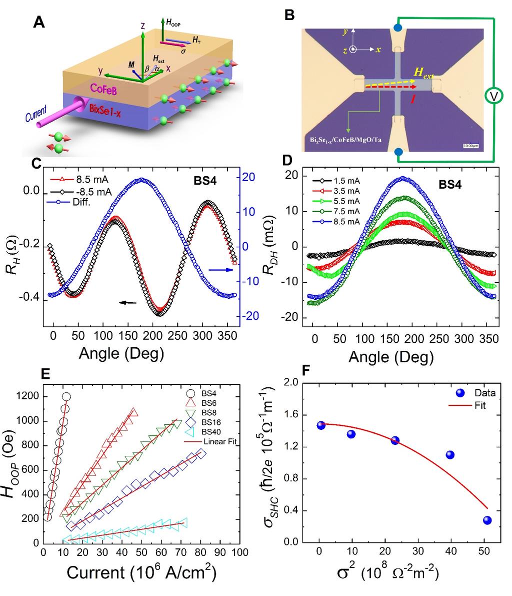
2 Currently, SOT in spin all material (SM)/ferromagnet (FM) heterostructures is of great interest due to its efficient switching of magnetization in proposed spin-based memory and logic devices (1 3). SOT has been calculated theoretically (4, 5) and observed experimentally in heavy metals (Ms)(6 10) and TIs (11 16). The in-plane charge current injected into an SM/FM/oxide heterostructure is scattered in the vertical direction, either up or down, depending upon the spin orientation of electrons due to the spin all effect (SE) (6, 7, 10, 17) or Rashba effect (9, 18). Thus, accumulated spin-polarized current in the interface between the SM and FM transfers spin angular momentum to the FM (6, 7, 19), which can rotate the magnetization of the FM and is known as SOT. Conventionally, the spin-polarized current is generated by using a ferromagnetic polarizer that transfers its spin angular momentum to a FM layer. Spin-transfer torque (STT) based devices suffer from large power consumption and reliability issues due to the low efficiency of the ferromagnetic polarizer (6, 20). SOT-based memory and logic devices are superior compared to the STT-based devices because they do not require a separate polarizer for the generation of spin-polarized current and could potentially have a much more efficient spin-current source (1, 6, 10). This results in a lower writing current density and, thus, much better device reliability. The most commonly studied spin-current generators in SM/FM heterostructures are Ms, such as Ta (6, 8, 21), W (10, 17), Pt (7, 9), and TIs such as Bi 2Se 3(11, 12, 14), and (Bi 0.5 Sb 0.5) 2Te 3 (13). It has been reported by several groups that a large current density on the order of A/cm 2 is required to switch the magnetization using SOT from Ms due to their small SA (6, 7, 9). In the case of a TI as the spin-current generator, switching of the magnetic doped TI (Cr 0.08Bi 0.54Sb 0.38) 2Te 3 layer at 1.9 K has been observed with a current density A/cm 2 (13). It is also expected that TIs will be able to demonstrate a low switching current density for the switching of magnetization at RT as a result of their large spin-orbit coupling (SOC) (11 14). owever, the switching of magnetization has not yet been observed on any TI/FM bilayer system at RT. Furthermore, the practical application of single crystalline TI grown by molecular beam epitaxy (MBE) is limited due to its strict demand on the single crystal 2
3 substrate. It is also constrained due to the presence of valleys or voids with different size and height as a result of triangular spirals (22). In this paper, we report Bi xse (1-x) films with giant spin all angles at RT grown on silicon substrate by magnetron sputtering, which is a semiconductor industry compatible process. The dc planar all method is used for the characterization of SOT in a Bi xse (1-x)/CoFeB heterostructure with in-plane magnetic easy-axis (23 25). At RT, the SA (the ratio of spin-polarized current density to charge current density) of the sputtered Bi xse (1-x) film is up to two orders of magnitude larger than that of Ms and approximately one order of magnitude greater than the crystalline TI, Bi 2Se 3. In particular, we developed a perpendicular CoFeB multilayer on Bi xse (1-x) films and demonstrated switching of the magnetization using SOT arising from the Bi xse (1-x) with the lowest switching current density in bilayers at RT. Moreover, the spin all conductivity (SC), which is the product of SA and electrical conductivity of the SM, is determined to be comparable to or larger than the previously reported values of other spincurrent generators. Furthermore, the sputtered Bi xse (1-x) layer on silicon substrate shows an excellent surface smoothness on a wafer scale for a better practical application in future. In order to characterize the SOT arising from the Bi xse (1-x) films, thin films with the multilayer structure Si/SiO 2/MgO (2 nm)/bi xse (1-x) (t BiSe nm)/cofeb (5 nm)/mgo (2 nm)/ta (5 nm) were prepared, with t BiSe= 4, 8,16, and 40 nm as shown in the schematic drawing in figure 2A. Unless otherwise stated, we will use the labeling BS4, BS8, BS16, BS40 for the samples with t BiSe= 4, 8, 16, 40 nm, respectively. Figure 1A,B shows the high-angle annular dark-field scanning transmission electron microscopy (AADF-STEM) images of samples BS4 and BS8, respectively. The AADF-STEM images show that Bi xse (1-x) has a polycrystalline structure and that the atomic layers of Bi and Se are continuous in both the BS4 and BS8 samples. Additionally, the average grain orientation in sample BS4 is 2 with a standard deviation of 9 (from vertical c-orientation), which is almost identical to the average grain orientation in the BS8 sample (2 with a standard deviation of 8 ). The energy dispersive X-ray spectroscopy (EDS) line scan shows that at the top of the Bi xse (1-x) films there is stoichiometric Bi 2Se 3; however, there is a 3
4 gradient of the Bi concentration from top to the bottom of the films (figure S2). The average ratio x in Bi xse (1-x) film is 0.47 with ± 3% uncertainty determined by the Rutherford back scattering (RBS). Figure 1C shows the atomic force microscopy (AFM) images of Si/SiO 2/MgO (2 nm)/bi xse (1-x) 4 nm film. The root mean square (RMS) value of the surface roughness of the 4 nm Bi xse (1-x) film is 0.51nm. Furthermore, we probed surface roughness propagation in full stack as shown in figure 1D. The RMS value of surface roughness 0.38 nm in BS4 sample confirms the smoothness of the full stack for future device fabrication on a wafer level. The multilayer films are patterned into all cross bars 5-30 μm wide and 70 μm long, and dc planar all measurement is performed on the all cross bar with dimensions 10 μm 70 μm, as shown in figure 2B. The bipolar input current of magnitude up to 8.5 ma is injected along the x-direction, and the angle-dependent all resistance ( R ( I, α ) ) is measured under the application of a constant 0.5 T in-plane magnetic field while rotating the sample in the xy plane from -7 to 365. The in-plane SOT exerted by the accumulated spin current on the interface of the Bi xse (1-x)/CoFeB (figure 2A) is obtained by using J s Slonczewski s equation (19), τ = ( mˆ ( ˆ σ mˆ )), where is the reduced Planck s constant, J is s 2eM t s the spin-polarized current density, e is an electronic charge, M is the saturation magnetization, t is the s thickness of the ferromagnetic layer, ˆm is the magnetization unit vector, and ˆ σ is the spin-polarized current accumulation unit vector. The associated out-of-plane magnetic field with the in-plane torque (τ ) s is given by (6) = ( ˆ σ mˆ). In addition to the in-plane torque, there is also an out-of-plane OOP ħ J 2eM t s component of SOT due to the spin accumulation at the interface, which is given by τ α ( mˆ ˆ σ) =, T where α is a coefficient that determines the efficiency of current-induced effects. The associated in- T plane magnetic field with the out-of-plane torque (τ ) is given by T = α ˆ σ. Figure 2C shows R ( I, α ) T for the sample BS4 at ± 8.5 ma. Moreover, R ( I, α ) shows two-fold symmetry with extrema at approximately 45 in increments of 90º. In principle, the R ( I, α ) consists of the planar all resistance ( 4
5 R ) and the anomalous all resistance ( PE AE R ) due to the planar and anomalous all effects, respectively. The R is due to the combined effects of the external field, current-induced effective PE fields, and the anisotropy field acting on the magnetization ( R sin( 2β ), where β is the angle between the magnetization and current flow direction). The PE R is due to the pulling of the AE magnetization in the out-of-plane direction by a current-induced effective field ( R M AE z the z-component of magnetization)., where M is z The current-induced effective fields T and OOP can be extracted by characterizing the R ( I, α ) for positive and negative input currents. The difference of the all resistance is given by (23), drae R ( I, α) = R ( I, α) R ( I, α) + 2 cosα + C (1), D PE PE OOP d where C is the resistance offset that accounts for the all bar imbalance, dr AE d is the gradient of the change in the anomalous all signal versus the externally applied out-of-plane magnetic field, and α is the angle between field and current flow direction. Figure 2D shows R ( I, α ) versus an externally applied field angle for the sample BS4 at different input currents. The R ( I, α ) increases with increase D D in input current and has a maximum located at about 180. The dr AE d is obtained by sweeping the outof-plane field at a small constant input current. After considering current shunting and short circuit effects drae (26), the d After determining the is determined to be , 7.33, -7.37, -7.55, for BS4-BS40 samples, respectively. drae d values, can be determined by curve fitting of the R OOP ( I, α D ) formula over the experimental data. The versus the current density is presented in figure 2E. The OOP OOP J SM determined by the linear fit is as large as (99.94 ± 0.17) Oe (10-6 )/ (A/cm 2 ) for the BS4 sample, where 5
6 J is the current density in the Bi SM xse (1-x) layer (the uncertainty is the standard error from the linear fit). The SA ( θ = S 2eM st OOP J SM ) of the BS4 sample is determined to be ± Sample BS4 has the largest SA value at RT that has been reported to date, which means that it is the most efficient spincurrent source at RT. The J OOP SM for BS6-BS40 samples is (23.17 ± 0.48), (14.19 ± 0.24), (9.27 ± 0.03), and (2.14 ± 0.11) Oe (10-6 )/(A/cm 2 ), respectively. The SAs for BS6-BS40 samples are determined to be 4.36 ± 0.09, 2.67 ± 0.04, 1.74 ± 0.05, 0.4 ± 0.02, respectively. The SC is defined as S 2 e θ σ, where σ is electrical conductivity of the SM. The SC is determined to be as large as 1.47 ± e Ω - 1 m -1 for the BS4 sample. The Bi xse (1-x) films have both σ and SC values comparable to previous reports on TI (11 14). A summary of σ, SA, SC for our samples and the best previously reported SMs is presented in Table 1. In our measurement technique, after we use a large in-plane magnetic field to make the CoFeB film single domain, we did not observe any significant T and Oersted field which can be clearly seen in the R ( I, α ) signal that has perfect cosα nature (figure 2D). This indicates that the large SOT in Bi xse (1- D x) films is due to the SE. The origin of SE in our Bi xse (1-x) films is investigated by studying variations of σ S with σ. Analogous to the scaling law of AE in the FM films (27, 28), the SC can be written as σ σ δσ 2 S = int, where int σ is the intrinsic SC and δ is a constant which determines the contribution of the extrinsic SE. The σ S figure 2E. By fitting the above equation over the experimental data, versus the square of electrical conductivity is presented in σ int and δ are determined to be ( ± 0.11) e Ω -1 m -1 and (-4.07 ± 0.08) Ω -1 m -1, respectively. The dominant σ int confirms 2e that the SE in the Bi xse (1-x) films is mainly due to the intrinsic SE. 6
7 The SOT arising from Bi xse (1-x) can be directly observed by switching a FM in close proximity to the spin channel(6 9). We prepared a Si/SiO 2/MgO (2 nm)/bi xse (1-x) (4 nm)/ta (0.5 nm)/cofeb (0.6 nm)/gd (1.2 nm/cofeb (1.1 nm)/mgo (2 nm)/ta (2 nm) sample and a control sample Si/SiO 2/MgO (2 nm)/ta (5 nm)/cofeb (0.6 nm)/gd (1.2 nm)/cofeb (1.1 nm)/mgo (2 nm)/ta (2 nm) for the switching experiment. The films were patterned into all cross bars using optical lithography. Figure 3B shows the R loop of the Bi AE xse (1-x) switching sample obtained by sweeping the out-of-plane field at a constant input current of 50 μa. The non-zero R at zero magnetic field confirms the easy axis of the AE magnetization along the out-of-plane direction. The perpendicular magnetic anisotropy (PMA) originated from the exchange interaction between the CoFeB and Gd layers. The R loops of the Bi AE xse (1-x) switching sample as a result of dc current sweep under the application of a constant in-plane bias field along the current channel are shown in figure 3C,D. In the presence of a + 80 Oe bias field (figure 3C), the dc current sweep from positive to negative favors the magnetization in the downward direction (M z<0), and the magnetization switching occurs at -7 ma (~ A/cm 2 ). The subsequent reverse sweep from negative to positive current at identical magnitude and direction of the field favors the magnetization in the upward direction (M z>0), and the magnetization switching occurs at 7 ma. Upon changing the polarity of the external field, the chirality of the R loop changes, which is consistent with AE the results of previous reports (6 8). The steps in switching confirm that the switching is mainly due to the domain wall nucleation and domain wall motion. The orientation of the R loop in the Ta switching AE sample is opposite to the Bi xse (1-x) switching sample, which suggests that the two samples do have opposite SA polarity (figures 3C,D, and S5C,S5D). We also calculate the switching efficiency (29), η k x =, where k J sw is the anisotropy field, is the external bias field, and J is the switching x sw current density. The switching efficiency of the Bi xse (1-x) is determined to be 2.57 koe per 10 5 A/cm 2. The Ta has switching efficiency of 4.7 koe per 10 7 A/cm 2, which is comparable to the previous reports (29). The two orders of magnitude larger switching efficiency and opposite R loop orientation in the Bi AE xse (1-7
8 x) switching sample compared to those of the Ta switching sample confirm that the switching is due to SOT from the 4 nm thick Bi xse (1-x) layer rather than the 0.5 nm thick Ta insertion layer in the Bi xse (1-x) switching sample. One of the key factors for widespread realization of SOT-based spintronic devices is the development of a spin all channel with a high spin current generation efficiency. This leads to a low switching current density of the adjacent magnet and paves the way for ease of integration of spintronic devices with semiconductors. Moreover, the development of a smooth SM interface at low thermal budget must be achievable. We demonstrated the growth of smooth Bi xse (1-x) films on a large silicon wafer with the largest SA ever reported using a semiconductor industry compatible sputtering process. These films possess comparable or better SC compared to other reported spin-current generators at RT. Furthermore, we developed and switched a perpendicular CoFeB multilayer on Bi xse (1-x) films for the first time at RT by a TI material, which enables a path for reliable and efficient beyond-cmos devices. It should be pointed out that the Bi xse (1-x) in this study is still not optimized, so there is a wide window to improve the characteristics of Bi xse (1-x) as a spin all channel. ACKNOWLEDGMENTS We would like to thank Prof. Paul Crowell for proofreading the manuscript and Prof. M. Kawaguchi for helpful discussions on data analysis. Funding: This work was supported by C-SPIN, one of six STARnet program research centers. This work utilized (1) the College of Science and Engineering (CSE) Characterization Facility, University of Minnesota (UM), supported in part by the NSF through the UMN MRSEC program (No. DMR ); and (2) the CSE Minnesota Nano Center, UM, supported in part by NSF through the NNIN program. 8
9 References and Notes 1. A. Brataas et al., Nat. Nanotechnol. 9, (2014). 2. S. Manipatruni et al., Appl. Phys. Express. 7 (2014), doi: /apex M. Cubukcu et al., Appl. Phys. Lett. 104 (2014), doi: / A. Manchon et al., Phys. Rev. B. 79, (2009). 5. X. Wang et al., Phys. Rev. B - Condens. Matter Mater. Phys. 89, 1 11 (2014). 6. L. Liu et al., Science (80-. ). 336, (2012). 7. L. Liu et al., Phys. Rev. Lett. 109, 1 5 (2012). 8. Z. Zhao et al., Appl. Phys. Lett. 106, 0 4 (2015). 9. I. M. Miron et al., Nature. 476, (2011). 10. C. F. Pai et al., Appl. Phys. Lett. 101, 1 5 (2012). 11. M. Jamali et al., Nano Lett. 15, (2015). 12. A. R. Mellnik et al., Nature. 511, (2014). 13. Y. Fan et al., Nat. Mater. 13, (2014). 14. Y. Wang et al., Phys. Rev. Lett. 114, 1 5 (2015). 15. Y. Shiomi et al., Phys. Rev. Lett. 113, 7 11 (2014). 16. C.. Li et al.,nat. Commun., 1 8 (2016). 17. Q. ao et al.,phys. Rev. Appl. 3, (2015). 18. T. Suzuki et al., Appl. Phys. Lett. 98, 1 4 (2011). 19. J. C. Slonczewski, J. Magn. Magn. Mater (1996). 20. C. Chappert et al., Nat. Mater. 6, (2007). 21. J. Kim et al., Nat. Mater. 12, (2013). 22. S. Schreyeck et al., Appl. Phys. Lett. 102 (2013), doi: / M. Kawaguchi et al., Appl. Phys. Express. 6 (2013), doi: /apex M. Jamali et al., J. Appl. Phys. 119, 0 5 (2016). 25. K. Garello et al., Nat. Nanotechnol. 8, (2013). 26. W. J. Xu et al., Eur. Phys. J. B. 65, (2008). 27. Y. Tian et al., Phys. Rev. Lett. 103 (2009), doi: /physrevlett E. Sagasta et al., Phys. Rev. B - Condens. Matter Mater. Phys. 94, 1 6 (2016). 29. J. Yu et al., Appl. Phys. Lett. 109 (2016), doi: /
 atomic detail.")
10 Fig. 1. STEM and surface roughness characterization. (A) and (B) Composites of simultaneously acquired BF- and AADF-STEM images of samples BS4 and BS8, respectively. The selected region of the AADF-STEM image indicated by a black line is magnified at right to show the Bi xse (1-x) atomic detail. The AFM images of (C) 4 nm Bi x Se (1-x) film and (D) BS4 sample. 10
11 Fig. 2. Schematic diagram, experimental set up, angle-dependent all resistance measurements, and characterization of SOT. (A) A three-dimensional schematic diagram demonstrating the SOT in a Bi xse (1-x)/CoFeB heterostructure. ext and M represent an in-plane externally applied magnetic field and the in-plane magnetization, respectively. T and OOP are the current-induced transverse and out-of-plane magnetic fields, respectively. (B) An optical micrograph of the fabricated all cross bar with schematic drawings of the all measurement set up. (C) The R ( I, α ) of sample BS4 at ± 8.5 ma input current on the left axis and R ( I, α ) on the right axis at RT under a constant 0.5 T in-plane magnetic field. (D) The RD D ( I, α ) at different input currents for the BS4 sample. (E) The OOP variation with the current density. (F) The σ SC change with respect to the linear conductivity squared. 11
12 12
13 Fig. 3. Current-induced magnetization switching in the Bi xse (1-x) (4 nm)/ta (0.5 nm)/cofeb(0.6 nm)/gd (1.2 nm)/cofeb (1.1 nm) heterostructure. (A) A schematic drawing of the switching sample stack structure. (B) The R measured in the Bi AE xse (1-x) switching sample using a 50 μa current. (C) and (D) Current-induced switching of the magnetization due to the SOT arising from the Bi xse (1-x) underlayer in the presence of a constant 8 mt in-plane bias field measured in all cross bar with dimensions 15 μm 70 μm. 13
14 Table 1. A summary of the θ, σ S S, J, and σ of the SMs in this work and best previous reports. sw Parameters Bi xse (1-x) (This work) (RT) (Bi 0.5 Sb 0.5) 2Te 3 (Ref. 13) (1.9 K) Bi 2Se 3 (Ref. 12 ) (RT) β -Ta (Ref. 6) (RT) β -W (Ref. 17) (RT) Pt (Ref. 7, 9) (RT) σ (Ω -1 m -1 ) ħ σ S (10 5 Ω -1 m -1 ) 2e θ S sw J (A/cm 2 )
MSE 7025 Magnetic Materials (and Spintronics)
") MSE 7025 Magnetic Materials (and Spintronics) Lecture 14: Spin Transfer Torque And the future of spintronics research Chi-Feng Pai cfpai@ntu.edu.tw Course Outline Time Table Week Date Lecture 1 Feb 24
MSE 7025 Magnetic Materials (and Spintronics) Lecture 14: Spin Transfer Torque And the future of spintronics research Chi-Feng Pai cfpai@ntu.edu.tw Course Outline Time Table Week Date Lecture 1 Feb 24
Room temperature spin-orbit torque switching induced by a
 Room temperature spin-orbit torque switching induced by a topological insulator Jiahao Han 1, A. Richardella 2, Saima Siddiqui 1, Joseph Finley 1, N. Samarth 2 and Luqiao Liu 1* 1 Department of Electrical
0.002 ( ) R xy
 R xy") a b z 0.002 x H y R xy () 0.000-0.002 0 90 180 270 360 (degree) Supplementary Figure 1. Planar Hall effect resistance as a function of the angle of an in-plane field. a, Schematic of the planar Hall resistance
a b z 0.002 x H y R xy () 0.000-0.002 0 90 180 270 360 (degree) Supplementary Figure 1. Planar Hall effect resistance as a function of the angle of an in-plane field. a, Schematic of the planar Hall resistance
SUPPLEMENTARY INFORMATION
 Magnetization switching through giant spin-orbit torque in a magnetically doped topological insulator heterostructure Yabin Fan, 1,,* Pramey Upadhyaya, 1, Xufeng Kou, 1, Murong Lang, 1 So Takei, 2 Zhenxing
Spin orbit torque driven magnetic switching and memory. Debanjan Bhowmik
 Spin orbit torque driven magnetic switching and memory Debanjan Bhowmik Spin Transfer Torque Fixed Layer Free Layer Fixed Layer Free Layer Current coming out of the fixed layer (F2) is spin polarized in
Enhanced spin orbit torques by oxygen incorporation in tungsten films
 Enhanced spin orbit torques by oxygen incorporation in tungsten films Timothy Phung IBM Almaden Research Center, San Jose, California, USA 1 Motivation: Memory devices based on spin currents Spin Transfer
SUPPLEMENTARY INFORMATION
 SUPPLEMENTARY INFORMATION DOI: 10.1038/NNANO.2014.16 Electrical detection of charge current-induced spin polarization due to spin-momentum locking in Bi 2 Se 3 by C.H. Li, O.M.J. van t Erve, J.T. Robinson,
Emerging spintronics-based logic technologies
 Center for Spintronic Materials, Interfaces, and Novel Architectures Emerging spintronics-based logic technologies Zhaoxin Liang Meghna Mankalale Jian-Ping Wang Sachin S. Sapatnekar University of Minnesota
External-Field-Free Spin Hall Switching of Perpendicular Magnetic Nanopillar with a Dipole-Coupled Composite Structure
 External-Field-Free Spin Hall Switching of Perpendicular Magnetic Nanopillar with a Dipole-Coupled Composite Structure Zhengyang Zhao, Angeline K. Smith, Mahdi Jamali, and Jian-Ping Wang * Department of
Spin dynamics in Bi 2 Se 3 /ferromagnet heterostructures
 Spin dynamics in Bi 2 Se 3 /ferromagnet heterostructures Hyunsoo Yang Electrical and Computer Engineering, National University of Singapore eleyang@nus.edu.sg Outline Spin-orbit torque (SOT) engineering
Hidden Interfaces and High-Temperature Magnetism in Intrinsic Topological Insulator - Ferromagnetic Insulator Heterostructures
 Hidden Interfaces and High-Temperature Magnetism in Intrinsic Topological Insulator - Ferromagnetic Insulator Heterostructures Valeria Lauter Quantum Condensed Matter Division, Oak Ridge National Laboratory,
Spin pumping in Ferromagnet-Topological Insulator-Ferromagnet Heterostructures Supplementary Information.
 Spin pumping in Ferromagnet-Topological Insulator-Ferromagnet Heterostructures Supplementary Information. A.A. Baker,, 2 A.I. Figueroa, 2 L.J. Collins-McIntyre, G. van der Laan, 2 and T., a) Hesjedal )
Planar Hall Effect in Magnetite (100) Films
 Films") Planar Hall Effect in Magnetite (100) Films Xuesong Jin, Rafael Ramos*, Y. Zhou, C. McEvoy and I.V. Shvets SFI Nanoscience Laboratories, School of Physics, Trinity College Dublin, Dublin 2, Ireland 1 Abstract.
Planar Hall Effect in Magnetite (100) Films Xuesong Jin, Rafael Ramos*, Y. Zhou, C. McEvoy and I.V. Shvets SFI Nanoscience Laboratories, School of Physics, Trinity College Dublin, Dublin 2, Ireland 1 Abstract.
Two-terminal spin orbit torque magnetoresistive random access memory
 Two-terminal spin orbit torque magnetoresistive random access memory Noriyuki Sato 1, Fen Xue 1,3, Robert M. White 1,2, Chong Bi 1, and Shan X. Wang 1,2,* 1 Stanford University, Department of Electrical
Spin-orbit torque in Pt/CoNiCo/Pt symmetric devices
 Spin-orbit torque in Pt/CoNiCo/Pt symmetric devices Meiyin Yang 1, Kaiming Cai 1, Hailang Ju 2, Kevin William Edmonds 3, Guang Yang 4, Shuai Liu 2, Baohe Li 2, Bao Zhang 1, Yu Sheng 1, ShouguoWang 4, Yang
Optical studies of current-induced magnetization
 Optical studies of current-induced magnetization Virginia (Gina) Lorenz Department of Physics, University of Illinois at Urbana-Champaign PHYS403, December 5, 2017 The scaling of electronics John Bardeen,
Anisotropic Current-Controlled Magnetization Reversal in the Ferromagnetic Semiconductor (Ga,Mn)As
As") Anisotropic Current-Controlled Magnetization Reversal in the Ferromagnetic Semiconductor (Ga,Mn)As Yuanyuan Li 1, Y. F. Cao 1, G. N. Wei 1, Yanyong Li 1, Y. i and K. Y. Wang 1,* 1 SKLSM, Institute of Semiconductors,
Anisotropic Current-Controlled Magnetization Reversal in the Ferromagnetic Semiconductor (Ga,Mn)As Yuanyuan Li 1, Y. F. Cao 1, G. N. Wei 1, Yanyong Li 1, Y. i and K. Y. Wang 1,* 1 SKLSM, Institute of Semiconductors,
Current-driven Magnetization Reversal in a Ferromagnetic Semiconductor. (Ga,Mn)As/GaAs/(Ga,Mn)As Tunnel Junction
As/GaAs/(Ga,Mn)As Tunnel Junction") Current-driven Magnetization Reversal in a Ferromagnetic Semiconductor (Ga,Mn)As/GaAs/(Ga,Mn)As Tunnel Junction D. Chiba 1, 2*, Y. Sato 1, T. Kita 2, 1, F. Matsukura 1, 2, and H. Ohno 1, 2 1 Laboratory
Current-driven Magnetization Reversal in a Ferromagnetic Semiconductor (Ga,Mn)As/GaAs/(Ga,Mn)As Tunnel Junction D. Chiba 1, 2*, Y. Sato 1, T. Kita 2, 1, F. Matsukura 1, 2, and H. Ohno 1, 2 1 Laboratory
S. Mangin 1, Y. Henry 2, D. Ravelosona 3, J.A. Katine 4, and S. Moyerman 5, I. Tudosa 5, E. E. Fullerton 5
 Spin transfer torques in high anisotropy magnetic nanostructures S. Mangin 1, Y. enry 2, D. Ravelosona 3, J.A. Katine 4, and S. Moyerman 5, I. Tudosa 5, E. E. Fullerton 5 1) Laboratoire de Physique des
Spin Hall effect clocking of nanomagnetic logic without a magnetic field
 SUPPLEMENTARY INFORMATION DOI: 10.1038/NNANO.2013.241 Spin Hall effect clocking of nanomagnetic logic without a magnetic field (Debanjan Bhowmik *, Long You *, Sayeef Salahuddin) Supplementary Section
SUPPLEMENTARY INFORMATION
 SUPPLEMENTARY INFORMATION Reversible Electric Control of Exchange Bias in a Multiferroic Field Effect Device S. M. Wu 1, 2, Shane A. Cybart 1, 2, P. Yu 1, 2, M. D. Abrodos 1, J. Zhang 1, R. Ramesh 1, 2
Current-induced switching in a magnetic insulator
 In the format provided by the authors and unedited. DOI: 10.1038/NMAT4812 Current-induced switching in a magnetic insulator Can Onur Avci, Andy Quindeau, Chi-Feng Pai 1, Maxwell Mann, Lucas Caretta, Astera
Angular and temperature dependence of current induced spin-orbit effective fields in Ta/CoFeB/MgO nanowires
 Supplementary Information Angular and temperature dependence of current induced spin-orbit effective fields in Ta/CoFeB/MgO nanowires Xuepeng Qiu 1, Praveen Deorani 1, Kulothungasagaran Narayanapillai
Spin orbit torques and Dzyaloshinskii-Moriya interaction in dualinterfaced
 Supplementary Information Spin orbit torques and Dzyaloshinskii-Moriya interaction in dualinterfaced Co-Ni multilayers Jiawei Yu, Xuepeng Qiu, Yang Wu, Jungbum Yoon, Praveen Deorani, Jean Mourad Besbas,
Physics in Quasi-2D Materials for Spintronics Applications
 Physics in Quasi-2D Materials for Spintronics Applications Topological Insulators and Graphene Ching-Tzu Chen IBM TJ Watson Research Center May 13, 2016 2016 C-SPIN Topological Spintronics Device Workshop
Cover Page. The handle holds various files of this Leiden University dissertation
 Cover Page The handle http://hdl.handle.net/1887/24306 holds various files of this Leiden University dissertation Author: Verhagen, T.G.A. Title: Magnetism and magnetization dynamics in thin film ferromagnets
An Overview of Spintronics in 2D Materials
 An Overview of Spintronics in 2D Materials Wei Han ( 韩伟 ) 1 2014 ICQM Outline I. Introduction to spintronics (Lecture I) II. Spin injection and detection in 2D (Lecture I) III. Putting magnetic moment
Perpendicular MTJ stack development for STT MRAM on Endura PVD platform
 Perpendicular MTJ stack development for STT MRAM on Endura PVD platform Mahendra Pakala, Silicon Systems Group, AMAT Dec 16 th, 2014 AVS 2014 *All data in presentation is internal Applied generated data
TRANSVERSE SPIN TRANSPORT IN GRAPHENE
 International Journal of Modern Physics B Vol. 23, Nos. 12 & 13 (2009) 2641 2646 World Scientific Publishing Company TRANSVERSE SPIN TRANSPORT IN GRAPHENE TARIQ M. G. MOHIUDDIN, A. A. ZHUKOV, D. C. ELIAS,
FIG. 1: (Supplementary Figure 1: Large-field Hall data) (a) AHE (blue) and longitudinal
 (a) AHE (blue) and longitudinal") FIG. 1: (Supplementary Figure 1: Large-field Hall data) (a) AHE (blue) and longitudinal MR (red) of device A at T =2 K and V G - V G 0 = 100 V. Bold blue line is linear fit to large field Hall data (larger
FIG. 1: (Supplementary Figure 1: Large-field Hall data) (a) AHE (blue) and longitudinal MR (red) of device A at T =2 K and V G - V G 0 = 100 V. Bold blue line is linear fit to large field Hall data (larger
Mesoscopic Spintronics
 Mesoscopic Spintronics Taro WAKAMURA (Université Paris-Sud) Lecture 1 Today s Topics 1.1 History of Spintronics 1.2 Fudamentals in Spintronics Spin-dependent transport GMR and TMR effect Spin injection
Magnetoresistance due to Domain Walls in Micron Scale Fe Wires. with Stripe Domains arxiv:cond-mat/ v1 [cond-mat.mes-hall] 9 Mar 1998.
![Magnetoresistance due to Domain Walls in Micron Scale Fe Wires. with Stripe Domains arxiv:cond-mat/ v1 [cond-mat.mes-hall] 9 Mar 1998.](/thumbs/90/104152266.jpg "Magnetoresistance due to Domain Walls in Micron Scale Fe Wires. with Stripe Domains arxiv:cond-mat/ v1 [cond-mat.mes-hall] 9 Mar 1998.") Magnetoresistance due to Domain Walls in Micron Scale Fe Wires with Stripe Domains arxiv:cond-mat/9803101v1 [cond-mat.mes-hall] 9 Mar 1998 A. D. Kent a, U. Ruediger a, J. Yu a, S. Zhang a, P. M. Levy a
Magnetoresistance due to Domain Walls in Micron Scale Fe Wires with Stripe Domains arxiv:cond-mat/9803101v1 [cond-mat.mes-hall] 9 Mar 1998 A. D. Kent a, U. Ruediger a, J. Yu a, S. Zhang a, P. M. Levy a
Room Temperature Planar Hall Transistor
 Room Temperature Planar Hall Transistor Bao Zhang 1, Kangkang Meng 1, Mei-Yin Yang 1, K. W. Edmonds 2, Hao Zhang 1, Kai-Ming Cai 1, Yu Sheng 1,3, Nan Zhang 1, Yang Ji 1, Jian-Hua Zhao 1, Kai-You Wang 1*
Ferromagnetic Domain Distribution in Thin Films During Magnetization Reversal. and E. D. Dahlberg 3. Abstract
 Ferromagnetic Domain Distribution in Thin Films During Magnetization Reversal W.-T. Lee 1, S. G. E. te Velthuis 2, G. P. Felcher 2, F. Klose 1, T. Gredig 3, and E. D. Dahlberg 3. 1 Spallation Neutron Source,
Imprinting domain/spin configurations in antiferromagnets. A way to tailor hysteresis loops in ferromagnetic-antiferromagnetic systems
 Imprinting domain/spin configurations in antiferromagnets A way to tailor hysteresis loops in ferromagnetic-antiferromagnetic systems Dr. J. Sort Institució Catalana de Recerca i Estudis Avançats (ICREA)
Determination of the Interfacial Dzyaloshinskii-Moriya Interaction (idmi) in the Inversion Symmetry Broken Systems
 in the Inversion Symmetry Broken Systems") Determination of the Interfacial Dzyaloshinskii-Moriya Interaction (idmi) in the Inversion Symmetry Broken Systems 27 Nov. 2015 Chun-Yeol You (cyyou@inha.ac.kr) Dept. of Physics, Inha University, Korea
Determination of the Interfacial Dzyaloshinskii-Moriya Interaction (idmi) in the Inversion Symmetry Broken Systems 27 Nov. 2015 Chun-Yeol You (cyyou@inha.ac.kr) Dept. of Physics, Inha University, Korea
Quantitative characterization of spin-orbit torques in Pt/Co/Pt /Co/Ta/BTO heterostructure on the magnetization azimuthal angle dependence
 Quantitative characterization of spin-orbit torques in Pt/Co/Pt /Co/Ta/BTO heterostructure on the magnetization azimuthal angle dependence Christian Engel, Sarjoosing Goolaup, Feilong Luo, and Wen Siang
Mesoscopic Spintronics
 Mesoscopic Spintronics Taro WAKAMURA (Université Paris-Sud) Lecture 2 Today s Topics 2.1 Anomalous Hall effect and spin Hall effect 2.2 Spin Hall effect measurements 2.3 Interface effects Anomalous Hall
Electric-field control of spin-orbit torque in a magnetically doped topological. insulator
 Electric-field control of spin-orbit torque in a magnetically doped topological insulator Yabin Fan 1 *, Xufeng Kou 1, Pramey Upadhyaya 1, Qiming Shao 1, Lei Pan 1, Murong Lang 1, Xiaoyu Che 1, Jianshi
Focused-ion-beam milling based nanostencil mask fabrication for spin transfer torque studies. Güntherodt
 Focused-ion-beam milling based nanostencil mask fabrication for spin transfer torque studies B. Özyilmaz a, G. Richter, N. Müsgens, M. Fraune, M. Hawraneck, B. Beschoten b, and G. Güntherodt Physikalisches
Anisotropy Distributions in Patterned Magnetic Media
 MINT Review & Workshop 24-25 Oct. 2006 Anisotropy Distributions in Patterned Magnetic Media Tom Thomson Hitachi San Jose Research Center Page 1 Acknowledgements Manfred Albrecht (Post-doc) Tom Albrecht
SUPPLEMENTARY INFORMATION
 In the format provided by the authors and unedited. DOI:.38/NMAT4855 A magnetic heterostructure of topological insulators as a candidate for axion insulator M. Mogi, M. Kawamura, R. Yoshimi, A. Tsukazaki,
voltage measurement for spin-orbit torques"
 SUPPLEMENTARY for article "Accurate analysis for harmonic Hall voltage measurement for spin-orbit torques" Seok Jin Yun, 1 Eun-Sang Park, 2 Kyung-Jin Lee, 1,2 and Sang Ho Lim 1,* 1 Department of Materials
Putting the Electron s Spin to Work Dan Ralph Kavli Institute at Cornell Cornell University
 Putting the Electron s Spin to Work Dan Ralph Kavli Institute at Cornell Cornell University Yongtao Cui, Ted Gudmundsen, Colin Heikes, Wan Li, Alex Mellnik, Takahiro Moriyama, Joshua Parks, Sufei Shi,
SPIN TRANSFER TORQUES IN HIGH ANISOTROPY MAGNETIC NANOSTRUCTURES
 CRR Report Number 29, Winter 2008 SPIN TRANSFER TORQUES IN HIGH ANISOTROPY AGNETIC NANOSTRUCTURES Eric Fullerton 1, Jordan Katine 2, Stephane angin 3, Yves Henry 4, Dafine Ravelosona 5, 1 University of
Solid Surfaces, Interfaces and Thin Films
 Hans Lüth Solid Surfaces, Interfaces and Thin Films Fifth Edition With 427 Figures.2e Springer Contents 1 Surface and Interface Physics: Its Definition and Importance... 1 Panel I: Ultrahigh Vacuum (UHV)
All-electrical measurements of direct spin Hall effect in GaAs with Esaki diode electrodes.
 All-electrical measurements of direct spin Hall effect in GaAs with Esaki diode electrodes. M. Ehlert 1, C. Song 1,2, M. Ciorga 1,*, M. Utz 1, D. Schuh 1, D. Bougeard 1, and D. Weiss 1 1 Institute of Experimental
arxiv: v1 [cond-mat.mtrl-sci] 28 Jul 2008
![arxiv: v1 [cond-mat.mtrl-sci] 28 Jul 2008](/thumbs/88/117898456.jpg "arxiv: v1 [cond-mat.mtrl-sci] 28 Jul 2008") Current induced resistance change of magnetic tunnel junctions with ultra-thin MgO tunnel barriers Patryk Krzysteczko, 1, Xinli Kou, 2 Karsten Rott, 1 Andy Thomas, 1 and Günter Reiss 1 1 Bielefeld University,
Current induced resistance change of magnetic tunnel junctions with ultra-thin MgO tunnel barriers Patryk Krzysteczko, 1, Xinli Kou, 2 Karsten Rott, 1 Andy Thomas, 1 and Günter Reiss 1 1 Bielefeld University,
Nano and micro Hall-effect sensors for room-temperature scanning hall probe microscopy
 Microelectronic Engineering 73 74 (2004) 524 528 www.elsevier.com/locate/mee Nano and micro Hall-effect sensors for room-temperature scanning hall probe microscopy A. Sandhu a, *, A. Okamoto b, I. Shibasaki
Supplementary Figure 1. Magneto-transport characteristics of topological semimetal Cd 3 As 2 microribbon. (a) Measured resistance (R) as a function
 Measured resistance (R) as a function") Supplementary Figure 1. Magneto-transport characteristics of topological semimetal Cd 3 As 2 microribbon. (a) Measured resistance (R) as a function of temperature (T) at zero magnetic field. (b) Magnetoresistance
Supplementary Figure 1. Magneto-transport characteristics of topological semimetal Cd 3 As 2 microribbon. (a) Measured resistance (R) as a function of temperature (T) at zero magnetic field. (b) Magnetoresistance
Graphene photodetectors with ultra-broadband and high responsivity at room temperature
 SUPPLEMENTARY INFORMATION DOI: 10.1038/NNANO.2014.31 Graphene photodetectors with ultra-broadband and high responsivity at room temperature Chang-Hua Liu 1, You-Chia Chang 2, Ted Norris 1.2* and Zhaohui
Stripes developed at the strong limit of nematicity in FeSe film
 Stripes developed at the strong limit of nematicity in FeSe film Wei Li ( ) Department of Physics, Tsinghua University IASTU Seminar, Sep. 19, 2017 Acknowledgements Tsinghua University Prof. Qi-Kun Xue,
Spin-torque nano-oscillators trends and challenging
 Domain Microstructure and Dynamics in Magnetic Elements Heraklion, Crete, April 8 11, 2013 Spin-torque nano-oscillators trends and challenging N H ext S Giovanni Finocchio Department of Electronic Engineering,
Fermi level dependent charge-to-spin current conversion by Dirac surface state of topological insulators
 Fermi level dependent charge-to-spin current conversion by Dirac surface state of topological insulators K. Kondou 1*, R. Yoshimi 2, A. Tsukazaki 3, Y. Fukuma 1,4, J. Matsuno 1, K. S. Takahashi 1, M. Kawasaki
Angular dependence of the magnetization reversal in exchange biased Fe/MnF 2. Elke Arenholz
 Angular dependence of the magnetization reversal in exchange biased Fe/MnF 2 Elke Arenholz Advanced Light Source, Lawrence Berkeley National Laboratory, Berkeley, CA 94720 Kai Liu Department of Physics,
ANGULAR DEPENDENCE OF MAGNETIC PROPERTIES IN Co/Pt MULTILAYERS WITH PERPENDICULAR MAGNETIC ANISOTROPY
 International Journal of Modern Physics B Vol. 19, Nos. 15, 16 & 17 (2005) 2562-2567 World Scientific Publishing Company World Scientific V www.worldscientific.com ANGULAR DEPENDENCE OF MAGNETIC PROPERTIES
Magnetic oscillations driven by the spin Hall effect in 3-terminal magnetic tunnel junction. devices. Cornell University, Ithaca, NY 14853
 Magnetic oscillations driven by the spin Hall ect in 3-terminal magnetic tunnel junction devices Luqiao Liu 1, Chi-Feng Pai 1, D. C. Ralph 1,2, R. A. Buhrman 1 1 Cornell University, Ithaca, NY 14853 2
Supplementary Information for Atomically Phase-Matched Second-Harmonic Generation. in a 2D Crystal
 Supplementary Information for Atomically Phase-Matched Second-Harmonic Generation in a 2D Crystal Mervin Zhao 1, 2, Ziliang Ye 1, 2, Ryuji Suzuki 3, 4, Yu Ye 1, 2, Hanyu Zhu 1, Jun Xiao 1, Yuan Wang 1,
Spin Funneling for Enhanced Spin Injection into Ferromagnets: Supplementary Information
 Spin Funneling for Enhanced Spin Injection into Ferromagnets: Supplementary Information Shehrin Sayed, Vinh Q. Diep, Kerem Yunus Camsari, and Supriyo Datta School of Electrical and Computer Engineering,
Title of file for HTML: Supplementary Information Description: Supplementary Figures and Supplementary References
 Title of file for HTML: Supplementary Information Description: Supplementary Figures and Supplementary References Supplementary Figure 1. SEM images of perovskite single-crystal patterned thin film with
Magneto-Seebeck effect in spin-valve with in-plane thermal gradient
 Magneto-Seebeck effect in spin-valve with in-plane thermal gradient S. Jain 1, a), D. D. Lam 2, b), A. Bose 1, c), H. Sharma 3, d), V. R. Palkar 1, e), C. V. Tomy 3, f), Y. Suzuki 2, g) 1, h) and A. A.
X-Ray Spectro-Microscopy Joachim Stöhr Stanford Synchrotron Radiation Laboratory
 X-Ray Spectro-Microscopy Joachim Stöhr Stanford Synchrotron Radiation Laboratory X-Rays have come a long way Application to Magnetic Systems 1 µm 1895 1993 2003 http://www-ssrl.slac.stanford.edu/stohr/index.htm
Spatiotemporal magnetic imaging at the nanometer and picosecond scales
 AFOSR Nanoelectronics Review, Oct. 24, 2016 Spatiotemporal magnetic imaging at the nanometer and picosecond scales Gregory D. Fuchs School of Applied & Engineering Physics, Cornell University T M V TRANE
Material Science II. d Electron systems
 Material Science II. d Electron systems 1. Electronic structure of transition-metal ions (May 23) 2. Crystal structure and band structure (June 13) 3. Mott s (June 20) 4. Metal- transition (June 27) 5.
Magnon-drag thermopile
 Magnon-drag thermopile I. DEVICE FABRICATION AND CHARACTERIZATION Our devices consist of a large number of pairs of permalloy (NiFe) wires (30 nm wide, 20 nm thick and 5 µm long) connected in a zigzag
Planar Hall Effect Based Characterization of Spin Orbital Torques in Ta/CoFeB/MgO Structures
 Planar Hall Effect Based Characterization of Spin Orbital Torques in Ta/CoFeB/MgO Structures Mahdi Jamali 1, Zhengyang Zhao 1, Mahendra DC 2, Delin Zhang 1, Hongshi Li 3, Angeline K. Smith 1, Jian-Ping
Current-induced four-state magnetization switching by spin-orbit torques in. perpendicular ferromagnetic trilayers
 Current-induced four-state magnetization switching by spin-orbit torques in perpendicular ferromagnetic trilayers Y. Sheng, 1,2 Y. C. Li, 2,3 X. Q. Ma, 1 K. Y. Wang 2,3,4 1 Department of Physics, University
Anomalous Hall Effect in Fe/Gd Bilayers
 Anomalous Hall Effect in Fe/Gd Bilayers W. J. Xu 1, B. Zhang 2, Z. X. Liu 1, Z. Wang 1, W. Li 1, Z. B. Wu 3, R. H. Yu 4 and X. X. Zhang 2* 1 Dept. of Phys. and Institute of Nanoscience & Technology, The
Influence of Size on the Properties of Materials
 Influence of Size on the Properties of Materials M. J. O Shea Kansas State University mjoshea@phys.ksu.edu If you cannot get the papers connected to this work, please e-mail me for a copy 1. General Introduction
From Spin Torque Random Access Memory to Spintronic Memristor. Xiaobin Wang Seagate Technology
 From Spin Torque Random Access Memory to Spintronic Memristor Xiaobin Wang Seagate Technology Contents Spin Torque Random Access Memory: dynamics characterization, device scale down challenges and opportunities
Effect of heavy metal layer thickness on spin-orbit torque and current-induced. switching in Hf CoFeB MgO structures 90095, USA USA.
 Effect of heavy metal layer thickness on spin-orbit torque and current-induced switching in Hf CoFeB MgO structures Mustafa Akyol, 1, 2 Wanjun Jiang, 3 Guoqiang Yu, 1 Yabin Fan, 1 Mustafa Gunes, 4 Ahmet
Supplementary figures
 Supplementary figures Supplementary Figure 1. A, Schematic of a Au/SRO113/SRO214 junction. A 15-nm thick SRO113 layer was etched along with 30-nm thick SRO214 substrate layer. To isolate the top Au electrodes
Electric field control of magnetization using AFM/FM interfaces. Xiaoshan Xu
 Electric field control of magnetization using AFM/FM interfaces Xiaoshan Xu Magnetoelectric effects α = μ 0 M E H M H = 0, E = 0 = 0 (General magnetoelectrics) M H = 0, E = 0 0, P H = 0, E = 0 0, (Multiferroics)
Switching of perpendicular magnetization by spin-orbit torques in the absence of. external magnetic fields. California 90095, United States
 Switching of perpendicular magnetization by spin-orbit torques in the absence of external magnetic fields Guoqiang Yu 1 *, Pramey Upadhyaya 1, Yabin Fan 1, Juan G Alzate 1, Wanjun Jiang 1, Kin L. Wong
Lecture I. Spin Orbitronics
 Lecture I Spin Orbitronics Alireza Qaiumzadeh Radboud University (RU) Institute for Molecules and Materials (IMM) Theory of Condensed Matter group (TCM) What We Talk About When We Talk About Spin Orbitronics
Observation of topological surface state quantum Hall effect in an intrinsic three-dimensional topological insulator
 Observation of topological surface state quantum Hall effect in an intrinsic three-dimensional topological insulator Authors: Yang Xu 1,2, Ireneusz Miotkowski 1, Chang Liu 3,4, Jifa Tian 1,2, Hyoungdo
SUPPLEMENTARY INFORMATION
 Lateral heterojunctions within monolayer MoSe 2 -WSe 2 semiconductors Chunming Huang 1,#,*, Sanfeng Wu 1,#,*, Ana M. Sanchez 2,#,*, Jonathan J. P. Peters 2, Richard Beanland 2, Jason S. Ross 3, Pasqual
SUPPLEMENTARY INFORMATION
 Dirac electron states formed at the heterointerface between a topological insulator and a conventional semiconductor 1. Surface morphology of InP substrate and the device Figure S1(a) shows a 10-μm-square
Intrinsic Electronic Transport Properties of High. Information
 Intrinsic Electronic Transport Properties of High Quality and MoS 2 : Supporting Information Britton W. H. Baugher, Hugh O. H. Churchill, Yafang Yang, and Pablo Jarillo-Herrero Department of Physics, Massachusetts
Current-driven ferromagnetic resonance, mechanical torques and rotary motion in magnetic nanostructures
 Current-driven ferromagnetic resonance, mechanical torques and rotary motion in magnetic nanostructures Alexey A. Kovalev Collaborators: errit E.W. Bauer Arne Brataas Jairo Sinova In the first part of
Ferromagnetism and Anomalous Hall Effect in Graphene
 Ferromagnetism and Anomalous Hall Effect in Graphene Jing Shi Department of Physics & Astronomy, University of California, Riverside Graphene/YIG Introduction Outline Proximity induced ferromagnetism Quantized
Supplementary Figure 1. Magnetic domain configuration under out-of-plane field application. (a), (b) MTXM images showing magnetic domain state
, (b) MTXM images showing magnetic domain state") Supplementary Figure 1. Magnetic domain configuration under out-of-plane field application. (a), (b) MTXM images showing magnetic domain state acquired at a given out-ofplane magnetic field. Bright and
Supplementary Figure 1. Magnetic domain configuration under out-of-plane field application. (a), (b) MTXM images showing magnetic domain state acquired at a given out-ofplane magnetic field. Bright and
THEORY OF SPIN HALL EFFECT AND INTERFACE SPIN-ORBIT COUPLING
 THEORY OF SPIN HALL EFFECT AND INTERFACE SPIN-ORBIT COUPLING CURRENT-INDUCED SPIN POLARIZATION AND SPIN - ORBIT TORQUE IN GRAPHENE Anna Dyrdał, Łukasz Karwacki, Józef Barnaś Mesoscopic Physics Division,
Advanced Lab Course. Tunneling Magneto Resistance
 Advanced Lab Course Tunneling Magneto Resistance M06 As of: 015-04-01 Aim: Measurement of tunneling magnetoresistance for different sample sizes and recording the TMR in dependency on the voltage. Content
Manipulation of the magnetic configuration of (Ga,Mn)As
As") Manipulation of the magnetic configuration of (Ga,Mn)As nanostructures J.A. Haigh, M. Wang, A.W. Rushforth, E. Ahmad, K.W. Edmonds, R.P. Campion, C.T. Foxon, and B.L. Gallagher School of Physics and Astronomy,
Manipulation of the magnetic configuration of (Ga,Mn)As nanostructures J.A. Haigh, M. Wang, A.W. Rushforth, E. Ahmad, K.W. Edmonds, R.P. Campion, C.T. Foxon, and B.L. Gallagher School of Physics and Astronomy,
Fabrication and Measurement of Spin Devices. Purdue Birck Presentation
 Fabrication and Measurement of Spin Devices Zhihong Chen School of Electrical and Computer Engineering Birck Nanotechnology Center, Discovery Park Purdue University Purdue Birck Presentation zhchen@purdue.edu
Experimental discovery of the spin-hall effect in Rashba spin-orbit coupled semiconductor systems
 Experimental discovery of the spin-hall effect in Rashba spin-orbit coupled semiconductor systems J. Wunderlich, 1 B. Kästner, 1,2 J. Sinova, 3 T. Jungwirth 4,5 1 Hitachi Cambridge Laboratory, Cambridge
Heat-driven spin transport in a ferromagnetic metal. and Jing Shi Department of Physics & Astronomy, University of California, Riverside, CA
 Heat-driven spin transport in a ferromagnetic metal Yadong Xu 1, Bowen Yang 1, Chi Tang 1, Zilong Jiang 1, Michael Schneider 2, Renu Whig 2, and Jing Shi 1 1. Department of Physics & Astronomy, University
Department of Electrical Engineering and Information Systems, Tanaka-Ohya lab.
 Observation of the room-temperature local ferromagnetism and its nanoscale expansion in the ferromagnetic semiconductor Ge 1 xfe x Yuki K. Wakabayashi 1 and Yukio Takahashi 2 1 Department of Electrical
EXTRINSIC SEMICONDUCTOR
 EXTRINSIC SEMICONDUCTOR In an extrinsic semiconducting material, the charge carriers originate from impurity atoms added to the original material is called impurity [or] extrinsic semiconductor. This Semiconductor
Ferromagnetism and Electronic Transport. Ordinary magnetoresistance (OMR)
") Ferromagnetism and Electronic Transport There are a number of effects that couple magnetization to electrical resistance. These include: Ordinary magnetoresistance (OMR) Anisotropic magnetoresistance (AMR)
Ferromagnetism and Electronic Transport There are a number of effects that couple magnetization to electrical resistance. These include: Ordinary magnetoresistance (OMR) Anisotropic magnetoresistance (AMR)
Making the Invisible Visible: Probing Antiferromagnetic Order in Novel Materials
 Making the Invisible Visible: Probing Antiferromagnetic Order in Novel Materials Elke Arenholz Lawrence Berkeley National Laboratory Antiferromagnetic contrast in X-ray absorption Ni in NiO Neel Temperature
Voltage effects in poly and single-crystal 3d ferromagnetic metal/mgo systems
 Title Author(s) Voltage effects in poly and single-crystal 3d ferromagnetic metal/mgo systems Shukla Kumar, Amit Citation Issue Date Text Version ETD URL https://doi.org/10.18910/70775 DOI 10.18910/70775
Analytical expression for the harmonic Hall voltages in evaluating spin orbit torques
 Analytical expression for the harmonic all voltages in evaluating spin orbit torques Masamitsu ayashi National Institute for Materials Science, Tsukuba 35-47, Japan Solid understanding of current induced
What so special about LaAlO3/SrTiO3 interface? Magnetism, Superconductivity and their coexistence at the interface
 What so special about LaAlO3/SrTiO3 interface? Magnetism, Superconductivity and their coexistence at the interface Pramod Verma Indian Institute of Science, Bangalore 560012 July 24, 2014 Pramod Verma
SUPPLEMENTARY INFORMATION
 Spin-orbit torque magnetization switching controlled by geometry C.K.Safeer, Emilie Jué, Alexandre Lopez, Liliana Buda-Prejbeanu, Stéphane Auffret, Stefania Pizzini, Olivier Boulle, Ioan Mihai Miron, Gilles
Spin Transfer Torque Generated by the Topological Insulator Bi 2 Se 3. Cornell University, Ithaca, NY 14853
 Spin Transfer Torque Generated by the Topological Insulator Bi 2 Se 3 A. R. Mellnik, 1 J. S. Lee, 2 A. Richardella, 2 J. L. Grab, 1 P. J. Mintun, 1 M. H. Fischer, 1,3 A. Vaezi, 1 A. Manchon, 4 E.-A. Kim,
Surface Transfer Doping of Diamond by Organic Molecules
 Surface Transfer Doping of Diamond by Organic Molecules Qi Dongchen Department of Physics National University of Singapore Supervisor: Prof. Andrew T. S. Wee Dr. Gao Xingyu Scope of presentation Overview
Supporting Information
 Supporting Information Monolithically Integrated Flexible Black Phosphorus Complementary Inverter Circuits Yuanda Liu, and Kah-Wee Ang* Department of Electrical and Computer Engineering National University
Room-Temperature Electron Spin Transport in a Highly Doped Si Channel. AIT, Akita Research Institute of Advanced Technology, Akita , Japan
 Room-Temperature Electron Spin Transport in a Highly Doped Si Channel Toshio Suzuki*, Tomoyuki Sasaki 1, Tohru Oikawa 1, Masashi Shiraishi, Yoshishige Suzuki, and Kiyoshi Noguchi 1 AIT, Akita Research