저작권법에따른이용자의권리는위의내용에의하여영향을받지않습니다.
|
|
|
- Wesley Blankenship
- 5 years ago
- Views:
Transcription


1 저작자표시 - 비영리 - 변경금지 2.0 대한민국 이용자는아래의조건을따르는경우에한하여자유롭게 이저작물을복제, 배포, 전송, 전시, 공연및방송할수있습니다. 다음과같은조건을따라야합니다 : 저작자표시. 귀하는원저작자를표시하여야합니다. 비영리. 귀하는이저작물을영리목적으로이용할수없습니다. 변경금지. 귀하는이저작물을개작, 변형또는가공할수없습니다. 귀하는, 이저작물의재이용이나배포의경우, 이저작물에적용된이용허락조건을명확하게나타내어야합니다. 저작권자로부터별도의허가를받으면이러한조건들은적용되지않습니다. 저작권법에따른이용자의권리는위의내용에의하여영향을받지않습니다. 이것은이용허락규약 (Legal Code) 을이해하기쉽게요약한것입니다. Disclaimer
2 공학석사학위논문 Enhancement of Light Extraction Efficiency of Organic Light Emitting Diodes using Spin-on Glass based Randomly Dispersed Nano-pillar Arrays 유기발광다이오드의광추출효율향상을위한스핀온글라스로만든비주기적나노구조 2013 년 2 월 서울대학교대학원재료공학부한경훈
3 Enhancement of Light Extraction Efficiency of Organic Light Emitting Diodes using Spin-on Glass based Randomly Dispersed Nano-pillar Arrays 유기발광다이오드의광추출효율향상을위한스핀온글라스로만든비주기적나노구조 지도교수김장주 이논문을공학석사학위논문으로제출함 2013 년 2 월 서울대학교대학원 재료공학부 한경훈 한경훈의석사학위논문을인준함 2013 년 2 월 위원장 윤재륜 ( 인 ) 부위원장 김장주 ( 인 ) 위 원 서용석 ( 인 )
4 Abstract Enhancement of Light Extraction Efficiency of Organic Light Emitting Diodes using Spin-on Glass based Randomly Dispersed Nano-pillar Arrays Kyoung-Hoon Han Department of Material Science & Engineering The Graduate School Seoul National University Randomly dispersed nano-pillar array (RaDNA) was embedded between the transparent electrode and the glass substrate to extract lights confined inside organic light emitting diodes (OLED). The room-temperature nanoimprining lithography (RT-NIL) was employed for the fabrication of RaDNA. Spin-on glass was utilized as a material of the nano-pillar array for stable devices. The pillar arrays were planarized before fabrication of OLEDs using a high refractive index material (trialkoxysilane-capped PMMA-titania hybrid optical material) to reduce the leakage current. The i
5 RaDNA OLED showed 7% enhancement in normal direction and 19% enhancement of light extraction efficiency in an integrating sphere. The emission pattern of RaDNA device showed no variation of emission spectrum with azimuthal angle and viewing angle. Keywords: Organic light emitting diode, Randomly dispersed nanopillar array, Spin-on glass, Room temperature nano-imprinting lithography, trialkoxysilane-capped PMMA-titania hybrid optical material. Student Number: ii
6 Contents Abstract... i Contents... iii List of Tables... v List of Figures... vi Chapter 1 Introduction Organic light emitting diode: principle and limitation of efficiency OLEDs with randomly dispersed nano-pillar array (RaDNA) Spin-on glass for stable RaDNA OLEDs... 9 Chapter 2 Fabrication and characterization of spin-on glass RaDNA substrate Introduction Fabrication of RaDNA substrate Planarization of RaDNA substrate Characterization of RaDNA substrate Chapter 3 Application of SOG RaDNA substrate in green phosphorescent OLEDs Design of green phosphorescent OLEDs iii
7 3.2 Fabrication of green phosphorescent OLEDs Characterization of green phosphorescent OLEDs Chapter 4 Conclusion References 요약 ( 국문초록 ) iv
8 List of Tables Table 1.1 Lists of materials used for pillar and planarization layer from literatures. Table 2.1 Summary of average area, volume, height and peak to valley of pillars. Table 2.3 Haze and transmittance of RaDNA substrates with different material and height of pillar before and after planarization. v
9 List of Figures Figure 1.1 (a) The basic structure of OLEDs, (b) The schematic diagram of the energy level of OLEDs. Figure 1.2 Schematic diagram of coupling modes of emitted light in an OLED. Figure 1.3 Schematic diagram of an OLED with a photonic crystal structure. Figure 1.4 AFM images of RaDNA molds. (a) Pattern A, (b) pattern B, (c) pattern C, (d) pattern D. Figure 2.1 Schematic diagram of the fabrication of RaDNA using the nano-imprint lithography. Figure 2.2 Structural formula of trialkoxysilane-capped PMMA-titania hybrid. Figure 2.3 AFM image of RaDNA substrate fabricated using a UVcurable resin. Figure 2.4 AFM image of RaDNA substrate fabricated using SOG. Figure 2.5 AFM image of SOG RaDNA substrate after curing at 400 C and vacuum for 1 hour. Figure 2.6 AFM image of SOG RaDNA substrate planarized by T75. Figure 2.7 Optical microscope image of RaDNA substrate at vi
10 magnification of (a) x 100 and (b) x 400. Figure 2.8 Optical microscope image of planarized RaDNA substrate at magnification of (a) x 500 and (b) x 100. Figure 2.9 SEM images of RaDNA substrate before and after planarization. Figure 2.10 Schematic measurement system of transmittance haze in integrating sphere. Figure 2.11 Photographs of images through (a) glass substrate, (b) planarized SOG RaDNA substrate, (c) UV curable resin substrate and (d) microlens array on the glass substrate. Figure 2.12 Transmittance of glass and RaDNA substrate before and after planarization. Figure 3.1 Schematic diagram of the device structure for optical modeling. Figure 3.2 Power coupling ratio of the dissipated power from emissive dipoles coupled to various optical modes. Figure 3.3 The structure of RaDNA OLED. Figure 3.4 Current density-voltage-luminance characteristics. Figure 3.5 Luminance and power efficiency curve. Figure 3.6 The EL intensity at integrating sphere. Figure 3.7 Enhancement ratios at wavelength. vii
11 Chapter.1 Introduction 1.1 Organic light emitting diodes: principle and limitation of efficiency Organic light emitting diodes (OLEDs) have been an attractive research area for solid-state lighting because of low power consumption, good color and potentially low price etc. Figure 1.1a shows the conventional structure of OLEDs which is composed of glass substrate, transparent anode, hole transporting layer (HTL), light emitting layer (EML), electron transporting layer (ETL) and reflective cathode. The schematic energy-level diagram of an OLED is shown in Figure 1.1b. When a voltage is applied in the OLED, electrons are injected into the lowest unoccupied molecular orbital (LUMO) level of the ETL from the anode and holes are injected into the highest occupied molecular orbital (HOMO) level of the HTL from the cathode. In the EML, holes and electrons approach each other and recombine to form excitons. Then, light is generated by the radiative decay of excitons. The efficiency of an OLED can be expressed as follow: [1, 2] ( q) (1.1) ext exc out int out Where γ is the electron hole charge balance factor. η S/T is the singlet-triplet 1
12 factor (η S/T ~0.25, and ~1 for fluorescence, and phosphorescence EML materials, respectively) and q is the quantum yield, out is the outcoupling efficiency of the emitted light, and int is the internal quantum efficiency,. Despite int can reach around 1 through a proper design of device structure and selection of an efficient phosphorescent material, out, the ratio of the number of photons extracted through the front face of device to the number of photons generated in an OLED is at most 20~30%. Large portion of the emitted light is confined in the OLED in glass substrate (n=1.4 ~ 1.5), transparent electrode (n=1.8 ~ 2.0) and organic layer (n=1.7 ~ 1.8), or dissipated as surface plasmon polaritons as shown in Figure 1.2. From ray optics 2, 50% of the emitted light is trapped in the organic and ITO layer (waveguide mode) and 30% is trapped in glass substrate (substrate mode). Only 20% of the generated light in the OLED is extracted to air (air mode). 2
 The basic structure")
 The schematic diagram")
13 Figure 1.1 (a) The basic structure of OLEDs. (b) The schematic diagram of the energy level of OLEDs. 3

14 Figure 1.2 Schematic diagram of coupling modes of emitted light in an OLED. 4
15 1.2 OLEDs with randomly dispersed nano-pillar array (RaDNA) Many methods have been reported to increase out. Those methods can be classified into two types by targetting modes. The first category is the modification of the substrate, such as textured surface [2], meshed surface [3] and micro lens array [4] to extracting light trapped in the glass substrate. The outcoupling efficiency of 50% was achieved using the methods [2-4]. These processes are simple. However, they have limitations in the enhancement of the outcouplung efficiency because they can extract light confined in the substrate. Moreover, they give high haze resulting in pixel blur [4]. The other category is to extract the wave-guided mode, which include 2-D photonic crystal (PC) [5-8], low index grid [9], aperiodic dielectric mirror [10], ITO nano-structure [11], silica micro sphere as scattering medium [12] etc. Higher enhancement ratio can be achieved using the later methods in principle at the expense of complicated process [6, 7, 11, 12], distorted spectrum [5, 13], intensity variation along viewing angles [6-9], degradation of electric property [10], and limited aperture ratio [10]. Among the methods, the PC structure has a potential strength because of a simple process and a high enhancement [9]. The PC structure is composed of substrate, nano-pillar array, planarization layer and, an OLED is integrated on the top of the PC structure (PC-OLED) as shown in figure 1.3. The diameter and height of pillar and the distance between the pillars were sub-wavelength [13]. To achieve a high enhancement, pillars were distributed as hexagonal array. The enhancement of 58% was achieved [9]. 5
16 However, the PC structure with periodic pillar array has drawbacks of nonuniform enhancement of outcoupling along the azimuthal angle and viwing angle due to the diffraction. To achieve an uniform emission pattern, Cho [14] and Park [15] implemented the Randomly Dispersed Nano-pillar Array (RaDNA) whose SEM images of the patterns are shown in Figure 1.4. Nanopillars with different diameters were dispersed randomly in 10 * 10 μm 2. The random patterns were repeated in tetragonal periodicity. The pattern types were named as A to D by the degree of randomness. Enhancement of 84% was achieved [16]. 6

17 Figure 1.3 Schematic diagram of an OLED with a photonic crystal structure. 7
 Pattern A, (b) pattern B, (c) pattern C, (d)")
18 Figure 1.4 AFM images of RaDNA molds. (a) Pattern A, (b) pattern B, (c) pattern C, (d) pattern D. 8
19 1.3 Spin-on glass The material of pillar must be considered carefully in the PC OLEDs. Materials which have been used for the fabrication of PC structures are summarized in Table 1. Each material has advantages and disadvantages. For example, SiO 2 and SiN x have large difference in refractive indices between them to give large reflection at the interface but they were fabricated by expensive PECVD and reactive ion etching lithography [6, 7]. The UV curable resin has a simple process and a high formability [8, 9, 16]. However the material requires an out-gassing problem which is detrimental to the life time of OLEDs and is not very stable under high temperature process which is needed to device. In this thesis, spin-on glass (SOG) is chosen as the pillar material. The SOG has been originally utilized as a planarization layer in the multi-layered semiconductor device and is composed of SiO 2 sol-gel (usually alkoxysilane) and organic solvents (usually alcohol). After spin coating, the SOG gel layer is formed on the substrate. During baking, the SOG gel layer is transformed to the rigid SiO 2 layer. The reaction equation of hydrolyzation and polymerization of alkoxysilane are shown below [16]. Si-O-C H +H O Si-OH+C HOH Si-O-C H + Si-OH Si-O-Si +C HOH Finally, annealing process is followed to eliminate the organic residue. 9
20 Dense and stable SiO 2 film is formed. The advantages of SOG pillar array are (i) same refractive index with glass, (ii) stability at high temperature and (iii) high durability. Recently, the nano-structure of SOG was fabricated by nano-imprinting lithography (NIL) at room temperature, indicating that the process of SOG can be simple with high formability. 10
21 Table 1.1 Lists of materials used for pillar and planarization layer from literatures. pillar Planarization Enhancement Pattern type Ref. material material of efficiency No. SiO 2 SiN x 85% Tetragonal PC, nm SiN x Spin-on glass 85% Tetragonal PC, 6 UV-curable resin UV-curable resin 300 nm SiN x 50% Hexagonal PC, 265 nm TiO 2 (sol-gel) 58.2% Hexagonal PC, 300 nm 7 8 UV-curable polymer-tio 2 82% RaDNA, 15 resin hybrid polymer 300 nm 11
22 Chapter.2 Fabrication of SOG RaDNA 2.1 Introduction The SOG nano-structure was fabricated with NIL. The principle of NIL is a deformation of resin by mechanical force [17]. In comparison with the nanofabricating methods, NIL has strong advantages which are simple and chip process, high throughput, and high precision etc. [18] Matsui et al. achieved room temperature SOG NIL at 2.5 Mpa [17]. However, the pressure during processing for imprinting is too high, because SOG hardens fast due to the reaction with air. To reduce the pressure, the soft-nil with the elastic mold like PDMS is reported [18]. Using the PDMS mold has some merits: (i) the absorption of organic solvent that can help in anti-sticking, (ii) the high gas permeability which makes possible to have little deformation during NIL in evaporation of solvent, (iii) the large conformal contact area which needs low pressure, (iv) the low surface energy which makes de-molding process simple [19]. Despite of using the PDMS mold, the pressure of imprinting is still high because of the SOG hardening. To avoid this problem, the reverse NIL (nanotransferring) was utilized in this experiment. The reverse NIL is that resin is deposited on the mold and then nano-structured layer was transferred to the substrate [20]. 12
23 2.2 Fabrication of RaDNA substrate The PDMS mold was fabricated from the UV curable resin RaDNA substrate, namely the fabrication of the UV curable resin RaDNA substrate was preceded. First, the Si master molds were fabricated by E-beam lithography. The selfassembling monolayer (SAM), trichloro-1h, 1H, 2H, 2H-fluorooctyl silane (Aldrich) was formed on surface of mold to easily detach the UV-curable resin on a glass substrate. The SAM was vapor-deposited at 60 mmhg for 30 min [21], thereby creating a low surface energy of mold. Before the NIL process, hexamethyldisilazane (ZAP-1020, Chemoptics) was deposited by spin coating on the glass substrate to enhance the adhesion of the resin. The UV curable resin is an acrylate polymer with the photo-initiator. After dropping of 5 μl of the UV curable resin on Si mold, the mold was covered by the glass. The stack of glass/resin/mold was exposed to UV radiation with 14 mw/cm 2 for 310s, and the mold was detached from patterned substrate. Figure 2.1 is a schematic diagram of process including fabrication of the PDMS mold, the NIL of SOG and the annealing substrate. To fabricate the PDMS mold, Sylgard 184 silicone, a two-part PDMS elastomer was purchased from Dow corning. 10:1 (by volume) mixture of the PDMS base/curing agent was degassed with the RaDNA substrate under vacuum for 2 hours and cured at 80 C for 4 hours. After curing, the PDMS replica mold was detached from the RaDNA substrate. The concentration of SOG solution (SOG 15A, Filmtronics) was doubled by vaporization to prevent rapid evaporation of solvent during spin-coating. If 13
24 the concentration of solvent is high, a bubble strain is formed on the mold after spin coating. The SOG was deposited by spin coating on the PDMS mold at 5000 rpm for 10 sec, followed by covering on the glass substrate. The Stack of the mold/sog/glass was pressed to completely fill a gap between the mold and the substrate at 5 bar and room temperature and vacuum for 10 min. After demolding, the SOG RaDNA substrate was annealed at 400 C for 1 hour at vacuum to eliminate the debris. Whole processing method looks like long and complicated. Once the UV curable resin RaDNA is fabricated, it can be used many times. So, forming the PDMS mold is actual first experimental step. 14
25 Figure 2.1 Schematic diagram of the fabrication of RaDNA using the nanoimprint lithography. 15
26 2.3 Planarization of RaDNA substrate Before deposition of OLED, RaDNA substrate must be planarized. Pillar array can be leakage path in OLED because height of pillar is higher than organic layers of OLED. In this thesis, the trialkoxysilane-capped PMMAtitania hybrid optical material which was synthesized by Lee et al. was used for planarization [22]. To planarize the RaDNA substrate, the trialkoxysilane-capped PMMAtitania hybrid optical material was utilized [22]. The material formula is shown in Figure 2.2. Through the acid-catalyst-free polymerization, the hybrid material could have high titania contents. In this thesis, titania contents of 75 wt% (T75) was utilized. The refractive index of T75 is 1.71~1.82. The T75 was deposited by spin coating onto the RaDNA substrate at 1000 rpm, 30 sec. and baked at 230 C for 10 min. 16
27 Figure 2.2 Structural formula of trialkoxysilane-capped PMMA-titania hybrid. 17
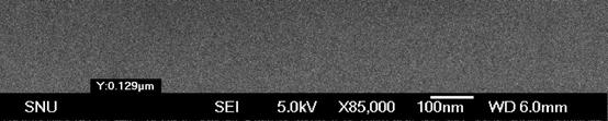
28 2.4 Characterization of RaDNA substrate To figure out the characterization of the SOG substrate, various measurements were performed. The images of RaDNA substrate were measured by optical microscope, atomic force microscope (AFM), scanning electron microscope (SEM). In addition to the images, the transmittance and the haze of the substrate were measured. Figure 2.3 shows the AFM image of the UV-curable resin RaDNA substrate whose pattern is almost reverse pattern of Si master mold. So the UV-curable resin RaDNA substrate has equal heights of nano-pillar. The AFM image SOG RaDNA after NIL is shown in Figure 2.4. The heights and the diameters of the SOG pillar were lower than the UV curable pillar s. During NIL, the SOG pillar heights were decreased due to the evaporation of solvents. Figure 2.5 shows AFM image of the SOG RaDNA substrate after annealing. Through annealing, the gel pillar was converted to the poly-crystalline SiO 2 pillar with densification and grain growth. Despite of the shrinkage of the pillar diameter, the average pillar height was remained as 225 nm during curing process. The shrinkage was taken up in the dimension mainly perpendicular to the surface [17]. The AFM image of the planarized substrate is in Figure 2.6. The mean pillar radius and roughness of substrates was obtained as in table 2. The R pv of RaDNA substrates before and after planarization were 299 nm and 243 nm. Figure 2.7 and Figure 2.8 show the optical microscope images of RaDNA substrates before and after planarization. Periodic 10 * 10 μm 2 random patterns can be seen in large area. The T75 didn t make substrate totally flat, 18
29 so nano-pattern also was shown in the planarized substrate. Instead of the rough surface, any crack was shown in the planarized substrate. The SEM images of the substrate before and after planarization are shown in Figure 2.9. Different material could be discerned by different electron back scattering. Fig 2.9 (a), around 300 nm of SOG thin layer was deposited on the glass substrate except pillar array. Around 140nm of the T75 thin film was coated on pillar array as shown in Fig 2.9 (b). The roughness of the planarized substrate was due to lower thickness of the T75 film than the height of the SOG pillar. To be applied in a display, the transmittance haze that is related with a pixel blurring is also key-factor to be considered. Figure 2.10 shows measurement system of transmittance haze. The transmittance haze is percent ratio of the diffused transmittance to the total transmittance in integrating sphere. The result of haze measurement with white light is shown in table 2.2. Higher pillar height has more capability of light-scattering so, had bigger haze. The haze of SOG substrate was lower than UV curable resin s due to lower pillar height. The hazes of RaDNA substrates before and after planarization were and Figure 2.11 (a) ~ (d) are photographs of text printed beneath different substrates (glass substrate, planarized SOG RaDNA substrate, UV curable resin substrate, microlens array on the glass substrate). Thickness of glass substrate is 0.64 mm. Texts beneath microlens array on substrate were blurred. While texts beneath planarized SOG RaDNA substrate were clear and it means SOG RaDNA substrate is more proper at a display. The transmittance of substrate is shown in Figure Because of light- 19
30 scattering, transmittance of RaDNA substrate was lower than transmittance of bare glass. Planarized RaDNA substrate had higher transmittance than RaDNA substrate at 480 ~ 520 nm, green light. 20


31 Figure 2.3 AFM image of RaDNA substrate fabricated using a UV curable resin. Figure 2.4 AFM image of SOG RaDNA substrate fabricated using SOG. 21


32 Figure 2.5 AFM image of SOG RaDNA substrate after curing at 400 C and vacuum for 1 hour. Figure 2.6 AFM image of SOG RaDNA substrate planarized by T75. 22
33 Table 2.2 Summary of area, volume, height, peak to valley of pillars. Substrate Average R pv R q R a radius (nm) (nm) (nm) (nm) RaDNA (UVcurable resin) RaDNA (SOG) RaDNA (SOG, cured.) RaDNA (SOG, planarized.)
34 Figure 2.7 Optical microscope image of RaDNA substrate at magnification of (a) x 500 and (b) x
35 Figure 2.8 Optical microscope image of planarized RaDNA substrate at magnification of (a) x 500 and (b) x


36 Figure 2.9 SEM images of RaDNA substrate before and after planarization. 26
 glass substrate, (b) planarized SOG RaDNA substrate, (c) UV curable resin substrate and (d)")
37 Figure 2.10 Schematic measurement system of transmittance haze in integrating sphere. Figure 2.11 Photographs of images througn (a) glass substrate, (b) planarized SOG RaDNA substrate, (c) UV curable resin substrate and (d) microlens array on the glass substrate. 27
38 Table 2.3 Haze and transmittance of RaDNA substrates with different material and height of pillar before and after planarization. Substrate Planarization Height of pillar Transmittance Haze Glass X UV curable resin X RaDNA substrate UV curable resin X RaDNA substrate UV curable resin X RaDNA substrate SOG RaDNA X substrate UV curable resin O RaDNA substrate UV curable resin O RaDNA substrate UV curable resin O RaDNA substrate SOG RaDNA O substrate 28
39 Transmittance (%) Glass substrate RaDNA substrate Planarized RaDNA substrate Wavelength (nm) Figure 2.12 Transmittance of glass and RaDNA substrate before and after planarization. 29
40 Chapter.3 Fabrication of RaDNA OLED 3.1 Device design of green phosphorescent OLED The OLED structure is highly efficient green phosphorescent device that was devised by Lu et al. [23]. In this device, using CBP as both HTL and EML, energy barrier between HTL/EML was eliminated. Nearly same Energy level of the ETL (TPBi) with the EML (CBP) made the device have good roll-off. In contrast to the original device, transparent electrode material is used as indium zinc oxide (IZO). Because transparent electrode has different refractive index and thickness, OLED device was re-designed to have a high efficiency. The optimization of device was performed with a classical electromagnetic theory developed by Chance, Prock and Silbey (CPS) [24, 25]. In simulation, device was modeled as a simple one dimensional (1D) weak micro-cavity which consists of glass, IZO, multi-layered organic and metal. The emission was assumed as isotropic sheet dipole radiation which is located in the center of the EML. Thickness of the HTL was systemically changed to watch power coupling ratios without changing thickness of other layers. The Schematic diagram of the device structure for optical modeling is shown in Figure 3.1. Figure 3.2 shows the simulation result from different HTL thickness. When the HTL thickness is 70 nm, 25% out-coupling efficiency was achieved. The fraction of internal absorption, surface plasma polariton (SPP), organic mode, 30
41 wave guide mode was 0.11, 0.11, 0.37 and, The SPP is absorption due to dipole decay near metal. Each material has imaginary refractive indices, 11% light is absorbed. Due to the high refractive indices of organic and IZO, 37% of generated light in device was captured still. Optimized device structure was IZO (70 nm) / MoO 3 (1 nm) / CBP (75 nm) / CBP : 8wt.% Ir(ppy) 2 (acac) (15 nm) / TPBi (60 nm) / LiF (1 nm) / Al (100 nm) 31


42 Figure 3.1 Schematic diagram of the device structure for optical modeling. Figure 3.2 Power coupling ratio of the dissipated power from emissive dipoles coupled to various optical modes. 32
43 3.2 Fabrication of green phosphorescent OLED The OLED was fabricated on the planarized RaDNA substrate as optimized device. The IZO was deposited by a facing target sputtering system at working pressure 2.5*10-3 Torr. The sheet resistance of the IZO was measured by 4-point probe and has 103 Ω/. Before the organic deposition, UV-O 3 treatment was done for 10 min on the IZO electrode to reduce the energy level of IZO. Organic materials were deposited by the thermal evaporation without breaking the vacuum at a pressure of < 5*10-7 Torr. The thickness of each layer was measured by a quartz crystal sensor. For comparison with conventional ITO device, ITO substrate also fabricated along with IZO device. A Keithley 2400 semiconductor parameter analyzer and a Photo Research PR- 650 spectrophotometer were used to measure the luminescent and electric characteristics, respectively. The integrating sphere with a photomultiplier was utilized for measurement of total extraction enhancement. 33

44 Figure 3.3 The structure of RaDNA OLED. 34
45 3.3 Result and Discussion The current density-voltage-luminance (J-V-L) diagram is shown in Figure 3.4. All devices have 3 V of turn-on voltage. That means OLED had been fabricated equally. In high voltage, current density of IZO device was lower than ITO device s due to high sheet resistance of IZO. The reason that the RaDNA OLED has high injection properties was roughness of the RaDNA substrate. The electrode on pillar was applied high electric field. That results in large current injection. Figure 3.5 shows luminance efficiency and power efficiency of reference and RaDNA device. The luminance efficiency at 2.5 ma/cm 2 are (reference) and (RaDNA) Cd/A. The power efficiency at 2.5 ma/cm 2 are (reference) and (RaDNA) lm/watt. The enhancement ratio of luminance efficiency and power efficiency were 1.07 (luminance efficiency) and 1.14 (power efficiency). Figure 3.6 shows the result of integrating sphere measurement at 2.5 ma/cm 2. The spectrum of both reference and RaDNA OLED were almost same. Overall enhancement ratio was larger in integrating sphere. It was inferred that lights of high angle at normal direction were extracted more. The increase of glass mode of light was inferred from larger enhancement at high angle. The enhancement ratio of each wavelength is shown in Figure 3.7. The electroluminescence (EL) intensity at edge sides was so low that the enhancement at both sides can t be accepted as it shows. In contrast to the PC OLED, the enhancement ratio was equal at each wavelength. It means the 35
46 RaDNA OLED shows any color-shift. Overall enhancement ratio has lower value than hexagonal PC OLED s. PC OLED was optimized to enhance light of specific wavelength. In contrast to variation with viewing angle of PC OLED, RaDNA OLED has equal emission pattern. 36
47 Current Density (ma/cm 2 ) 2.0x x x x10 0 IZO reference RaDNA OLED ITO reference Luminance Voltage (V) Figure 3.4 Current density-voltage-luminance characteristics Luminance (cd/m 2 ) Luminance efficiency (cd/a) IZO reference Power efficiency 20 RaDNA OLED Current density (ma/cm 2 ) Power efficiency (lm/w) Figure 3.5 Luminance and power efficiency curve. 37
48 1.5 Ref RaDNA EL intensity (a.u.) Wavelength (nm) Figure 3.6 The EL intensity at integrating sphere. 2.0 Enhancement ratio Wavelength (nm) Figure 3.7 Enhancement ratios at wavelength 38
49 Chapter.4 Conclusion The RaDNA substrate was fabricated with the spin-on glass. The fabrication method was simple with the RT-NIL. The trialkoxysilane-capped PMMA-titania hybrid optical material was used as planarization layer, decreasing peak to valley 299 nm to 243 nm and had no crack. The planarized substrate showed haze less than 10. The optimized OLED was designed with CPS simulation which is based on the classical electromagnetic theory. The RaDNA OLED has 7% efficiency enhancement at normal direction and 19% enhancement in integrating sphere. The emission pattern didn t show any variation with azimuthal angle. 39
50 References [1] S.R. Forrest, D.D.C. Bradley, M.E. Thomson, Adv. Mater. 15, 1043 (2003). [2] N.K. Patel, S. Cinà, J.H. Burroughes, IEEE J. on Selected Topics in Quantum Electronics, 8, 346 (2002). [3] Y.-H. Cheng, J.-L. Wu, C.-H. Cheng, K.-C. Syao and M.-C. M. Lee, Appl. Phys. Lett. 90, (2007). [4] S. Möller and S. R. Forrest, J. Appl. Phys. 91, 3324 (2002). [5] Y.-R. Do, Y.-C. Kim, Y.-W. Song, C.-O. Cho, H. Jeon, Y.-J. Lee, S.-H. Kim and Y.-H. Lee, Adv. Mater. 15, 1214 (2003). [6] Y.-C. Kim, S.-H. Cho, Y.-W. Song, Y.-J. Lee, Y.-H. Lee, Y. -R. Do, Appl. Phys. Lett. 89, (2006). [7] S.-H. Jeon, J.-W. Kang, H.-D. Park, Jang-Joo Kim, J.-R. Youn, J.- Y Shim, J.-H Jeong, D.-G. Choi, K.-D. Kim, A. O. Altun, S.-H. Kim, and Y.-H. Lee, Appl. Phys. Lett. 92, (2008). [8] H.-H. Cho, B.-I. Park, H.-J. Kim, J.-Y. Shim, S.-H. Jeon, J.-H. Jeong, J.-J. Kim, Curr. Appl. Phys. 10, e139 (2010). [9] Y. Sun and S. R. Forrest, Nat. Photonics, 2, 483 (2008). [10] S.A. Choulis, M.K. Mathai, and V.E. Choong, Appl. Phys. Lett. 88, (2006). [11] A. Kumar, R. Srivastava, M. N. Kamalasanan, and D. S. Mehta, Opt. Lett. 37, 575 (2012). [12] T. Yamasaki, K. Sumioka, T. Tsutsui, Appl. Phys. Lett. 76, 1243 (2000). [13] Y.-J. Lee, S.-H. Kim, G.-H. Kim, Y.-H. Lee, S.-H. Cho, Y.-W. Song, Y.-C. Kim, Y.-R. Do, Opt. Express 13, 5864 (2005). 40
51 [14] H.-H. Cho, mater thesis, SNU (2009). [15] B.-I. Park, mater thesis, SNU (2011). [16] N. N. Toan, thesis, University of Twente (1999). [17] L. J. Guo, Adv. Mater. 19, 495, (2007). [18] Y. Kang, M. Okada, C. Minari, K. Kanda, Y. Haruyama and S. Matsui, Jpn J. Appl. Phys. 49, 06GL13 (2010). [19] Y. Xia and G. M. Whitesides, Angew. Chem. Int. Ed. 37, 550 (1998). [20] K.-Y. Yang, S.-C. Oh, H. Park, and H. Lee, J. Vac. Sci. Technol. B 29, (2011). [21] H.-C. Scheer, W. Häfner, A. Fidler, S. Möllenbeck, and N. Bogdanski, J. Vac. Sci. Technol. B, 26(6), 2380 (2008). [22] L.-H. Lee and W.-C. Chen, Chem. Mater. 13, 1137 (2001). [23] Z. B. Wang, M. G. Helander, J. Qiu, D. P. Puzzo, M. T. Greiner, Z. W. Liu and Z. H. Lu, Appl. Phys. Lett. 98, (2011). [24] R. R. Chance, A. Prock, R. Silbey, Adv. Chem. Phys. 37, 1 (1987). [25] S.-Y. Kim and J.-J. Kim, Org. Electron. 11, 1010, (2010). 41
52 초 록 차세대디스플레이재료로각광받는유기발광소자 (OLED) 는내부물질의높은굴절률로인해약 75% 의빛이소자밖으로나오지못하고소멸된다. 내부에갇힌빛을추출하는방법중하나인광결정을투명전극과유리기판사이에삽입하는방식은, 광결정의주기적배열때문에특정방향으로빛이추출되는단점을가지고있다. 이를개선하기위해광결정대신비주기적나노구조를삽입하였다. 또한나노구조의재료로안정한무기물인스핀온글라스를나노임프린트리소그래피공정으로제작하였다. 균일한패턴제작을위해폴리다이메틸실록세인몰드위에스핀온글라스를먼저올린나노트랜스퍼리소그래피를사용하였다. 폴리머-무기하이브리드필름을스핀코팅으로입혀서기판을평탄화하였다. 소자는정면방향에서 7%, 적분구측정으로 19% 의효율증가를보였다. 파장전반적인광추출효율을보였고, 방위각에따른소자의발광패턴은동일하였다. 주요어 : 유기발광다이오드, 비주기적나노구조, 상온나노임프린트리소그래피, 스핀온글라스, 폴리머-무기하이브리드필름학번 :
Light Extraction in OLED with Corrugated Substrates Franky So
 Light Extraction in OLED with Corrugated Substrates Franky So Department of Materials Science and Engineering North Carolina State University Raleigh, NC 27695-7907 1 Where Did the Light Go? Modes Distribution
CURRENT STATUS OF NANOIMPRINT LITHOGRAPHY DEVELOPMENT IN CNMM
 U.S. -KOREA Forums on Nanotechnology 1 CURRENT STATUS OF NANOIMPRINT LITHOGRAPHY DEVELOPMENT IN CNMM February 17 th 2005 Eung-Sug Lee,Jun-Ho Jeong Korea Institute of Machinery & Materials U.S. -KOREA Forums
Inverted top-emitting organic light-emitting diodes using transparent conductive NiO electrode
 Applied Surface Science 244 (2005) 439 443 www.elsevier.com/locate/apsusc Inverted top-emitting organic light-emitting diodes using transparent conductive NiO electrode Se-W. Park a, Jeong-M. Choi a, Eugene
Supplementary Information. Light Manipulation for Organic Optoelectronics Using Bio-inspired Moth's Eye. Nanostructures
 Supplementary Information Light Manipulation for Organic Optoelectronics Using Bio-inspired Moth's Eye Nanostructures Lei Zhou, Qing-Dong Ou, Jing-De Chen, Su Shen, Jian-Xin Tang,* Yan-Qing Li,* and Shuit-Tong
SUPPORTING INFORMATION
 SUPPORTIG IFORMATIO [1,2,4]Triazolo[1,5-a]pyridine-based Host Materials for Green Phosphorescent and Delayed-Fluorescence OLEDs with Low Efficiency Roll-off Wenxuan Song, a Yi Chen, a Qihao Xu, a Haichuan
Making OLEDs efficient
 Making OLEDs efficient cathode anode light-emitting layer η = γ EL r ηpl k st External Efficiency Outcoupling Internal efficiency of LEDs η = γ EL r ηpl k st γ = excitons formed per charge flowing in the
REDUCED GRAPHITE OXIDE-INDIUM TIN OXIDE COMPOSITES FOR TRANSPARENT ELECTRODE USING SOLUTION PROCESS
 18 TH INTERNATIONAL CONFERENCE ON COMPOSITE MATERIALS REDUCED GRAPHITE OXIDE-INDIUM TIN OXIDE COMPOSITES FOR TRANSPARENT ELECTRODE USING SOLUTION PROCESS K. S. Choi, Y. Park, K-.C. Kwon, J. Kim, C. K.
Introduction. Fang-Chung Chen Department of Photonics and Display Institute National Chiao Tung University. Organic light-emitting diodes
 rganic light-emitting diodes Introduction Fang-Chung Chen Department of Photonics and Display Institute National Chiao Tung University rganic light-emitting diodes --The emerging technology LED Displays
Biologically Inspired Organic Light-Emitting Diodes
 Supporting Information Biologically Inspired Organic Light-Emitting Diodes Jae-Jun Kim,, Jaeho Lee, Sung-Pyo Yang, Ha Gon Kim, Hee-Seok Kweon ǁ, Seunghyup Yoo, and Ki-Hun Jeong*, Department of Bio and
Enhancing the Performance of Organic Thin-Film Transistor using a Buffer Layer
 Proceedings of the 9th International Conference on Properties and Applications of Dielectric Materials July 19-23, 29, Harbin, China L-7 Enhancing the Performance of Organic Thin-Film Transistor using
56.2: Invited Paper: Pixel-Isolated Liquid Crystal Mode for Plastic Liquid Crystal Displays
 56.2: Invited Paper: Pixel-Isolated Liquid Crystal Mode for Plastic Liquid Crystal Displays Jong-Wook Jung, Se-Jin Jang, Min Young Jin, You-Jin Lee, Hak-Rin Kim, and Jae-Hoon Kim Department of Electronics
Plastic Electronics. Joaquim Puigdollers.
 Plastic Electronics Joaquim Puigdollers Joaquim.puigdollers@upc.edu Nobel Prize Chemistry 2000 Origins Technological Interest First products.. MONOCROMATIC PHILIPS Today Future Technological interest Low
Supporting Information
 Electronic Supplementary Material (ESI) for Journal of Materials Chemistry C. This journal is The Royal Society of Chemistry 2017 Supporting Information Bicolour electroluminescence of 2 (carbazol 9 yl)anthraquinone
Supporting Information: Poly(dimethylsiloxane) Stamp Coated with a. Low-Surface-Energy, Diffusion-Blocking,
 Stamp Coated with a. Low-Surface-Energy, Diffusion-Blocking,") Supporting Information: Poly(dimethylsiloxane) Stamp Coated with a Low-Surface-Energy, Diffusion-Blocking, Covalently Bonded Perfluoropolyether Layer and Its Application to the Fabrication of Organic Electronic
Supporting Information: Poly(dimethylsiloxane) Stamp Coated with a Low-Surface-Energy, Diffusion-Blocking, Covalently Bonded Perfluoropolyether Layer and Its Application to the Fabrication of Organic Electronic
High-Performance Photocoupler Based on Perovskite Light Emitting Diode and Photodetector
 Supporting information for High-Performance Photocoupler Based on Perovskite Light Emitting Diode and Photodetector Zhi-Xiang Zhang, Ji-Song Yao, Lin Liang, Xiao-Wei Tong, Yi Lin, Feng-Xia Liang, *, Hong-Bin
E L E C T R O P H O S P H O R E S C E N C E
 Organic LEDs part 4 E L E C T R O P H O S P H O R E S C E C E. OLED efficiency 2. Spin 3. Energy transfer 4. Organic phosphors 5. Singlet/triplet ratios 6. Phosphor sensitized fluorescence 7. Endothermic
Color-Stable and Low-Roll-Off Fluorescent White Organic Light Emitting Diodes Based on Nondoped Ultrathin Emitters
 Copyright 5 by American Scientific Publishers All rights reserved. Printed in the United States of America Science of Advanced Materials Vol. 7, pp., 5 www.aspbs.com/sam Color-Stable and Low-Roll-Off Fluorescent
ORGANIC SEMICONDUCTOR 3,4,9,10-Perylenetetracarboxylic dianhydride (PTCDA)
") ORGANIC SEMICONDUCTOR 3,4,9,10-Perylenetetracarboxylic dianhydride (PTCDA) Suvranta Tripathy Department of Physics University of Cincinnati Cincinnati, Ohio 45221 March 8, 2002 Abstract In the last decade
ORGANIC SEMICONDUCTOR 3,4,9,10-Perylenetetracarboxylic dianhydride (PTCDA) Suvranta Tripathy Department of Physics University of Cincinnati Cincinnati, Ohio 45221 March 8, 2002 Abstract In the last decade
Three Approaches for Nanopatterning
 Three Approaches for Nanopatterning Lithography allows the design of arbitrary pattern geometry but maybe high cost and low throughput Self-Assembly offers high throughput and low cost but limited selections
Nanostrukturphysik (Nanostructure Physics)
") Nanostrukturphysik (Nanostructure Physics) Prof. Yong Lei & Dr. Yang Xu Fachgebiet 3D-Nanostrukturierung, Institut für Physik Contact: yong.lei@tu-ilmenau.de; yang.xu@tu-ilmenau.de Office: Unterpoerlitzer
Nanostrukturphysik (Nanostructure Physics) Prof. Yong Lei & Dr. Yang Xu Fachgebiet 3D-Nanostrukturierung, Institut für Physik Contact: yong.lei@tu-ilmenau.de; yang.xu@tu-ilmenau.de Office: Unterpoerlitzer
UNIT 3. By: Ajay Kumar Gautam Asst. Prof. Dev Bhoomi Institute of Technology & Engineering, Dehradun
 UNIT 3 By: Ajay Kumar Gautam Asst. Prof. Dev Bhoomi Institute of Technology & Engineering, Dehradun 1 Syllabus Lithography: photolithography and pattern transfer, Optical and non optical lithography, electron,
Quantum Dots for Advanced Research and Devices
 Quantum Dots for Advanced Research and Devices spectral region from 450 to 630 nm Zero-D Perovskite Emit light at 520 nm ABOUT QUANTUM SOLUTIONS QUANTUM SOLUTIONS company is an expert in the synthesis
High Performance, Low Operating Voltage n-type Organic Field Effect Transistor Based on Inorganic-Organic Bilayer Dielectric System
 Journal of Physics: Conference Series PAPER OPEN ACCESS High Performance, Low Operating Voltage n-type Organic Field Effect Transistor Based on Inorganic-Organic Bilayer Dielectric System To cite this
Flexible Organic Photovoltaics Employ laser produced metal nanoparticles into the absorption layer 1. An Introduction
 Flexible Organic Photovoltaics Employ laser produced metal nanoparticles into the absorption layer 1. An Introduction Among the renewable energy sources that are called to satisfy the continuously increased
Efficient light emission from LEDs, OLEDs, and nanolasers via surface-plasmon resonance
 Efficient light emission from LEDs, OLEDs, and nanolasers via surface-plasmon resonance Seok Ho Song, Hanyang University, http://optics.anyang.ac.kr/~shsong silver grating Key notes 1. How does the surface
A Photonic Crystal Laser from Solution Based. Organo-Lead Iodide Perovskite Thin Films
 SUPPORTING INFORMATION A Photonic Crystal Laser from Solution Based Organo-Lead Iodide Perovskite Thin Films Songtao Chen 1, Kwangdong Roh 2, Joonhee Lee 1, Wee Kiang Chong 3,4, Yao Lu 5, Nripan Mathews
Ultrafast single photon emitting quantum photonic structures. based on a nano-obelisk
 Ultrafast single photon emitting quantum photonic structures based on a nano-obelisk Je-Hyung Kim, Young-Ho Ko, Su-Hyun Gong, Suk-Min Ko, Yong-Hoon Cho Department of Physics, Graduate School of Nanoscience
Lithography-Free Broadband Ultrathin Film. Photovoltaics
 Supporting Information Lithography-Free Broadband Ultrathin Film Absorbers with Gap Plasmon Resonance for Organic Photovoltaics Minjung Choi 1, Gumin Kang 1, Dongheok Shin 1, Nilesh Barange 2, Chang-Won
Organic LEDs part 6. Exciton Recombination Region in Organic LEDs. Handout: Bulovic, et al., Chem. Phys. Lett. 287, 455 (1998); 308, 317 (1999).
; 308, 317 (1999).") Organic LEDs part 6 Exciton Recombination Region in Organic LEDs White OLED Flexible OLEDs Solvation Effect Solid State Solvation Handout: Bulovic, et al., Chem. Phys. Lett. 287, 455 (1998); 308, 317 (1999).
Organic LEDs part 6 Exciton Recombination Region in Organic LEDs White OLED Flexible OLEDs Solvation Effect Solid State Solvation Handout: Bulovic, et al., Chem. Phys. Lett. 287, 455 (1998); 308, 317 (1999).
Plasmonic Hot Hole Generation by Interband Transition in Gold-Polyaniline
 Supplementary Information Plasmonic Hot Hole Generation by Interband Transition in Gold-Polyaniline Tapan Barman, Amreen A. Hussain, Bikash Sharma, Arup R. Pal* Plasma Nanotech Lab, Physical Sciences Division,
Multicolor Graphene Nanoribbon/Semiconductor Nanowire. Heterojunction Light-Emitting Diodes
 Multicolor Graphene Nanoribbon/Semiconductor Nanowire Heterojunction Light-Emitting Diodes Yu Ye, a Lin Gan, b Lun Dai, *a Hu Meng, a Feng Wei, a Yu Dai, a Zujin Shi, b Bin Yu, a Xuefeng Guo, b and Guogang
Title of file for HTML: Supplementary Information Description: Supplementary Figures and Supplementary References
 Title of file for HTML: Supplementary Information Description: Supplementary Figures and Supplementary References Supplementary Figure 1. SEM images of perovskite single-crystal patterned thin film with
Techniken der Oberflächenphysik (Techniques of Surface Physics)
") Techniken der Oberflächenphysik (Techniques of Surface Physics) Prof. Yong Lei & Dr. Yang Xu (& Liying Liang) Fachgebiet 3D-Nanostrukturierung, Institut für Physik Contact: yong.lei@tu-ilmenau.de; yang.xu@tu-ilmenau.de;
Techniken der Oberflächenphysik (Techniques of Surface Physics) Prof. Yong Lei & Dr. Yang Xu (& Liying Liang) Fachgebiet 3D-Nanostrukturierung, Institut für Physik Contact: yong.lei@tu-ilmenau.de; yang.xu@tu-ilmenau.de;
Highly Efficient Orange Electrophosphorescence from a Trifunctional Organoboron-Pt(II) Complex
 Complex") Supporting Information Highly Efficient Orange Electrophosphorescence from a Trifunctional Organoboron-Pt(II) Complex Zachary M. Hudson, Michael G. Helander, Zheng-Hong Lu and Suning Wang S1. General Experimental
Supporting Information Highly Efficient Orange Electrophosphorescence from a Trifunctional Organoboron-Pt(II) Complex Zachary M. Hudson, Michael G. Helander, Zheng-Hong Lu and Suning Wang S1. General Experimental
Flexible nonvolatile polymer memory array on
 Supporting Information for Flexible nonvolatile polymer memory array on plastic substrate via initiated chemical vapor deposition Byung Chul Jang, #a Hyejeong Seong, #b Sung Kyu Kim, c Jong Yun Kim, a
Atmospheric pressure Plasma Enhanced CVD for large area deposition of TiO 2-x electron transport layers for PV. Heather M. Yates
 Atmospheric pressure Plasma Enhanced CVD for large area deposition of TiO 2-x electron transport layers for PV Heather M. Yates Why the interest? Perovskite solar cells have shown considerable promise
Supplementary Information
 Enhanced Electroluminescence from a Thiophene-Based Insulated Molecular Wire Gábor Méhes,,,# Chengjun Pan,, Fatima Bencheikh, Li Zhao, Kazunori Sugiyasu, *, Masayuki Takeuchi, Jean-Charles Ribierre, *,,
Enhancement of Light Outcoupling Efficiency in OLEDs
 Enhancement of Light Outcoupling Efficiency in OLEDs Stéphane Altazin*, Lidia Stepanova*, Lieven Penninck*, Christoph Kirsch**, Beat Ruhstaller** *Fluxim AG, Winterthur, Switzerland **Zurich University
Light manipulation in organic light-emitting devices by integrating micro/nano patterns
 Laser Photonics Rev., 1600145 (2017) / DOI 10.1002/lpor.201600145 LASER The demonstration of high efficiency and color tunability has brought organic light-emitting devices (OLEDs) into the lighting and
Super Flexible, High-efficiency Perovskite Solar Cells Employing Graphene Electrodes: Toward Future Foldable Power Sources
 Electronic Supplementary Material (ESI) for Energy & Environmental Science. This journal is The Royal Society of Chemistry 2016 Electronic Supplementary Information Super Flexible, High-efficiency Perovskite
λ = 550 nm n org = 1.8 High-index layer (n H d H = λ/4) Glass for n H =λ/4 (nm) d H Calculated EQE (%) (%) d org : 150 nm
 Glass for n H =λ/4 (nm) d H Calculated EQE (%) (%) d org : 150 nm") a Al d dipole : 70 nm from Al Emitter : Ir(ppy) 2 acac n org = 1.8 R bot d org : 150 nm 4-layer graphene High-index layer (n H d H = λ/4) Glass R bot (%) b 40 35 30 25 20 15 10 5 0 d H for n H d H =λ/4
a Al d dipole : 70 nm from Al Emitter : Ir(ppy) 2 acac n org = 1.8 R bot d org : 150 nm 4-layer graphene High-index layer (n H d H = λ/4) Glass R bot (%) b 40 35 30 25 20 15 10 5 0 d H for n H d H =λ/4
Stretchable Graphene Transistors with Printed Dielectrics and Gate Electrodes
 Stretchable Graphene Transistors with Printed Dielectrics and Gate Electrodes Seoung-Ki Lee, Beom Joon Kim, Houk Jang, Sung Cheol Yoon, Changjin Lee, Byung Hee Hong, John A. Rogers, Jeong Ho Cho, Jong-Hyun
MSN551 LITHOGRAPHY II
 MSN551 Introduction to Micro and Nano Fabrication LITHOGRAPHY II E-Beam, Focused Ion Beam and Soft Lithography Why need electron beam lithography? Smaller features are required By electronics industry:
Electronic Supplementary Information
 Electronic Supplementary Material (ESI) for ChemComm. This journal is The Royal Society of Chemistry 2018 Electronic Supplementary Information Room-Temperature Film Formation of Metal Halide Perovskites
A. Optimizing the growth conditions of large-scale graphene films
 1 A. Optimizing the growth conditions of large-scale graphene films Figure S1. Optical microscope images of graphene films transferred on 300 nm SiO 2 /Si substrates. a, Images of the graphene films grown
Enhanced Light Extraction from Organic Light Emitting Diodes by Micrometer-Sized Buckles
 Copyright 2014 American Scientific Publishers All rights reserved Printed in the United States of America Article Journal of Nanoscience and Nanotechnology Vol. 14, 8231 8236, 2014 www.aspbs.com/jnn Enhanced
Nanotechnology Fabrication Methods.
 Nanotechnology Fabrication Methods. 10 / 05 / 2016 1 Summary: 1.Introduction to Nanotechnology:...3 2.Nanotechnology Fabrication Methods:...5 2.1.Top-down Methods:...7 2.2.Bottom-up Methods:...16 3.Conclusions:...19
Supporting Information
 Supporting Information Modulation of PEDOT:PSS ph for Efficient Inverted Perovskite Solar Cells with Reduced Potential Loss and Enhanced Stability Qin Wang 1,2, Chu-Chen Chueh 1, Morteza Eslamian 2 * and
Exceptionally efficient organic light emitting devices using high refractive index substrates
 Exceptionally efficient organic light emitting devices using high refractive index s Saso Mladenovski, 1,* Kristiaan Neyts, 1 Domagoj Pavicic, 2 Ansgar Werner 2 and Carsten Rothe 2 1 Electronics and Information
Nanoimprint Lithography
 Nanoimprint Lithography Wei Wu Quantum Science Research Advanced Studies HP Labs, Hewlett-Packard Email: wei.wu@hp.com Outline Background Nanoimprint lithography Thermal based UV-based Applications based
PHYSICS nd TERM Outline Notes (continued)
") PHYSICS 2800 2 nd TERM Outline Notes (continued) Section 6. Optical Properties (see also textbook, chapter 15) This section will be concerned with how electromagnetic radiation (visible light, in particular)
PHYSICS 2800 2 nd TERM Outline Notes (continued) Section 6. Optical Properties (see also textbook, chapter 15) This section will be concerned with how electromagnetic radiation (visible light, in particular)
Photovoltaic Enhancement Due to Surface-Plasmon Assisted Visible-Light. Absorption at the Inartificial Surface of Lead Zirconate-Titanate Film
 Photovoltaic Enhancement Due to Surface-Plasmon Assisted Visible-Light Absorption at the Inartificial Surface of Lead Zirconate-Titanate Film Fengang Zheng, a,b, * Peng Zhang, a Xiaofeng Wang, a Wen Huang,
Enhanced Transmission by Periodic Hole. Arrays in Metal Films
 Enhanced Transmission by Periodic Hole Arrays in Metal Films K. Milliman University of Florida July 30, 2008 Abstract Three different square periodic hole arrays were manufactured on a silver film in order
Low Power Phase Change Memory via Block Copolymer Self-assembly Technology
 Low Power Phase Change Memory via Block Copolymer Self-assembly Technology Beom Ho Mun 1, Woon Ik Park 1, You Yin 2, Byoung Kuk You 1, Jae Jin Yun 1, Kung Ho Kim 1, Yeon Sik Jung 1*, and Keon Jae Lee 1*
Supporting Information. Fast Synthesis of High-Performance Graphene by Rapid Thermal Chemical Vapor Deposition
 1 Supporting Information Fast Synthesis of High-Performance Graphene by Rapid Thermal Chemical Vapor Deposition Jaechul Ryu, 1,2, Youngsoo Kim, 4, Dongkwan Won, 1 Nayoung Kim, 1 Jin Sung Park, 1 Eun-Kyu
Supporting Information
 Supporting Information Assembly and Densification of Nanowire Arrays via Shrinkage Jaehoon Bang, Jonghyun Choi, Fan Xia, Sun Sang Kwon, Ali Ashraf, Won Il Park, and SungWoo Nam*,, Department of Mechanical
Supplementary Information. High-Performance, Transparent and Stretchable Electrodes using. Graphene-Metal Nanowire Hybrid Structures
 Supplementary Information High-Performance, Transparent and Stretchable Electrodes using Graphene-Metal Nanowire Hybrid Structures Mi-Sun Lee, Kyongsoo Lee, So-Yun Kim, Heejoo Lee, Jihun Park, Kwang-Hyuk
Supplementary Figure 1 shows overall fabrication process and detailed illustrations are given
 Supplementary Figure 1. Pressure sensor fabrication schematics. Supplementary Figure 1 shows overall fabrication process and detailed illustrations are given in Methods section. (a) Firstly, the sacrificial
Supplementary Figures Supplementary Figure 1
 Supplementary Figures Supplementary Figure 1 Optical images of graphene grains on Cu after Cu oxidation treatment at 200 for 1m 30s. Each sample was synthesized with different H 2 annealing time for (a)
Control of Polymer Structures in Phase-Separated Liquid Crystal-Polymer Composite Systems
 Japanese Journal of Applied Physics Vol. 44, No. 5A, 2005, pp. 3115 3120 #2005 The Japan Society of Applied Physics Control of Polymer Structures in Phase-Separated Liquid Crystal-Polymer Composite Systems
Emission pattern control and polarized light emission through patterned graded-refractiveindex coatings on GaInN light-emitting diodes
 Emission pattern control and polarized light emission through patterned graded-refractiveindex coatings on GaInN light-emitting diodes Ming Ma, 1 Ahmed N. Noemaun, 2 Jaehee Cho, 2,* E. Fred Schubert, 2
(Co-PIs-Mark Brongersma, Yi Cui, Shanhui Fan) Stanford University. GCEP Research Symposium 2013 Stanford, CA October 9, 2013
 Stanford University. GCEP Research Symposium 2013 Stanford, CA October 9, 2013") High-efficiency thin film nano-structured multi-junction solar James S. cells Harris (PI) (Co-PIs-Mark Brongersma, Yi Cui, Shanhui Fan) Stanford University GCEP Research Symposium 2013 Stanford, CA October
High-efficiency thin film nano-structured multi-junction solar James S. cells Harris (PI) (Co-PIs-Mark Brongersma, Yi Cui, Shanhui Fan) Stanford University GCEP Research Symposium 2013 Stanford, CA October
Supplementary Figure 1 Detailed illustration on the fabrication process of templatestripped
 Supplementary Figure 1 Detailed illustration on the fabrication process of templatestripped gold substrate. (a) Spin coating of hydrogen silsesquioxane (HSQ) resist onto the silicon substrate with a thickness
Hysteresis-free low-temperature-processed planar perovskite solar cells with 19.1% efficiency
 Electronic Supplementary Material (ESI) for Energy & Environmental Science. This journal is The Royal Society of Chemistry 2016 Supplementary Information Hysteresis-free low-temperature-processed planar
Structure Property Relationships of. Organic Light-Emitting Diodes. Michael Kochanek May 19, 2006 MS&E 542 Flexible Electronics
 Structure Property Relationships of Organic Light-Emitting Diodes Michael Kochanek May 19, 2006 MS&E 542 Flexible Electronics Introduction Many of today s solid-state inorganic microelectronic devices
Chandigarh, India
 Efficiency Enhancement of Graphene based flexible Organic light emitting diodes Rita Rana, Rajesh Mehra 1,2 National Institute of Technical Teachers Training and Research, Electronics and Communication,
Supplementary Figure 1. Potential energy, volume, and molecular distribution of the
 1 2 3 4 5 6 7 8 Supplementary Figure 1. Potential energy, volume, and molecular distribution of the organic substrates prepared by MD simulation. (a) Change of the density and total potential energy of
Nanostructures Fabrication Methods
 Nanostructures Fabrication Methods bottom-up methods ( atom by atom ) In the bottom-up approach, atoms, molecules and even nanoparticles themselves can be used as the building blocks for the creation of
Three-dimensional flexible and conductive interconnected graphene networks grown by chemical vapour deposition
 SUPPLEMENTARY INFORMATION Three-dimensional flexible and conductive interconnected graphene networks grown by chemical vapour deposition S1. Characterization of the graphene foam (GF) and GF/PDMS composites
Because light behaves like a wave, we can describe it in one of two ways by its wavelength or by its frequency.
 Light We can use different terms to describe light: Color Wavelength Frequency Light is composed of electromagnetic waves that travel through some medium. The properties of the medium determine how light
Seminars in Nanosystems - I
 Seminars in Nanosystems - I Winter Semester 2011/2012 Dr. Emanuela Margapoti Emanuela.Margapoti@wsi.tum.de Dr. Gregor Koblmüller Gregor.Koblmueller@wsi.tum.de Seminar Room at ZNN 1 floor Topics of the
Spiro-Configured Bifluorenes: Highly Efficient Emitter for UV Organic Light-Emitting Device and Host Material for Red Electrophosphorescence
 Spiro-Configured Bifluorenes: Highly Efficient Emitter for UV Organic Light-Emitting Device and Host Material for Red Electrophosphorescence Ken-Tsung Wong,* a Yuan-Li Liao, a Yu-Ting Lin, b Hai-Ching
Supporting Information
 Electronic Supplementary Material (ESI) for Journal of Materials Chemistry A. This journal is The Royal Society of Chemistry 2015 Supporting Information 1. Synthesis of perovskite materials CH 3 NH 3 I
Supporting Information. Direct Growth of Graphene Films on 3D Grating. Structural Quartz Substrates for High-performance. Pressure-Sensitive Sensor
 Supporting Information Direct Growth of Graphene Films on 3D Grating Structural Quartz Substrates for High-performance Pressure-Sensitive Sensor Xuefen Song, a,b Tai Sun b Jun Yang, b Leyong Yu, b Dacheng
Supporting Information
 Supporting Information Oh et al. 10.1073/pnas.0811923106 SI Text Hysteresis of BPE-PTCDI MW-TFTs. Fig. S9 represents bidirectional transfer plots at V DS 100VinN 2 atmosphere for transistors constructed
Improvement of MgO Characteristics Using RF-Plasma Treatment in AC Plasma Display Panel
 Mol. Cryst. Liq. Cryst., Vol. 531: pp. 73=[373] 81=[381], 2010 Copyright # Taylor & Francis Group, LLC ISSN: 1542-1406 print=1563-5287 online DOI: 10.1080/15421406.2010.499331 Improvement of MgO Characteristics
High contrast tandem organic light emitting devices
 Edith Cowan University Research Online ECU Publications 2012 2012 High contrast tandem organic light emitting devices Baofu Ding Edith Cowan University Xiao-Yuan Hou Kamal Alameh Edith Cowan University
Nanocomposite photonic crystal devices
 Nanocomposite photonic crystal devices Xiaoyong Hu, Cuicui Lu, Yulan Fu, Yu Zhu, Yingbo Zhang, Hong Yang, Qihuang Gong Department of Physics, Peking University, Beijing, P. R. China Contents Motivation
Nanomaterials and their Optical Applications
 Nanomaterials and their Optical Applications Winter Semester 2013 Lecture 02 rachel.grange@uni-jena.de http://www.iap.uni-jena.de/multiphoton Lecture 2: outline 2 Introduction to Nanophotonics Theoretical
Supporting Information
 Supporting Information A New Molecular Design Based on Thermally Activated Delayed Fluorescence for Highly Efficient Organic Light Emitting Diodes Pachaiyappan Rajamalli, Natarajan Senthilkumar, Parthasarathy
Inverted Quantum-dot Light-Emitting Diode with Solution-Processed Aluminum-Zinc- Oxide as Cathode Buffer
 Normalized Absorbance (a.u.) Normalized PL Intensity (a.u.) Electronic Supplementary Material (ESI) for Journal of Materials Chemistry C This journal is The Royal Society of Chemistry 22 SUPPORTING INFORMATION
Supporting Information
 Supporting Information Band Gap Tuning of CH 3 NH 3 Pb(Br 1-x Cl x ) 3 Hybrid Perovskite for Blue Electroluminescence Naresh K. Kumawat 1, Amrita Dey 1, Aravindh Kumar 2, Sreelekha P. Gopinathan 3, K.
Supplementary Figure 1 XRD pattern of a defective TiO 2 thin film deposited on an FTO/glass substrate, along with an XRD pattern of bare FTO/glass
 Supplementary Figure 1 XRD pattern of a defective TiO 2 thin film deposited on an FTO/glass substrate, along with an XRD pattern of bare FTO/glass and a reference pattern of anatase TiO 2 (JSPDS No.: 21-1272).
Overview of the main nano-lithography techniques
 Overview of the main nano-lithography techniques Soraya Sangiao sangiao@unizar.es Outline Introduction: Nanotechnology. Nano-lithography techniques: Masked lithography techniques: Photolithography. X-ray
Electronic Supplementary information (ESI) for. High-Performance Electrothermal and Anticorrosive Transparent
 for. High-Performance Electrothermal and Anticorrosive Transparent") Electronic Supplementary Material (ESI) for Journal of Materials Chemistry A. This journal is The Royal Society of Chemistry 2018 Electronic Supplementary information (ESI) for High-Performance Electrothermal
Electronic Supplementary Material (ESI) for Journal of Materials Chemistry A. This journal is The Royal Society of Chemistry 2018 Electronic Supplementary information (ESI) for High-Performance Electrothermal
Temperature Dependent Current-voltage Characteristics of P- type Crystalline Silicon Solar Cells Fabricated Using Screenprinting
 Temperature Dependent Current-voltage Characteristics of P- type Crystalline Silicon Solar Cells Fabricated Using Screenprinting Process Hyun-Jin Song, Won-Ki Lee, Chel-Jong Choi* School of Semiconductor
Supporting Information. Monolithic perovskite-homojunction silicon tandem solar cell with over 22% efficiency
 Electronic Supplementary Material (ESI) for Energy & Environmental Science. This journal is The Royal Society of Chemistry 2017 Electronic Supplementary Information (ESI) for Energy & Environmental Science
Next Generation Hole Injection/Transport Nano-Composites for High Efficiency OLED Development
 Next Generation Hole Injection/Transport Nano-Composites for High Efficiency OLED Development Sponsored by Solid State Lighting Core Technology Program Department of Energy Agiltron, Inc. Final Technical
ABSTRACT 1. INTRODUCTION 2. EXPERIMENT
 Fabrication of Nanostructured Heterojunction LEDs Using Self-Forming Moth-Eye Type Arrays of n-zno Nanocones Grown on p-si (111) Substrates by Pulsed Laser Deposition D. J. Rogers 1, V. E. Sandana 1,2,3,
SUPPLEMENTARY INFORMATION
 Supplementary Information Efficient inorganic-organic hybrid heterojunction solar cells containing perovskite compound and polymeric hole conductors Jin Hyuck Heo, Sang Hyuk Im, Jun Hong Noh, Tarak N.
Nanophysics: Main trends
 Nano-opto-electronics Nanophysics: Main trends Nanomechanics Main issues Light interaction with small structures Molecules Nanoparticles (semiconductor and metallic) Microparticles Photonic crystals Nanoplasmonics
Supporting Information
 Supporting Information Light emission near a gradient metasurface Leonard C. Kogos and Roberto Paiella Department of Electrical and Computer Engineering and Photonics Center, Boston University, Boston,
Fabrication of Efficient Blue Light-Emitting Diodes with InGaN/GaN Triangular Multiple Quantum Wells. Abstract
 Fabrication of Efficient Blue Light-Emitting Diodes with InGaN/GaN Triangular Multiple Quantum Wells R. J. Choi, H. W. Shim 2, E. K. Suh 2, H. J. Lee 2, and Y. B. Hahn,2, *. School of Chemical Engineering
Nanosphere Lithography
 Nanosphere Lithography Derec Ciafre 1, Lingyun Miao 2, and Keita Oka 1 1 Institute of Optics / 2 ECE Dept. University of Rochester Abstract Nanosphere Lithography is quickly emerging as an efficient, low
High-Performance Semiconducting Polythiophenes for Organic Thin Film. Transistors by Beng S. Ong,* Yiliang Wu, Ping Liu and Sandra Gardner
 Supplementary Materials for: High-Performance Semiconducting Polythiophenes for Organic Thin Film Transistors by Beng S. Ong,* Yiliang Wu, Ping Liu and Sandra Gardner 1. Materials and Instruments. All
Enhanced Magnetic Properties of Bit Patterned Magnetic Recording Media by Trench-Filled Nanostructure
 CMRR Report Number 32, Summer 2009 Enhanced Magnetic Properties of Bit Patterned Magnetic Recording Media by Trench-Filled Nanostructure Edward Chulmin Choi, Daehoon Hong, Young Oh, Leon Chen, Sy-Hwang
Improved electroluminescence from silicon nitride light emitting devices by localized surface plasmons
 Improved electroluminescence from silicon nitride light emitting devices by localized surface plasmons Dongsheng Li, * Feng Wang, Changrui Ren, and Deren Yang State Key Laboratory of Silicon Materials
Introduction. Photoresist : Type: Structure:
 Photoresist SEM images of the morphologies of meso structures and nanopatterns on (a) a positively nanopatterned silicon mold, and (b) a negatively nanopatterned silicon mold. Introduction Photoresist
Nanoparticle-Doped Polydimethylsiloxane Elastomer Films
 Nanoparticle-Doped Polydimethylsiloxane Elastomer Films DE VIG Jorge Pérez-Juste, Luis M. Liz-Marzán, Isabel Pastoriza-Santos Departamento de Química Física Universidade de Vigo utline DE VIG Some Properties
Nanocrystalline Si formation inside SiN x nanostructures usingionized N 2 gas bombardment
 연구논문 한국진공학회지제 16 권 6 호, 2007 년 11 월, pp.474~478 Nanocrystalline Si formation inside SiN x nanostructures usingionized N 2 gas bombardment Min-Cherl Jung 1, Young Ju Park 2, Hyun-Joon Shin 1, Jun Seok Byun