A dissertation presented to. the faculty of. the Russ College of Engineering and Technology of Ohio University. In partial fulfillment
|
|
|
- Christopher Manning
- 5 years ago
- Views:
Transcription
1 STM Study of Molecular and Biomolecular Electronic Systems A dissertation presented to the faculty of the Russ College of Engineering and Technology of Ohio University In partial fulfillment of the requirements for the degree Doctor of Philosophy Kendal W. Clark August Kendal W. Clark. All Rights Reserved.
2 2 This dissertation titled STM Study of Molecular and Biomolecular Electronic Systems by KENDAL W. CLARK has been approved for the School of Electrical Engineering and Computer Science and the Russ College of Engineering and Technology by Savas Kaya Associate Professor of Electrical Engineering and Computer Science Saw-Wai Hla Associate Professor of Physics and Astronomy Dennis Irwin Dean, Russ College of Engineering and Technology
3 3 Abstract CLARK, KENDAL W., Ph.D., August 2010, Electrical Engineering STM Study of Molecular and Biomolecular Electronic Systems (146 pp.) Directors of Dissertation: Savas Kaya and Saw-Wai Hla This dissertation work is focused on the study of two molecular electronic systems: (BETS) 2 GaCl 4 and a Nanoscale Protein Molecular Wire. The detailed structural and electronic study of these systems was carried out using a custom built Ultra-High Vacuum Low Temperature Scanning Tunneling Microscope (UHV-LT-STM). The STM is capable of studying these systems with a spatial and energy resolution that has never been achieved before. λ-(bets) 2 GaCl 4 is a charge transfer superconductor in bulk crystals. Using a unique deposition procedure, a single sheet of the superconductor was formed on a Ag(111) metal surface. Molecular resolution imaging of the well ordered molecular layer revealed the exact arrangement of the molecules on the surface. The superconductivity of the layer was confirmed by scanning tunneling spectroscopy and spectroscopic mapping. The superconducting signal remained down to a chain of only four molecular pairs, which was only 3.5 nm long. The structure of the nanoscale protein molecular wire is revealed by high resolution STM imaging. Single proteins are imaged and individual amino acid side chains are resolved. Electronic and vibrational properties are explored using the spectroscopic capability of the STM. The STM images, in combination with high resolution vibrational spectroscopy, allow for the first direct sequencing of individual proteins. These two systems have unique properties that could be used as key components in the new class of Nano/Bio electronics. By developing a
4 4 better understanding of the properties of these systems at the nanoscale, this PhD study answers questions about the electronic and structural properties of these systems and points towards their future electronic and bio-medical applications. Approved: Savas Kaya Associate Professor of Electrical Engineering and Computer Science Approved: Saw-Wai Hla Associate Professor of Physics and Astronomy
5 5 Acknowledgements I would like to thank Dr. Saw-Wai Hla for his guidance and assistance during my masters degree and PhD studies in the surface science laboratory. I would also like to thank Dr. Savas Kaya for taking me as his student and for all the guidance and assistance he has given to me during my PhD studies. I also appreciate the help of former students in the surface science laboratory group: Dr. Violeta Iancu, Dr. Aparna Deshpande, Dr. Danda Acharya, Dr. Joel Vaughn, Dr. Timur Skeini and Thy Vo as well as the current members of the lab: Gayani Perera, Andrew DiLullo, Yuan Zhang, Sajida Khan and Heath Kersell. My PhD work was also influenced by helpful discussion and direction from visiting professor Dr. Abdou Hassenien and Dr. Kai-Felix Braun. I would also like to acknowledge the staff of the Ohio University Department of Physics and Astronomy, specifically: Doug Shafer, Jeremy Dennison, Todd Koren, Chris Sandford, Don Roth, Ennice Sweigart, Tracy Inman and Wayne Chiasson. I also thank Vijayanand Nadella of the Ohio University Genomics Facility and Dr. Glen Jackson of the Department of Chemistry and Bio Chemistry for their assistance and discussion. Finally, I would like to thank my wife Tisha for putting up with all the long hours I spend in the lab away from her and also to my family and friends for always supporting me during this long journey. Colossians 3:17 And whatever you do, in word or deed, do everything in the name of the Lord Jesus, giving thanks to God the Father through him.
6 Dedicated to my family 6
7 7 Table of Contents Page Abstract... 3 Acknowledgements... 5 List of Figures Chapter Scope and Direction of Research General Introduction Objectives and Organization Chapter Scanning Tunneling Microscope Operating Principle of the STM Scanning Tunneling Spectroscopy (STS) STM Design and Experimental Setup Ag(111) Substrate Properties Chapter Charge Transfer BETS and GaCl 4 Molecules BETS and GaCl 4 Individual Molecule Structure Structural Properties of (BETS) 2 GaCl 4 Compound BETS and GaCl 4 Electronic Structure Electronic Properties of (BETS) 2 GaCl 4 Compound Summary and Discussion... 63
8 8 Chapter Organic Superconductor λ-(bets) 2 GaCl Unconventional Superconductivity Superconductivity in (BETS) 2 GaCl 4 Compound Spectroscopic Mapping of the Superconducting Gap Temperature Dependence of (BETS) 2 GaCl Superconducting Gap Width vs. Chain Length in (BETS) 2 GaCl Additional Structural Phase of (BETS) 2 GaCl Summary and Discussion Chapter Nanoscale Protein Molecular Wire Structure of Ab 1-42 Protein Electronic Properties of Protein Molecular Wire Sequencing of the Protein Molecular Wire Vibrational Spectroscopy and Mapping of Protein Molecular Wire Summary and Discussion Chapter Conclusions Research Summary Future Research References Appendix A: Publications and Presentations
9 9 Appendix B: Amino Acid Residue Properties Appendix C: X-ray Diffraction of λ-(bets) 2 GaCl Appendix D: Superconductivity in Semi-ordered BETS and Et 4 N-GaCl Appendix E: Purity Measurement of Nanoscale Molecular Protein Wire
10 10 List of Figures Page Figure 1.1: Overview of the diversity of devices being investigated to replace conventional CMOS technology in the next two decades. Adapted from Lau & Wong [10]...21 Figure 1.2: Schematic drawing comparing a conventional transistor with a molecular transistor. Courtesy of Supriyo Datta [11]...22 Figure 2.1: Illustration of parallel plates (top), tip and sample (middle) and energy representation of the tunneling barrier (bottom)...28 Figure 2.2: Energy diagram of electron tunneling between tip and sample with applied bias voltage of ev. Work function of tip is Φ...28 Figure 2.3: Example of spectroscopic mapping. a, shows STM image of charge transfer complex. b-g, show the corresponding spectroscopic maps taken from -1.7 V to 1.5 V showing the intensity change corresponding to the density of states distributed over individual molecules. Courtesy of S.-W. Hla [43]...32 Figure 2.4: Schematic of an energy diagram showing inelastic tunneling. Graphs to the right show vibrational signal in current, di/dv and d 2 I/dV Figure 2.5: Graphs showing experimental STM tunneling spectroscopy data of I-V, di/dv-v and d 2 I/dV 2 -V...33 Figure 2.6: Schematic of UHV system and electronics rack...36 Figure 2.7: Cutaway diagram of STM bath cryostat showing two chamber design of inner and outer cryostat...37
11 11 Figure 2.8: Complete UHV-LT-STM system. Labels are as follows: 1 Cryostat, 2 Preparation Chamber, 3 Load-lock Chamber, 4 STM Electronics, 5 Manipulator Arm...39 Figure 2.9: Picture of the homebuilt STM scanner. Showing the ramp, tip piezo and three scanning piezo tubes...41 Figure 2.10: Schematic of lateral movement a, and rotation of the ramp b. By first applying movement at 1, then 2, and then 3, causes the ramp to rotate and the tip approaches the sample...42 Figure 2.11: a, Interface communication box during construction. b, Interface box after completion and installation...43 Figure 2.12: STM image of Ag(111) surface showing atomic resolution. Hexagon and unit cell are drawn over the atomic resolution image. Image parameters: V=800 mv, I=7.4 na, 3.2 nm x 6 nm...44 Figure 2.13: Scanning Tunneling Spectroscopy (STS) showing the surface state of Ag(111) at -65±5 mv...46 Figure 2.14: Sequence of two images recorded while demonstrating atomic manipulation with the STM. Standing electron wave patterns are imaged scattering from Ag atoms on the Ag(111) surface. Image parameters V=80 mv, I=8.7 na. 12 nm x 12 nm...46 Figure 3.1: a, Model of BETS molecule. Length of BETS molecule is ~12 Å. b, Model of a GaCl 4 tetrahedral shaped molecule. Cl to Cl distance is ~4 Å...49 Figure 3.2: Schematic drawing of molecular source used for thermal evaporation...50
12 12 Figure 3.3: a, STM image of individual BETS molecules deposited on a Ag(111) surface, yellow oval drawn around single BETS molecule in cluster. Image parameters: V=500 mv, I=1.1 na, 12 nm x 12 nm. b, STM image of Et 4 N- GaCl 4 molecule on the Ag(111) surface. Image parameters: V=500 mv, I=0.43 na, 16 nm x 16 nm...52 Figure 3.4: STM image showing combination of BETS and GaCl 4 molecules on the Ag(111) surface showing a semi-ordered structure. Image parameters: V=1.4 V, I=1.0 na, 18 nm x 16 nm...53 Figure 3.5: Model of of λ-(bets) 2 GaCl 4. Axis labeled a, b and c indicates the unit cell of the structure...54 Figure 3.6: Large island of ordered (BETS) 2 GaCl 4 on the Ag(111) surface. Image parameters: V=800 mv, I=0.38 na, 100 nm x 100 nm...56 Figure 3.7: STM image of small custers of (BETS) 2 GaCl 4. Image parameters: V=210 mv, I=0.86 na, 25 nm x 25 nm: The yellow box indicates the magnified area of the image revealing the first layer of (BETS) 2 GaCl 4. A white oval is drawn around a first layer BETS molecules and a white circle around the GaCl Figure 3.8: Schematic showing the packing of top (color) and bottom (grayscale) BETS molecules with GaCl 4 on the Ag(111) atomic surface shown with gray circles...58
13 13 Figure 3.9: Unit cell of (BETS) 2 GaCl 4 compound, a=0.87 nm b=3.76 nm. White lines represent top row BETS molecules. Image parameters: V=110 mv, I=0.86 na, 5 nm x 5 nm...59 Figure 3.10: a, Contrast enhanced STM image of molecular layer showing GaCl 4 molecule located between BETS molecules. b, Calculated density of states for both the (BETS) 2 GaCl 4 compound and the individual BETS molecule. Courtesy of K.-F. Braun...60 Figure 3.11: Tunneling spectroscopy taken on the BETS and Et 4 N-GaCl 4 molecules in the disordered clusters on the surface. BETS spectroscopic curve is displaced vertically...61 Figure 3.12: Tunneling spectroscopy taken on amorphous BETS GaCl 4 structure...61 Figure 3.13: Tunneling spectroscopy taken on top of both the BETS and GaCl 4 molecules within the ordered large islands...62 Figure 4.1: Schematic drawings of s-wave and d-wave paring symmetries and their associated superconducting gap...66 Figure 4.2: di/dv spectroscopic curve showing superconducting gap. Blue curve is experimental data and the orange dots are fit to the data, using equation Figure 4.3: a, Curve fitting to experimental data for d x 2 -y 2 symmetry. b, Curve fitting to experimental data for d xy paring symmetry...68 Figure 4.4: a, STM topography image of molecular layer. The yellow oval is drawn around a BETS molecule in the layer. The white oval is drawn around a defect
14 14 site used as a landmark in all three images. b, Spectroscopic di/dv map taken at 26 mv. c, Spectroscopic di/dv map taken at -2 mv...70 Figure 4.5: a, STM image of molecular layer, point 1 (BETS molecule) and point 2 (GaCl 4 location) indicate the location of the point spectroscopy. Image parameters: V=600 mv, I=0.86 na, 4.0 nm x 4.5 nm b, Point spectroscopy taken at two different locations on the surface...71 Figure 4.6: a, Spectroscopic curves showing the evolution of the superconducting gap as the sample temperature is increased, curves are vertically offset for clarity. b, Graph of measured superconducting gap vs. sample temperature...72 Figure 4.7: I-V curves showing the transition from the superconducting state a, at 5.8 K to the metallic state b, at 15 K, of the molecular layer...73 Figure 4.8: STM image showing shorter BETS chains within the molecular island. Image parameters: V=220 mv, I=0.86 na, 25 nm x 25 nm...74 Figure 4.9: a, STM image showing shorter molecular chains of 12 and 14 units long. Image parameters: V=500 mv, I=0.48 na, 12 nm x 18 nm. b, Corresponding tunneling spectroscopy curves related to the two shorter chains...75 Figure 4.10: Plot showing number of molecular units vs. superconducting gap width. Inset STM images show 15 to 4 unit long molecular chains. di/dv spectroscopy of the gap is shown in the right of the image, curves are vertically offset for clarity...76
15 15 Figure 4.11: a, STM image showing line profile taken along yellow line. Image parameters: V=220 mv, I=0.86 na, 12 nm x 24 nm. b, Line profile along BETS chain and over hexagonal structure showing height difference...78 Figure 4.12: a, STM image showing hexagonal structure. Unit cell drawn on surface a=10 Å and b=10 Å. Image parameters: V=220 mv, I=0.86 na, 10 nm x 10 nm. b, High resolution enhanced contrast STM image showing tilted BETS molecules. Image parameters: V=220 mv, I=0.86 na, 9 nm x 5 nm...79 Figure 4.13: Schematic model representing hexagonal structure formed on the Ag(111) surface. BETS molecules are pointing out of the surface. Gray circles represent Ag(111) surface atoms. Molecule color code matches Figure Figure 4.14: a, STM image representing the position of the spectroscopy point. Image parameters: V=220 mv, I=0.86 na, 10 nm x 10 nm. b, Spectroscopy taken on hexagonal structure showing the shifted LUMO feature...81 Figure 4.15: Spectroscopy taken at center of hexagonal protrusion (spectroscopy position shown in Figure 4.14 with blue circle). The blue curve is experimental data and the red curve is the fit using equation 7. Fitting results in 2Δ=24 mv, Γ=0.236 mv and θ= Figure 5.1: Model of Beta Amyloid (1-42) protein. Total length of the protein is ~12 nm...84 Figure 5.2: STM image of 3 proteins on the Ag(111) surface orientated along the [211] surface directions. Image parameters: V=1 V, I=0.17 na, 80 nm x 160 nm...85
16 16 Figure 5.3: a, High resolution STM image of protein showing individual amino acid groups. Image parameters: V=265 mv, I=0.73 na, 12 nm x 12 nm. b, Atomic resolution of the Ag(111) surface and the protein...86 Figure 5.4: a, STM image (image parameters: V=250 mv, I=1.0 na, 9 nm x 10 nm) and b, corresponding line profile showing 5 Å spacing of the amino acid residues...87 Figure 5.5: Schematic showing the absorption sites of the model Ab 1-42 protein. Gray circles represent the single atoms of the Ag(111) surface. Black rounded rectangles correspond to the individual amino acid residues that make up the protein...88 Figure 5.6: High resolution 3-D STM image of a segment of the protein with functionalized tip imaging individual amino acid residues...89 Figure 5.7: a, STM image of protein showing location of point spectroscopy. b-c, spectroscopic curves taken on Ag(111) surface. d-e, Spectroscopy curve taken on amino acid residue. f-g, Spectroscopy curve taken on backbone...91 Figure 5.8: Tunneling resistance of individual amino acid residues along a protein...92 Figure 5.9: Tunneling resistance taken over the backbone of proteins with different lengths...93 Figure 5.10: STM image of protein and key labeling amino acid residues. Colored amino acid residues correspond to specific amino acid residues that have unique lengths. Image parameters: V=265 mv, I=0.73 na, 12 nm x 12 nm...94
17 17 Figure 5.11: a, Point spectroscopy starting on the backbone (point A) of the protein and moving to the end of a long amino acid residue (point I). b, Corresponding STM image shows location of each spectroscopy point. Image parameters: V=220 mv, I=1.0 na, 6.5 nm x 6 nm...96 Figure 5.12: a, STM image of the protein. Image parameters: V=35 mv, I=1.0 na, 9 nm x 9 nm. b, STM vibrational map, bias voltage is set to +35 mv. High intensity along backbone corresponds to a peak in the d 2 I/dV 2 spectroscopy. c, STM map at a bias voltage of -35 mv, corresponding to a dip in the tunneling spectroscopy...97 Figure 5.13: a, STM image (image parameters: V=15 mv, I=0.73 na, 12 nm x 12 nm) and b-h, corresponding vibrational maps from 15 mv to 27 mv in 2 mv increments. Oval indentifies specific amino acid residue that has vibrational state in this voltage range...99 Figure 5.14: a, STM image (image parameters: V=15 mv, I=0.73 na, 12 nm x 12 nm) and b-i, corresponding vibrational maps at bias voltages of: 70, 80, 85, 90, , 110 and 120 mv Figure 5.15: Raman vibrational data of amino acid residue Tyr. Specific peaks of interest are large peaks from 12 mv to 25 mv and 102 mv. Adapted from Sigma-Aldrich [92] Figure 5.16: 3-D STM image showing protein. Yellow oval indicates amino acid group that is identified as Tyr. From this image the tilted ring structure can be seen at
18 18 the end of the amino acid, as compared to the side chains on the other side of the backbone which are uniform Figure 5.17: a, STM image (image parameters: V=94 mv, I=0.95 na, 7.5 nm x 7.5 nm) and b-l, vibrational maps of 94, 99, 104, 109, 114, 119, 124, 151, 166, 181, 196 mv Figure 5.18: a and b, Examples of amyloid peptide proteins that have been partially sequenced using length and vibrational data. Image parameters: a, V=265 mv, I=0.73 na, 12 nm x 12 nm. b, V=175 mv, I=1.0 na, 8 nm x 12 nm Figure A.1: X-ray diffraction data of λ-(bets) 2 GaCl 4 crystal Figure A.2: a, STM image of BETS and Et 4 N-GaCl 4 amorphous cluster. Oval drawn around single BETS molecule and the circle indicates the location of point spectroscopy. Image parameters: V=565 mv, I=1.5 na, 10 nm x 10 nm. b, Short range tunneling spectroscopy showing superconducting gap Figure A.3: Intensity plot showing the mass distribution of the protein Figure A.4: Distribution of length of proteins seen on the Ag(111) surface using the STM...146
19 19 Chapter 1 Scope and Direction of Research Scaling and shrinking of electronic devices and integrated circuits has followed Moore s law for many years since it was introduced in 1965 [1]. As this trend comes to an end in the near future, attention is focused on what will be next for the future of electronic devices [2]. Joule heating, which involves energy loss and heat buildup in electrical circuits due to resistance, is the major concern in modern electronics and has been cited as the biggest factor limiting performance in modern integrated circuits [3]. Device performance is being sacrificed to manage heat dissipation problems. As the size of electronic circuits decrease and more circuits are integrated into a smaller space, temperatures increase due to the resistance of the interconnects and wires because of the large number of devices in such a confined area. The abandoning of charge as the primary means for information transport and the shift towards spintronic devices is one direction that is being pursued to overcome this problem [4]. But the push towards molecular devices looks to be a promising area of investigation because of the reduced energy requirements and the fact that the size of transistors are approaching that of single molecules [5]. Eliminating resistance altogether by using superconducting wires as connections could be a viable solution. If applied to organic systems, the use of organic superconductors would allow the circuits to be self-assembled, from the bottom up, without the need for lithographic steps. Connecting within nanodevices will also be a large challenge for molecular devices to overcome [6]. Work on novel connection methods in carbon nanotubes have
20 20 been studied with promising results [7], but this method is specific to the particular system and may not be applicable to other systems. Various devices, which could consist of individual molecular species, could be attached to the molecular wires and interconnects by chemical bonding. Similar to the idea of DNA molecular wires [8,9], protein systems that form long polypeptide chains are also interesting wire systems to explore. The attachment of organic groups to the side chains could also provide an easy way for added connectivity within molecular systems. This PhD study looks to explore some fundamental components that will be needed for the development and implementation of these new molecular devices. 1.1 General Introduction Since the late 1980 s, the Scanning Tunneling Microscope (STM) has been an essential tool for discovery on the nano-scale and has launched nano-science and nanotechnology. In the infant years of the STM, a majority of the systems studied were surfaces or were related to properties of surfaces. The research direction that has emerged recently has been the study of molecules and biomolecules on surfaces using the STM. This research area has emerged because of the large push for molecular electronics. There is a projected point where silicon technology will slow down and not be able to keep up with the trend of shrinking electronics. This trend, combined with the fact that the sizes of the transistors are reaching the size of molecular systems, makes the search for new electronic systems that are based on these systems a promising proposition. The graph in Figure 1.1 shows the future predicted trend of basic electronics shifting from bulk CMOS
21 21 structures to the use of single molecules as devices. These molecules can offer the functionality of the CMOS devices on a smaller scale with better power management and the ability to directly self-assemble into redundant arrays. It has been suggested that as the size limit of silicon integrated circuits is reached and power density levels further increase, a paradigm shift is expected whereby molecular and protein devices might build the switching devices that were once built by semiconductors using bottom-up, self assembled approaches (Figure 1.2). Figure 1.1: Overview of the diversity of devices being investigated to replace conventional CMOS technology in the next two decades. Adapted from Lau & Wong [10].
![22 Figure 1.2: Schematic drawing comparing a conventional transistor with a molecular transistor. Courtesy of Supriyo Datta [11].](/docs-images/82/86020062/images/22-0.jpg "Molecular electronics have the unique ability that a single molecule functions as a device.")
22 22 Figure 1.2: Schematic drawing comparing a conventional transistor with a molecular transistor. Courtesy of Supriyo Datta [11]. Molecular electronics have the unique ability that a single molecule functions as a device. This means that the complexities of growth techniques are reduced because it is possible to deposit a ready-made device in one step. The ability to tailor the molecule to the specific needs of the application is also a great benefit. Molecular electronics differ from the preexisting organic electronics in the fact that molecular electronics are a bottom up approach. Most molecules that have been studied self-assemble into an ordered arrangement, which eliminates the need for lithography steps and can be used to build circuits at densities and feature sizes very expensive and hard for current lithographic processes. More importantly the molecular electronic devices can be operated at power levels easily several orders of magnitude smaller than current semiconductor devices, thus lowering the power dissipation (over-heating) concerns. In addition, in some (in-vivo) applications, the use of biomolecules in electronics has the advantage of being compatible with the organic systems. Incorporation of these
23 23 electronics inside living organisms will have a greater chance of succeeding and not being rejected by the body. Before the development of molecular electronics can become a reality, there needs to be a fundamental understanding of the individual systems that will be used in these new electronics. This fundamental area of research and understanding is what I have pursued in my PhD work. The STM is the tool that has been implemented to study, manipulate and probe selected organic systems that have the potential to be used in molecular electronics. Beyond the scope of developing new electronics, there is also a need for a better understanding of the biological world at the nanoscale. Biological systems are very complex and an understanding of these systems will be helpful for biologists and for bio-medical applications. 1.2 Objectives and Organization This PhD study answers questions about how the properties of molecular and biological systems can be used in future electronics and develops a better understanding of their properties at the nanoscale. The experimental work is focused on the study of two molecular electronic systems: (BETS) 2 GaCl 4 and a polypeptide protein wire. These two systems have unique properties that could be used as key components in a new class of Nano/Bio electronics. Along with their application towards electronics, the latter system has great biological significance. The two systems have been studied with the focus on their application in molecular electronics.
24 24 The first system, described in chapter 3 and 4, is an organic superconductor consisting of two individual molecular species, BETS and GaCl 4. These individual molecules are mixed to form a charge transfer complex, or charge transfer salt, that exhibits superconductivity. These superconductors are labeled as unconventional superconductors because they do not follow the well understood Bardeen, Cooper, and Schrieffer (BCS) theory [12]. An understanding of how this system mediates superconductivity could help to further our understanding of superconductivity and help to manipulate the superconducting properties in these materials, as well as lead to the discovery of new superconductors. In the results that are shown in chapter 4, it is found that this superconducting system exhibits superconductivity in just four pairs of (BETS) 2 GaCl 4 molecules with a size of just 3.5 nm. This discovery and the study of this superconducting system has significant impact on nanoscale electronic circuits. These materials could relieve the major hurdle, of Joule heating, that current devices are suffering from and that future devices will have to overcome. The second system, described in chapter 5, is a biological system, a nanoscale protein wire. The protein consists of a string of multiple amino acids groups that attach to one another to form a long chain or protein wire. The sequence of the protein determines its functionality. From an electronics point of view, this system has the potential to be incorporated into the body as a bio-electronic conductor. The long linear orientation of the protein makes it a great candidate as a model molecular wire. The uniqueness of the individual amino acid groups could then function as further interconnects to build a more complicated electronic circuit. The electronic properties of
25 25 protein systems have not been explored before using an STM. Previous scanning probe microscope studies have been focused on the structure of bundles of proteins [13,14,15] and not on the properties of the individual molecules. The low temperature STM is capable of imaging the molecular structure of a single protein and probing the electronic properties of the protein with atomic scale precision. From the study of the conductivity of this polypeptide protein, an assessment of the viability of polypeptides as molecular wires is determined.
26 26 Chapter 2 Scanning Tunneling Microscope The Scanning Tunneling Microscope (STM) was invented in the early 1980s by two physicists, Gerd Binnig and Heinrich Rohrer, who were working at IBM Zurich Research Laboratories in Switzerland [16]. Binnig and Rohrer received the Nobel Prize for the invention of the STM in 1986 [17]. The STM makes use of the quantum mechanical phenomena of electrons tunneling through a vacuum barrier [18]. This tunneling process is forbidden in classical systems but, in the quantum regime, where the STM operates electron tunneling occurs. The invention of the STM opened up the door for imaging of conducting surfaces, in real space, with atomic resolution, which revolutionized surface sciences. The STM is not limited to only imaging atomic landscapes of material surfaces but is also used to locally probe the electronic properties of materials and even probe vibrational modes by using a variety of tunneling spectroscopy techniques [19,20,21,22,23,24]. The STM evolved during the late 1990s with the discovery and study of single atom manipulation. This decade witnessed considerable work done on the manipulation of atoms and molecules [25,26,27,28,29,30]. The first manipulation example was demonstrated by the IBM group, where the letters IBM were spelled with 35 xenon atoms on a nickel (110) surface [31]. STM manipulation uses the interaction between the tip and surface to move single atoms or molecules along the surface. When an atom is manipulated along a surface, the STM feedback signal will show a unique signature revealing information about the dynamics of the atom manipulation process
27 27 [32,33,34,35]. The combination of atom manipulation and local spectroscopy that the STM incorporates has advanced the study of many different systems with unique physical properties [28,29,36]. Today, the STM is still changing and being adapted to new systems and combined with new techniques [37,38] to advance research and development of new electronic systems. The STM opens the nanoscale world as an atomic scale sandbox for scientist to explore, discover and play with the building blocks of matter, atoms. 2.1 Operating Principle of the STM The operation principle of the STM relies on the quantum mechanical phenomena called tunneling. The duality, existing as both a particle and a wave, of the electron has some unique consequences in quantum mechanics. This duality allows the electrons to pass through or tunnel through a classically impenetrable barrier. If a quantum mechanical wave is incident on a barrier of finite width, then there is a finite probability that the wave will tunnel through the barrier and emerge on the other side. In the STM case, the barrier is the vacuum gap between the tip and sample, and the electron is the wave incident on the vacuum gap barrier. To allow tunneling, the tip and sample must be conductive and can simply be described as two metal plates separated by a small distance, d (Figure 2.1).

28 28 Figure 2.1: Illustration of parallel plates (top), tip and sample (middle) and energy representation of the tunneling barrier (bottom). Experimentally, the tunneling current between the tip and sample is measured with the STM. Figure 2.2 shows an energy diagram representing the STM tip and the sample. A bias voltage (ev) is applied to the sample in the STM, which will shift the sample energy from the Fermi level (E F ). Figure 2.2: Energy diagram of electron tunneling between tip and sample with applied bias voltage of ev. Work function of tip is Φ.
29 29 The tunneling current is directly proportional to the sum over all the energy states, Ψ n, on the surface within the energy interval ev. Where E F is the Fermi energy and d is the tip-sample distance. I E F Ψ n E = E ev n F (0) 2 e 2kd [1] k is given as: k = 2mΦ h [2] Where m is the mass of an electron, Φ is the average work function of the tip and sample and ħ is Planck s constant This relation can be looked at in terms of the sample density of states ρ s (x,e), with ε representing the energy with respect to the Fermi level of the sample: 1 ρ S ( x, E) = ε E n E = E ε n Ψ ( x) 2 [3] Then the current can be written as: I Vρ (0, E S F ) e 2kd [4] The current relationship is now shown to be proportional to the sample density of states (DOS). The dependence of the current on the tip sample distance (d) is an exponential term, so it is exponentially sensitive to the tip sample distance [39,40,41]. This sensitivity is what allows atomic resolution imaging with the STM.
30 Scanning Tunneling Spectroscopy (STS) The STM was invented as a local probe, which resulted in the STM being able to image surfaces with atomic resolution. This atomic imaging gave the first discovery made with the STM, the real space atomic imaging of the 7x7 silicon reconstructed surface [17]. The local probe nature of the STM tip also allows for the spectroscopic study of specific atoms or molecules. This local spectroscopy was something that did not escape the early scientists that worked with the STM but was anticipated during the invention of the STM [42]. To understand tunneling spectroscopy, the tunneling current is represented as the convolution of the density of states of the tip ρ T and the density of the states of the sample ρ S : I ev 0 ρ ( E S F ev + ε) ρ ( E T F + ε) dε [5] Assuming that the tip density of states is constant [39], the first derivate of the tunneling current is proportional to the density of states (DOS) of the sample: di dv ρ ( E ev + ε) S F [6] Local point spectroscopy using the STM is achieved by positioning the atomically sharp STM tip over the atom or molecule of interest, turning the feedback off, which fixes the tip-sample separation. Then the voltage is ramped between two set points. During the voltage ramp, the tunneling current is recorded and a current versus voltage curve is obtained. A lock-in amplifier is incorporated to obtain the di/dv-v curve, which,
31 31 as shown in equation 6, is proportional to the density of states of the sample. A small AC modulation signal, for example, with a small amplitude of 1 to 20 mv, is summed with the bias voltage. The lock-in amplifier detects the in-phase component of the modulation, which is the di/dv signal. Beyond point spectroscopy, the STM can acquire spectroscopic maps of the sample surface. By fixing the bias voltage and recording the di/dv signal simultaneously with the topography, a real space distribution of the density of states of the sample at a specific voltage is recorded. For this technique, the modulation frequency must be higher than the tip feedback response to ensure a stable tip sample distance. Also, the scan speed must be slowed to allow the lock-in amplifier adequate time to sample the signal at each point along the scan. The result of this spectroscopic mapping is a high resolution spatial distribution of the sample density of states at a specific energy. These maps give valuable insight into the distribution of the density of states of the sample being studied. An example of spectroscopic mapping is shown in Figure 2.3 where a charge transfer system is studied using this technique to determine the active charge transfer molecules [43].

32 32 a b c d e f Figure 2.3: Example of spectroscopic mapping. a, shows STM image of charge transfer complex. b-g, show the corresponding spectroscopic maps taken from -1.7 V to 1.5 V showing the intensity change corresponding to the density of states distributed over individual molecules. Courtesy of S.-W. Hla [43]. Second derivative tunneling spectroscopy can also be performed with the STM using the lock-in technique. In this case, the d 2 I/dV 2 signal describes the vibrational modes of the sample. The second harmonic of the lock-in amplifier is recorded as the vibrational signal. Using this technique, the STM can identify specific chemical species on the surface from their unique vibrational signature [44,45]. Figure 2.4 shows a schematic energy diagram of the inelastic tunneling process where vibrational states are probed. Energy of the vibrational state is ħω/e and shows in the d 2 I/dV 2 as symmetric pairs of signals with a peak in the positive bias voltage and a dip at the negative bias

33 voltage. Figure 2.5 gives an example of experimental tunneling spectroscopy data showing the I-V, di/dv-v and d 2 I/dV 2 -V signals. 33 Figure 2.4: Schematic of an energy diagram showing inelastic tunneling. Graphs to the right show vibrational signal in current, di/dv and d 2 I/dV 2. Figure 2.5: Graphs showing experimental STM tunneling spectroscopy data of I-V, di/dv-v and d 2 I/dV 2 -V.
34 STM Design and Experimental Setup A part of this dissertation work involved the construction of the Ultra-High Vacuum Low Temperature Scanning Tunneling Microscope (UHV-LT-STM) system [46,47]. This system was used to acquire the data on the systems studied in chapter 3 through 5. This section describes the design and detailed experimental setup of the microscope system. The STM is housed within an Ultra-High Vacuum (UHV) chamber, which operates at a pressure of Torr. To achieve this pressure, a series of vacuum pumps are used. The first stage of pumping is the rotary or roughing pump that is capable of pressures down to 10-3 Torr. This pump starts the pumping process of the vacuum chamber and maintains a low pressure on the outlet side of the turbo molecular pump. The second stage of pumping is the turbo molecular pump, which is capable of reaching a pressure of 10-9 Torr. The third stage of pumping is the ion pump, which is activated at pressures below 10-6 Torr. The ion pump is the main pump that maintains the UHV pressure of Torr. In conjunction with the three pumping stages, a Titanium Sublimation Pump (TSP) is used. The TSP is a titanium filament that is heated to the point of sublimation. The sublimed titanium assists the turbo molecular and ion pumps. The cryostat also functions as a cryopump because of the low temperature at which it operates. Particles that hit the cold cryostat surface are trapped and cannot escape. The ion pump, TSP and cryopump work well with the low noise requirements of the STM because they have no moving parts that cause vibration and noise during experimental measurements.
35 35 To achieve UHV, which is defined as pressure below 10-9 Torr, the water vapor that is attached to walls of the chamber because of exposure to moisture in the air must be removed. This is accomplished by heating the entire chamber to a temperature above 100 C to boil and evaporate any water molecules that are attached to the chamber walls. Once the water and any other contaminates are in vapor form, they are pumped out by the turbo pump. The UHV chamber used for the STM system is a rolled stainless steel (SS-301) chamber that is divided into three sections (Figure 2.6). The first section of the system is the STM chamber. This section houses the STM and the cryostat shown in the cutaway drawing in Figure 2.7. The STM scanner is mounted to the base of the cryostat on three vibration isolation springs. The cryostat is a bath cryostat consisting of an inner and outer container. The outer container is filled with liquid nitrogen, which acts as a thermal radiation shield between the outside of the chamber and the inner cryostat. The inner container can be filled with either liquid nitrogen or liquid helium, depending of the sample temperature required. When the inner cryostat is filled with liquid nitrogen a sample temperature of approximately 80 K is obtained (liquid nitrogen temperature is 77 K or -321 F). When the inner chamber is filled with liquid helium the sample temperature is ~5 K (liquid helium temperature is 4.2 K or -452 F).
36 Figure 2.6: Schematic of UHV system and electronics rack. 36

37 37 Figure 2.7: Cutaway diagram of STM bath cryostat showing two chamber design of inner and outer cryostat. The second section is the preparation chamber (Figure 2.6). This is the part of the chamber where the sample is prepared before moving it into the STM for scanning. This section of the chamber houses the ion pump, UHV gauges, TSP, sputtering gun, sample storage unit and the manipulator arm. The primary use of the preparation chamber is to clean and prepare the sample before scanning. Cleaning the sample surface involves using neon ion sputtering which bombards the surface with high energy neon ions to remove a few surface layers of the sample along with any contamination on the sample
38 38 surface. The sample is subsequently annealed by heating the sample to a very high temperature, ~800 K. The annealing smoothes the sample surface after the sputtering process by allowing atoms to diffuse and rearrange along the surface. The preparation chamber is also where the sample is held for molecular deposition. The third section of the chamber is the load-lock chamber (Figure 2.6). The turbo pump is located in the load-lock chamber and a gate valve separates the load-lock from the preparation chamber. The main purpose of the load-lock is to allow samples, tips and other tools to be moved in and out of the UHV chamber without venting the entire chamber to atmosphere. The load-lock is also where the molecular sources are attached. The load-lock allows the molecular source temperature to be raised in UHV conditions without contaminating the STM or preparation chamber. Once the source is at the proper temperature and the source material is evaporating, the gate valve is opened and the sample is exposed to the source for deposition in the UHV environment.

39 Figure 2.8: Complete UHV-LT-STM system. Labels are as follows: 1 Cryostat, 2 Preparation Chamber, 3 Load-lock Chamber, 4 STM Electronics, 5 Manipulator Arm.
40 40 The STM scanner is a modified Besocke-Beetle type [48,49], which incorporates three piezoelectric tubes that support the ramp and tip assembly (Figure 2.9). The tip assembly of the STM is made up of the ramp, the tip piezo and the tip. The tip piezo is directly attached to the ramp with the tip attached to the end of the tip piezo. The three piezo tubes allow the tip to be coarsely approached to the sample and are responsible for scanning the tip over the sample. The tip approach is achieved by the three piezo tubes moving in a sequential order to rotate the ramp and approach the tip to the sample. The three piezo tubes have four isolated sections on them, shown by the straight lines around the circles in Figure Applying a positive voltage to one side of the piezo tube and a negative voltage to the other side causes the piezo tube to bend. Scanning the tip over the surface during STM imaging is achieved by bending the three piezo tubes in unison. A smooth sine wave form applied to the piezo tubes scans the tip over the sample, but an abrupt saw-tooth wave can work as a stick-slip motion and move the ramp and tip across the sample (Figure 2.10a). Three angular wedge cuts on the ramp allow for a coarse approach of the tip to within tunneling distance by rotating the ramp on top of the three piezo tubes. Rotation is achieved by applying sequential saw-tooth steps to each piezo tube. The rotation of the ramp brings the tip closer to the sample (Figure 2.10b). This coarse tip approach can move the tip ~1 mm closer to the sample. Unlike the three scanning piezo tubes, which move side to side depending on the sign of the voltage applied to them, the tip piezo can only extend or retract with the application of a high voltage. This extending and retracting of the tip piezo is done on a very small length scale, on the order of a picometer, and allows for very fine adjustment of the tip sample

41 41 distance. The tip that is used in the STM is an electrochemically etched tungsten wire that is etched in a sodium hydroxide solution. To achieve a stable and atomically sharp tip, we often incorporate in-situ tip-formation by gently touching the tip to the sample surface [50]. Figure 2.9: Picture of the homebuilt STM scanner. Showing the ramp, tip piezo and three scanning piezo tubes.
42 42 a b Figure 2.10: Schematic of lateral movement a, and rotation of the ramp b. By first applying movement at 1, then 2, and then 3, causes the ramp to rotate and the tip approaches the sample. Great care has been taken to isolate the STM from any sources of noise. Because the tunneling current of the STM is on the order of a nano-ampere (10-9 A), any noise that is present in the system will overpower the tunneling signal. In order to achieve the stability needed for atomic resolution, atom manipulation and spectroscopy, all sources of noise need to be minimized. Mechanical noise caused by vibration of the entire UHV chamber is reduced by floating the UHV chamber on an air table. To further decouple mechanical noise, the STM hangs from three springs attached to the base of the inner cryostat. Eddy current damping, by way of magnets mounted to the base of the STM, minimizes lateral vibration of the STM scanner unit. Electrical noise is eliminated by using a shielded tunneling current wire that is kept to a minimum length before going to the amplifier. The STM electronic control

43 43 system is another large source of electronic noise. To reduce this electrical noise, all the STM electronics are shielded and grounded. To prevent any room temperature electromagnetic radiation, the STM scanner is thermally shielded. The shielding consists of an inner and outer cryostat shield with only small view ports for optical access during sample transfer and tip approach and are covered during scanning. The main entrance to the STM is closed off by a large copper door on the outer cryostat and a stainless steel door on the inner cryostat. The STM feed-back system is directly controlled by the computer via a digital signal processor (DSP) board. During scanning, manipulation and spectroscopy communication between the STM and computer are linked by a AD-DA unit which was constructed during this dissertation work. The connection box, shown in Figure 2.11, relays information between the computer and STM scanner. a b Figure 2.11: a, Interface communication box during construction. b, Interface box after completion and installation.
 sample has a diameter of 8 mm, a thickness of 1.8 mm, and a purity of 6N (99.9999%). The sample surface is polished and has a roughness of 0.")
44 Ag(111) Substrate Properties The substrate used for all the following studies is a silver (Ag) single crystal sample cut and polished with a (111) surface orientation. The Ag(111) sample has a diameter of 8 mm, a thickness of 1.8 mm, and a purity of 6N ( %). The sample surface is polished and has a roughness of 0.03 micron or better, as determined by our sample provider, Surface Preparation Laboratory. The atoms in the (111) surface form a hexagonal structure, and the atomic spacing is 2.89 Å. Figure 2.12 shows an atomic resolution STM image of the Ag(111) surface. Figure 2.12: STM image of Ag(111) surface showing atomic resolution. Hexagon and unit cell are drawn over the atomic resolution image. Image parameters: V=800 mv, I=7.4 na, 3.2 nm x 6 nm. Like other close packed metal surfaces (Au(111) and Cu(111)), the Ag(111) surface displays a Shockley-type surface state, with the surface state onset at -65±5 mv [51]. The ordered periodic arrangement of atoms forming the crystal structure of the bulk
45 45 metal crystal produces a periodic potential that exists in the bulk described by Bloch s theorem [52]. This periodic potential is interrupted at the surface. This surface termination gives rise to surface states that are confined to the surface and exponentially decay into the vacuum and the bulk [53]. This surfaces state is detected using tunneling spectroscopy and has a characteristic step like shape, shown in Figure Throughout the following spectroscopic experiments, the condition of the STM tip is checked using the known surface state location as a reference value. This ensures reliable spectroscopy and eliminates any influence of tip effects or tip contamination in STS measurements. The electrons confined to the (111) surface are free to move along the surface and give rise to a Fermi sea of electrons that can be imaged with the STM as standing electron waves on the metal surface. The free electrons scatter off single atoms and step edges on the sample surface resulting in a standing wave pattern. Figure 2.14 shows the standing electron waves scattering off individual silver atoms during the construction of an atomic structure. This standing wave pattern is direct evidence of the wave nature of the electron and the STM allows direct visualization of this quantum mechanical behavior of the electron.
 showing the surface state of Ag(111) at -65±5 mv.")

46 46 Figure 2.13: Scanning Tunneling Spectroscopy (STS) showing the surface state of Ag(111) at -65±5 mv. High High Low Low Figure 2.14: Sequence of two images recorded while demonstrating atomic manipulation with the STM. Standing electron wave patterns are imaged scattering from Ag atoms on the Ag(111) surface. Image parameters V=80 mv, I=8.7 na. 12 nm x 12 nm.
47 47 Chapter 3 Charge Transfer BETS and GaCl 4 Molecules Organic charge transfer systems are interesting and widely studied systems [43,54,55,56,57,58]. Organic charge transfer grew in popularity following the prediction by W. A. Little of room temperature organic superconductors [59]. This prediction, while yet to be realized, has directed a significant amount of research towards organic systems. The first charge transfer organic conductor was the compound TTF-TCNQ, which was discovered in 1973 [60,61]. This discovery reinvigorated the study of charge transfer conductor systems and led to the discovery of the first organic charge transfer superconductor (TMTSF) 2 PF 6 in 1980 [62]. Since the discovery of superconductivity in charge transfer systems, chemists have been synthesizing various other charge transfer systems in an attempt to raise the superconducting transition temperature (T c ) [63,64,65,66,67]. Charge transfer is initiated when two molecules are combined and a fraction of electronic charge is transferred from one molecule to the other to form a charge transfer complex. This partial electronic charge that is transferred produces an interaction between the molecules. To achieve the charge transfer complex, one molecule must be an electron donor (D) and the other molecule must be an electron acceptor (A). The donor molecule donates electronic charge to the charge transfer complex and the acceptor accepts the donated electronic charge. When the donor and acceptor molecules are brought in close proximity to each other, the charge transfer complex is formed. This interaction distance was calculated for the 6T (donor) and TCNQ-F4 (acceptor) charge
48 48 transfer complex and found to be 3.4 Å [68]. The donor and acceptor molecule system has properties that are unique to the complex and are radically different than the properties of the isolated molecules [69]. Charge transfer complexes exhibit unique properties like metal insulator transitions [70] and superconductivity [62]. This ability to engineer systems that have specific properties allows scientists to tailor make a system that has unique properties or that will function in a specific way. The phase diagram of these materials can include insulator, semiconductor, antiferromagnetic insulator, metallic and superconductivity [71] just to list a few. By changing the temperature and/or pressure, a variety of properties can be accessed while studying a single sample. This diversity is a testament to the uniqueness of the charge transfer systems. The study of BEDT-TTF (bis(ethylenedithio)tetrathiafulvalence), ET for short and BEDT-TSF (Bis(ethylenedithio)tetraselenafulvalene), BETS for short, based compounds has led to the discovery of a number of unique materials. The BETS molecule differs from the ET molecule by the substitution of four selenium atoms in place of the inner most four sulfur atoms of ET. This substitution of selenium for sulfur enhances the two dimensional interaction between the stacks of BETS molecules [72]. These organic charge transfer conductors, or charge transfer salts as they are commonly called, based on the ET or BETS molecules, have a D 2 A arrangement (D = donor, A = acceptor). Two donor ET or BETS molecules transfer a total of one electron to the acceptor resulting in the donors each having a half-filled electronic orbital. The half filled orbitals allow electrical conduction in the charge transfer complex, which is a

![The transport properties have also been studied in the bulk crystals [73], but little is known about the local properties of the compound.](/docs-images/82/86020062/images/49-1.jpg "The focus of my research on this material will be to explore the nanoscale properties of the λ-(bets) 2 GaCl 4 compound. 3.")
49 49 metal at room temperature and can display a metal to superconductor transition at low temperatures, in some compounds. The structure of the bulk compounds have been determined using X-ray diffraction. The transport properties have also been studied in the bulk crystals [73], but little is known about the local properties of the compound. The focus of my research on this material will be to explore the nanoscale properties of the λ-(bets) 2 GaCl 4 compound. 3.1 BETS and GaCl 4 Individual Molecule Structure The individual BETS (Bis(ethylenedithio)tetraselenafulvalene) and GaCl 4 molecule is shown in Figure 3.1a and b. The first goal was to study the BETS and GaCl 4 molecules individually. In the case of GaCl 4 the exact molecule that was deposited was Et 4 N-GaCl 4. Et 4 N is required because GaCl 4 is a charged species and does not exist in an isolated form. Et 4 N is the cation binder that stabilizes and satisfies the charge of the GaCl 4. a H C S Se b Cl Ga Figure 3.1: a, Model of BETS molecule. Length of BETS molecule is ~12 Å. b, Model of a GaCl 4 tetrahedral shaped molecule. Cl to Cl distance is ~4 Å.
50 50 The deposition was accomplished by thermally evaporating individual molecules, using a custom built Knudsen cell. The Knudsen cell consists of a tantalum (Ta) crucible that holds the molecules, a tungsten heating filament and a thermocouple attached to the crucible for temperature measurements. Ceramic insulators are used for electrical and thermal isolation of the crucible from source supports. Figure 3.2: Schematic drawing of molecular source used for thermal evaporation. The substrate used in this study was a Ag(111) single crystal. During deposition, the substrate was held at a temperature of ~120 K and kept under UHV conditions. Individual molecules were loaded into the molecular source (the Knudsen cell) before the source was attached to the UHV load-lock chamber. Outgassing of the source, to remove water vapor and other contaminates, was accomplished by heating the source to 390 K and maintaining this temperature for at least 20 minutes. The pressure of the load lock
51 during outgassing was ~10-7 Torr. After outgassing, the source temperature was increased 51 to the evaporation temperature of the molecule, ~450 K for both BETS and GaCl 4 molecules. Once the evaporation temperature was reached, the load-lock valve was opened and the substrate was exposed to the molecules. Exposure time varied slightly during different experimental runs but averaged 5 minutes for both molecules. Figure 3.3a and b show an STM image of clusters composed of individual BETS and individual Et 4 N-GaCl 4 molecules deposited on the Ag(111) surface. In the case of the BETS molecule, individual molecules can be seen at the edges and within the disordered clusters. The BETS molecules are distinguished by two lobes in the STM images. The lobes are produced by the molecular rings on each end of the BETS molecule. The length of the individual BETS molecule is ~12 Å end to end, which matches with the STM images. The oval drawn in Figure 3.3a indicates one of the BETS molecules within the cluster. Precise structural detail was not obtained, but the general structure of the molecule, the two lobed feature, can be identified. The situation for the individual Et 4 N-GaCl 4 molecule resulted in less structural detail. Identification of the individual units was not completely clear from the STM images (Figure 3.3b). This is assumed to be due to the complexity of having a molecule (GaCl 4 ) and a binder molecule (Et 4 N) present in the STM images. Although no individual molecule can be identified within the GaCl 4 clusters, the difference between the structure of the clusters formed by the BETS and GaCl 4 is clearly seen in the STM images.
 surface. Image parameters: V=500 mv, I=0.43 na, 16 nm x 16 nm.")

52 52 a b Figure 3.3: a, STM image of individual BETS molecules deposited on a Ag(111) surface, yellow oval drawn around single BETS molecule in cluster. Image parameters: V=500 mv, I=1.1 na, 12 nm x 12 nm. b, STM image of Et 4 N-GaCl 4 molecule on the Ag(111) surface. Image parameters: V=500 mv, I=0.43 na, 16 nm x 16 nm. Upon depositing the second molecule, either Et 4 N-GaCl 4 or BETS, on a sample that had islands of either Et 4 N-GaCl 4 or BETS already on the sample surface, a semiordering of the previously disordered structures was obtained. This reproducible ordering of the disordered clusters was seen regardless of the type of molecule deposited first on the sample, Et 4 N-GaCl 4 or BETS. Figure 3.4 shows the ordering of a cluster on the surface with BETS molecules lining up and forming ordered alternating rows. Bright protrusions between the BETS molecules are imaged and are attributed to individual GaCl 4 molecules, which are positioned between the alternating BETS molecules. This disordered to ordered transition gives evidence of a strong molecule-molecule interaction. This interaction is the charge transfer taking place between these individual molecules, which include two BETS molecules for each GaCl 4. Other molecular charge transfer
![systems deposited in a similar way also show a rearrangement of previously deposited molecular clusters upon the deposition of the other charge transfer molecule [43]. 53 BETS GaCl 4 Figure 3.](/docs-images/82/86020062/images/53-0.jpg "4: STM image showing combination of BETS and GaCl 4 molecules on the Ag(111) surface showing a semi-ordered structure. Image parameters: V=1.4 V, I=1.0 na, 18 nm x 16 nm. 3.")
53 systems deposited in a similar way also show a rearrangement of previously deposited molecular clusters upon the deposition of the other charge transfer molecule [43]. 53 BETS GaCl 4 Figure 3.4: STM image showing combination of BETS and GaCl 4 molecules on the Ag(111) surface showing a semi-ordered structure. Image parameters: V=1.4 V, I=1.0 na, 18 nm x 16 nm. 3.2 Structural Properties of (BETS) 2 GaCl 4 Compound The crystal compound of (BETS) 2 GaCl 4 is formed by first synthesizing the BETS molecule using a one step reaction and then combining it with the GaCl 4 using electrochemistry to form ordered crystals [74]. Two crystal phases of the molecular compound (BETS) 2 GaCl 4 are formed when using this electrochemical process, the λ and κ structures. The κ structure is a metal down to 2 K, where as the λ structure shows superconductivity at ~8 K in the bulk [73]. The two distinct structures are easily
 2 GaCl 4 is triclinic with the unit cell parameters: a=16.")
54 54 separated because the λ structure forms long needle like crystals while the κ structure forms small flat disk shaped crystals. The focus of this study was on the λ-type structure because of its superconducting property. The bulk crystal structure of λ-(bets) 2 GaCl 4 is triclinic with the unit cell parameters: a= (14) Å, b= (16) Å, c=6.5946(6) Å, α=96.736(2), β=98.370(2), γ= (2), as determined by the x-ray diffraction (see Appendix C). Figure 3.5 shows a model of the crystal structure of λ-(bets) 2 GaCl 4. Figure 3.5: Model of of λ-(bets) 2 GaCl 4. Axis labeled a, b and c indicates the unit cell of the structure. The crystal form of λ-(bets) 2 GaCl 4 was deposited using the standard thermal evaporation technique used for the individual molecules (section 3.1). The crystals were evaporated from the custom built Knudsen cell under UHV conditions. Once the crystals
55 55 were placed in the crucible, the source was attached to the load-lock chamber and pumped to a pressure of ~1x10⁻⁸ Torr. Outgassing of the source to a temperature of 390 K lasted for over 20 minutes. The source was then heated to a temperature of ~435 K for deposition on a cold Ag(111) sample held at ~120 K. Exposure time was typically 2 minutes. Long range ordered structures were observed after this sub-monolayer deposition. The exposed Ag(111) surface was seen between the ordered clusters and confirmed the sub-monolayer coverage. Clusters, ranging in area from hundreds to thousands of square nanometers of these well ordered islands, were imaged with the STM (Figure 3.6). Upon investigating the direction of the chains that formed on the surface, it was found that they had a preferential orientation. Comparing the direction of the chains with atomic resolution images of the Ag(111) surface, it was determined that the chains were aligned along the [110] direction of the Ag(111) surface.
![56 [110] (BETS) 2 GaCl 4 Ag(111) Figure 3.6: Large island of ordered (BETS) 2 GaCl 4 on the Ag(111) surface. Image parameters: V=800 mv, I=0.38 na, 100 nm x 100 nm.](/docs-images/82/86020062/images/56-0.jpg "To determine the exact packing and orientation of the molecular crystal, high resolution STM images at the edges of the ordered clusters were examined.")
56 56 [110] (BETS) 2 GaCl 4 Ag(111) Figure 3.6: Large island of ordered (BETS) 2 GaCl 4 on the Ag(111) surface. Image parameters: V=800 mv, I=0.38 na, 100 nm x 100 nm. To determine the exact packing and orientation of the molecular crystal, high resolution STM images at the edges of the ordered clusters were examined. The edges of the clusters revealed the location of the individual BETS and GaCl 4 molecules. Figure 3.7 shows one cluster where the individual molecules are imaged with the STM. This incomplete packing of the molecules at the edge of the cluster reveals that the row structure is composed of a double layer BETS stack. Indicated in the zoomed inset image of Figure 3.7 is the first layer of BETS and GaCl 4 molecules. It is clear when looking at
 2 GaCl 4. Image parameters: V=210 mv, I=0.")

57 the cluster that the row structures seen in the top layer are composed of BETS molecules that are displaced vertically and sit in-between the first, lower layer of BETS molecules. 57 Figure 3.7: STM image of small custers of (BETS) 2 GaCl 4. Image parameters: V=210 mv, I=0.86 na, 25 nm x 25 nm: The yellow box indicates the magnified area of the image revealing the first layer of (BETS) 2 GaCl 4. A white oval is drawn around a first layer BETS molecules and a white circle around the GaCl 4. The distance between the neighboring BETS molecules in the chains is 8.7 Å, which correspond to 3 atomic distances along the [110] direction of the underlying Ag(111) surface. Correspondently, the GaCl 4 molecules are also spaced 8.7 Å apart. Higher detail images of the molecular rows clearly show that the ends of the BETS molecules are bent, which corresponds to the molecules having their rings perpendicular to the surface. This mimics the position and orientation of the BETS molecules in the

58 58 bulk crystal structure. Comparing this ordered layer with the bulk structure in Figure 3.5, it is clear that this surface structure nearly matches the bulk structure. A schematic representation of the structure is shown in Figure 3.8. The Ag(111) substrate surface atoms are shown as gray circles, the bottom BETS molecules are in gray scale, and the top BETS molecules are colored. The GaCl 4 molecules, also in gray scale, sit between the BETS molecules. This perpendicular alignment of the BETS molecules enhances the molecule to molecule interaction along the chain and reduces the interaction of the BETS molecule with the substrate. Figure 3.8: Schematic showing the packing of top (color) and bottom (grayscale) BETS molecules with GaCl 4 on the Ag(111) atomic surface shown with gray circles. A unit cell is assigned to the ordered structure with dimensions of a=0.87 nm and b=3.76 nm (Figure 3.9). The intensity of the GaCl 4 molecules in the molecular layers is
.")
59 59 much lower than the BETS molecules. Upon changing the intensity of the STM image, the GaCl 4 molecules are visible between the top BETS molecules (Figure 3.10a). This lower intensity of the GaCl 4 molecules is explained by studying the calculated density of states for the molecular system (Figure 3.10b). This density functional theory (DFT) calculation, using a generalized gradient approximation with the Perdew-Burke- Ernzerhof scheme [75] and plain wave basis set, shows the majority of the charge within the scanning range is contributed from the BETS molecules. Therefore this theoretical calculation explains the lower intensity of the GaCl 4 molecules as seen in the STM images. a b Figure 3.9: Unit cell of (BETS) 2 GaCl 4 compound, a=0.87 nm b=3.76 nm. White lines represent top row BETS molecules. Image parameters: V=110 mv, I=0.86 na, 5 nm x 5 nm.
 2 GaCl 4 compound and the individual BETS molecule. Courtesy of K.-F. Braun. 3.")
60 60 a b Figure 3.10: a, Contrast enhanced STM image of molecular layer showing GaCl 4 molecule located between BETS molecules. b, Calculated density of states for both the (BETS) 2 GaCl 4 compound and the individual BETS molecule. Courtesy of K.-F. Braun. 3.3 BETS and GaCl 4 Electronic Structure Tunneling spectroscopy was taken on the individual BETS and individual Et 4 N- GaCl 4 molecules within the isolated disordered molecular clusters. Long range tunneling spectroscopy measurements were recorded using a lock-in technique by adding a modulation voltage of 20 mv at a frequency of 543 Hz. Long range spectroscopy taken on the individual molecules is shown in Figure The Lowest Unoccupied Molecular Orbital (LUMO) level is seen for the Et 4 N-GaCl 4 molecule and is located at +2.3 V. The Highest Occupied Molecular Orbital (HOMO) is not seen for the Et 4 N-GaCl 4 molecule. No significant electronic feature is apparent for BETS molecule from -2.5 V to +2.5 V. Any features on the negative side of the spectroscopic curve, for both molecules, are also seen on the Ag(111) surface and so they are attributed to surface features and are not features of the molecule.
61 61 BETS Et 4 N-GaCl 4 Figure 3.11: Tunneling spectroscopy taken on the BETS and Et 4 N-GaCl 4 molecules in the disordered clusters on the surface. BETS spectroscopic curve is displaced vertically. The ordered structure, formed after the deposition of the second molecule, was also probed using tunneling spectroscopy. Long range spectroscopy on the semi ordered clusters only revealed an increase in the positive side of the spectroscopic curve as shown in Figure HOMO and LUMO levels were not detected for the semi ordered clusters. Figure 3.12: Tunneling spectroscopy taken on amorphous BETS GaCl 4 structure.
62 Electronic Properties of (BETS) 2 GaCl 4 Compound The well ordered structure of the (BETS) 2 GaCl 4 compound was also probed to determine the electronic properties of the ordered structure. Long range spectroscopy, from -1 V to +2.2 V, was taken on both the BETS and GaCl 4 molecules within the ordered clusters. The spectroscopic curves reveal hybrid HOMO and LUMO states of the combined system (Figure 3.13). Spectroscopy taken on the BETS molecule reveals the HOMO level at -0.5 V and the LUMO level at +1.5 V. Spectroscopy taken on the GaCl 4 molecule also shows the HOMO level at -0.5 V, but the LUMO peak is not seen with the tip positioned over the GaCl 4 molecule. This formation of new hybrid orbitals has been shown explicitly in other charge transfer systems [43]. Figure 3.13: Tunneling spectroscopy taken on top of both the BETS and GaCl 4 molecules within the ordered large islands.
63 Summary and Discussion The individual forms of BETS and Et 4 N-GaCl 4 deposited on the Ag(111) surface arranged in disordered clusters. Upon the deposition of the second molecule on a sample already containing the first type of molecule, BETS onto Et 4 N-GaCl 4 or Et 4 N-GaCl 4 onto BETS, an ordered structure was then formed. This ordered structure is thought to be a result of the charge transfer between the BETS and GaCl 4 molecules. The amorphous structure of the individually deposited molecules on the surface does not make for easy determination of the location of individual molecules, but it does show the capability of forming charge transfer superconductivity using individual molecular species. Greater success was achieved by depositing the crystal form of (BETS) 2 GaCl 4 directly. Long range ordered islands were formed orientated along the [110] crystal direction. High resolution STM images allowed for the specific determination of the location of BETS and GaCl 4 molecules. The packing of the molecules on the surface mimicked the bulk crystal structure. Electronic properties of the individual molecules, semi-ordered clusters and well ordered (BETS) 2 GaCl 4 molecular layers were probed showing the formation of hybrid HOMO and LUMO levels.
64 64 Chapter 4 Organic Superconductor λ-(bets) 2 GaCl 4 λ-(bets) 2 GaCl 4 belongs to a class of organic charge transfer conductors that are quite diverse in the number of different types of compounds capable of the charge transfer process through the overlap of the π-molecular orbitals [69]. The BETS molecule can be paired with many different anions to change the properties of the compound, from metal-insulator to metal-superconductor transitions [71]. Among the superconducting systems is the λ-(bets) 2 GaCl 4 compound, which has a transition temperature (T c ) of ~8 K [73]. Bulk crystals of this compound, as well as the other various mixtures of charge transfer salts, have been studied extensively [71]. The superconductivity of this molecular compound can be very beneficial to incorporate into molecular electronics. One of the major advantages would be the use of this molecular compound as wires and interconnects. The major problems that plague nanoelectroncs are the resistance of the interconnections and the high resistance of contacts that are made within the circuits. Using a superconducting molecule to carry the current and to make the contacts between parts of the circuit could greatly increase the efficiency and reduce the thermal loss of these systems. Also, with the ability to synthesize molecules with specific tags that will bind to certain molecular groups, it will be possible to engineer specific binding sites for molecules to attach resulting in selfassembly of complex nanoscale circuits.
65 Unconventional Superconductivity Superconductivity was discovered by Onnes in 1911 during his study on the resistivity of metals [76]. It was not until 1957, when Bardeen, Cooper, and Schrieffer introduced their theory (BCS theory) that a microscopic description of the phenomena of superconductivity was given [77]. According to BCS theory, the superconductivity is described by the introduction of Cooper pairs. Cooper pairs are two electrons that are held together by an attractive interaction mediated by the exchange of virtual phonons. The BCS theory explains superconductivity in metals quite well [78]. Since the discovery of high T c [79] and organic superconductors [62], BCS theory does not completely hold true in these cases, although the Cooper pair formation is still valid. These two types of superconductors are termed unusual superconductors because they do not follow BCS theory. The high transition temperature of high T c superconductors puts into question the description of superconductivity put forth by BCS theory [80]. The anisotropy of the superconducting gap in both the high T c and organic superconductors also deviates from BCS theory. The anisotropy of the superconducting gap is directly seen when probed using tunneling spectroscopy and manifests in a V shaped gap that is easily distinguished from the square shaped gap of a conventional superconductor. The shape of the superconducting gap is a direct indication of the pairing electrons symmetry. There are two main types of paring symmetries for superconducting systems, s-wave and d-wave. In the s-wave type, the superconducting gap is flat across the bottom of the gap. This shape is a result of the gap being constant at every point along the Fermi surface.
66 66 Conventional superconductors display s-wave paring symmetry. The d-wave pairing symmetry is distinguished by the V shaped superconducting gap that arises from the anisotropy of the gap along the Fermi surface [81]. Many high Tc and unconventional superconductors display this d-wave paring [82,83]. The nodes present in the d-wave superconductors gives rise to the V shape of the d-wave gap. Figure 4.1 shows a representation of the s-wave and d-wave paring symmetries along with their associated superconducting gap shapes. Figure 4.1: Schematic drawings of s-wave and d-wave paring symmetries and their associated superconducting gap.
67 Superconductivity in (BETS) 2 GaCl 4 Compound It is well established that the bulk crystal of (BETS) 2 GaCl 4 is a superconductor below its critical temperature of ~8 K [73], what is not known is the electronic properties of the single molecular sheet that has been formed on this surface. To answer this question Scanning Tunneling Spectroscopy (STS) on a smaller energy range, -30 mv to +30 mv, was taken on top of the BETS molecules within large clusters of the molecular layer with chain lengths of more than 50 units in one direction. The spectroscopy shows a well defined superconducting gap at a sample temperature of 5.4 K. The edge states are clearly seen and the gap has a distinct V-shape (Figure 4.2). This V-shape of the superconducting gap, as discussed in Chapter 4.1, provides information about the type of paring symmetry that exists in this system. This superconducting gap clearly displays a d- wave paring symmetry. The d-wave paring symmetry can be further separated into d x 2 -y 2 or a d xy type. The superconducting gap from this sample was fit using the formula [84]: di dv 2π 0 Re E iγ ( E iγ) 2 Δ 2 0 f ( θ ) dedθ [7] with Δ 0 =Δcos2θ for a d x 2 -y 2 or Δ 0 =Δsin2θ a d xy type, Γ is the electron lifetime broadening term, θ is the azimuthal angle in momentum space and 2Δ gives the superconducting energy gap. The best fit of the curve was obtained when using the d xy paring symmetry. Figure 4.3 shows curve fitting using equation 7 for d x 2 -y 2 and d xy paring symmetries. From this fitting, the d xy paring symmetry clearly gives the best fit to the data. Also, values for Γ = 0.6 mv and Δ =6.0 mv are extracted from the fit of equation 7. A
68 superconducting gap width of 12 mv for these large islands with chains of 50 units or longer was found. 68 Figure 4.2: di/dv spectroscopic curve showing superconducting gap. Blue curve is experimental data and the orange dots are fit to the data, using equation 7. Figure 4.3: a, Curve fitting to experimental data for d x 2 -y 2 symmetry. b, Curve fitting to experimental data for d xy paring symmetry.
69 Spectroscopic Mapping of the Superconducting Gap The STM is capable of spectroscopy that is not limited to a single point on the surface, but has the ability to spatially map electronic features by taking spectroscopic maps. These maps are taken in conjunction with the STM topographic image by recording the first or second derivative signal from the lock-in amplifier. This ability allows an electronic feature to be localized to a specific point on the sample. In this study, the spectroscopic maps were taken in order to map out the spatial distribution of the superconducting gap. A bias voltage was first chosen outside of the superconducting gap (+26 mv) and a map was taken recording the first derivative of the tunneling current (Figure 4.4). This map shows the distribution of the local density of states outside of the superconducting gap. The individual BETS molecules have one edge at a higher intensity than the other, which shows a charge asymmetry. This asymmetry is explained by looking at the crystal structure of the compound. The BETS molecules in the crystal structure have one of their ends located closer to the GaCl 4, which is not apparent in the STM imaging but is revealed in this charge asymmetry of the spectroscopic map. When the bias voltage is set to a point inside the gap region (-2 mv) and a map is taken, the high intensity signal is smeared evenly across the BETS molecules indicating that the superconductivity is originating from the BETS molecules. The uniform intensity across the molecule shows the entire BETS molecule is contributing to the superconductivity. This map also shows long range order between multiple BETS molecules. This order is in contrast to what has been seen in high Tc superconductors when studied with the STM, where regions of the sample do not show long range electronic order [85].


70 a b c 70 Figure 4.4: a, STM topography image of molecular layer. The yellow oval is drawn around a BETS molecule in the layer. The white oval is drawn around a defect site used as a landmark in all three images. b, Spectroscopic di/dv map taken at 26 mv. c, Spectroscopic di/dv map taken at -2 mv. The localization of the superconducting signal is also displayed in point spectroscopy that shows a changing shape of the superconducting gap at different points on the molecular layer. This is indicated in Figure 4.5 where the edge states are clearly visible on top of the BETS molecules. Point spectroscopy taken between the BETS rows, on top of GaCl 4 molecules that are located between the rows, does not display the edge states. The point spectroscopy and the mapping match well to confirm this finding.

71 71 a 1 2 b Figure 4.5: a, STM image of molecular layer, point 1 (BETS molecule) and point 2 (GaCl 4 location) indicate the location of the point spectroscopy. Image parameters: V=600 mv, I=0.86 na, 4.0 nm x 4.5 nm b, Point spectroscopy taken at two different locations on the surface. 4.4 Temperature Dependence of (BETS) 2 GaCl 4 In order to further confirm the superconductivity and make a measurement of the superconductor to metal transition temperature for this system, the sample was measured at various temperatures starting from the base temperature of 5.8 K and increasing to 15 K. The spectroscopic curves showing the superconducting gap were recorded at various temperatures between the two end values. Great care was taken to make sure the tip was positioned at the exact same point for every spectroscopic curve as the temperature was varied to ensure no site dependent effects were influencing the data. Figure 4.6 shows a plot of these curves where the distinct V shape and edge states are clearly visible at 5.8 K. As the temperature reaches 9 K, the edge states disappear and the emergence of what could be described as a pseudo-gap state [86,87] is visible with a much larger gap width. At 10 K, the superconducting gap is completely gone and only

72 72 the pseudo-gap remains until the temperature reaches 13 K. The series of spectroscopy curves shown in Figure 4.6 clearly display the transition from the superconducting to metal state of this system. This transition is also detectable in the I-V curves shown in Figure 4.7. The kink in the I-V curve taken at 5.8 K, which corresponds to the superconducting gap in the di/dv-v, is not present in the I-V curve taken at 15 K. A linear curve is seen when the I-V signal is taken at 15 K displaying the metallic characteristic of this surface above the transition temperature. a b Figure 4.6: a, Spectroscopic curves showing the evolution of the superconducting gap as the sample temperature is increased, curves are vertically offset for clarity. b, Graph of measured superconducting gap vs. sample temperature.
73 73 Superconducting State Metallic State Figure 4.7: I-V curves showing the transition from the superconducting state a, at 5.8 K to the metallic state b, at 15 K, of the molecular layer. In traditional BCS superconductors, the value of 2Δ/kT c is found to be a constant of With the Δ value determined from equation 7 and the measurement of T c, it is possible to calculate the 2Δ/kT c value. For this superconducting system, the 2Δ/kT c value is determined to be ~13.6. The larger value is not so surprising when compared with other organic superconductors of similar type that also show a larger 2Δ/kT c [88]. This higher value of 2Δ/kT c is another indication of the unconventional nature of this superconducting system. 4.5 Superconducting Gap Width vs. Chain Length in (BETS) 2 GaCl 4 The sub-monolayer covered (BETS) 2 GaCl 4 sample has large islands of single sheets of the molecular layer, some covering an area of 100 nm x 100 nm (Figure 3.6), but the molecular coverage also allowed for smaller islands. Within the smaller islands

74 are molecular chains of very short length (Figure 4.8), some down to only 4 pairs of BETS molecules (3.5 nm) long. 74 (BETS) 2 GaCl 4 Chains Ag(111) Figure 4.8: STM image showing shorter BETS chains within the molecular island. Image parameters: V=220 mv, I=0.86 na, 25 nm x 25 nm. When analyzing the gap within these shorter chain lengths, a trend started to appear. As the length of the chain reduced, the gap width also reduced. For chains longer that ~50 molecules the gap width was a consistent 12 mv, but as the number of chains dropped below 50 units long, the gap width started to decrease. Figure 4.9 shows the gap width vs. chain length for two chains, one 12 molecular units long and the other 14 units

75 long. The corresponding gap width is shown in Figure 4.9b and follows the trend of reduced chain length results in reduced gap width. 75 a 12 Units b 14 Units Figure 4.9: a, STM image showing shorter molecular chains of 12 and 14 units long. Image parameters: V=500 mv, I=0.48 na, 12 nm x 18 nm. b, Corresponding tunneling spectroscopy curves related to the two shorter chains. Figure 4.10 shows the trend going from chains of 48 units long down to only 4 molecular pairs. The tunneling spectroscopy curves showing the superconducting gaps are shown to the right of the image. The lower curve was taken on a chain of 48 units long and the top curve on a 4 unit long chain. The narrowing of the gap is clearly seen in this comparison between the spectroscopic curves. The left side of the Figure 4.10 shows a graph displaying the gap width value vs. chain length. Inset below the graph are representative STM images of the individual chains of varying lengths from 15 down to 4

76 76 units long. This reduction in gap width as the length of the chain decreases reveals the one dimensional nature of this superconducting system. The gap width is not dependent on the overall size of the molecular island but on the length of the one dimensional superconducting wire. This clearly demonstrates that this molecular system could be used as a molecular superconducting wire, with individual molecular chains functioning as superconducting wires. Figure 4.10: Plot showing number of molecular units vs. superconducting gap width. Inset STM images show 15 to 4 unit long molecular chains. di/dv spectroscopy of the gap is shown in the right of the image, curves are vertically offset for clarity.
77 77 As astounding as the one dimensional nature of this system is, the most astonishing feature shown in this data set is not the decreasing gap width but the fact that the superconducting gap can still be detected in a chain only 4 pairs of molecules (3.5 nm) long. The coherence length of the Cooper pairs in bulk λ-(bets) 2 GaCl 4 is reported to be 12.5 nm for the a* and c directions and 1.6 nm in the b* direction, where * indicates the reciprocal lattice [89]. The coherence length is comparable to the size of the Cooper pairs within the superconductor. For conventional BCS superconductors, this value is typically a few hundred nanometers but for unconventional superconductors, it can be much smaller, as it is in this case. This discovery represents the smallest superconductor ever studied. This achievement lays the ground work for the future application of nanoscale superconductors and also opens the question about the scaling of other superconducting systems. 4.6 Additional Structural Phase of (BETS) 2 GaCl 4 The crystal structure of the λ phase was reproduced on the Ag(111) surface with the ab plane (Figure 3.5) nearly perpendicular to the STM tip. This orientation of the molecules is imaged as row like structures when scanned with the STM. In a number of places on the sample, another structure was imaged. Many times this structure appeared within the same cluster as the row like structures and is imaged as a hexagonal arrangement. The height profile of the hexagonal structure is increased over that of the row like structure as shown in the apparent height profile recorded with the STM (Figure 4.11).

78 78 a b Figure 4.11: a, STM image showing line profile taken along yellow line. Image parameters: V=220 mv, I=0.86 na, 12 nm x 24 nm. b, Line profile along BETS chain and over hexagonal structure showing height difference. This hexagonal arrangement is shown in Figure 4.12 next to the row structure. The unit cell of this structure as measured by the STM is 10 Å x 10 Å. Taking into account the height increase and studying a high contrast enhanced image in Figure 4.12b, the arrangement of the BETS molecules within the hexagonal structure is determined. The proposed structure of this hexagonal arrangement is that the protrusions are one end of a BETS molecule that is angled and pointing off the sample. Unlike the rows of BETS, which are lying on edge but are horizontal to the surface, the hexagonal structure has BETS molecules pointing out of the surface at an angle. The STM is imaging one end of the BETS molecule, which gives the appearance of a single lobe representing one point of the hexagon structure. Figure 4.12b resolves a lower lobe assigned to the second lobe of the BETS molecule lying closer to the surface. The schematic model of the hexagonal structure is shown in Figure 4.13 with a BETS molecule labeled.


79 79 a b a b Figure 4.12: a, STM image showing hexagonal structure. Unit cell drawn on surface a=10 Å and b=10 Å. Image parameters: V=220 mv, I=0.86 na, 10 nm x 10 nm. b, High resolution enhanced contrast STM image showing tilted BETS molecules. Image parameters: V=220 mv, I=0.86 na, 9 nm x 5 nm.
 2 GaCl 4 (Figure 4.14).")
80 80 BETS Figure 4.13: Schematic model representing hexagonal structure formed on the Ag(111) surface. BETS molecules are pointing out of the surface. Gray circles represent Ag(111) surface atoms. Molecule color code matches Figure 3.1. Long range tunneling spectroscopy, from -2 V to +2 V, was taken on the hexagonal arrangement of the (BETS) 2 GaCl 4 (Figure 4.14). When comparing this curve with the point spectroscopy acquired on the BETS row structure (Figure 3.13) the LUMO feature is not as apparent and has slightly shifted to a lower energy. This energy shift is a result of the STM tip tunneling into a different crystal plane of the (BETS) 2 GaCl 4.

81 81 a b Figure 4.14: a, STM image representing the position of the spectroscopy point. Image parameters: V=220 mv, I=0.86 na, 10 nm x 10 nm. b, Spectroscopy taken on hexagonal structure showing the shifted LUMO feature. The crystal structure of the (BETS) 2 GaCl 4 molecular system consists of stacks of BETS molecules with GaCl 4 between them. This layered structure gives rise to the quasitwo-dimensional (2-D) nature of the crystal. Tunneling spectroscopy, when taken at different crystal directions, will display this 2-D nature by measuring the anisotropy of the superconducting gap. The superconducting gap is still seen on the hexagonal structure (Figure 4.15) but the gap width is wider and the edge states are not well formed. Using equation 7, the experimental data is fit and the gap parameters are extracted. The gap width of 24 mv is twice the width of the gap of the row structure (Figure 4.2), which gives proof that the tip is tunneling into a different angle of the λ phase structure. Bulk studies on other similar anisotropic molecular superconductors using tunneling spectroscopy show similar behavior as the tip tunnels into different crystal planes [84].
82 82 di/dv Curve-Fit di/dv Model SCCUrveFit (User) 20 Equation y=(abs(x-p1)/(abs(((x-p1)^2)-((p2)*cos(2*p3))^2))^0.5)*p Reduced Chi-Sqr Adj. R-Square Value Standard Error p p di/dv p p Voltage (mv) Figure 4.15: Spectroscopy taken at center of hexagonal protrusion (spectroscopy position shown in Figure 4.14 with blue circle). The blue curve is experimental data and the red curve is the fit using equation 7. Fitting results in 2Δ=24 mv, Γ=0.236 mv and θ= Summary and Discussion The study of the BETS 2 GaCl 4 molecular superconductor culminated in the discovery of the world s smallest superconductor [90]. The deposition technique used to accomplish this discovery can be applied to various other molecular crystal systems and opens the door for more discoveries from a very rich molecular charge transfer class of systems. The unusual superconductivity that some of these systems exhibit is a topic of heated debate, using this technique can answer some of the questions concerning these unique systems. Although the T c of λ-bets 2 GaCl 4 is ~8 K, a study of the basics of the nature of superconductivity in these systems could lead to significant breakthroughs in future technology and an ability to engineer future superconductors with higher T c values.
83 83 Chapter 5 Nanoscale Protein Molecular Wire The long linear shape of a polypeptide protein makes for a good example of a molecular wire. With the functionality of the individual amino acid residues that make up a polypeptide protein, it is possible to envision this protein being used as an interconnect to various other nanowires. The amino acid residues could be ordered in a specific sequence that would self-assemble and connect to more complicated circuits. Some specific amyloid peptide proteins are associated with degenerative nerve diseases. Alzheimer s disease (AD) is one of these degenerative nerve conditions where nerve cells, which are responsible for the storing and processing of information in the brain, are damaged by a buildup of plaques and tangles formed from amyloid β- peptides [91]. Amyloid β-peptide has been studied using the AFM and STM [13,14,15], but these previous microscope studies have been focused on the structure of the protein tangles and not on the properties of the individual molecule. The low temperature STM is capable of imaging the molecular structure of a single protein and probing its electronic properties. With a polypeptide protein as a possible vision of a molecular electronic wire, the study of an amyloid peptide protein is a basic first step for the development of new types of electronic circuits. Along with the biological importance of these types of proteins a study of these systems would be beneficial.
, Alanine (Ala), Glutamic acid (Glu), Phenylalanine (Phe), Arginine (Arg), Histidine (His), Serine (Ser), Glycine (Gly),")
84 Structure of Ab 1-42 Protein The model system I will compare the amyloid peptide protein to is Beta Amyloid (1-42). There are 16 unique amino acids in the protein sequence: Aspartic acid (Asp), Alanine (Ala), Glutamic acid (Glu), Phenylalanine (Phe), Arginine (Arg), Histidine (His), Serine (Ser), Glycine (Gly), Tyrosine (Tyr), Valine (Val), Glutamine (Gln) Lysine (Lys), Leucine (Leu), Asparagine (Asn), Isoleucine (Ile) and Methionine (Met). The complete protein consists of 42 amino acid residue groups in the sequence: H-Asp-Ala-Glu-Phe- Arg-His-Asp-Ser-Gly-Tyr-Glu-Val-His-His-Gln-Lys-Leu-Val-Phe-Phe-Ala-Glu-Asp- Val-Gly-Ser-Asn-Lys-Gly-Ala-Ile-Ile-Gly-Leu-Met-Val-Gly-Gly-Val-Val-Ile-Ala-OH. Additional information about the individual amino acid residues are listed in Appendix B showing the chemical formula and vibrational spectroscopy [92] related to each amino acid. The beta amyloid peptide chain is shown in the labeled ball and stick model in Figure 5.1. Figure 5.1: Model of Beta Amyloid (1-42) protein. Total length of the protein is ~ 12 nm.

85 85 Deposition of the amyloid peptide protein was achieved by loading the powder form of the protein into the crucible and thermally evaporating it onto a cold Ag(111) surface under UHV conditions. Deposition temperatures for the source ranged from 425 K to 470 K and the duration of the deposition exposure was between 5 to 8 min. After deposition, the sample was scanned with the STM at 77 K to check the result of the deposition. Upon imaging, individual proteins were found on the surface. The proteins varied in length and were aligned along specific surface directions (Figure 5.2). Figure 5.3a is a high resolution STM image taken at ~5 K of one of the proteins showing the individual amino acid residues connected to the backbone of the protein. The orientation of the protein on the surface was determined by atomic resolution images of the Ag(111) surface and the molecule in the same image (Figure 5.3b). From these images the backbone of the protein was determined to align along the [211] direction of the Ag(111) surface. Figure 5.2: STM image of 3 proteins on the Ag(111) surface orientated along the [211] surface directions. Image parameters: V=1 V, I=0.17 na, 80 nm x 160 nm.
 surface and the protein. The high resolution STM images of the protein resolved the individual amino acid residues attached to the backbone of the protein.")
 taken along the [211] direction overtop of the amino acid residues shows the spacing between the residues.")
86 86 a b Backbone Protein Amino Acid Residues Ag(111) Figure 5.3: a, High resolution STM image of protein showing individual amino acid groups. Image parameters: V=265 mv, I=0.73 na, 12 nm x 12 nm. b, Atomic resolution of the Ag(111) surface and the protein. The high resolution STM images of the protein resolved the individual amino acid residues attached to the backbone of the protein. The amino acid residues are spaced 5 Å apart and alternate from side to side across the protein backbone. The line profile (Figure 5.4) taken along the [211] direction overtop of the amino acid residues shows the spacing between the residues. The spacing of the amino acid groups match with the underlying spacing of the silver surface atoms. This 5 Å spacing corresponds to twice the spacing of the perpendicular rows of silver atoms along the [211] direction. A schematic representation of the model Ab 1-42 protein is shown in Figure 5.5 where the underlying silver atoms are shown as gray circles and the individual amino acid groups are long, black, rounded rectangles. The length and width of the rectangles representing the
![87 individual amino acid groups are drawn to scale with the underlying silver atoms. Throughout all the experimental runs, the orientation of the proteins did not deviate from the [211] direction.](/docs-images/82/86020062/images/87-1.jpg "The preferential [211] orientation direction indicates the influence the substrate surface has on the binding of the protein. a b Figure 5.4: a, STM image (image parameters: V=250 mv, I=1.")
87 87 individual amino acid groups are drawn to scale with the underlying silver atoms. Throughout all the experimental runs, the orientation of the proteins did not deviate from the [211] direction. The preferential [211] orientation direction indicates the influence the substrate surface has on the binding of the protein. a b Figure 5.4: a, STM image (image parameters: V=250 mv, I=1.0 na, 9 nm x 10 nm) and b, corresponding line profile showing 5 Å spacing of the amino acid residues.

![5 Å. The length of individual amino acids were determined by their chemical formula and are confirmed by comparison with other STM studies of individual amino acid groups on metal surfaces [93,94,95].](/docs-images/82/86020062/images/88-1.jpg "The lengths of the amino acid residues are as follows: Gly 3.5 Å, Ala 5 Å, Ser, Val, His and Phe 6.5 Å, Asp, Met, Ile, Asn, Leu and Tyr 8 Å, Gln and Glu 9.5 Å, Lys 11 Å, Arg 12.5 Å. Higher resolution imaging of the amino acid chains was accomplished with a special functionalized tip.")
88 88 Figure 5.5: Schematic showing the absorption sites of the model Ab 1-42 protein. Gray circles represent the single atoms of the Ag(111) surface. Black rounded rectangles correspond to the individual amino acid residues that make up the protein. The 16 unique amino acids residues that make up the Ab 1-42 protein vary in length from 3.5 Å to 12.5 Å. The length of individual amino acids were determined by their chemical formula and are confirmed by comparison with other STM studies of individual amino acid groups on metal surfaces [93,94,95]. The lengths of the amino acid residues are as follows: Gly 3.5 Å, Ala 5 Å, Ser, Val, His and Phe 6.5 Å, Asp, Met, Ile, Asn, Leu and Tyr 8 Å, Gln and Glu 9.5 Å, Lys 11 Å, Arg 12.5 Å. Higher resolution imaging of the amino acid chains was accomplished with a special functionalized tip.

89 89 This tip is more than likely functionalized with a specific atom or molecular group from the protein that was deposited on the surface. Figure 5.6 shows this type of ultra high resolution image where details of the structure of the amino acid residues are resolved. Individual protrusions are apparent along the amino acid residues corresponding to individual atoms in the amino acids. Figure 5.6: High resolution 3-D STM image of a segment of the protein with functionalized tip imaging individual amino acid residues. 5.2 Electronic Properties of Protein Molecular Wire Viewing the protein as a type of functional molecular wire requires the electronic properties of the protein to be explored. This was accomplished using tunneling spectroscopy. Figure 5.7 shows the I-V and di/dv-v tunneling spectroscopy taken on an amino acid side chain, the protein backbone and, for reference, the clean Ag(111)
90 90 surface. The I-V curves for the amino acid chain and the backbone are very similar and show a conductive behavior in both cases. The increase in current is quite strong in both the negative and positive bias directions. The di/dv-v spectroscopy taken on the side chain is representative of curves taken on other side chain groups. All long range spectroscopy taken on the amino acid groups produced the same characteristic signal with a large increase in negative bias voltages and also an increase on the positive bias range. The two small shoulders at +0.5 V and +1 V are assigned as very faint LUMO and LUMO+1 states. On the backbone of the protein, the spectroscopy is similar to the amino acid spectroscopic data with increasing signal on the negative and positive bias sides. Spectroscopy on the backbone does not show the LUMO feature at +0.5 V but does have a small feature at +1 V. The main feature appearing in the spectroscopy for the backbone is the gap feature centered on the Fermi energy. This feature is not to be confused with a superconducting gap and is seen clearly in the vibration spectroscopy and is assigned to the molecule surface vibration.
91 91 a b c d e f g Figure 5.7: a, STM image of protein showing location of point spectroscopy. b-c, spectroscopic curves taken on Ag(111) surface. d-e, Spectroscopy curve taken on amino acid residue. f-g, Spectroscopy curve taken on backbone.
92 92 The I-V characteristics of the individual amino acid residues were explored using tunneling spectroscopy to measure the resistance of the individual residues. Figure 5.8 displays the results of the resistance measurements calculated from the I-V spectroscopic curves taken on individual amino acid residues. Throughout the resistance measurements no trend was identified based on the length of the residue and resistance value. Resistance measurements were also calculated from I-V curves taken on the backbone of proteins of various lengths. The resistance seems to remain unchanged regardless of the length of the protein (Figure 5.9). Figure 5.8: Tunneling resistance of individual amino acid residues along a protein.
93 93 Figure 5.9: Tunneling resistance taken over the backbone of proteins with different lengths. 5.3 Sequencing of the Protein Molecular Wire Molecular resolution of individual amino acid residues had never been achieved before this study. Exploiting the molecular resolution images of the STM makes partial sequencing of the protein molecular wire possible. It is possible to partially sequence the protein by using a combination of high resolution STM imaging, to identify the specific lengths of the amino acid residues and spectroscopic vibrational mapping to probe the unique vibration modes of the residues. Arg, Lys, Ala and Gly are four of the amino acid residues that have a unique length and can be assigned directly from STM images. Multiple proteins were imaged and the length of the side chains recorded. Figure 5.10 shows an image of the protein with rectangles drawn over the amino acid groups corresponding to the groups that have

94 one of the four assignable lengths. Spectroscopic techniques are required to determine the amino acids that have equal lengths. 94 Figure 5.10: STM image of protein and key labeling amino acid residues. Colored amino acid residues correspond to specific amino acid residues that have unique lengths. Image parameters: V=265 mv, I=0.73 na, 12 nm x 12 nm. 5.4 Vibrational Spectroscopy and Mapping of Protein Molecular Wire Vibration point spectroscopy was taken on various amino acid residues as well as on the backbone of the protein. Figure 5.11 shows a series of point spectroscopy curves starting on the backbone of the protein and moving toward one end of a long amino acid residue. The very large symmetric signal with a peak at +39 mv and a dip at -39 mv, taken at point A in Figure 5.11a, is assigned to the molecule-metal vibration [96]. As Figure 5.11 shows, the features in the spectroscopic curve at point A are very strong and are centered at +39 mv and -39 mv, but as the spectroscopy moves away from the
95 95 backbone the peaks shift to higher energies. At point C, a second peak appears at a lower energy and then increases in intensity until two distinct peaks at +29 mv and +49 mv are clearly seen at point F (as well as their corresponding dips at -29 mv and -49 mv). Further away from the backbone, the lower energy peak continues to increase in intensity as the higher energy peak decreases. Finally, the inner peak also decreases and the spectroscopy is left with just the feature close to the Fermi energy, which is seen throughout all the spectroscopy curves. This complicated shifting of the spectroscopic feature, as we progress further from the center of the protein, shows the vibration interaction between the protein backbone and metallic surface and a propagation and coupling of this vibrational signal down the amino acid residue.

96 96 a b A I Figure 5.11: a, Point spectroscopy starting on the backbone (point A) of the protein and moving to the end of a long amino acid residue (point I). b, Corresponding STM image shows location of each spectroscopy point. Image parameters: V=220 mv, I=1.0 na, 6.5 nm x 6 nm. Spectroscopic mapping of the vibrational states of the protein involves acquiring the second derivative signal from the lock-in amplifier while simultaneously recording the STM image. The mapping gives a spatial distribution of the vibration states. The intense metal molecule interaction that was detected in the point spectroscopy is clearly seen in vibrational mapping of the molecule on the surface (Figure 5.12). The maps show the localization of the intense peak at +39 mv, indicated by the vibrational map taken at +35 mv. When the bias voltage is tuned to -35 mv, the map shows a low intensity along


97 97 the backbone, which corresponds to the point spectroscopy at this voltage. It is also clearly seen that the intensity of this vibrational signal does not extend far into the individual amino acid residues but is localized to the backbone region. a b c High High Low Low Figure 5.12: a, STM image of the protein. Image parameters: V=35 mv, I=1.0 na, 9 nm x 9 nm. b, STM vibrational map, bias voltage is set to +35 mv. High intensity along backbone corresponds to a peak in the d 2 I/dV 2 spectroscopy. c, STM map at a bias voltage of -35 mv, corresponding to a dip in the tunneling spectroscopy.
98 98 Using the known vibrational spectroscopy, shown in Appendix B for the individual amino acids, and comparing it with the vibrational maps of the protein, it was possible to identify other amino acid residues to further sequence the protein. Figure 5.13a shows a topographic STM image and a sequence of maps (Figure 5.13b-h) taken from 15 mv to 27 mv, and Figure 5.14b-i is a map sequence from 70 mv to 120 mv. The oval, drawn in Figure 5.13 and 5.14, indentifies the amino acid residue group that has an active vibrational state within these energy regions. In the first sequence from 15 mv to 27 mv, the highest intensity is observed at 21 mv. Comparing this vibrational signal with the Raman data (Appendix B) reveals only three amino acid residues that have a peak at this energy. Of the three, only two of them have the correct length of 8 Å; these are Tyr and Asn. Analyzing the higher energy maps and focusing on the same location on the protein, the map starts off with a uniform intensity, at 70 mv. Then a high intensity signal appears at the amino acid location from 85 mv to 95 mv and then disappears by 110 mv. Again, comparing this signal to the Raman data, it is seen that of the two remaining amino acid residues, Tyr has a very high intensity peak at 100 mv (Figure 5.15). From the length measurement and the series of vibrational maps, it can be confirmed that this side chain is Tyrosine (Tyr). The assignment of the specific vibrational state that is seen from 102 mv to 105 mv is attributed to the Fermi resonance between the ring breathing mode and the overtone of the out-of-plane ring deformation in tyrosine [97,98].

 and")


99 99 a b c d e f g h Figure 5.13: a, STM image (image parameters: V=15 mv, I=0.73 na, 12 nm x 12 nm) and b-h, corresponding vibrational maps from 15 mv to 27 mv in 2 mv increments. Oval indentifies specific amino acid residue that has vibrational state in this voltage range.


100 100 a b c d e f g h i Figure 5.14: a, STM image (image parameters: V=15 mv, I=0.73 na, 12 nm x 12 nm) and b-i, corresponding vibrational maps at bias voltages of: 70, 80, 85, 90, , 110 and 120 mv.
![101 Figure 5.15: Raman vibrational data of amino acid residue Tyr. Specific peaks of interest are large peaks from 12 mv to 25 mv and 102 mv. Adapted from Sigma-Aldrich [92].](/docs-images/82/86020062/images/101-0.jpg "Further proof of the identity of the side chain is seen in the ultra high resolution STM image of this particular protein chain. Figure 5.")
101 101 Figure 5.15: Raman vibrational data of amino acid residue Tyr. Specific peaks of interest are large peaks from 12 mv to 25 mv and 102 mv. Adapted from Sigma-Aldrich [92]. Further proof of the identity of the side chain is seen in the ultra high resolution STM image of this particular protein chain. Figure 5.16 shows the STM image of the amino acid residue where the end of the residue has, what can be identified as, a tilted ring terminating the end of the residue. This ring does not have the same repeating pattern as the other amino acid residues. The ring termination matches with the structure of Tyr, which terminates with a benzene ring.

102 102 Figure 5.16: 3-D STM image showing protein. Yellow oval indicates amino acid group that is identified as Tyr. From this image the tilted ring structure can be seen at the end of the amino acid, as compared to the side chains on the other side of the backbone which are uniform. A second mapping sequence was taken on a separate molecule (Figure 5.17). This sequence has a feature that is located on an amino acid residue that is 5 Å long. From the length analysis, this residue is known to be Alanine (Ala). The map sequence from 99 mv to 196 mv (Figure 5.17b-l) shows the location associated with Ala goes through a high intensity at 104 mv then another high intensity from 181 mv to 196 mv. Studying the Raman vibrational spectroscopy for this amino acid residue, the peak at 104 mv and 181 mv to 196 mv correspond very well with the carbon-carbon stretching mode at 104 mv and the band of modes from 168 mv to 180 mv corresponding to CH 3
103 103 symmetric bending (168 mv), COO symmetric stretching (175 mv) and CH 3 asymmetric bending mode (180 mv) [98,99]. This second map confirms the assignment of this amino acid residue as Alanine (Ala), which was assigned from the length measured from the STM image. This conformation of the length assignment gives further confidence to the partial sequencing of the protein by STM length measurement alone.


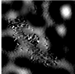


104 104 a b c d e f g h i j k l Figure 5.17: a, STM image (image parameters: V=94 mv, I=0.95 na, 7.5 nm x 7.5 nm) and b-l, vibrational maps of 94, 99, 104, 109, 114, 119, 124, 151, 166, 181, 196 mv.

105 105 From the vibrational mapping and length measurements, many of the amino acid residues can be determined. Figure 5.18 displays a sample of two proteins that have been partially sequenced using this technique. The amino acid residues that are not identified by an overlaid drawing are groups that cannot be identified by length, because of multiple amino acids have the same length, and did not show a distinguishable vibrational signature during mapping. a b Figure 5.18: a and b, Examples of amyloid peptide proteins that have been partially sequenced using length and vibrational data. Image parameters: a, V=265 mv, I=0.73 na, 12 nm x 12 nm. b, V=175 mv, I=1.0 na, 8 nm x 12 nm. 5.5 Summary and Discussion Evaporative deposition of the protein molecular wire was successful and single proteins were imaged on the Ag(111) surface. STM images taken of the protein reveal
106 106 individual amino acid residues. Partial sequencing of the protein was possible using only length measurements from the high resolution STM images. Vibrational spectroscopy and mapping shows a strong molecule-substrate vibration located on the backbone of the protein. The vibrational maps also identify other specific amino acid residues by comparison to Raman vibrational spectroscopy. The electronic properties of the protein molecular wire show a metallic behavior over the residues of the protein. A distinct trend is not seen when comparing the length of the residue to the resistance measurement. This implies the resistance of the residues are more influenced by their position in the protein rather than their length. Due to the random ordering of the residues this cannot be confirmed. The resistance of the backbone remains relatively constant as the length of the protein changes. This shows little conductance along the protein and more tunneling of the electrons through the backbone and into the sample below. The first images and study of a single protein using the STM are ground breaking achievements for the biological sciences. The knowledge that can be gained from single protein studies can impact many disciplines. This technique has the possibility to be applied to many other protein systems and can be used to map an entire protein sequence one protein at a time, giving direct verification of the protein sequence.
107 107 Chapter 6 Conclusions This dissertation has focused on the study of two systems, BETS 2 GaCl 4 and a nanoscale protein molecular wire. These systems have significance in charge transfer molecular electronics, molecular superconductivity and biological studies. The presented results show the richness of these systems and the ability of the STM to probe them. 6.1 Research Summary The study of the individual BETS and Et 4 N-GaCl 4 molecules and their combination on the surface has given insight into the charge transfer of these materials. The formation of the semi-ordered arrangement from previously disordered clusters clearly demonstrates the charge transfer process. Tunneling spectroscopy revealed the LUMO level of the Et 4 N-GaCl 4. At specific locations on the semi-ordered clusters, a superconducting gap in the tunneling spectroscopy was detected (Appendix D). The detection of the superconducting signal proves the charge transfer process is taking place in these clusters even though the exact molecular arrangement was not determined. The study of the λ-(bets) 2 GaCl 4 organic superconductor deposited on the Ag(111) surface gave very clear results. The structure of the sub-monolayer covered surface was determined by high resolution STM images and the packing mimicked the bulk crystal structure in a single active layer of double stacked BETS molecules. The superconducting gap was clearly seen in the tunneling spectroscopy and when fit with the phenomenological equation revealed a d xy paring symmetry. Study of the temperature
108 108 dependence of the superconducting gap recorded a clear transition from the superconducting to metal state at ~9 K. The influence of the molecular chain length on the superconducting gap width was also studied. As the length of the chain decreased below 50 molecular units, the width of the gap also decreased. The discoveries made during the study of this charge transfer system have made a large impact on the study of superconductivity in these systems [100,101]. The advances that have been made during this study open the door for the exploration of many other superconducting systems at the nanoscale. The successful deposition of the nanoscale protein molecular wire and the molecular resolution images of this protein mark the first STM study of an individual peptide sequence. The partial sequencing of the protein offers a novel routine for sequencing individual proteins with atomic resolution. Vibration signatures from the backbone and individual amino acid groups provide even more information about the protein and the molecule surface interaction. Spectroscopy taken on the backbone and individual amino acid groups show a metallic behavior independent of the residue or length of the protein. The nanoscale protein molecular wire and other protein based systems still need to be explored for their future use in molecular electronics. The first steps taken during this study will lay the ground work for the future study of many protein systems. The ability to study proteins individually is an achievement that could lead to many future breakthroughs in molecular electronics and biological sciences.
109 Future Research The ground breaking achievements that have resulted from this dissertation have far reaching consequences to other molecular and biomolecular systems. The future directions of research for these two systems have great promise for further discoveries. The study of similar charge transfer and protein systems can be pursued using these pioneering techniques. This study of the (BETS) 2 GaCl 4 molecular charge transfer superconducting system has proven that superconductivity exists at the nanoscale. This can impact the development of theoretical descriptions of how this unconventional superconductor mediates the Cooper pairs. In particular, the equation (Equation 7) used to fit the superconducting gap is only a phenomenological formula and is not derived from a theoretical background. Yet, as the study of these unconventional superconducting systems progress, better models may be employed. In turn, the STM studies such as this one can assist theory calculations for these materials, providing unique and accurate measurements to test new models. To illustrate how this ground breaking STM study can impact superconductivity research we can consider an alternate mediation scheme, in the absence of phonons, which is that of a spin-spin interaction that mediates the quasiparticle Cooper pairs [102]. The use of spin polarized STM could be a technique that would result in a better understanding of the spin order of these systems and result in proof of this type of mediation. Included in this Spin Polarized study would be the study of magnetic field induced superconductivity [66,103] which seems to be in conflict with traditional
110 110 superconductors where magnetic fields destroy superconductivity. A comprehensive study of this unique magnetic field induced effect could result in an understanding of unconventional superconductivity. Another interesting avenue to explore is the effect of other substrates on the formation of the superconducting molecular layer. The molecular layer that formed on the Ag(111) surface shows nearly identical crystal structure with the bulk crystal of λ- (BETS) 2 GaCl 4. The use of substrates with different lattice constants or a different surface orientation could apply in-plane pressure to the crystal layer. This pressure could manipulate the properties of the superconductor and may allow for further understanding of the superconductivity and possibly increase the T c. The study of the protein system opens the door for the study of many other biological systems. Understanding about the structure and function of biological systems is greatly needed. The technique demonstrated in this dissertation work can be applied to many other systems and can have a large impact in our understanding of these systems. A future study should include the full sequencing of a well-ordered and understood protein chain. The ability to directly sequence a protein is unique to this STM study and the adaptation of this technique to other systems could lead to a better understanding of the function of biological systems, such as those that use DNA/RNA for structural scaffolds in nano-engineering. It can be proposed that specific binding sites on individual amino acids could be imaged and probed using this technique. Biological systems have not been probed using the STM, this results in many systems that are ready to be studied.
111 111 The STM has proven itself over the years to be a very diverse tool for the study and manipulation of many different systems. I have shown that the extent of materials the STM can study continues to increase and there are a number of discoveries still to be made using the STM. The resolution, local probe capability and atomic manipulation of the STM will keep scientist busy for years to come with new challenges and discoveries.
112 112 References 1. G. Moore, Cramming More Components onto Integrated Circuits, Electronics 38, Number 8 (1965) 2. M. Lundstrom, Moore s Law Forever, Science 299, (2003) 3. A. Shakouri, S.-M. Kang, A. Bar-Cohen and B. Courtois, Scanning the Special Issue on On-Chip Thermal Engineering, Proceedings of the IEEE 94, (2006) 4. G. A. Prinz, Magnetoelectronics, Science 282, (1998) 5. C. Joachim, J. K. Gimzeqski and A. Aviram, Electronics Using Hybrid-Molecular and Mono-Molecular Devices, Nature 408, (2000) 6. Z. Tang, Nanoscale Phenomena. Basic Science to Device Applications. Spinger (2008) 7. M. Terrones, F, Banhart, N. Grobert, J.-C. Charlier, H. Terrones and P. M. Ajayan, Molecular Junctions by Joining Single Walled Carbon Nanotubes, Phys. Rev. Lett. 89, (2002) 8. E. Shapir, H. Cohen, A. Calzolari, C. Cavazzoni, D. A. Ryndyk, G. Cuniberti, A. Kotlyar, R. D. Felice and D. Porath, Electronic Structure of Single DNA Molecules resolved by Transverse Scanning Tunneling Spectroscopy, Nature Materials 7, (2008) 9. D. A. Ryndyk, Scanning Tunneling Spectroscopy of Single DNA Molecules, ACS Nano 7, (2009) 10. C. Lau and P. Wong, DoD Solid State Electronics Basic Research, www7.nationalacademies.org/bpa/sssc_mtgspring2004_lau
113 S. Datta lecture notes J. R. Schrieffer, Theory of superconductivity (W.A. Benjamin, New York, 1964) 13. I. A. Mastrangelo, High-Resolution Atomic Force Microscopy of Soluble Aβ42 Oligomers, J. Mol. Biol. 358, (2006) 14. A. P. Shivji, Scanning Tunnelling Microscopy Studies of β-amyloid Fibril Structure and Assembly, FEBS Letters 371, (1995) 15. D. Losic, High Resolution Scanning Tunnelling Microscopy of the β-amyloid Protein (Aβ1 40) of Alzheimer s Disease Suggests a Novel Mechanism of Oligomer Assembly, Journal of Structural Biology (2006) 16. G. Binnig, H. Rohrer, C. Gerber, and E. Weibel, Tunneling Through a Controllable Vacuum Gap, Appl. Phys. Lett. 40, 178 (1982) 17. G. Binnig, H. Rohrer, C. Gerber, and E. Weibel, 7X7 Reconstruction on Si(111) Resolved in Real Space, Phys. Rev. Lett. 50, 120 (1983) 18. J. Frenkel, On the Electrical Resistance of Contacts Between Solid Conductors, Phys. Rev. 36, 1604 (1930) 19. S.-W. Hla, Manipulating, Reacting and Constructing Single Molecules with a Scanning Tunneling Microscope Tip. Nanoscale Spectroscopy and its Application in Semiconductor Research, edited by Y. Watanabe, S. Heun, G. Salviati, N. Yamamoto, Lecture Notes in Physics, (Springer Verlag Heidelberg,) 222 (2002). 20. G. Dujardin, A. J. Mayne and F. Rose, Temperature Control of Electronic Channels through a Single Atom, Phys. Rev. Lett. 89, (2002)
114 L. J. Lauhon and W. Ho, Single-Molecule Chemistry and Vbrational Spectroscopy: Pyridine and Benzene on Cu(001), J. Phys. Chem. 104, 2463 (2000) 22. X. H. Qiu, G. V. Nazin and W. Ho, Vibronic States in Single Molecule Electron Transport, Phys. Rev. Lett. 92, (2004) 23. S. W. Hla, G. Meyer and K.-H. Rieder, Selective Bond Breaking of Single Iodobenzene Molecules with a Scanning Tunneling Microscope Tip, Chem. Phys. Lett. 370, 431 (2003) 24. J. G. Meyer, F. E. Olsson, and M. Persson, Controlling the Charge State of Individual Gold Adatoms, Science 305, 493 (2004) 25. J. A. Stroscio, and D. M. Eigler, Atomic and Molecular Manipulation with the Scanning Tunneling Microscope, Science 254, 1319 (1991) 26. S.-W. Hla, L. Bartels, G. Meyer, and K.-H. Rieder, Inducing all Steps of a Chemical Reaction with the Scanning Tunneling Microscope Tip: Towards Single Molecule Engineering, Phys. Rev. Lett. 85, 2777 (2000) 27. J. A. Heinrich, C. P. Lutz, J. A. Gupta and D. M. Eigler, Molecule Cascade, Science 298, 1381 (2002) 28. H. C. Manoharan, C. P. Lutz and D. M. Eigler, Quantum Mirages Formed by Coherent Projection of Electronic Structure, Nature 403, 512 (2000) 29. M. F. Crommie, C. P. Lutz and D. M. Eigler, Confinement of Electrons to Quantum Corrals on a Metal-Surface, Science 262, 218 (1993) 30. K.-F. Braun and S.-W. Hla, Probing the Conformation of Physisorbed Molecules at the Atomic-Scale using STM Manipulation, Nano Lett. 5, 73 (2005)
115 D. M. Eigler and E. K. Schweizer, Positioning Single Atoms with a Scanning Tunneling Microscope, Nature 344, 524 (1990) 32. L. Bartels, G. Meyer, and K.-H. Rieder, Basic Steps of Lateral Manipulation of Single Atoms and Diatomic Clusters with a Scanning Tunneling Microscope Tip, Phys. Rev. Lett. 79, 697 (1997) 33. S. W. Hla, K. F. Braun, and K.-H. Rieder, Detailed Atom Movement Mechanisms During a Quantum Corral Construction, Phys. Rev. B 67, R (2003) 34. A. Kühnle, G. Meyer, S. W. Hla, and K.-H. Rieder, Understanding Atom Movement During Lateral Manipulation with the STM Tip Using a Simple Simulation Method, Surf. Sci. 499, 15 (2002) 35. X. Bouju, C. Joachim, and C. Girard, Single-Atom Motion During a Lateral STM Manipulation, Phys. Rev. B 59, R7845 (1999) 36. C. R. Moon, L. S. Mattos, B. K. Foster, G. Zeltzer, and H. C. Manoharan, Quantum Holographic Encoding in a Two-Dimensional Electron Gas, Nature Nanotechnology 4, (2009) 37. F. J. Giessibl, High-Speed Force Sensor for Force Microscopy and Profilometry Utilizing a Quartz Tuning Fork, Appl. Phys. Lett. 73, 3956 (1998) 38. F. J. Giessibl, Atomic Resolution on Si(111)-(7 7) by Noncontact Atomic Force Microscopy with a Force Sensor Based on a Quartz Tuning Fork, Appl. Phys. Lett. 76, 1470 (2000) 39. C. J. Chen, Introduction to Scanning Tunneling Microscope Oxford University Press (1993)
116 R. A. Serway, Modern Physics 2 nd Ed. Saunders College Publishing, San Antonio (1997) 41. R. L. Liboff, Introductory Quantum Mechanics Addison Wesley, Boston (2003) 42. G. Binnig and H. Rohrer, Scanning Tunneling Microscopy From Birth to Adolescence, Rev. Mod. Phys. 59, (1987) 43. F. Jackel, U. G. E. Perera, V. Iancu, K.-F. Braun, N. Koch, J. P. Rabe and S.-W. Hla, Investigating Molecular Charge Transfer Complexes with a Low Temperature Scanning Tunneling Microscope, Phys. Rev. Lett. 100, (2008) 44. B. C. Stipe, M. A. Rezaei and W. Ho, Single-Molecule Vibrational Spectroscopy and Microscopy, Science 280, (1998) 45. W. Ho, Single-Molecule Chemistry, J of Chem. Phys. 117, (2002) 46. D. Acharya, K. Clark, A. Deshpande, J. Vaughn, K.-F. Braun and S.-W. Hla, Design and Construction of UHV-LT-STM System for Atom Manipulation for MBE Grown Semi-Conductor Surfaces, IEEE Nano 2006 Proceedings, (2006) 47. A. Deshpande, K. Clark, D. Acharya, J. Vaughn, K.-F. Braun and S.-W. Hla, Atomistic Construction by Using Scanning Tunneling Microscope Tip, IEEE Nano 2006 Proceedings, (2006) 48. K. Besocke, An Easily Operatable Scanning Tunneling Microscope, Surf. Sci. 181, 145 (1987) 49. G. Meyer, A Simple Low-Temperature Ultrahigh-Vacuum Scanning Tunneling Microscope Capable of Atomic Manipulation, Rev. Sci. Instrum. 67, 2960 (1996)
117 S.-W. Hla, K.-F. Braun, V. Iancu and A. Deshpande, Single Atom Extraction by Scanning Tunneling Microscope Tip-Crash and Nanoscale Surface Engineering, Nano Lett. 4, 1997 (2004) 51. J. Li, W-D, Schneider and R. Berndt, Local Density of States from Spectroscopic Scanning-Tunneling-Microscope Images: Ag(111), Phys. Rev. Lett. B, 56, (1997) 52. C. Kittel, Introduction to Solid State Physics. Wiley (1996) 53. W. Shockley, On the Surface States Associated with a Periodic Potential, Physical Review. 56, (1939) 54. R. S. Mulliken, Structures of Complexes Formed by Halogen Molecules with Aromatic and with Oxygenated Solvents, J. Am. Chem. Soc. 72, 600 (1950) 55. P. M. Allemand, K. C. Khemani, A. Koch, F. Wudl, K. Holczer, S. Donovan, G. Gruner and J. D. Thompson, Organic Molecular Soft Ferromagnetism in Fullerene C60, Science 253, (1991) 56. B. Narymbetov, A. Omerzu, V. V. Kabanov, J. Tokumoto, H. Kobayashi and D. Mihailovic, Origin of Ferromagnetic Exchange Interactions in a Fullerene- Organic Compound, Nature (London) 407, (2000) 57. N. Koch, S. Duhm, J. P. Rabe, A. Vollmer, and R. L. Johnson, Optimized Hole Injection with Strong Electron Acceptors at Organic-Metal Interfaces, Phys. Rev. Lett. 95, (2005)
118 F. Jackel, M. D. Watson, K. Mullen and R. P. Rabe, Prototypical Single-Molecule Chemical-Field-Effect Transistior with Nanometer-Sized Gates, Phys. Rev. Lett. 92, (2004) 59. W. A. Little, Possibility of Synthesizing an Organic Superconductor, Phys. Rev. 134, A1416-A1424 (1964) 60. L. B. Coleman, M. J. Cohen, D. J. Sandman, F. G. Yamagishi, A. F. Garito and A. J. Heeger, Superconducting Fluctuations and the Peierls Instability in an Organic Solid, Solid State Commun. 12, 1125 (1973) 61. J. Ferraris, D. O. Cowan, V. Walatka, Jr. and J. H. Perlstein, Electron Transfer in a New Highly Conducting Donor-Acceptor Complex, J. Am. Chem. Soc. 95, 948 (1973) 62. D. Jerome, A. Mazaud, M. Ribault and K. Bechgaard, Superconductivity in a Synthetic Organic (TMTSF) 2 PF 6, J. Physique Lett. 41, (1980) 63. E. Coronado, S. Curreli, C. Gimenez-Saiz and C. J. Gomez-Garcia, New Magnetic Conductors and Superconductors based on BEDT-TTF and BEDS-TTF, Synthetic Metals 154, (2005) 64. J. Yamada, R. Hayashi, H. Akutsu and S. Nakatsuji, New Organic Superconductors Based on Dihydro-TTF (DHTTF) Donors, Molecular Crystals and Liquid Crystals 440, (2005) 65. T. Shirahata, M. Kibune and T. Imakubo, New Ambient Pressure Organic Superconductors Kappa(H)- and Kappa(L)-(DMEDO- TSeF)(2)[Au(CN)(4)](THF), Chemical Communications 15, (2006)
119 M. Houzet, A. Buzdin, L. Bulaebskii and M. Maley, New Superconducting Phase in Field-Induced Organic Superconductor Lambda-(BETS)2FeCl4, Phys. Rev. Lett. 88, (2002) 67. A. E. Primenko, V. D. Kuznetsov, N. D. Kushch and E. B. Yakubskii, Magnetic Propeties of the New Organic Superconductor Lambda-(BETS)(2) GaCl4, J. of Exp. and Theor. Phys. 85, (1997) 68. K.-F. Braun and S.W. Hla, Charge Transfer in the TCNQ-sexithiophene Complex, J. of Chem. Phys. 129, (2008) 69. H. Kobayashi, A. Kobayashi and P. Cassoux, BETS as a Source of Molecular Magnetic Superconductors (BETS = bis(ethylenedithio)tetraselenafulvalene), Chem. Soc. Rev. 29, (2000) 70. C. W. Chu, J. M. E. Harper, T. H. Geballe and R. L. Greene, Pressure Dependence of the Metal-Insulator Transition in Tetrathiofulvalinium Tetracyanoquinodimethane (TTF-TCNW), Phys. Rev. Lett. 31, (1973) 71. H. Kobayashi, H. Cui and A. Kobayashi, Organic Metals and Superconductors Based on BETS (BETS = Bis(ethylenedithio)tetraselenafulvalene), Chem. Rev. 104, (2004) 72. R. Kato, H. Kobayashi, A. Kobayashi and Y Sasaki, Crystal Structure of(bmdt- TTF)3ClO4(1,2-Dichloroethane). Molecular Design for the Multi-Dimensional Molecular Conductor, Chem. Lett. 13, (1984)
120 H. Kobayashi, H. Tomita, T. Udaqawa, T. Naito and A. Kobayashi, New Organic Superconductor, λ-(bets) 2 GaCl 4 and Metal-Insulator Transition of BETS Conductor with Magnetic Anions (BETS = bis(ethlenedithio)tetraselenafulvalene), Synthetic Metals 70, (1995) 74. T. Courcet, I. Malfant, K. Pokhodnia and P. Cassoux, Bis(ethylenedithio)tetraselenafulvalene : Short-Cut Synthesis, X-ray Crystal Structure and p-electron Density Distribution, New J. Chem. 22, (1998) 75. J. P. Perdew, S. Burke, and M. Ernzerhof, Generalized Gradient Approximation Made Simple, Phys. Rev. Lett. 77, (1996) 76. H. K. Onnes, On the Sudden Rate at Which the Resistance of Mercury Disappears, Commun. Leiden, 120b, (1911) 77. J. Bardeen, L. N. Cooper and J. R. Schrieffer, Theory of Superconductivity, Phys. Rev. 108, (1957) 78. I. Giaever and K. Megerle, Study of Superconductors by Electron Tunneling, Phys. Rev. 122, (1961) 79. J. G. Bednorz and K. A. Muller, Possible High Tc Superconductivity in the Ba-La- Cu-) System, Z. Phys. B 64, (1986) 80. D. C. Mattis and M. Molina, Ratio 2Δ 0 /kt c in Superconductivity, Phys. Rev. B 44, (1991) 81. C. Enss and S. Hunklinger, Low Temperature Physics. Springer (2005) 82. D. J. Scalapino, The Case for d x 2 -y 2 Paring in the Cuprate Superconductors, Physics Reports 250, (1995)
121 K. Ichimura and K. Nomura, d-wave Pairing Symmetry in the Superconductivity of κ-(bedt-ttf) 2 X, J. Phys. Soc. Jpn. 75, (2006) 84. T. Arai, K. Ichimura, K. Nomura, S. Takasaki, J. Yamada, S. Nakatsuji and H. Anzai, Tunneling Spectroscopy on the Organic Superconductor k-bedt- TTF2Cu(NCS)2 Using STM, Phys. Rev. B 63, (2001) 85. J. Lee, J. A. Slezak and J. C. Davis, Spectroscopic Imaging STM Studies of High-Tc Superconductivity, J. of Phys. and Chem. of Solids. 66, (2005) 86. Y. Kohsaka, C. Taylor, P. Wahl, A. Schmidt, Jhinhwan Lee, K. Fujita, J. W. Alldredge, K. McElroy, Jinho Lee, H. Eisaki, S. Uchida, D.-H. Lee and J. C. Davis, How Cooper Pairs Vanish Approaching the Mott Insulator in Bi 2 Sr 2 CaCu 2 O 8+δ, Nature 454, (2008) 87. T. Kondo, R. Khazanov, T. Takauchi, J. Schmalian, and A. Kaminski, Competition Between the Pseudogap and Superconductivity in the High-Tc Copper Oxides, Nature 457, (2009) 88. K. Ichimura, M. Takami and K. Nomura, Direct Observation of d-wave Superconducting Gap in k-(bedt-ttf)2cu[n(cn)2]br with Scanning Tunneling Microscope, J. Phys. Soc. Jpn 77, (2008) 89. M. A. Tanatar, T. Ishiguro, H. Tanaka, A. Kobayashi and H. Kobayashi, Anisotropy of the Upper Critical Field of the Organic Suprconductor λ-(bets) 2 GaCl 4, J. Supercond. 12, (1999) 90.
122 M. P. Mattson, Pathways Towards and Away from Alzheimer s Disease, Nature 430, (2004) 92. Sigma-Aldrich Co. Data available at A. Schiffrin, A. Riemann, W. Auwarter, Y. Pennec, A. Weber-Bargioni, D. Cbetko, A. Cossaro, A. Morgante and J. V. Barth, Zwitterionic Self-Assembly of L- Methionine Nanogratings on Ag(111) Suface, PNAS 104, (2007) 94. J. Reichert, A. Schiffrin, W. Auwarter, A. Weber-Bargioni, M. Marschall, M. Dell Angela, D. Cvetko, G. Bavdek, A. Cossaro, A. Morgante and J. V. Barth, L-Tyrosine on Ag(111): Universality of the Amion Acid 2D Zwitterionic Bonding Scheme?, ACS NANO 4, (2010) 95. A. Schiffrin, J. Reichert, W. Auwarter, G. Jahnz, Y. Pennec, A. Weber-Bargioni, V. S. Stepanyuk, L. Niebergall, P. Bruno, and J. V. Barth, Self-Aligning Atomic Strings in Surface-Supported Biomolecular Gratings, Phys. Rev. B 78, (2008) 96. J. S. Suh and M. Moskovits, Surface-Enhanced Raman Spectroscopy of Amino Acids and Nucleotide Bases Adsorbed on Silver, J. Am. Chem. Soc. 108, (1986) 97. R. P. Rava and T. G. Spiro, Selective Enhancement of Tyrosine and Trytophan Resonance Raman Spectra via Ultraviolet Laser Excitation, J. Am. Chem. Soc. 106, (1984)
123 S. Stewart and P. M. Fredericks, Surface-Enhanced Raman Spectroscopy of Amino Acids Adsorbed on an Electrochemically Prepared Silver Surface, Spectrochimica Acta Part A 55, (1999) 99. S. A. Overman and G. J. Thomas, Raman Markers of Nonaromatic Side Chains in an a-helix Assembly: Ala, Asp, Glu, Gly, Ile, Leu, Lys, Ser, and Val Residues of Phae fd Subunits, Biochemistry 38, (1999) 100. K. Clark, A. Hassanien, S. Khan, K.-F. Braun, H. Tanaka and S.-W. Hla, Superconductivity in Just Four Pairs of (BETS) 2 GaCl 4 Molecules, Nature Nanotechnology 5, (2010) 101. J. Brooks, A Dash of Salt is Superconducting, Nature Nanotechnology 5, 244 (2010) 102. P. Monthoux, D. Pines and G. G. Lonzarich, Superconductivity Without Phonons, Nature 450, (2007) 103. S. Uji, H. Shinagawa, T. Terashima, T. Yakabe, Y. Terai, M. Tokumoto, A. Kobayashi, H. Tanaka and H. Kobayashi, Magnetic-Field-Induced Superconductivity in a Two-Dimensional Organic Conductor, Nature 410, (2001)
124 124 Appendix A: Publications and Presentations K. Clark, A. Hassanien, S. Khan, K.-F. Braun, H. Tanaka and S.-W. Hla, Superconductivity in Just Four Pairs of (BETS) 2 GaCl 4 Molecules, Nature Nanotechnology 5, (2010). D. Acharya, K. Clark, A. Deshpande, J. Vaughn, K.-F. Braun and S.-W. Hla, Design and Construction of UHV-LT-STM System for Atom Manipulation for MBE Grown Semi-Conductor Surfaces, IEEE Nano 2006 Proceedings, (2006). A. Deshpande, K. Clark, D. Acharya, J. Vaughn, K.-F. Braun and S.-W. Hla, Atomistic Construction by Using Scanning Tunneling Microscope Tip, IEEE Nano 2006 Proceedings, (2006). APS March Meeting 2010 March 2010 Oral Presentation: An Ultra-Thin Molecular Superconductor Made from Charge Transfer Complexes Poster Presentation: Magnetic Molecules on GaN: A Low Temperature STM Investigation AVS 56 th International Symposium and Exhibition November 2009 Oral Presentation: An Ultra-Thin Molecular Superconductor Oral Presentation: Magnetic Molecules on GaN Ohio University BNNT Mini-Conference May 2009 Oral Presentation: Magnetic Molecules on GaN Studied by LT-STM
125 125 DPG-Fruhjahrstagung, Dresden Germany March 2009 Oral Presentation: Magnetic Molecules on GaN Studied by LT-STM Poster Presentation: Novel Low Temperature Surface Reconstructions of GaN(000-1) NSS5 SPSTM2 Conference July 2008 Poster Presentation: GaN(000-1) Low Temperature Surface Reconstructions AVS Nanoelectronic Devices and Materials Symposium April 2007 Poster Presentation: Surface Reconstructions of GaN(000-1) at Low Temperatures Ohio Nanotechnology Summit April 2007 Poster Presentation: Low Temperature Surface Reconstructions of GaN(000-1)


126 126 Appendix B: Amino Acid Residue Properties The Ab 1-42 protein consists of 16 unique amino acid residues: Ala, Gly, Ser, His, Tyr, Val, Phe, Asp, Met Ile, Asn, Leu Glu, Gln, Lys, and Arg. Listed below is data on the residues including: chemical structure, molecular formula, molecular weight and vibrational spectroscopy curves courtesy of Sigma-Aldrich [92]. The energy scale for the vibrational curves are in both wavenumber (cm -1 ), shown in the upper value and mev the lower value. L-Aspartic Acid (Asp) Synonym (S)-(+)-Aminosuccinic acid (S)-Aminobutanedioic acid Molecular Formula HO 2 CCH 2 CH(NH 2 )CO 2 H Molecular Weight 133.1


127 127 L-Alanine (Ala) Synonym (S)-2-Aminopropionic acid L-α-Aminopropionic acid Molecular Formula C 3 H 7 NO 2 Molecular Weight 89.09
 Synonym")


128 128 L-Glutamic Acid (Glu) Synonym (S)-2-Aminopentanedioic acid Molecular Formula HO 2 CCH 2 CH 2 CH(NH 2 )CO 2 H Molecular Weight
-2-Amino-3-phenylpropionic acid")
CO 2 H Molecular Weight")
129 129 L-Phenylalanine (Phe) Synonym (S)-2-Amino-3-phenylpropionic acid Molecular Formula C 6 H 5 CH 2 CH(NH 2 )CO 2 H Molecular Weight


130 130 L-Arginine (Arg) Synonym (S)-2-Amino-5-guanidinopentanoic acid Molecular Formula H 2 NC(=NH)NH(CH 2 ) 3 CH(NH 2 )CO 2 H Molecular Weight


131 131 L-Histidine (His) Synonym (S)-2-Amino-3-(4-imidazolyl)propionic acid Molecular Formula C 6 H 9 N 3 O 2 Molecular Weight
-2-Amino-3-hydroxypropionic")
CO 2 H Molecular")
132 132 L-Serine (Ser) Synonym (S)-2-Amino-3-hydroxypropionic acid Molecular Formula HOCH 2 CH(NH 2 )CO 2 H Molecular Weight

133 133 Glycine (Gly) Synonym Aminoacetic acid Aminoethanoic acid Molecular Formula NH 2 CH 2 COOH Molecular Weight 75.07


134 134 L-Tyrosine (Tyr) Synonym (S)-2-Amino-3-(4-hydroxyphenyl)propionic acid 3-(4-Hydroxyphenyl)-L-alanine Molecular Formula 4-(HO)C 6 H 4 CH 2 CH(NH 2 )CO 2 H Molecular Weight
-α-Aminoisovaleric acid")
 2 CHCH(NH 2")
135 135 L-Valine (Val) Synonym (S)-α-Aminoisovaleric acid L-2-Amino-3-methylbutanoic acid Molecular Formula (CH 3 ) 2 CHCH(NH 2 )CO 2 H Molecular Weight


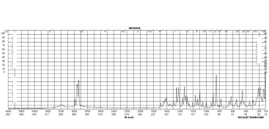
136 136 L-Glutamine (Gln) Synonym (S)-2,5-Diamino-5-oxopentanoic acid L-Glutamic acid 5-amide Molecular Formula H 2 NCOCH 2 CH 2 CH(NH 2 )CO 2 H Molecular Weight


 4 CH(NH 2 )CO 2")
137 137 L-Lysine (Lys) Synonym (S)-2,6-Diaminohexanoic acid monohydrochloride Molecular Formula H 2 N(CH 2 ) 4 CH(NH 2 )CO 2 H HCl Molecular Weight
-2-Amino-4-methylpentanoic acid")
CO 2 H Molecular Weight")
138 138 L-Leucine (Leu) Synonym (S)-2-Amino-4-methylpentanoic acid Molecular Formula (CH 3 ) 2 CHCH 2 CH(NH 2 )CO 2 H Molecular Weight
CO 2 H Molecular Weight")
139 139 L-Asparagine (Asn) Synonym (S)-2-Aminosuccinic acid 4-amide L-Aspartic acid 4-amide Molecular Formula H 2 NCOCH 2 CH(NH 2 )CO 2 H Molecular Weight


140 140 L-Isoleucine (Ile) Synonym (2S,3S)-2-Amino-3-methylpentanoic acid Molecular Formula C 2 H 5 CH(CH 3 )CH(NH 2 )CO 2 H Molecular Weight


141 141 L-Methionine (Met) Synonym (S)-2-Amino-4-(methylmercapto)butyric acid L-2-Amino-4-(methylthio)butanoic acid Molecular Formula CH 3 SCH 2 CH 2 CH(NH 2 )CO 2 H Molecular Weight
142 142 Appendix C: X-ray Diffraction of λ-(bets) 2 GaCl 4 X-ray diffraction measurements were performed at room temperature using a Rigaku AFC7R diffractometer. The X-ray diffraction pattern indicates a triclinic crystal structure. The unit cell is shown in Figure 3.5 with, a= (14) Å, b= (16) Å, c=6.5946(6) Å, α=96.736(2), β=98.370(2), γ= (2). Figure A1: X-ray diffraction data of λ-(bets) 2 GaCl 4 crystal.
143 143 Appendix D: Superconductivity in Semi-ordered BETS and Et 4 N-GaCl 4 Higher resolution spectroscopy around the Fermi energy shows a gap on selected regions of the amorphous structure (Figure A2). This gap is assigned as the superconducting gap of this charge transfer superconductor. The gap is only detectable at certain areas of the amorphous structure and indicates that this is an active area, an area where the charge transfer is taking place and the molecules are arranged in the proper order and in the correct ratio to produce superconductivity. Due to the amorphous structure of the BETS and Et 4 N-GaCl 4 clusters the exact assignment of the molecular structure resulting in the superconducting signal is difficult to determine. The 2:1 ratio of BETS to GaCl 4 must be met and orientation has to be similar to that of the bulk crystal, but exact determination is impossible due to the disorder of the cluster. The surprising result is the charge transfer ordering of the cluster still arranges in an ordered way to display superconductivity.

144 144 a b Figure A2: a, STM image of BETS and Et 4 N-GaCl 4 amorphous cluster. Oval drawn around single BETS molecule and the circle indicates the location of point spectroscopy. Image parameters: V=565 mv, I=1.5 na, 10 nm x 10 nm. b, Short range tunneling spectroscopy showing superconducting gap.
SUPPLEMENTARY INFORMATION
 Simultaneous and coordinated rotational switching of all molecular rotors in a network Y. Zhang, H. Kersell, R. Stefak, J. Echeverria, V. Iancu, U. G. E. Perera, Y. Li, A. Deshpande, K.-F. Braun, C. Joachim,
Scanning Tunneling Microscopy
 Scanning Tunneling Microscopy A scanning tunneling microscope (STM) is an instrument for imaging surfaces at the atomic level. Its development in 1981 earned its inventors, Gerd Binnig and Heinrich Rohrer
Scanning Tunneling Microscopy
 Scanning Tunneling Microscopy References: 1. G. Binnig, H. Rohrer, C. Gerber, and Weibel, Phys. Rev. Lett. 49, 57 (1982); and ibid 50, 120 (1983). 2. J. Chen, Introduction to Scanning Tunneling Microscopy,
3.1 Electron tunneling theory
 Scanning Tunneling Microscope (STM) was invented in the 80s by two physicists: G. Binnig and H. Rorher. They got the Nobel Prize a few years later. This invention paved the way for new possibilities in
REPORT ON SCANNING TUNNELING MICROSCOPE. Course ME-228 Materials and Structural Property Correlations Course Instructor Prof. M. S.
 REPORT ON SCANNING TUNNELING MICROSCOPE Course ME-228 Materials and Structural Property Correlations Course Instructor Prof. M. S. Bobji Submitted by Ankush Kumar Jaiswal (09371) Abhay Nandan (09301) Sunil
General concept and defining characteristics of AFM. Dina Kudasheva Advisor: Prof. Mary K. Cowman
 General concept and defining characteristics of AFM Dina Kudasheva Advisor: Prof. Mary K. Cowman Overview Introduction History of the SPM invention Technical Capabilities Principles of operation Examples
Scanning Tunneling Microscopy/Spectroscopy
 Scanning Tunneling Microscopy/Spectroscopy 0 Scanning Tunneling Microscope 1 Scanning Tunneling Microscope 2 Scanning Tunneling Microscope 3 Typical STM talk or paper... The differential conductance di/dv
tip of a current tip and the sample. Components: 3. Coarse sample-to-tip isolation system, and
 SCANNING TUNNELING MICROSCOPE Brief history: Heinrich Rohrer and Gerd K. Binnig, scientists at IBM's Zurich Research Laboratory in Switzerland, are awarded the 1986 Nobel Prize in physicss for their work
STM spectroscopy (STS)
") STM spectroscopy (STS) di dv 4 e ( E ev, r) ( E ) M S F T F Basic concepts of STS. With the feedback circuit open the variation of the tunneling current due to the application of a small oscillating voltage
STM spectroscopy (STS) di dv 4 e ( E ev, r) ( E ) M S F T F Basic concepts of STS. With the feedback circuit open the variation of the tunneling current due to the application of a small oscillating voltage
Chapter 10. Nanometrology. Oxford University Press All rights reserved.
 Chapter 10 Nanometrology Oxford University Press 2013. All rights reserved. 1 Introduction Nanometrology is the science of measurement at the nanoscale level. Figure illustrates where nanoscale stands
Scanning Tunneling Microscopy Studies of the Ge(111) Surface
 Surface") VC Scanning Tunneling Microscopy Studies of the Ge(111) Surface Anna Rosen University of California, Berkeley Advisor: Dr. Shirley Chiang University of California, Davis August 24, 2007 Abstract: This
VC Scanning Tunneling Microscopy Studies of the Ge(111) Surface Anna Rosen University of California, Berkeley Advisor: Dr. Shirley Chiang University of California, Davis August 24, 2007 Abstract: This
STM: Scanning Tunneling Microscope
 STM: Scanning Tunneling Microscope Basic idea STM working principle Schematic representation of the sample-tip tunnel barrier Assume tip and sample described by two infinite plate electrodes Φ t +Φ s =
Introduction to the Scanning Tunneling Microscope
 Introduction to the Scanning Tunneling Microscope A.C. Perrella M.J. Plisch Center for Nanoscale Systems Cornell University, Ithaca NY Measurement I. Theory of Operation The scanning tunneling microscope
Probing Molecular Electronics with Scanning Probe Microscopy
 Probing Molecular Electronics with Scanning Probe Microscopy Mark C. Hersam Assistant Professor Department of Materials Science and Engineering, Northwestern University, Evanston, IL 60208-3108 Ph: 847-491-2696,
= 6 (1/ nm) So what is probability of finding electron tunneled into a barrier 3 ev high?
 So what is probability of finding electron tunneled into a barrier 3 ev high?") STM STM With a scanning tunneling microscope, images of surfaces with atomic resolution can be readily obtained. An STM uses quantum tunneling of electrons to map the density of electrons on the surface
STM STM With a scanning tunneling microscope, images of surfaces with atomic resolution can be readily obtained. An STM uses quantum tunneling of electrons to map the density of electrons on the surface
Scanning Tunneling Microscopy
 Scanning Tunneling Microscopy References: 1. G. Binnig, H. Rohrer, C. Gerber, and Weibel, Phys. Rev. Lett. 49, 57 (1982); and ibid 50, 120 (1983). 2. J. Chen, Introduction to Scanning Tunneling Microscopy,
INTRODUCTION TO SCA\ \I\G TUNNELING MICROSCOPY
 INTRODUCTION TO SCA\ \I\G TUNNELING MICROSCOPY SECOND EDITION C. JULIAN CHEN Department of Applied Physics and Applied Mathematics, Columbia University, New York OXFORD UNIVERSITY PRESS Contents Preface
Lecture 4 Scanning Probe Microscopy (SPM)
") Lecture 4 Scanning Probe Microscopy (SPM) General components of SPM; Tip --- the probe; Cantilever --- the indicator of the tip; Tip-sample interaction --- the feedback system; Scanner --- piezoelectric
Lecture 4 Scanning Probe Microscopy (SPM) General components of SPM; Tip --- the probe; Cantilever --- the indicator of the tip; Tip-sample interaction --- the feedback system; Scanner --- piezoelectric
2) Atom manipulation. Xe / Ni(110) Model: Experiment:
 Atom manipulation. Xe / Ni(110) Model: Experiment:") 2) Atom manipulation D. Eigler & E. Schweizer, Nature 344, 524 (1990) Xe / Ni(110) Model: Experiment: G.Meyer, et al. Applied Physics A 68, 125 (1999) First the tip is approached close to the adsorbate
2) Atom manipulation D. Eigler & E. Schweizer, Nature 344, 524 (1990) Xe / Ni(110) Model: Experiment: G.Meyer, et al. Applied Physics A 68, 125 (1999) First the tip is approached close to the adsorbate
From nanophysics research labs to cell phones. Dr. András Halbritter Department of Physics associate professor
 From nanophysics research labs to cell phones Dr. András Halbritter Department of Physics associate professor Curriculum Vitae Birth: 1976. High-school graduation: 1994. Master degree: 1999. PhD: 2003.
Program Operacyjny Kapitał Ludzki SCANNING PROBE TECHNIQUES - INTRODUCTION
 Program Operacyjny Kapitał Ludzki SCANNING PROBE TECHNIQUES - INTRODUCTION Peter Liljeroth Department of Applied Physics, Aalto University School of Science peter.liljeroth@aalto.fi Projekt współfinansowany
Vacuum Pumps. Two general classes exist: Gas transfer physical removal of matter. Mechanical, diffusion, turbomolecular
 Vacuum Technology Vacuum Pumps Two general classes exist: Gas transfer physical removal of matter Mechanical, diffusion, turbomolecular Adsorption entrapment of matter Cryo, sublimation, ion Mechanical
Experimental methods in physics. Local probe microscopies I
 Experimental methods in physics Local probe microscopies I Scanning tunnelling microscopy (STM) Jean-Marc Bonard Academic year 09-10 1. Scanning Tunneling Microscopy 1.1. Introduction Image of surface
University of Massachusetts, Amherst
 PHYSICS 286: Modern Physics Laboratory SPRING 2010 (A. Dinsmore and K. Kumar) Feb 2009 Experiment 4: THE FRANCK HERTZ EXPERIMENT Electronic Excitations of a Gas, and Evidence for the Quantization of Atomic
Scanning Tunneling Microscopy
 Scanning Tunneling Microscopy References: 1. G. Binnig, H. Rohrer, C. Gerber, and Weibel, Phys. Rev. Lett. 49, 57 (1982); and ibid 50, 120 (1983). 2. J. Chen, Introduction to Scanning Tunneling Microscopy,
DEPOSITION OF THIN TiO 2 FILMS BY DC MAGNETRON SPUTTERING METHOD
 Chapter 4 DEPOSITION OF THIN TiO 2 FILMS BY DC MAGNETRON SPUTTERING METHOD 4.1 INTRODUCTION Sputter deposition process is another old technique being used in modern semiconductor industries. Sputtering
Techniken der Oberflächenphysik (Techniques of Surface Physics)
") Techniken der Oberflächenphysik (Techniques of Surface Physics) Prof. Yong Lei & Dr. Yang Xu Fachgebiet 3D-Nanostrukturierung, Institut für Physik Contact: yong.lei@tu-ilmenau.de yang.xu@tu-ilmenau.de
Techniken der Oberflächenphysik (Techniques of Surface Physics) Prof. Yong Lei & Dr. Yang Xu Fachgebiet 3D-Nanostrukturierung, Institut für Physik Contact: yong.lei@tu-ilmenau.de yang.xu@tu-ilmenau.de
Scanning Tunneling Microscopy. how does STM work? the quantum mechanical picture example of images how can we understand what we see?
 Scanning Tunneling Microscopy how does STM work? the quantum mechanical picture example of images how can we understand what we see? Observation of adatom diffusion with a field ion microscope Scanning
Scanning Tunneling Microscopy Transmission Electron Microscopy
 Scanning Tunneling Microscopy Transmission Electron Microscopy Speakers Burcu Başar Semih Gezgin Yavuz Selim Telis Place Hacettepe University Department of Chemical Engineering It s a small world after
Scanning tunneling microscopy
 IFM The Department of Physics, Chemistry and Biology Lab 72 in TFFM08 Scanning tunneling microscopy NAME PERS. - NUMBER DATE APPROVED Rev. Dec 2006 Ivy Razado Aug 2014 Tuomas Hänninen Contents 1 Introduction
Bonds and Wavefunctions. Module α-1: Visualizing Electron Wavefunctions Using Scanning Tunneling Microscopy Instructor: Silvija Gradečak
 3.014 Materials Laboratory December 8 th 13 th, 2006 Lab week 4 Bonds and Wavefunctions Module α-1: Visualizing Electron Wavefunctions Using Scanning Tunneling Microscopy Instructor: Silvija Gradečak OBJECTIVES
Introduction to Scanning Tunneling Microscopy
 Introduction to Scanning Tunneling Microscopy C. JULIAN CHEN IBM Research Division Thomas J. Watson Research Center Yorktown Heights, New York New York Oxford OXFORD UNIVERSITY PRESS 1993 CONTENTS List
672 Advanced Solid State Physics. Scanning Tunneling Microscopy
 672 Advanced Solid State Physics Scanning Tunneling Microscopy Biao Hu Outline: 1. Introduction to STM 2. STM principle & working modes 3. STM application & extension 4. STM in our group 1. Introduction
Nanotechnology Fabrication Methods.
 Nanotechnology Fabrication Methods. 10 / 05 / 2016 1 Summary: 1.Introduction to Nanotechnology:...3 2.Nanotechnology Fabrication Methods:...5 2.1.Top-down Methods:...7 2.2.Bottom-up Methods:...16 3.Conclusions:...19
Instrumentation and Operation
 Instrumentation and Operation 1 STM Instrumentation COMPONENTS sharp metal tip scanning system and control electronics feedback electronics (keeps tunneling current constant) image processing system data
Microscopy and Spectroscopy with Tunneling Electrons STM. Sfb Kolloquium 23rd October 2007
 Microscopy and Spectroscopy with Tunneling Electrons STM Sfb Kolloquium 23rd October 2007 The Tunnel effect T ( E) exp( S Φ E ) Barrier width s Barrier heigth Development: The Inventors 1981 Development:
Surface Studies by Scanning Tunneling Microscopy
 Surface Studies by Scanning Tunneling Microscopy G. Binnig, H. Rohrer, Ch. Gerber, and E. Weibel IBM Zurich Research Laboratory, 8803 Ruschlikon-ZH, Switzerland (Received by Phys. Rev. Lett. on 30th April,
Scanning Probe Microscopy (SPM)
") http://ww2.sljus.lu.se/staff/rainer/spm.htm Scanning Probe Microscopy (FYST42 / FAFN30) Scanning Probe Microscopy (SPM) overview & general principles March 23 th, 2018 Jan Knudsen, room K522, jan.knudsen@sljus.lu.se
http://ww2.sljus.lu.se/staff/rainer/spm.htm Scanning Probe Microscopy (FYST42 / FAFN30) Scanning Probe Microscopy (SPM) overview & general principles March 23 th, 2018 Jan Knudsen, room K522, jan.knudsen@sljus.lu.se
Introduction to Nanotechnology Chapter 5 Carbon Nanostructures Lecture 1
 Introduction to Nanotechnology Chapter 5 Carbon Nanostructures Lecture 1 ChiiDong Chen Institute of Physics, Academia Sinica chiidong@phys.sinica.edu.tw 02 27896766 Section 5.2.1 Nature of the Carbon Bond
Nanotechnology where size matters
 Nanotechnology where size matters J Emyr Macdonald Overview Ways of seeing very small things What is nanotechnology and why is it important? Building nanostructures What we can do with nanotechnology?
Investigating Nano-Space
 Name Partners Date Visual Quantum Mechanics The Next Generation Investigating Nano-Space Goal You will apply your knowledge of tunneling to understand the operation of the scanning tunneling microscope.
Spatially resolving density-dependent screening around a single charged atom in graphene
 Supplementary Information for Spatially resolving density-dependent screening around a single charged atom in graphene Dillon Wong, Fabiano Corsetti, Yang Wang, Victor W. Brar, Hsin-Zon Tsai, Qiong Wu,
Scanning Probe Microscopy. Amanda MacMillan, Emmy Gebremichael, & John Shamblin Chem 243: Instrumental Analysis Dr. Robert Corn March 10, 2010
 Scanning Probe Microscopy Amanda MacMillan, Emmy Gebremichael, & John Shamblin Chem 243: Instrumental Analysis Dr. Robert Corn March 10, 2010 Scanning Probe Microscopy High-Resolution Surface Analysis
Modern physics. 4. Barriers and wells. Lectures in Physics, summer
 Modern physics 4. Barriers and wells Lectures in Physics, summer 016 1 Outline 4.1. Particle motion in the presence of a potential barrier 4.. Wave functions in the presence of a potential barrier 4.3.
EXPERIMENT 9 Superconductivity & Ohm s Law
 Name: Date: Course number: MAKE SURE YOUR TA OR TI STAMPS EVERY PAGE BEFORE YOU START! Lab section: Partner's name(s): Grade: EXPERIMENT 9 Superconductivity & Ohm s Law 0. Pre-Laboratory Work [2 pts] 1.
Scanning Tunneling Microscopy. Wei-Bin Su, Institute of Physics, Academia Sinica
 Scanning Tunneling Microscopy Wei-Bin Su, Institute of Physics, Academia Sinica Tunneling effect Classical physics Field emission 1000 ~ 10000 V E V metal-vacuum-metal tunneling metal metal Quantum physics
Spectroscopies for Unoccupied States = Electrons
 Spectroscopies for Unoccupied States = Electrons Photoemission 1 Hole Inverse Photoemission 1 Electron Tunneling Spectroscopy 1 Electron/Hole Emission 1 Hole Absorption Will be discussed with core levels
Nanotechnology. Gavin Lawes Department of Physics and Astronomy
 Nanotechnology Gavin Lawes Department of Physics and Astronomy Earth-Moon distance 4x10 8 m (courtesy NASA) Length scales (Part I) Person 2m Magnetic nanoparticle 5x10⁻⁹ m 10 10 m 10 5 m 1 m 10-5 m 10-10
Spectroscopy at nanometer scale
 Spectroscopy at nanometer scale 1. Physics of the spectroscopies 2. Spectroscopies for the bulk materials 3. Experimental setups for the spectroscopies 4. Physics and Chemistry of nanomaterials Various
Vacuum Kelvin Force Probe Research Richard Williams August 1st 2008
 Vacuum Kelvin Force Probe Research Richard Williams August 1st 2008 Introduction Kelvin Force Probe Microscopy is an analytical method to measure the contact potential difference between a reference material
JARA FIT Ferienprakticum Nanoelektronik Experiment: Resonant tunneling in quantum structures
 JARA FIT Ferienprakticum Nanoelektronik 2013 Experiment: Resonant tunneling in quantum structures Dr. Mihail Ion Lepsa, Peter Grünberg Institut (PGI 9), Forschungszentrum Jülich GmbH 1. Introduction The
(Scanning Probe Microscopy)
") (Scanning Probe Microscopy) Ing-Shouh Hwang (ishwang@phys.sinica.edu.tw) Institute of Physics, Academia Sinica, Taipei, Taiwan References 1. G. Binnig, H. Rohrer, C. Gerber, and Weibel, Phys. Rev. Lett.
(Scanning Probe Microscopy) Ing-Shouh Hwang (ishwang@phys.sinica.edu.tw) Institute of Physics, Academia Sinica, Taipei, Taiwan References 1. G. Binnig, H. Rohrer, C. Gerber, and Weibel, Phys. Rev. Lett.
.Fritjaf Capra, The Tao of Physics
 Probing inside the atom and investigating its structure, science transcended the limits of our sensory imagination. From this point on, it could no longer rely with absolute certainty on logic and common
Final Reading Assignment: Travels to the Nanoworld: pages pages pages
 Final Reading Assignment: Travels to the Nanoworld: pages 152-164 pages 201-214 pages 219-227 Bottom-up nanofabrication Can we assemble nanomachines manually? What are the components (parts)? nanoparticles
Chapter 5 Nanomanipulation. Chapter 5 Nanomanipulation. 5.1: With a nanotube. Cutting a nanotube. Moving a nanotube
 Objective: learn about nano-manipulation techniques with a STM or an AFM. 5.1: With a nanotube Moving a nanotube Cutting a nanotube Images at large distance At small distance : push the NT Voltage pulse
Nanoelectronics. Topics
 Nanoelectronics Topics Moore s Law Inorganic nanoelectronic devices Resonant tunneling Quantum dots Single electron transistors Motivation for molecular electronics The review article Overview of Nanoelectronic
Application of single crystalline tungsten for fabrication of high resolution STM probes with controlled structure 1
 Application of single crystalline tungsten for fabrication of high resolution STM probes with controlled structure 1 A. N. Chaika a, S. S. Nazin a, V. N. Semenov a, V. G. Glebovskiy a, S. I. Bozhko a,b,
Surface atoms/molecules of a material act as an interface to its surrounding environment;
 1 Chapter 1 Thesis Overview Surface atoms/molecules of a material act as an interface to its surrounding environment; their properties are often complicated by external adsorbates/species on the surface
Surface Defects on Natural MoS 2
 Supporting Information: Surface Defects on Natural MoS 2 Rafik Addou 1*, Luigi Colombo 2, and Robert M. Wallace 1* 1 Department of Materials Science and Engineering, The University of Texas at Dallas,
Scanning Probe Microscopy
 1 Scanning Probe Microscopy Dr. Benjamin Dwir Laboratory of Physics of Nanostructures (LPN) Benjamin.dwir@epfl.ch PH.D3.344 Outline: Introduction: What is SPM, history STM AFM Image treatment Advanced
Imaging of Quantum Confinement and Electron Wave Interference
 : Forefront of Basic Research at NTT Imaging of Quantum Confinement and lectron Wave Interference Kyoichi Suzuki and Kiyoshi Kanisawa Abstract We investigated the spatial distribution of the local density
Quantum Condensed Matter Physics Lecture 12
 Quantum Condensed Matter Physics Lecture 12 David Ritchie QCMP Lent/Easter 2016 http://www.sp.phy.cam.ac.uk/drp2/home 12.1 QCMP Course Contents 1. Classical models for electrons in solids 2. Sommerfeld
MRSEC. Refrigerator Magnet Activity Guide. Quick Reference Activity Guide. a) b) c) = north = south. Activity Materials
 b) c) = north = south. Activity Materials") MRSEC Refrigerator Magnet Activity Guide Quick Reference Activity Guide Activity Materials Refrigerator magnet with removable probe strip Magnetic field diagrams Starting Points One of the great breakthroughs
MRSEC Refrigerator Magnet Activity Guide Quick Reference Activity Guide Activity Materials Refrigerator magnet with removable probe strip Magnetic field diagrams Starting Points One of the great breakthroughs
MSE 321 Structural Characterization
 Auger Spectroscopy Auger Electron Spectroscopy (AES) Scanning Auger Microscopy (SAM) Incident Electron Ejected Electron Auger Electron Initial State Intermediate State Final State Physical Electronics
Electron confinement in metallic nanostructures
 Electron confinement in metallic nanostructures Pierre Mallet LEPES-CNRS associated with Joseph Fourier University Grenoble (France) Co-workers : Jean-Yves Veuillen, Stéphane Pons http://lepes.polycnrs-gre.fr/
MSN551 LITHOGRAPHY II
 MSN551 Introduction to Micro and Nano Fabrication LITHOGRAPHY II E-Beam, Focused Ion Beam and Soft Lithography Why need electron beam lithography? Smaller features are required By electronics industry:
Microscopy Cryostat System
 OF AMERICA, INC. Microscopy Cryostat System RC102-CFM Microscopy Cryostat offers fast cooldown, high efficiency, lowest thermal drift, excellent temperature stability and ultra low vibration Optical cryostat
NANOSCIENCE: TECHNOLOGY AND ADVANCED MATERIALS
 UNIVERSITY OF SOUTHAMPTON PHYS6014W1 SEMESTER 2 EXAMINATIONS 2012-2013 NANOSCIENCE: TECHNOLOGY AND ADVANCED MATERIALS DURATION 120 MINS (2 Hours) This paper contains 8 questions Answer ALL questions in
Spectroscopy of Nanostructures. Angle-resolved Photoemission (ARPES, UPS)
") Spectroscopy of Nanostructures Angle-resolved Photoemission (ARPES, UPS) Measures all quantum numbers of an electron in a solid. E, k x,y, z, point group, spin E kin, ϑ,ϕ, hν, polarization, spin Electron
Spectroscopy of Nanostructures Angle-resolved Photoemission (ARPES, UPS) Measures all quantum numbers of an electron in a solid. E, k x,y, z, point group, spin E kin, ϑ,ϕ, hν, polarization, spin Electron
CHAPTER 11 Semiconductor Theory and Devices
 CHAPTER 11 Semiconductor Theory and Devices 11.1 Band Theory of Solids 11.2 Semiconductor Theory 11.3 Semiconductor Devices 11.4 Nanotechnology It is evident that many years of research by a great many
Nanomaterials and their Optical Applications
 Nanomaterials and their Optical Applications Winter Semester 2013 Lecture 02 rachel.grange@uni-jena.de http://www.iap.uni-jena.de/multiphoton Lecture 2: outline 2 Introduction to Nanophotonics Theoretical
Surfaces, Interfaces, and Layered Devices
 Surfaces, Interfaces, and Layered Devices Building blocks for nanodevices! W. Pauli: God made solids, but surfaces were the work of Devil. Surfaces and Interfaces 1 Interface between a crystal and vacuum
CITY UNIVERSITY OF HONG KONG. Theoretical Study of Electronic and Electrical Properties of Silicon Nanowires
 CITY UNIVERSITY OF HONG KONG Ë Theoretical Study of Electronic and Electrical Properties of Silicon Nanowires u Ä öä ªqk u{ Submitted to Department of Physics and Materials Science gkö y in Partial Fulfillment
Citation for published version (APA): Mendoza, S. M. (2007). Exploiting molecular machines on surfaces s.n.
: Mendoza, S. M. (2007). Exploiting molecular machines on surfaces s.n.") University of Groningen Exploiting molecular machines on surfaces Mendoza, Sandra M IMPORTANT NOTE: You are advised to consult the publisher's version (publisher's PDF) if you wish to cite from it. Please
University of Groningen Exploiting molecular machines on surfaces Mendoza, Sandra M IMPORTANT NOTE: You are advised to consult the publisher's version (publisher's PDF) if you wish to cite from it. Please
Gaetano L Episcopo. Scanning Electron Microscopy Focus Ion Beam and. Pulsed Plasma Deposition
 Gaetano L Episcopo Scanning Electron Microscopy Focus Ion Beam and Pulsed Plasma Deposition Hystorical background Scientific discoveries 1897: J. Thomson discovers the electron. 1924: L. de Broglie propose
Contents. What is AFM? History Basic principles and devices Operating modes Application areas Advantages and disadvantages
 Contents What is AFM? History Basic principles and devices Operating modes Application areas Advantages and disadvantages Figure1: 2004 Seth Copen Goldstein What is AFM? A type of Scanning Probe Microscopy
CHARACTERIZATION of NANOMATERIALS KHP
 CHARACTERIZATION of NANOMATERIALS Overview of the most common nanocharacterization techniques MAIN CHARACTERIZATION TECHNIQUES: 1.Transmission Electron Microscope (TEM) 2. Scanning Electron Microscope
SOLID STATE PHYSICS PHY F341. Dr. Manjuladevi.V Associate Professor Department of Physics BITS Pilani
 SOLID STATE PHYSICS PHY F341 Dr. Manjuladevi.V Associate Professor Department of Physics BITS Pilani 333031 manjula@bits-pilani.ac.in Characterization techniques SEM AFM STM BAM Outline What can we use
PHYS 3313 Section 001 Lecture #21 Monday, Nov. 26, 2012
 PHYS 3313 Section 001 Lecture #21 Monday, Nov. 26, 2012 Superconductivity Theory, The Cooper Pair Application of Superconductivity Semi-Conductor Nano-technology Graphene 1 Announcements Your presentations
Nanoscale work function measurements by Scanning Tunneling Spectroscopy
 Related Topics Tunneling effect, Defects, Scanning Tunneling Microscopy (STM), (STS), Local Density of States (LDOS), Work function, Surface activation, Catalysis Principle Scanning tunneling microscopy
Introduction to Nanotechnology Chapter 5 Carbon Nanostructures Lecture 1
 Introduction to Nanotechnology Chapter 5 Carbon Nanostructures Lecture 1 ChiiDong Chen Institute of Physics, Academia Sinica chiidong@phys.sinica.edu.tw 02 27896766 Carbon contains 6 electrons: (1s) 2,
single-electron electron tunneling (SET)
") single-electron electron tunneling (SET) classical dots (SET islands): level spacing is NOT important; only the charging energy (=classical effect, many electrons on the island) quantum dots: : level spacing
single-electron electron tunneling (SET) classical dots (SET islands): level spacing is NOT important; only the charging energy (=classical effect, many electrons on the island) quantum dots: : level spacing
Photoemission Spectroscopy
 FY13 Experimental Physics - Auger Electron Spectroscopy Photoemission Spectroscopy Supervisor: Per Morgen SDU, Institute of Physics Campusvej 55 DK - 5250 Odense S Ulrik Robenhagen,
Lesson 4: Tools of the Nanosciences. Student Materials
 Lesson 4: Tools of the Nanosciences Student Materials Contents Black Box Lab Activity: Student Instructions and Worksheet Seeing and Building Small Things: Student Reading Seeing and Building Small Things:
Spectroscopy at nanometer scale
 Spectroscopy at nanometer scale 1. Physics of the spectroscopies 2. Spectroscopies for the bulk materials 3. Experimental setups for the spectroscopies 4. Physics and Chemistry of nanomaterials Various
Nanostructure. Materials Growth Characterization Fabrication. More see Waser, chapter 2
 Nanostructure Materials Growth Characterization Fabrication More see Waser, chapter 2 Materials growth - deposition deposition gas solid Physical Vapor Deposition Chemical Vapor Deposition Physical Vapor
Water clustering on nanostructured iron oxide films
 ARTICLE Received 12 May 2013 Accepted 22 May 2014 Published 30 Jun 2014 Water clustering on nanostructured iron oxide films Lindsay R. Merte1,2, Ralf Bechstein1, W. Guowen Peng3, Felix Rieboldt1, Carrie
Resistivity vs. Temperature of a Superconductor WARNING
 Resistivity vs. Temperature of a Superconductor 1.0 Expected Learning Outcomes Calibrate a transducer (silicon diode) for low-temperature measurements and measure temperatures down to that of boiling liquid
Studying Metal to Insulator Transitions in Solids using Synchrotron Radiation-based Spectroscopies.
 PY482 Lecture. February 28 th, 2013 Studying Metal to Insulator Transitions in Solids using Synchrotron Radiation-based Spectroscopies. Kevin E. Smith Department of Physics Department of Chemistry Division
Experiment Ma8: Superconductivity
 Experiment Ma8: Superconductivity 1 Overview Superconductivity is a phenomenon occurring at low temperatures. H.K. Onnes observed in year 1911 that the electrical resistivity of some metals sank abruptly
Practical 1P4 Energy Levels and Band Gaps
 Practical 1P4 Energy Levels and Band Gaps What you should learn from this practical Science This practical illustrates some of the points from the lecture course on Elementary Quantum Mechanics and Bonding
Barrier Penetration, Radioactivity, and the Scanning Tunneling Microscope
 Physics 5K Lecture Friday April 20, 2012 Barrier Penetration, Radioactivity, and the Scanning Tunneling Microscope Joel Primack Physics Department UCSC Topics to be covered in Physics 5K include the following:
Practical 1P4 Energy Levels and Band Gaps
 Practical 1P4 Energy Levels and Band Gaps What you should learn from this practical Science This practical illustrates some of the points from the lecture course on Elementary Quantum Mechanics and Bonding
Solid Surfaces, Interfaces and Thin Films
 Hans Lüth Solid Surfaces, Interfaces and Thin Films Fifth Edition With 427 Figures.2e Springer Contents 1 Surface and Interface Physics: Its Definition and Importance... 1 Panel I: Ultrahigh Vacuum (UHV)
CH676 Physical Chemistry: Principles and Applications. CH676 Physical Chemistry: Principles and Applications
 CH676 Physical Chemistry: Principles and Applications History of Nanotechnology: Time Line Democritus in ancient Greece: concept of atom 1900 : Rutherford : discovery of atomic nucleus The first TEM was
Chapter 29 Molecular and Solid-State Physics
 Chapter 29 Molecular and Solid-State Physics GOALS When you have mastered the content of this chapter, you will be able to achieve the following goals: Definitions Define each of the following terms, and
Nanoscale characteristics by Scanning Tunneling Spectroscopy
 Related Topics Tunneling effect, Scanning Tunneling Microscopy (STM), (STS), Local Density of States (LDOS), Band structure, Band Gap, k-space, Brioullin Zone, Metal, Semi-Metal, Semiconductor Principle
Kavli Workshop for Journalists. June 13th, CNF Cleanroom Activities
 Kavli Workshop for Journalists June 13th, 2007 CNF Cleanroom Activities Seeing nm-sized Objects with an SEM Lab experience: Scanning Electron Microscopy Equipment: Zeiss Supra 55VP Scanning electron microscopes
Advanced Lab Course. X-Ray Photoelectron Spectroscopy 1 INTRODUCTION 1 2 BASICS 1 3 EXPERIMENT Qualitative analysis Chemical Shifts 7
 Advanced Lab Course X-Ray Photoelectron Spectroscopy M210 As of: 2015-04-01 Aim: Chemical analysis of surfaces. Content 1 INTRODUCTION 1 2 BASICS 1 3 EXPERIMENT 3 3.1 Qualitative analysis 6 3.2 Chemical
and another with a peak frequency ω 2
 Physics Qualifying Examination Part I 7-Minute Questions September 13, 2014 1. A sealed container is divided into two volumes by a moveable piston. There are N A molecules on one side and N B molecules