Introduction to Graphene Physics
|
|
|
- Francine Davis
- 6 years ago
- Views:
Transcription
1 XIX VIETNAM SCHOOL OF PHYSICS (VSOP-19) Quy Nhon, August 3-18, 013 Introduction to Graphene Physics Gilles Montambaux Day 1 courses 1-1


2 Gilles Montambaux, Laboratoire de Physique des Solides, Orsay, France Saclay Palaiseau Orsay users.lps.u-psud.fr/montambaux


3 Graphene is... D crystal massless relativistic Fermions monolayer electrostatic doping nanoribbons bilayers 3

4 Graphene : from discovery to Nobel prize.. Graphene, the world s first -dimensional fabric Posted Oct 6, 004, 3:30 PM ET Researchers at The University of Manchester and Chernogolovka, Russia have created the first-ever single-atom-thick substance, a fabric they call graphene. The substance is stable, flexible, and highly conductive, and researchers believe it could be used to create computers made from a single molecule. Professor Andre Geim at The University of Manchester was able to extract a single plane of graphite crystal, resulting in the new fabric. The hope is that the fabric will be used in the future to create nanotubes, transistors for microscopic computers, that could result in some seriously small electronic gadgetry. The Nobel Prize in Physics 010 was awarded jointly to Andre Geim and Konstantin Novoselov "for groundbreaking experiments regarding the two-dimensional material graphene" 4
5 Number of papers on ArXiv with the key word «graphene» Total : about 6000 papers in 011!!! 5
 Graphene and")

6 Science, 34, 530 (009) Graphene and other D crystals BN, NbSe, BiSr CaCu Ox (005)

7 7
8 A few references Electric field effect in atomically thin carbon films,. K. Novoselov, A. Geim et al., Science 306, 666 (004) Two-dimensional gas of massless Dirac fermions in graphene, K. Novoselov, A. Geim et al., Nature 438, 197 (005) Experimental observation on the quantum Hall effect and Berry s phase in graphene, Y. Zhang, Y. Tan, H. Stormer and P. Kim, Nature 438, 01 (005) The rise of graphene, A. Geim and K. Novoselov, Nat. Mat. 6, 183 (007) The electronic properties of graphene, A.H. Castro Neto, F. Guinea, N.M.R. Peres, K.S. Novoselov and A.K. Geim, Rev. Mod. Phys. 81, 109 (009) Graphene: Status and prospects, A. Geim, Science, 34, 530 (009) Electronic transport in two dimensional graphene S. Das Sarma, S. Adams, A. Hwang and E. Rossi, Rev. Mod. Phys. (011) Epitaxial graphene electronic structure and transport W. A. de Heer, C. Berger et al., J. Phys. D: Appl. Phys. 43, (010), arxiv: See also ttp:// ( a list of review papers) also wikipedia
9 Tentative outline History, fabrication, first experiments Electronic structure, wave functions, DOS, new Landau levels Dirac spectrum Linearized Hamiltonian Berry Phase Absence of backscattering Klein tunnelling Classical transport Ribbons, edge states Magnetic field effect Landau levels, wave functions, QHE Edge states Bilayers Quantum transport, weak-antilocalization Graphene physics in other systems Engineering of Dirac points 9


10 Carbon 3d 1d 0d d Graphite Graphene Fullerene 1985 sp Nanotube Diamond Multi-wall 1991 Single-wall 1993 sp 3 10

11 graphene, fullerenes, nanotubes and graphite sp 11
 and conduction bands (CB) meet in points (K,K ) in reciprocal space [Dirac points].")
12 Why is graphene interesting? Graphene = D honeycomb lattice Direct space atoms per unit cell Peculiar band structure: -The valence (VB) and conduction bands (CB) meet in points (K,K ) in reciprocal space [Dirac points]. -The dispersion relation close to the Dirac points is linear : electrons are massless! Energy spectrum CB -The VB is full, the CB is empty: the Fermi level is right at the Dirac points. 1Bz K K Graphene is a valleys (K,K'), D gapless semiconductor. Electrons are massless and chiral. VB 1
 1789 Named from greek grajein (A.")
 1960-1980 Graphite")
![intercalation compounds 1985 Fullerenes [Kroto, Curl, Smalley]](/docs-images/72/67469742/images/13-2.jpg "1991-1993 Carbon nanotubes [Iijima] 199-1993 few layers graphite")
13 Short history 1564 Discovery of graphite (plumbago) 1779 Graphite is carbon (C. Scheele) 1789 Named from greek grajein (A. Werner) Graphite: pencils, light bulbs, neutrons moderator, HOPG (graphite monocrystal) Graphite intercalation compounds 1985 Fullerenes [Kroto, Curl, Smalley] Carbon nanotubes [Iijima] few layers graphite on metal substrate 13

![] 005 Graphene quantum Hall effect [N.,G.](/docs-images/72/67469742/images/14-1.jpg ",Zhang,Stormer,Kim, Columbia] 006 Graphene bilayer QHE [N.,G.")
14 Modern history 004 Exfoliated contacted (and gated) graphene on amorphous SiO substrate [Novoselov, Geim, Manchester] 004 Epitaxial graphene on SiC [Berger, de Heer, Georgia Tech.] 005 Graphene quantum Hall effect [N.,G.,Zhang,Stormer,Kim, Columbia] 006 Graphene bilayer QHE [N.,G.,McCann, Falko] 008 CVD fabrication 011 : over 6000 published papers since QHE

![Hofstadter butterfly [Rammal] P.](/docs-images/72/67469742/images/15-1.jpg "Wallace ε 1984-1988 Connection to +1 field theory")

15 History: theory 1947 Graphene band structure [Wallace] 1956 Graphene Landau levels [McClure] 1985 Hofstadter butterfly [Rammal] P. Wallace ε Connection to +1 field theory [Semenoff, DiVincenzo & Mele, Fradkin, Haldane, etc.] ~90 s Theory of carbon nanotubes [Dresselhauss, Saito, Ando, Guinea, etc. 15 Φ/Φ 0
16 Experimental techniques a) Mechanically exfoliated graphene (the scotch trick) Take a (monocrystallite) graphite pencil. Draw on a Si/SiO substrate: you will deposit graphite flakes. A small fraction are monolayers. Detect them with an optical microscope (300nm SiO thickness). Contact the monolayer with metallic leads (gold) contacts (Au) graphene (~1 to 100 μm ) n-si 300nm of SiO Geim,Novoselov et al. (Manchester) P. Kim et al. (Columbia)


17 The Scotch trick Novoselov et al. (Manchester) 004 P. Kim et al. (Columbia) 005 SiO substrate

18 The Scotch trick tools: optical microscope, AFM, SEM, Raman, QHE 18


19 Difficult to locate..! Substrate SiO : 1 cm² graphene sheet: 1 mm² --- (100 mm)² 1 m² (100) m² Paris: 10 km² One graphene monolayer is enough to modify the optical contrast 300nm of SiO If not for this simple yet effective way to scan substrates in search of graphene crystallites, they would probably remain undiscovered today (Geim, Novoselov) 19
20 Contact the monolayer with metallic leads (gold e.g.) Field effect : A gate voltage V g controls the density of electrons in the graphene sheet ( electrostatic doping ) Capacitor = graphene / insulator SiO /conductor n-si contacts (Au) Nc CgVg / e e n C 4e c 0 g Nc A e A / d a V g a 7.10 cm. V 10 1 n-si d 300nm SiO Novoselov et al., Science 004
21 (1/k) Electric Field Effect in Graphene conductivity Hall effect 3 1 T =10K V g (V) σ=n c (V g )eμ 1/ρ xy =ne/b B =T T =10K holes electrons V g (V) /r xy (1/k) Novoselov, Geim et al. Science (005) simple behaviour: practically constant μ, σ(n c 0) 0 1
 Thermal decomposition of SiC at high temperature (~1400 o C) - high vacuum (0001)")

22 b) Epitaxial graphene on SiC Epitaxial growth of graphene layers on top of a SiC monocristal A.Charrier et al., J. Applied Physics 9, 479 (00) Thermal decomposition of SiC at high temperature (~1400 o C) - high vacuum (0001) Si-face Si C Si Si SiC (0001) C-face Graphene on SiC Berger et al., J. Phys. Chem. 004 By controling temperature, growth of 1 to ~100 graphene layers C. Berger, W. De Heer et al. (Atlanta) Graphene layers behave as if they were isolated.
23 3
24 4
25 5
26 6
27 7


28 c) CVD : chemical vapor decomposition ~1000 K Ni Bae et al., Nature Nanotechnology 5, 574 (010) Massive production Yu et al., APL 93, (008) 8

29 9
 X.Du et al.")

 Shivaraman,")
30 d) Suspended graphene Bolotin et al., Columbia, SSC (008) X.Du et al., Rutgers (009) m cm /. V s terminals FQHE Bolotin et al., Columbia, Nature (009) Du et al., Rutgers, Nature (009) Shivaraman, et al. Nanoletters (009)
31 e) Graphene on Boron Nitride 31

32 Graphene electronic structure Graphene = D honeycomb carbon crystal Carbon: 6 electrons 1s, s p hybridation: 1 orbital s and orbitals p 3 orbitals sp -3 coplanar σ bonds, angle 10 : honeycomb structure covalent bonding 1 orbital p z perpendicular to the plane 1 conduction e per C Half-filled band cf: benzène
33 «Honeycomb lattice» is not a Bravais lattice a=1.4 A a1 a t t t=.8ev a a a t =-0.eV a = C-C distance a 0 = lattice parameter Triangular Bravais lattice + atoms per unit cell
34 «Honeycomb lattice» is not a Bravais lattice a=1.4 A a1 a t t t=.8ev a a a t =-0.eV a = C-C distance a 0 = lattice parameter Triangular Bravais lattice + atoms per unit cell
35 Real Space Reciprocal space a 1 * a K * a 1 a a 1 3 K G M K Triangular Bravais lattice + identical atoms per unit cell a 0.14nm 1 * * K ( a1 a ) G 3 3a * 4 a i GK KK ' 4 3 3a
36 Nearest neighbor tight-binding model for the conduction electrons, Wallace 1947 Nearest neighbor hopping t 1 conduction electron per atom (next nearest hopping t ) j H t j j h. c j, j' A j' B t j j ' j j ' ' ja ja jb jb h. j, j ' c g1 t t + Bloch theorem... 36
37 Electronic spectrum Hopping between nearest neighbors ik R + Bloch theorem ( r R) e ( r ) 1 ik Rj j j e ca( k ) ja cb( k ) j B N cells a1 a H ik a e ika ec k t e e c k 1 B( ) (1 ) A( ) ika ika ec k t e e c k 1 A( ) (1 ) B( ) B A t t H k ca( k ) ca( k ) e cb( k) cb( k) with H k f A B * 0 f( k) ( k) 0 ika ika f k t e e 1 ( ) (1 )
38 x Hamiltonian H k f * 0 f( k) ( k) 0 ika ika f k t e e 1 ( ) (1 ) e ( k ) f ( k ) e( k ) 0? * * a a 1 Ka 1 3 K K Ka 3 1 * * K ( a1 a ) G 3 38
 ika ika f k t e e 1 ( ) (1 ) t t E( k ) f ( k ) t '[cos k. a cos k. a cos k.( a a )] 1 1 t t.8 ev ' 0.")
39 Next nearest neighbors a1 a gk ( ) f ( k ) ca( k ) ca( k ) E * f ( k ) g( k ) cb( k ) cb( k ) E( k ) f ( k ) gk ( ) ika ika f k t e e 1 ( ) (1 ) t t E( k ) f ( k ) t '[cos k. a cos k. a cos k.( a a )] 1 1 t t.8 ev ' 0. ev
 e i k ae ik.")
40 Wave functions H k f 0 f( k) ( k) 0 * H k i k 0 e e ( k) i k e 0 k ( r ) e i k ae ik. r 1 k arg[ f( k)] a band index 40


41 Topological properties k ( r ) e ik. r 1 a i e k u e k ik. r k 1 B i u u. d k =. d k k k k k k C «Berry phase» C Berry phase effects on electronic properties, D. Xiao, M.C. Chang, Q. Niu, arxiv: Consequences on Landau levels spectrum Roth Wilkinson ( g ) / en n B a d g B 1
42 Topological properties k ( r ) e i k ae ik. r 1 No backscattering Diffusion from k to k : Fermi golden rule k k' i 1 k ' ( ) kk ' 1 i kk ' cos k P V e V e P( ) 0 4
43 Expansion near the Dirac points ika ika f k t e e 1 ( ) (1 ) H f ( K q) c( q iq ) K K H K K 0 qx iqy c qx iqy 0 p q A mc c( px ipy) c( px ipy) mc x y B K K Dirac eq. for a relativistic particle in D c v F 3 ta 10 m.s 6-1 H c p mc K z e( p) p c m c 4 e( q) vf q 43
44 How to write the effective linearized Hamiltonian 0 qx iqy H KK, ' c c( qxx qyy ) qx iqy 0 A B A B 0 qx iqy 0 0 qx iqy H c qx iqy 0 0 qx iqy 0 or A B B A 0 qx iqy 0 0 qx iqy H c c q. z qx iq y 0 0 qx iqy 0 4 x 4 effective Hamiltonian Two uncoupled valleys HK c p * H c p K HK c p H c p K 44
45 How to write the effective linearized Hamiltonian H KK, ' A B 0 qx iqy c qx iqy 0 q arctan q q y x H 0 cq e i q e i 0 q 1 e ( q) ac q k 1 1 ik. r iq. r ik '. r iq. r ( r ) e e i q iq ae ae The wave function is a linear combination of the contributions of the two valleys
46 Density of states 1953 e a ( px py) e cp re ( ) gg s v e v F Thermodynamics, transport g s = g v = p e m spin degeneracy valley degeneracy k e F n v n F F c c Remember : for e k a in d dimensions r( e) e d / a 1 46
47 Landau levels graphene gg s v re ( ) e c Onsager semi-classical quantization rule eb N( el) ( n g) g h re ( ) gs m DEG N( e) e d / a el c ( n g) e B g 0 e L c n B el n B a / [( g) ] d e L eb ( n g) m 1 e L ( n ) m g B 1
 vf q q a sin 3 q q arctan q q y x K K")
48 Beyond linearization «Trigonal warping» e 3t 8 ( q) vf q q a sin 3 q q arctan q q y x K K 48

 i i K K Bostwick et al. Nat.")
49 ARPES experiments : Angular Resolved Photemission Spectroscopy measure the dispersion relation hn e e k k k f f i i e ( k ) i i K K Bostwick et al. Nat. Phys. 007
50 Cyclotron mass m * A e e e( k ) Novoselov, Geim et al., Nature 005 graphene m * e v F F e v n F F c m * v F n c 50

")

51 Boron Nitride : Dirac equation with a mass Blue and red atoms are now different : B and N site energies different H k f * ( k) f( k) Ek f ( k ) t.8 ev 5.9eV C-C B-N mdc qx iqy H c c q. mdc z qx iqy mdc
 FQHE Random")

52 Graphene on Boron Nitride substrate P. Kim group, Nature Nanotechnology (010) FQHE Random crystallographic orientation to the substrate t.8 ev 50meV Giovannetti, et al. PRB (007) BN is a perfectly clean substrate 5
53 GaAs mobility, Pfeiffer et al. Suspended graphene (008) Graphene on h-bn (010) Graphene on SiO (004) 53
54 Transport 54
55 (1/k) Conductivity e v n F F c 3 n c a V g e ( ) F e kl F e h 1 T =10K V g (V) n c av g l ( e )??? e F ( T)??? 55
56 Physics of the neutrality point Thermally activated carriers kt B ne( T) nh( T) 7 ta E F =0 Specific heat 8 (3) kbt C( T) kb ta Conductivity e le e ( F 0, T) 4ln kbt h v F f ( T) ( e ) de e e e ( F, T 0) h k l F e 56
57 e le e ( F 0, T) 4ln kbt h v T classical plasma 400K F e v n F F c n c =av g T F (n c ) e e ( F, T 0) k l h degenerate gas F e n cm c T T F degenerate gas T T F classical plasma T T F degenerate gas 57
58 (1/k) Conductivity 3 σ=n(v g )eμ e n c v av n F F c g e ( ) F e kl F e h 1 T =10K V g (V) l ( e )??? e F Very small temperature dependence le Cte ( e ) e V F F g l e l e 1 k F e ( ) Cte kf ( e F) e F Vg F neutral impurities charged screened impurities Nomura, MacDonald, PRL 007 should depend on dielectric constant see also M.Monteverde et al. PRL (010) resonant impurities
59 Suspended graphene Bolotin et al., Columbia PRL 101, (008) e k F l e k F ( ) h 4 e k F L h diffusive ballistic 59

 n c Explication : «flaques» de trous")
60 (1/k) conductivity minimum Should vanish at the neutrality point? 3 1 T =10K V g (V) Tan et al. PRL 99, (007) n c Explication : «flaques» de trous et d électrons 0 c 60 n 0 Yacoby et al., Nature Phys. 008
61 GaAs mobility, Pfeiffer et al. Suspended graphene (008) Graphene on h-bn (010) Graphene on SiO (004) 61
62 Strong dependence on the nature of substrate, impurities «Graphenes» Fabrication Substrate exfoliated SiC CVD SiO SiC Suspended BN 6
63 Disorder A B H K 0 px ipy ( r) 1 0 c V ( r) m( r) c * px ipy ( r) Scalar Static distorsions («ripples») Local A-B dissymetry Intervalley (K, K ) coupling and range of the disorder potential long range disorder does not couple valleys short range disorder couples valleys 63
64 Klein tunneling 64

")
65 Klein tunneling effect Oskar Klein ( ) 65
66 1 ) Potential step ) Potential barrier 66
67 E p x m E c p x V 0 Evanescent wave Transmission E p c m c 4 x Transmission V0 mc E Evanescent wave Transmission V mc E V mc 0 0 mc E V mc 0 67
68 E p x m E c p x 4 E pxc m c E c p p Evanescent mode x y Transmission V E mc 0 0 y V E cp 68
69 E p c m c 4 x E V mc 0 E Transmission 69
70 E p c m c 4 x E V mc 0 E Transmission 70
71 E p c m c 4 x E V mc 0 E Transmission 71
72 E p c m c 4 x V mc E V mc 0 0 E Evanescent wave 7
73 E p c m c 4 x V mc E V mc 0 0 E Evanescent wave 73
74 E p c m c 4 x V mc E V mc 0 0 E Evanescent wave 74
75 E p c m c 4 x V mc E V mc 0 0 E Evanescent wave 75
76 E p c m c 4 x V mc E V mc 0 0 E Evanescent wave 76
77 E p c m c 4 x E V E mc 0 77
78 E p c m c 4 x E V E mc 0 Transmission 78
79 E p x m E c p x 4 E pxc m c E c p p x y Evanescent mode Transmission E V mc 0 E V0 cpy 79
80 E c p p x y Transmission if : cp V E y 0 sin V 0 E E Perfect transmission if 0 Transmission( 0 ) depends on E V 0 80
81 Velocity E c p x E a vf k v 1 k E a v k F k Wave function k ( r ) e i k ae ik. r 1 81
sin t + Continuity")
82 Potential step coscost T ( ) t sin E V E sin ( 0 )sin t + Continuity equations

83 Potential step T() coscost T ( ) t sin Esin ( V0 E)sin t E/V 0 =0 E/V 0 =0.5 Evanesce nt waves E/V 0 =0.5 E/V 0= 0.75 E/V 0 T=0 E/V 0 =1 V sin transmission 0 E E When E approches V 0, more and more evanescent modes
84 Potential step T() E V 0 0 E V coscost T ( ) t sin Esin ( V0 E)sin t coscost T ( ) t cos Esin ( E V0 )sin t 84

85 Potential barrier + Continuity equations 85
86 J.N. Fuchs et P. Allain, Klein Tunneling in graphene : optics with massless electrons EPJB, arxiv:

 E sin ( V E)sin q ( V E)cos x 0 0 t t T( )")
87 Potential barrier T() E/V 0 =0.4, l=l/(hv F /V 0 )=4.85 E/V 0 =0.9, l=6.91 Katsnelson, Novoselov and Geim, Nat. Phys., 60 (006) E sin ( V E)sin q ( V E)cos x 0 0 t t T( ) cos cos cos cos cos sin (1 sin sin ) t qxl t qxl t 87
88 A very interesting case : E V 0 E V c q k 0 x y 0 q x i k y E c k k x y T( ) cosh cos klsin y 88
 k y cosh kl y n W Tworzydlo et al.")
89 Propagation through ballistic graphene at the neutrality point E ' E V q k 0 0 x y E V 0 normal contacts 1 T( 0) k y cosh kl y n W Tworzydlo et al., PRL 96, 4680 (006) 89

90 T n G 1 L cosh n W e 4 Tn h n Called «pseudo-diffusive regime, because the distribution of the transmission coefficients is the same as in a diffusive disordered system W L G 4 e W h L min min 4 e h W / L Miao et al., Science, 317, 1530 (007) 90
Electronic properties of graphene. Jean-Noël Fuchs Laboratoire de Physique des Solides Université Paris-Sud (Orsay)
") Electronic properties of graphene Jean-Noël Fuchs Laboratoire de Physique des Solides Université Paris-Sud (Orsay) Cargèse, September 2012 3 one-hour lectures in 2 x 1,5h on electronic properties of graphene
Electronic properties of graphene Jean-Noël Fuchs Laboratoire de Physique des Solides Université Paris-Sud (Orsay) Cargèse, September 2012 3 one-hour lectures in 2 x 1,5h on electronic properties of graphene
Graphite, graphene and relativistic electrons
 Graphite, graphene and relativistic electrons Introduction Physics of E. graphene Y. Andrei Experiments Rutgers University Transport electric field effect Quantum Hall Effect chiral fermions STM Dirac
A BIT OF MATERIALS SCIENCE THEN PHYSICS
 GRAPHENE AND OTHER D ATOMIC CRYSTALS Andre Geim with many thanks to K. Novoselov, S. Morozov, D. Jiang, F. Schedin, I. Grigorieva, J. Meyer, M. Katsnelson A BIT OF MATERIALS SCIENCE THEN PHYSICS CARBON
Carbon based Nanoscale Electronics
 Carbon based Nanoscale Electronics 09 02 200802 2008 ME class Outline driving force for the carbon nanomaterial electronic properties of fullerene exploration of electronic carbon nanotube gold rush of
Graphene: massless electrons in flatland.
 Graphene: massless electrons in flatland. Enrico Rossi Work supported by: University of Chile. Oct. 24th 2008 Collaorators CMTC, University of Maryland Sankar Das Sarma Shaffique Adam Euyuong Hwang Roman
Graphene and Quantum Hall (2+1)D Physics
D Physics") The 4 th QMMRC-IPCMS Winter School 8 Feb 2011, ECC, Seoul, Korea Outline 2 Graphene and Quantum Hall (2+1)D Physics Lecture 1. Electronic structures of graphene and bilayer graphene Lecture 2. Electrons
The 4 th QMMRC-IPCMS Winter School 8 Feb 2011, ECC, Seoul, Korea Outline 2 Graphene and Quantum Hall (2+1)D Physics Lecture 1. Electronic structures of graphene and bilayer graphene Lecture 2. Electrons
Graphene. Tianyu Ye November 30th, 2011
 Graphene Tianyu Ye November 30th, 2011 Outline What is graphene? How to make graphene? (Exfoliation, Epitaxial, CVD) Is it graphene? (Identification methods) Transport properties; Other properties; Applications;
Graphene: fundamentals
 Graphene: fundamentals François Peeters Condensed Matter Theory group Department of Physics University of Antwerp Email: francois.peeters@uantwerpen.be https://www.uantwerpen.be/en/rg/cmt/ Chemistry Graphitic
Graphene - most two-dimensional system imaginable
 Graphene - most two-dimensional system imaginable A suspended sheet of pure graphene a plane layer of C atoms bonded together in a honeycomb lattice is the most two-dimensional system imaginable. A.J.
Manipulation of Dirac cones in artificial graphenes
 Manipulation of Dirac cones in artificial graphenes Gilles Montambaux Laboratoire de Physique des Solides, Orsay CNRS, Université Paris-Sud, France - Berry phase Berry phase K K -p Graphene electronic
Overview. Carbon in all its forms. Background & Discovery Fabrication. Important properties. Summary & References. Overview of current research
 Graphene Prepared for Solid State Physics II Pr Dagotto Spring 2009 Laurene Tetard 03/23/09 Overview Carbon in all its forms Background & Discovery Fabrication Important properties Overview of current
Graphene and Carbon Nanotubes
 Graphene and Carbon Nanotubes 1 atom thick films of graphite atomic chicken wire Novoselov et al - Science 306, 666 (004) 100μm Geim s group at Manchester Novoselov et al - Nature 438, 197 (005) Kim-Stormer
3-month progress Report
 3-month progress Report Graphene Devices and Circuits Supervisor Dr. P.A Childs Table of Content Abstract... 1 1. Introduction... 1 1.1 Graphene gold rush... 1 1.2 Properties of graphene... 3 1.3 Semiconductor
Graphene and Planar Dirac Equation
 Graphene and Planar Dirac Equation Marina de la Torre Mayado 2016 Marina de la Torre Mayado Graphene and Planar Dirac Equation June 2016 1 / 48 Outline 1 Introduction 2 The Dirac Model Tight-binding model
Lectures Graphene and
 Lectures 15-16 Graphene and carbon nanotubes Graphene is atomically thin crystal of carbon which is stronger than steel but flexible, is transparent for light, and conducts electricity (gapless semiconductor).
Electronic properties of Graphene and 2-D materials
 Electronic properties of Graphene and 2-D materials 2D materials background Carbon allotropes Graphene Structure and Band structure Electronic properties Electrons in a magnetic field Onsager relation
Scanning tunneling microscopy and spectroscopy of graphene layers on graphite
 Scanning tunneling microscopy and spectroscopy of graphene layers on graphite Adina Luican, Guohong Li and Eva Y. Andrei Department of Physics and Astronomy, Rutgers University, Piscataway, New Jersey
ELECTRONIC ENERGY DISPERSION AND STRUCTURAL PROPERTIES ON GRAPHENE AND CARBON NANOTUBES
 ELECTRONIC ENERGY DISPERSION AND STRUCTURAL PROPERTIES ON GRAPHENE AND CARBON NANOTUBES D. RACOLTA, C. ANDRONACHE, D. TODORAN, R. TODORAN Technical University of Cluj Napoca, North University Center of
Bloch, Landau, and Dirac: Hofstadter s Butterfly in Graphene. Philip Kim. Physics Department, Columbia University
 Bloch, Landau, and Dirac: Hofstadter s Butterfly in Graphene Philip Kim Physics Department, Columbia University Acknowledgment Prof. Cory Dean (now at CUNY) Lei Wang Patrick Maher Fereshte Ghahari Carlos
Theories of graphene. Reinhold Egger Heinrich-Heine-Universität Düsseldorf Kolloquium, Hamburg
 Theories of graphene Reinhold Egger Heinrich-Heine-Universität Düsseldorf Kolloquium, Hamburg 1. 5. 011 Graphene monolayer Mother of all-carbon materials (fullerenes, nanotubes, graphite): made of benzene
TRANSVERSE SPIN TRANSPORT IN GRAPHENE
 International Journal of Modern Physics B Vol. 23, Nos. 12 & 13 (2009) 2641 2646 World Scientific Publishing Company TRANSVERSE SPIN TRANSPORT IN GRAPHENE TARIQ M. G. MOHIUDDIN, A. A. ZHUKOV, D. C. ELIAS,
2-D Layered Materials 1
 2-D Layered Materials 1 Flatlands beyond Graphene Why the interest? 2D crystal with extraordinarily few defects Exotic electrical behaviors E = v F P (massless Dirac fermions) Efficient tunneling through
Physics of graphene. Hideo Aoki Univ Tokyo, Japan. Yasuhiro Hatsugai Univ Tokyo / Tsukuba, Japan Takahiro Fukui Ibaraki Univ, Japan
 Physics of graphene Hideo Aoki Univ Tokyo, Japan Yasuhiro Hatsugai Univ Tokyo / Tsukuba, Japan Takahiro Fukui Ibaraki Univ, Japan Purpose Graphene a atomically clean monolayer system with unusual ( massless
Graphene films on silicon carbide (SiC) wafers supplied by Nitride Crystals, Inc.
 wafers supplied by Nitride Crystals, Inc.") 9702 Gayton Road, Suite 320, Richmond, VA 23238, USA Phone: +1 (804) 709-6696 info@nitride-crystals.com www.nitride-crystals.com Graphene films on silicon carbide (SiC) wafers supplied by Nitride Crystals,
9702 Gayton Road, Suite 320, Richmond, VA 23238, USA Phone: +1 (804) 709-6696 info@nitride-crystals.com www.nitride-crystals.com Graphene films on silicon carbide (SiC) wafers supplied by Nitride Crystals,
Initial Stages of Growth of Organic Semiconductors on Graphene
 Initial Stages of Growth of Organic Semiconductors on Graphene Presented by: Manisha Chhikara Supervisor: Prof. Dr. Gvido Bratina University of Nova Gorica Outline Introduction to Graphene Fabrication
Spin orbit interaction in graphene monolayers & carbon nanotubes
 Spin orbit interaction in graphene monolayers & carbon nanotubes Reinhold Egger Institut für Theoretische Physik, Düsseldorf Alessandro De Martino Andreas Schulz, Artur Hütten MPI Dresden, 25.10.2011 Overview
The many forms of carbon
 The many forms of carbon Carbon is not only the basis of life, it also provides an enormous variety of structures for nanotechnology. This versatility is connected to the ability of carbon to form two
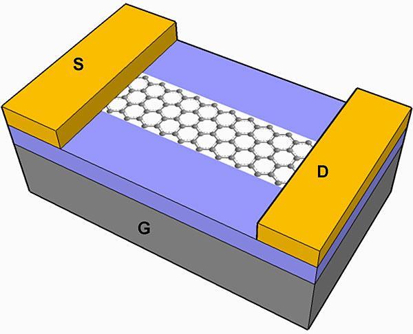
Graphene transistor. Seminar I a. Mentor: doc. dr. Tomaž Rejec. April Abstract
 Graphene transistor Seminar I a Jan Srpčič Mentor: doc. dr. Tomaž Rejec April 2015 Abstract The topic of this seminar is graphene and its possible applications in the field of electronics, most notably
From graphene to Z2 topological insulator
 From graphene to Z2 topological insulator single Dirac topological AL mass U U valley WL ordinary mass or ripples WL U WL AL AL U AL WL Rashba Ken-Ichiro Imura Condensed-Matter Theory / Tohoku Univ. Dirac
GRAPHENE the first 2D crystal lattice
 GRAPHENE the first 2D crystal lattice dimensionality of carbon diamond, graphite GRAPHENE realized in 2004 (Novoselov, Science 306, 2004) carbon nanotubes fullerenes, buckyballs what s so special about
arxiv: v1 [cond-mat.mes-hall] 26 Sep 2013
![arxiv: v1 [cond-mat.mes-hall] 26 Sep 2013](/thumbs/83/88173709.jpg "arxiv: v1 [cond-mat.mes-hall] 26 Sep 2013") Berry phase and the unconventional quantum Hall effect in graphene Jiamin Xue Microelectronic Research Center, The University arxiv:1309.6714v1 [cond-mat.mes-hall] 26 Sep 2013 of Texas at Austin, Austin,
Berry phase and the unconventional quantum Hall effect in graphene Jiamin Xue Microelectronic Research Center, The University arxiv:1309.6714v1 [cond-mat.mes-hall] 26 Sep 2013 of Texas at Austin, Austin,
Graphene A One-Atom-Thick Material for Microwave Devices
 ROMANIAN JOURNAL OF INFORMATION SCIENCE AND TECHNOLOGY Volume 11, Number 1, 2008, 29 35 Graphene A One-Atom-Thick Material for Microwave Devices D. DRAGOMAN 1, M. DRAGOMAN 2, A. A. MÜLLER3 1 University
Quantum Oscillations in Graphene in the Presence of Disorder
 WDS'9 Proceedings of Contributed Papers, Part III, 97, 9. ISBN 978-8-778-- MATFYZPRESS Quantum Oscillations in Graphene in the Presence of Disorder D. Iablonskyi Taras Shevchenko National University of
& Dirac Fermion confinement Zahra Khatibi
 Graphene & Dirac Fermion confinement Zahra Khatibi 1 Outline: What is so special about Graphene? applications What is Graphene? Structure Transport properties Dirac fermions confinement Necessity External
Topological Phases under Strong Magnetic Fields
 Topological Phases under Strong Magnetic Fields Mark O. Goerbig ITAP, Turunç, July 2013 Historical Introduction What is the common point between graphene, quantum Hall effects and topological insulators?...
Graphene electronics
 Graphene electronics Alberto Morpurgo Main collaborators J. Oostinga, H. Heersche, P. Jarillo Herrero, S. Russo, M. Craciun, L. Vandersypen, S. Tarucha, R. Danneau, P. Hakkonen A simple tight-binding H
Graphene. L. Tetard 1,2. (Dated: April 7, 2009) 1 Oak Ridge National Laboratory, Oak Ridge, TN USA
 1 Oak Ridge National Laboratory, Oak Ridge, TN USA") Graphene L. Tetard 1,2 1 Oak Ridge National Laboratory, Oak Ridge, TN 37831-6123 USA 2 Department of Physics, University of Tennessee, Knoxville, TN 37996, USA (Dated: April 7, 2009) 1 Diamond, graphite,
Graphene L. Tetard 1,2 1 Oak Ridge National Laboratory, Oak Ridge, TN 37831-6123 USA 2 Department of Physics, University of Tennessee, Knoxville, TN 37996, USA (Dated: April 7, 2009) 1 Diamond, graphite,
Transport properties through double-magnetic-barrier structures in graphene
 Chin. Phys. B Vol. 20, No. 7 (20) 077305 Transport properties through double-magnetic-barrier structures in graphene Wang Su-Xin( ) a)b), Li Zhi-Wen( ) a)b), Liu Jian-Jun( ) c), and Li Yu-Xian( ) c) a)
Effects of Interactions in Suspended Graphene
 Effects of Interactions in Suspended Graphene Ben Feldman, Andrei Levin, Amir Yacoby, Harvard University Broken and unbroken symmetries in the lowest LL: spin and valley symmetries. FQHE Discussions with
Physics of Nanotubes, Graphite and Graphene Mildred Dresselhaus
 Quantum Transport and Dynamics in Nanostructures The 4 th Windsor Summer School on Condensed Matter Theory 6-18 August 2007, Great Park Windsor (UK) Physics of Nanotubes, Graphite and Graphene Mildred
Theory of Quantum Transport in Graphene and Nanotubes II
 CARGESE7B.OHP (August 26, 27) Theory of Quantum Transport in Graphene and Nanotubes II 1. Introduction Weyl s equation for neutrino 2. Berry s phase and topological anomaly Absence of backscattering in
Electron Interactions and Nanotube Fluorescence Spectroscopy C.L. Kane & E.J. Mele
 Electron Interactions and Nanotube Fluorescence Spectroscopy C.L. Kane & E.J. Mele Large radius theory of optical transitions in semiconducting nanotubes derived from low energy theory of graphene Phys.
Spring College on Computational Nanoscience May Electric Transport in Carbon Nanotubes and Graphene
 145-8 Spring College on Computational Nanoscience 17-8 May 1 Electric Transport in Carbon Nanotubes and Graphene Philip KIM Dept. of Physics, Columbia University New York U.S.A. Electric Transport in Nanotubes
Part 1. March 5, 2014 Quantum Hadron Physics Laboratory, RIKEN, Wako, Japan 2
 MAR 5, 2014 Part 1 March 5, 2014 Quantum Hadron Physics Laboratory, RIKEN, Wako, Japan 2 ! Examples of relativistic matter Electrons, protons, quarks inside compact stars (white dwarfs, neutron, hybrid
Graphene Novel Material for Nanoelectronics
 Graphene Novel Material for Nanoelectronics Shintaro Sato Naoki Harada Daiyu Kondo Mari Ohfuchi (Manuscript received May 12, 2009) Graphene is a flat monolayer of carbon atoms with a two-dimensional honeycomb
STM and graphene. W. W. Larry Pai ( 白偉武 ) Center for condensed matter sciences, National Taiwan University NTHU, 2013/05/23
 Center for condensed matter sciences, National Taiwan University NTHU, 2013/05/23") STM and graphene W. W. Larry Pai ( 白偉武 ) Center for condensed matter sciences, National Taiwan University NTHU, 2013/05/23 Why graphene is important: It is a new form of material (two dimensional, single
STM and graphene W. W. Larry Pai ( 白偉武 ) Center for condensed matter sciences, National Taiwan University NTHU, 2013/05/23 Why graphene is important: It is a new form of material (two dimensional, single
Infrared magneto-spectroscopy of graphene-based systems
 Infrared magneto-spectroscopy of graphene-based systems M. Orlita, C. Faugeras, G. Martinez P. Neugebauer, M. Potemski Laboratoire National des Champs Magnétiques Intenses CNRS, Grenoble, France Collaborators:
Graphene The Search For Two Dimensions. Christopher Scott Friedline Arizona State University
 Graphene The Search For Two Dimensions Christopher Scott Friedline Arizona State University What Is Graphene? Single atomic layer of graphite arranged in a honeycomb crystal lattice Consists of sp 2 -bonded
Hartmut Buhmann. Physikalisches Institut, EP3 Universität Würzburg Germany
 Hartmut Buhmann Physikalisches Institut, EP3 Universität Würzburg Germany Part I and II Insulators and Topological Insulators HgTe crystal structure Part III quantum wells Two-Dimensional TI Quantum Spin
Supplementary Figure 2 Photoluminescence in 1L- (black line) and 7L-MoS 2 (red line) of the Figure 1B with illuminated wavelength of 543 nm.
 and 7L-MoS 2 (red line) of the Figure 1B with illuminated wavelength of 543 nm.") PL (normalized) Intensity (arb. u.) 1 1 8 7L-MoS 1L-MoS 6 4 37 38 39 4 41 4 Raman shift (cm -1 ) Supplementary Figure 1 Raman spectra of the Figure 1B at the 1L-MoS area (black line) and 7L-MoS area (red
PL (normalized) Intensity (arb. u.) 1 1 8 7L-MoS 1L-MoS 6 4 37 38 39 4 41 4 Raman shift (cm -1 ) Supplementary Figure 1 Raman spectra of the Figure 1B at the 1L-MoS area (black line) and 7L-MoS area (red
Nanoscience quantum transport
 Nanoscience quantum transport Janine Splettstößer Applied Quantum Physics, MC2, Chalmers University of Technology Chalmers, November 2 10 Plan/Outline 4 Lectures (1) Introduction to quantum transport (2)
1. Nanotechnology & nanomaterials -- Functional nanomaterials enabled by nanotechnologies.
 Novel Nano-Engineered Semiconductors for Possible Photon Sources and Detectors NAI-CHANG YEH Department of Physics, California Institute of Technology 1. Nanotechnology & nanomaterials -- Functional nanomaterials
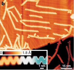
Supplementary Figure S1. AFM images of GraNRs grown with standard growth process. Each of these pictures show GraNRs prepared independently,
 Supplementary Figure S1. AFM images of GraNRs grown with standard growth process. Each of these pictures show GraNRs prepared independently, suggesting that the results is reproducible. Supplementary Figure
SiC Graphene Suitable For Quantum Hall Resistance Metrology.
 SiC Graphene Suitable For Quantum Hall Resistance Metrology. Samuel Lara-Avila 1, Alexei Kalaboukhov 1, Sara Paolillo, Mikael Syväjärvi 3, Rositza Yakimova 3, Vladimir Fal'ko 4, Alexander Tzalenchuk 5,
Electronic Properties of Hydrogenated Quasi-Free-Standing Graphene
 GCOE Symposium Tohoku University 2011 Electronic Properties of Hydrogenated Quasi-Free-Standing Graphene Danny Haberer Leibniz Institute for Solid State and Materials Research Dresden Co-workers Supervising
Gate-induced insulating state in bilayer graphene devices
 Gate-induced insulating state in bilayer graphene devices Jeroen B. Oostinga, Hubert B. Heersche, Xinglan Liu, Alberto F. Morpurgo and Lieven M. K. Vandersypen Kavli Institute of Nanoscience, Delft University
Transparent Electrode Applications
 Transparent Electrode Applications LCD Solar Cells Touch Screen Indium Tin Oxide (ITO) Zinc Oxide (ZnO) - High conductivity - High transparency - Resistant to environmental effects - Rare material (Indium)
1. Theoretical predictions for charged impurity scattering in graphene
 Supplementary Information 1. Theoretical predictions for charged impurity scattering in graphene We briefly review the state of theoretical and experimental work on zeromagnetic-field charge transport
SUPPLEMENTARY INFORMATION
 Dirac cones reshaped by interaction effects in suspended graphene D. C. Elias et al #1. Experimental devices Graphene monolayers were obtained by micromechanical cleavage of graphite on top of an oxidized
Transport through Andreev Bound States in a Superconductor-Quantum Dot-Graphene System
 Transport through Andreev Bound States in a Superconductor-Quantum Dot-Graphene System Nadya Mason Travis Dirk, Yung-Fu Chen, Cesar Chialvo Taylor Hughes, Siddhartha Lal, Bruno Uchoa Paul Goldbart University
PHYS-E0424 Nanophysics Lecture 5: Fullerenes, Carbon Nanotubes and Graphene
 PHYS-E0424 Nanophysics Lecture 5: Fullerenes, Carbon Nanotubes and Graphene PHYS-E0424 Nanophysics Lecture 5: Carbon Nanostructures Sebastiaan van Dijken 1 SEM/TEM Recently I was operating SEM for a first
Carbon nanotubes and Graphene
 16 October, 2008 Solid State Physics Seminar Main points 1 History and discovery of Graphene and Carbon nanotubes 2 Tight-binding approximation Dynamics of electrons near the Dirac-points 3 Properties
A comparative computational study of the electronic properties of planar and buckled silicene
 A comparative computational study of the electronic properties of planar and buckled silicene Harihar Behera 1 and Gautam Mukhopadhyay 2 Indian Institute of Technology Bombay, Powai, Mumbai-400076, India
Black phosphorus: A new bandgap tuning knob
 Black phosphorus: A new bandgap tuning knob Rafael Roldán and Andres Castellanos-Gomez Modern electronics rely on devices whose functionality can be adjusted by the end-user with an external knob. A new
Quantum Confinement in Graphene
 Quantum Confinement in Graphene from quasi-localization to chaotic billards MMM dominikus kölbl 13.10.08 1 / 27 Outline some facts about graphene quasibound states in graphene numerical calculation of
Transient Photocurrent Measurements of Graphene Related Materials
 Transient Photocurrent Measurements of Graphene Related Materials P. Srinivasa Rao Mentor: Prof. dr. Gvido Bratina Laboratory of Organic Matter Physics University of Nova Gorica 1 Contents: 1. Electrical
Topological Physics in Band Insulators. Gene Mele DRL 2N17a
 Topological Physics in Band Insulators Gene Mele DRL 2N17a Electronic States of Matter Benjamin Franklin (University of Pennsylvania) That the Electrical Fire freely removes from Place to Place in and
Electronic states on the surface of graphite
 Electronic states on the surface of graphite Guohong Li, Adina Luican, Eva Y. Andrei * Department of Physics and Astronomy, Rutgers Univsersity, Piscataway, NJ 08854, USA Elsevier use only: Received date
Minimal Update of Solid State Physics
 Minimal Update of Solid State Physics It is expected that participants are acquainted with basics of solid state physics. Therefore here we will refresh only those aspects, which are absolutely necessary
where a is the lattice constant of the triangular Bravais lattice. reciprocal space is spanned by
 Contents 5 Topological States of Matter 1 5.1 Intro.......................................... 1 5.2 Integer Quantum Hall Effect..................... 1 5.3 Graphene......................................
Two Dimensional Chern Insulators, the Qi-Wu-Zhang and Haldane Models
 Two Dimensional Chern Insulators, the Qi-Wu-Zhang and Haldane Models Matthew Brooks, Introduction to Topological Insulators Seminar, Universität Konstanz Contents QWZ Model of Chern Insulators Haldane
Raman Imaging and Electronic Properties of Graphene
 Raman Imaging and Electronic Properties of Graphene F. Molitor, D. Graf, C. Stampfer, T. Ihn, and K. Ensslin Laboratory for Solid State Physics, ETH Zurich, 8093 Zurich, Switzerland ensslin@phys.ethz.ch
Graphene: Plane and Simple Electrical Metrology?
 Graphene: Plane and Simple Electrical Metrology? R. E. Elmquist, F. L. Hernandez-Marquez, M. Real, T. Shen, D. B. Newell, C. J. Jacob, and G. R. Jones, Jr. National Institute of Standards and Technology,
Introduction to Nanotechnology Chapter 5 Carbon Nanostructures Lecture 1
 Introduction to Nanotechnology Chapter 5 Carbon Nanostructures Lecture 1 ChiiDong Chen Institute of Physics, Academia Sinica chiidong@phys.sinica.edu.tw 02 27896766 Carbon contains 6 electrons: (1s) 2,
Part II. Introduction of Graphene
 Part II. Introduction of Graphene 1 Graphene (Mother of all graphitic form) 2D honeycomb lattice Graphene 0D 1D 3D bulky bll ball Nanotube Graphite Geims et al, Nature Materials,Vol.6 183, 2007 2 History
Supporting Information. by Hexagonal Boron Nitride
 Supporting Information High Velocity Saturation in Graphene Encapsulated by Hexagonal Boron Nitride Megan A. Yamoah 1,2,, Wenmin Yang 1,3, Eric Pop 4,5,6, David Goldhaber-Gordon 1 * 1 Department of Physics,
States near Dirac points of a rectangular graphene dot in a magnetic field
 States near Dirac points of a rectangular graphene dot in a magnetic field S. C. Kim, 1 P. S. Park, 1 and S.-R. Eric Yang 1,2, * 1 Physics Department, Korea University, Seoul, Korea 2 Korea Institute for
Graphene: : CERN on the desk. Mikhail Katsnelson
 Graphene: : CERN on the desk Mikhail Katsnelson Instead of epigraph You can get much further with a kind word and a gun than you can with a kind word alone (Al Capone) You can get much further with an
Magneto-spectroscopy of multilayer epitaxial graphene, of graphite and of graphene
 Magneto-spectroscopy of multilayer epitaxial graphene, of graphite and of graphene Marek Potemski Grenoble High Magnetic Field Laboratory, Centre National de la Recherche Scientifique Grenoble, France
Charge-Carrier Transport in Graphene
 Charge-Carrier Transport in Graphene P.V. Buividovich, O.V. Pavlovsky, M.V. Ulybyshev, E.V. Luschevskaya, M.A. Zubkov, V.V. Braguta, M.I. Polikarpov ArXiv:1204.0921; ArXiv:1206.0619 Introduction: QCD and
Topological insulator (TI)
") Topological insulator (TI) Haldane model: QHE without Landau level Quantized spin Hall effect: 2D topological insulators: Kane-Mele model for graphene HgTe quantum well InAs/GaSb quantum well 3D topological
Topological insulator (TI) Haldane model: QHE without Landau level Quantized spin Hall effect: 2D topological insulators: Kane-Mele model for graphene HgTe quantum well InAs/GaSb quantum well 3D topological
Transversal electric field effect in multilayer graphene nanoribbon
 Transversal electric field effect in multilayer graphene nanoribbon S. Bala kumar and Jing Guo a) Department of Electrical and Computer Engineering, University of Florida, Gainesville, Florida 32608, USA
What is a topological insulator? Ming-Che Chang Dept of Physics, NTNU
 What is a topological insulator? Ming-Che Chang Dept of Physics, NTNU A mini course on topology extrinsic curvature K vs intrinsic (Gaussian) curvature G K 0 G 0 G>0 G=0 K 0 G=0 G
Three Most Important Topics (MIT) Today
 Today") Three Most Important Topics (MIT) Today Electrons in periodic potential Energy gap nearly free electron Bloch Theorem Energy gap tight binding Chapter 1 1 Electrons in Periodic Potential We now know the
Three Most Important Topics (MIT) Today Electrons in periodic potential Energy gap nearly free electron Bloch Theorem Energy gap tight binding Chapter 1 1 Electrons in Periodic Potential We now know the
IS THERE ANY KLEIN PARADOX? LOOK AT GRAPHENE! D. Dragoman Univ. Bucharest, Physics Dept., P.O. Box MG-11, Bucharest,
 1 IS THERE ANY KLEIN PARADOX? LOOK AT GRAPHENE! D. Dragoman Univ. Bucharest, Physics Dept., P.O. Box MG-11, 077125 Bucharest, Romania, e-mail: danieladragoman@yahoo.com Abstract It is demonstrated that
Electron interactions in graphene in a strong magnetic field
 Electron interactions in graphene in a strong magnetic field Benoit Douçot Mark O. Goerbig Roderich Moessner K = K K CNRS and ENS Paris VI+XI cond-mat/0604554 Overview Recent experiments: integer QHE in
Quantum Hall Effect in Graphene p-n Junctions
 Quantum Hall Effect in Graphene p-n Junctions Dima Abanin (MIT) Collaboration: Leonid Levitov, Patrick Lee, Harvard and Columbia groups UIUC January 14, 2008 Electron transport in graphene monolayer New
Quantum transport through graphene nanostructures
 Quantum transport through graphene nanostructures S. Rotter, F. Libisch, L. Wirtz, C. Stampfer, F. Aigner, I. Březinová, and J. Burgdörfer Institute for Theoretical Physics/E136 December 9, 2009 Graphene
Graphene devices and integration: A primer on challenges
 Graphene devices and integration: A primer on challenges Archana Venugopal (TI) 8 Nov 2016 Acknowledgments: Luigi Colombo (TI) UT Dallas and UT Austin 1 Outline Where we are Issues o Contact resistance
Conference Return Seminar- NANO2014,Moscow State University,Moscow,Russia Date: th July 2014
 Conference Return Seminar- NANO2014,Moscow State University,Moscow,Russia Date:13-1818 th July 2014 An electrochemical method for the synthesis of single and few layers graphene sheets for high temperature
Luttinger Liquid at the Edge of a Graphene Vacuum
 Luttinger Liquid at the Edge of a Graphene Vacuum H.A. Fertig, Indiana University Luis Brey, CSIC, Madrid I. Introduction: Graphene Edge States (Non-Interacting) II. III. Quantum Hall Ferromagnetism and
SUPPLEMENTARY INFORMATION
 doi:1.138/nature12186 S1. WANNIER DIAGRAM B 1 1 a φ/φ O 1/2 1/3 1/4 1/5 1 E φ/φ O n/n O 1 FIG. S1: Left is a cartoon image of an electron subjected to both a magnetic field, and a square periodic lattice.
Klein tunneling in graphene p-n-p junctions
 10.1149/1.3569920 The Electrochemical Society Klein tunneling in graphene p-n-p junctions E. Rossi 1,J.H.Bardarson 2,3,P.W.Brouwer 4 1 Department of Physics, College of William and Mary, Williamsburg,
Suspended graphene: a bridge to the Dirac point.
 Suspended graphene: a bridge to the Dirac point. Xu Du, Ivan Skachko, Anthony Barker, Eva Y. Andrei Department of Physics & Astronomy, Rutgers the State University of New Jersey The recent discovery of
Resonating Valence Bond point of view in Graphene
 Resonating Valence Bond point of view in Graphene S. A. Jafari Isfahan Univ. of Technology, Isfahan 8456, Iran Nov. 29, Kolkata S. A. Jafari, Isfahan Univ of Tech. RVB view point in graphene /2 OUTLINE
Graphene bilayer with a twist and a Magnetic Field. Workshop on Quantum Correlations and Coherence in Quantum Matter
 Ultra-thin graphite: methods Graphene signature: Dirac Fermions Moiré patterns in the bilayer (H=0) Hexagonal Superlattice and Magnetic Field Results Conclusion Graphene bilayer with a twist and a Magnetic
Low Bias Transport in Graphene: An Introduction
 Lecture Notes on Low Bias Transport in Graphene: An Introduction Dionisis Berdebes, Tony Low, and Mark Lundstrom Network for Computational Nanotechnology Birck Nanotechnology Center Purdue University West
Coulomb Drag in Graphene
 Graphene 2017 Coulomb Drag in Graphene -Toward Exciton Condensation Philip Kim Department of Physics, Harvard University Coulomb Drag Drag Resistance: R D = V 2 / I 1 Onsager Reciprocity V 2 (B)/ I 1 =
Dirac matter: Magneto-optical studies
 Dirac matter: Magneto-optical studies Marek Potemski Laboratoire National des Champs Magnétiques Intenses Grenoble High Magnetic Field Laboratory CNRS/UGA/UPS/INSA/EMFL MOMB nd International Conference
Interlayer asymmetry gap in the electronic band structure of bilayer graphene
 phys. stat. sol. (b) 44, No., 4 47 (007) / DOI 0.00/pssb.0077605 Interlayer asymmetry gap in the electronic band structure of bilayer graphene Edward McCann * Department of Physics, Lancaster University,