FYS Vår 2014 (Kondenserte fasers fysikk)
|
|
|
- Marvin Randall
- 5 years ago
- Views:
Transcription
1 FYS Vår 014 (Kondenserte fasers fysikk) Pensum: Solid State Physics by Philip Hofmann (Chapters 1-7 and 11) Andrej Kuznetsov delivery address: Department of Physics, PB 1048 Blindern, 0316 OSLO Tel: , e-post: andrej.kuznetsov@fys.uio.no visiting address: MiNaLab, Gaustadaleen 3c
2 Lecture schedule (based on P.Hofmann s Solid State Physics,chapters 1-7 and 11) Module I Periodic Structures and Defects 0/1 Introduction. Crystal bonding. Periodicity and lattices, reciprocal space 4h 1/1 Laue condition, Ewald construction, interpretation of a diffraction experimen h /1 Bragg planes and Brillouin zones (BZ) h 3/1 Elastic strain and structural defects h 3/1 Atomic diffusion and summary of Module I h Module II - Phonons 03/ Vibrations, phonons, density of states, and Planck distribution 4h 04/ Lattice heat capacity: Dulong-Petit, Einstien and Debye models h 05/ Comparison of different models h 06/ Thermal conductivity h 07/ Thermal expansion and summary of Module II h Module III Electrons 4/ Free electron gas (FEG) versus Free electron Fermi gas (FEFG) 4h 5/ Effect of temperature Fermi- Dirac distribution h 6/ FEFG in D and 1D, and DOS in nanostructures h 7/ Origin of the band gap and nearly free electron model h 8/ Number of orbitals in a band and general form of the electronic states h Module IV Semiconductors 10/3 Energy bands and effective mass method 4h 11/3 Density of states in 3D semiconductors and nanostructures h 1/3 Intrinsic semiconductors h 13/3 Impurity states in semiconductors and carrier statistics h 14/3 p-n junctions and optoelectronic devices h
3 Lecture 18: Energy bands in solids Bloch theorem Kronig-Penney model Empty lattice approximation Number of states in a band and filing of the bands Interpretation of the effective mass Effective mass method for hydrogen-like impurities
4 Lecture 18: Energy bands in solids Origin of the band gap and Bloch theorem Kronig-Penney model Empty lattice approximation Number of states in a band and filing of the bands Interpretation of the effective mass Effective mass method for hydrogen-like impurities
5 Why do we get a gap? Let us start with a free electron in a periodic crystal, but ignore the atomic potentials for now At the interface (BZ), we have two counter-propagating waves e ikx, with k = p/a, that Bragg reflect and form standing waves y E Its periodically extended partner -p/a p/a k
6 Why do we get a gap? y + ~ cos(px/a) peaks at atomic sites y - ~ sin(px/a) peaks in between y + y - E Its periodically extended partner -p/a p/a k
7 Let s now turn on the atomic potential The y + solution sees the atomic potential and increases its energy The y - solution does not see this potential (as it lies between atoms) Thus their energies separate and a gap appears at the BZ This happens only at the BZ where we have standing waves U 0 y + y - -p/a p/a k
8 Bloch theorem If V(r) is periodic with the periodicity of the lattice, then the solutions of the one-electron Schrödinger eq. Where u k (r) is periodic with the periodicity of the direct lattice. u k (r) = u k (r+t); T is the translation vector of lattice. The eigenfunctions of the wave equation for a periodic potential are the product of a plane wave exp(ik r) times a function u k (r) with the periodicity of the crystal lattice.
9 Lecture 18: Energy bands in solids Origin of the band gap and Bloch theorem Kronig-Penney model Empty lattice approximation Number of states in a band and filing of the bands Interpretation of the effective mass Effective mass method for hydrogen-like impurities
10 Kronig-Penney Model Kronig and Penney assumed that an electron experiences an infinite one-dimensional array of finite potential wells. Each potential well models attraction to an atom in the lattice, so the size of the wells must correspond roughly to the lattice spacing.
11 Kronig-Penney Model An effective way to understand the energy gap in semiconductors is to model the interaction between the electrons and the lattice of atoms. R. de L. Kronig and W. G. Penney developed a useful one-dimensional model of the electron lattice interaction in 1931.
12 Kronig-Penney Model Since the electrons are not free their energies are less than the height V 0 of each of the potentials, but the electron is essentially free in the gap 0 < x < a, where it has a wave function of the form where the wave number k is given by the usual relation:
13 Kronig-Penney Model In the region between a < x < a + b the electron can tunnel through and the wave function loses its oscillatory solution and becomes exponential:
14 Kronig-Penney Model The left-hand side is limited to values between +1 and 1 for all values of K. Plotting this it is observed there exist restricted (shaded) forbidden zones for solutions.
15 Kronig-Penney Model Matching solutions at the boundary, Kronig and Penney find Here K is another wave number. Let s label the equation above as KPE Kronig-Penney equation
16 Kronig-Penney Model (a) Plot of the left side of Equation (KPE) versus ka for κ ba / = 3π /. Allowed energy values must correspond to the values of k for for which the plotted function lies between -1 and +1. Forbidden values are shaded in light blue. (b) The corresponding plot of energy versus ka for κ ba / = 3π /, showing the forbidden energy zones (gaps).
17 Lecture 18: Energy bands in solids Origin of the band gap and Bloch theorem Kronig-Penney model Empty lattice approximation Number of states in a band and filing of the bands Interpretation of the effective mass Effective mass method for hydrogen-like impurities
18 Empty lattice approximation Suppose that we have empty lattice where the periodic V(x)=0. Then the e - s in the lattice are free, so that
19 Empty lattice approximation in 3-dim.
20 Empty lattice approximation In simple cubic (SC) empty lattice
21 Empty lattice approximation Everything can be described within the 1 st B.Z.
22 Lecture 18: Energy bands in solids Origin of the band gap and Bloch theorem Kronig-Penney model Empty lattice approximation Number of states in a band and filing of the bands Interpretation of the effective mass Effective mass method for hydrogen-like impurities
23 E E Number of states in a band k np d Sin k p o d Sin90 k p o d Sin 45 [100] [110] Effective gap p d k p d k
24 Filing of the bands Divalent metals Monovalent metals Monovalent metals: Ag, Cu, Au 1 e in the outermost orbital outermost energy band is only half filled Divalent metals: Mg, Be overlapping conduction and valence bands they conduct even if the valence band is full Trivalent metals: Al similar to monovalent metals!!! outermost energy band is only half filled!!!
25 Filing of the bands SEMICONDUCTORS and ISOLATORS Band gap Elements of the 4 th column (C, Si, Ge, Sn, Pb) valence band full but no overlap of valence and conduction bands Diamond PE as strong function of the position in the crystal Band gap is 5.4 ev Down the 4 th column the outermost orbital is farther away from the nucleus and less bound the electron is less strong a function of the position in the crystal reducing band gap down the column
26 Multiple Quantum Wells (MQWs) for advanced LEDs Single quantum well - repetitions of ZnO/ZnCdO/ZnO periods MQWs
27 Lecture 18: Energy bands in solids Origin of the band gap and Bloch theorem Kronig-Penney model Empty lattice approximation Number of states in a band and filing of the bands Interpretation of the effective mass Effective mass method for hydrogen-like impurities
28 Internal and external forces affecting an electron in crystal The electron is subject to internal forces from the lattice (ions and core electrons) AND external forces such as electric fields In a crystal lattice, the net force may be opposite the external force, however: - F ext =-qe F int =-de p /dx E p (x)
29 Internal and external forces affecting an electron in crystal electron acceleration is not equal to F ext /m e, but rather a = (F ext + F int )/m e == F ext /m * The dispersion relation E(K) compensates for the internal forces due to the crystal and allows us to use classical concepts for the electron as long as its mass is taken as m * - F ext =-qe F int =-de p /dx E p (x)
30 Hole - an electron near the top of an energy band The hole can be understood as an electron with negative effective mass An electron near the top of an energy band will have a negative effective mass A negatively charged particle with a negative mass will be accelerated like a positive particle with a positive mass (a hole!) E(K) p/a K F = m * a = QE Without the crystal lattice, the hole would not exist! The hole is a pure consequence of the periodic potential operating in the crystal!!!
31 E(K) and E(x) E(K) E(x) E C - conduction band K E V + valence band E g x p/a
32 Generation and Recombination of electron-hole pairs E(x) conduction band E C - - E V + valence band + x

33 Generation and Recombination of electron-hole pairs Single quantum well - repetitions of ZnO/ZnCdO/ZnO periods MQWs
34 Real 3D lattices, e.g. FCC, BCC, diamond, etc. a E(K x ) E(K y ) b y x p/a K x p/b K y Different lattice spacings lead to different curvatures for E(K) and effective masses that depend on the direction of motion.
35 Real 3D lattices, e.g. FCC, BCC, diamond, etc. m 1 1 c, ij E kk i j heavy m * (smaller d E/dK ) light m * (larger d E/dK )
36 Real 3D lattices, e.g. FCC, BCC, diamond, etc. Ge Si GaAs
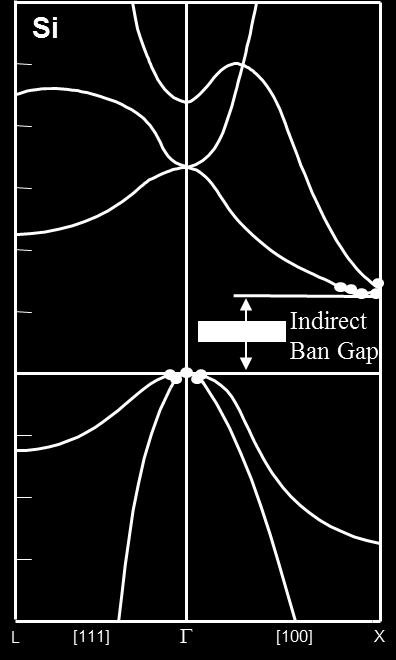
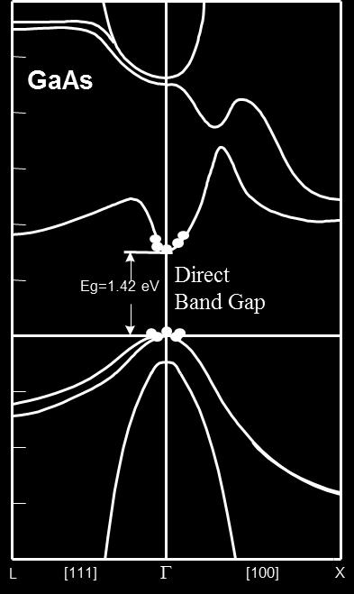
37 Direct and inderect band gap in semiconductors energy (E) and momentum (ħk) must be conserved energy is released when a quasi-free electron recombines with a hole in the valence band: ΔE = E g does this energy produce light (photon) or heat (phonon)? indirect bandgap: ΔK is large but for a direct bandgap: ΔK=0 photons have very low momentum but lattice vibrations (heat, phonons) have large momentum Conclusion: recombination (e - +h + ) creates light in direct bandgap materials (GaAs, GaN, etc) heat in indirect bandgap materials (Si, Ge)
38 Motion of free electrons Consider free electron E(p) Dispersion relation E p / m =( p + p + p ) / m pm v 0 x y z 0 0 Newton s law of motion Velocity Mass 0 dp p F x dt m 0 dr p dt p E E E E E v v= v xˆ v yˆ v zˆ xˆ yˆ zˆ p x x x y z m0 px px py pz E E E m 1 0 = px py pz
39 E Effective mass Taylor series near CB minimum 3 1 E E( k) E ( k k )( k k )... g i 0i j 0j i, j1 ki kj k ox k x k oy C.B. minimum k y Effective mass tensor k E E( k) E ( k k )( k k )... g i 0i j 0 j i, j1kikj 1 E m p p... p ( k k ) 3 1 g c, ij i j i i 0i i, j1 m 1 1 c, ij E kk i j
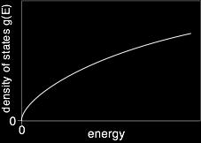
40 Density of states k z Parallelepiped of Volume V=L x L y L z Allowed states satisfy boundary conditions: k L pn i i i k y k x Each state occupies volume in k space V 8 p /( L L L ) 8p V k x y z Consider a conduction valley along x or [100] direction k E( k) Eg m m m kx y kz L T T k k x y kz 1 m ( E E ) m ( E E ) m ( E E ) L g T g T g Half axes m ( E E ) m ( E E ) m ( E E ) a, a =, a = ; L g T g T g x y z The volume in k-space containing energies less than E 3/ 4 4 1/ 3/ k ( ) p x y z p ( ) L T g V E a a a m m E E 3 3
41 Density of states k z 3/ 4 1/ 3/ k ( ) p ( ) L T g V E m m E E 3 k x Number of states with energies less than E k y 3/ V 1/ 3/ k k L T c N( E) V ( E) / V m m ( E E ) 3p Multiply by number of valleys -G, divide by volume take derivative 3/ * 3/ N( E) 1 G 1/ 1/ 1 m n 1/ c( ) ( ) ( ) L T g g g E G V m m E E E E E p p Number of states per unit volume per unit energy density of states Effective D.O.S. mass m * G /3 m m 1/3 n L T In GaAs m * n m c
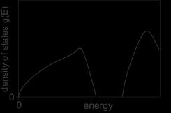
42 Density of states in the valence band k Count energy down E 3/ 3/ * 3/ * m lh 1/ m m hh 1/ p 1/ gv( E) glh( E) ghh( E) E E E p p p * 3/ 3/ Effective D.O.S. mass is /3 m m m ~ m p hh lh hh
43 Lecture 18: Energy bands in periodic crystalls Origin of the band gap and Bloch theorem Kronig-Penney model Empty lattice approximation Number of states in a band and filing of the bands Interpretation of the effective mass Effective mass method for hydrogen-like impurities in semiconductors
44 Hydrogen like impurities in semiconductors P donor in Si can be modeled d as hydrogen-like atom Hydrogen atom Hydrogen-like donor
45 Hydrogen atom - Bohr model ) (4 ) (4 energy: Total 4 1 Kineticenergy: 4 4 Potentialenergy: ) ( 4 4 1,,3..., for 4 1 n e mz E K r Ze V K E r Ze mv K r Ze dr r Ze V n Ze mr n v mze n r mr n mr n mr r mv Ze n n mvr L r v m r Ze r p p p p p p p p p p p
46 Hydrogen atom - Bohr model E 4 m0 q H. (4p0) 13 6 ev
47 Hydrogen like impurities in semiconductors Hydrogen-like donor Instead of m 0, we have to use m n*. Instead of o, we have to use K s o. K s is the relative dielectric constant of Si (K s, Si = 11.8). E 4 m0 q H. (4p0) 13 6 ev E d m * n 4 q (4π K ) s ev m * n m0 0 Ks ev
48 Lecture schedule (based on P.Hofmann s Solid State Physics,chapters 1-7 and 11) Module I Periodic Structures and Defects 0/1 Introduction. Crystal bonding. Periodicity and lattices, reciprocal space 4h 1/1 Laue condition, Ewald construction, interpretation of a diffraction experimen h /1 Bragg planes and Brillouin zones (BZ) h 3/1 Elastic strain and structural defects h 3/1 Atomic diffusion and summary of Module I h Module II - Phonons 03/ Vibrations, phonons, density of states, and Planck distribution 4h 04/ Lattice heat capacity: Dulong-Petit, Einstien and Debye models h 05/ Comparison of different models h 06/ Thermal conductivity h 07/ Thermal expansion and summary of Module II h Module III Electrons 4/ Free electron gas (FEG) versus Free electron Fermi gas (FEFG) 4h 5/ Effect of temperature Fermi- Dirac distribution h 6/ FEFG in D and 1D, and DOS in nanostructures h 7/ Origin of the band gap and nearly free electron model h 8/ Number of orbitals in a band and general form of the electronic states h Module IV Semiconductors 10/3 Energy bands and effective mass method 4h 11/3 Energy band structure (continuation) h 1/3 Intrinsic semiconductors h 13/3 Impurity states in semiconductors and carrier statistics h 14/3 p-n junctions and optoelectronic devices h
49 Lecture 19: Energy band structure (continuation) Dynamics of electrons in a band Band-to-band transitions
50 Dynamics of electrons in a band The external electric field causes a change in the k vectors of all electrons: dk d k e E F ee dt dt E If the electrons are in a partially filled band, this will break the symmetry of electron states in the 1 st BZ and produce a net current. But if they are in a filled band, even though all electrons change k vectors, the symmetry remains, so J = 0. p a v p a k x k x When an electron reaches the 1 st BZ edge (at k = p/a) it immediately reappears at the opposite edge (k = -p/a) and continues to increase its k value. As an electron s k value increases, its velocity increases, then decreases to zero and then becomes negative when it re-emerges at k = -p/a!!
51 Dynamics of electrons in a band
52 Band-to-band transitions 5
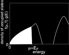
53 Band-to-band transitions valence band conduction band
54 Band-to-band transitions valence band conduction band gap size (ev) InSb 0.18 InAs 0.36 Ge 0.67 Si 1.11 GaAs 1.43 SiC.3 diamond 5.5 MgF 11


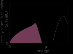
55 Band-to-band transitions valence band conduction band
56 Band-to-band transitions electrons in the conduction band (CB) missing electrons (holes) in the valence band (VB)
57 Band-to-band transitions
58 Band-to-band transitions free electrons VB maximum as E=0 conduction band valence band
59 Band-to-band transitions electrons in the conduction band (CB) missing electrons (holes) in the valence band (VB)
60 Band-to-band transitions for the conduction band for the valence band Both are Boltzmann distributions! This is called the non-degenerate case.
61 Band-to-band transitions
62 Band-to-band transitions CBM μ VBM
63 Band-to-band transitions In quantum wells
64 FYS Vår 014 (Kondenserte fasers fysikk) Pensum: Solid State Physics by Philip Hofmann (Chapters 1-7 and 11) Andrej Kuznetsov delivery address: Department of Physics, PB 1048 Blindern, 0316 OSLO Tel: , e-post: andrej.kuznetsov@fys.uio.no visiting address: MiNaLab, Gaustadaleen 3c
65 Lecture schedule (based on P.Hofmann s Solid State Physics,chapters 1-7 and 11) Module I Periodic Structures and Defects 0/1 Introduction. Crystal bonding. Periodicity and lattices, reciprocal space 4h 1/1 Laue condition, Ewald construction, interpretation of a diffraction experimen h /1 Bragg planes and Brillouin zones (BZ) h 3/1 Elastic strain and structural defects h 3/1 Atomic diffusion and summary of Module I h Module II - Phonons 03/ Vibrations, phonons, density of states, and Planck distribution 4h 04/ Lattice heat capacity: Dulong-Petit, Einstien and Debye models h 05/ Comparison of different models h 06/ Thermal conductivity h 07/ Thermal expansion and summary of Module II h Module III Electrons 4/ Free electron gas (FEG) versus Free electron Fermi gas (FEFG) 4h 5/ Effect of temperature Fermi- Dirac distribution h 6/ FEFG in D and 1D, and DOS in nanostructures h 7/ Origin of the band gap and nearly free electron model h 8/ Number of orbitals in a band and general form of the electronic states h Module IV Semiconductors 10/3 Energy bands and effective mass method 4h 11/3 Energy bands (continuation) h 1/3 Intrinsic semiconductors h 13/3 Impurity states in semiconductors and carrier statistics h 14/3 p-n junctions and optoelectronic devices h
66 Lecture 1: Impurity states in semiconductors and carrier statistics Intrinsic and extrinsic semiconductors hydrogen-like impurities n- and p-type semiconductors equilibrium charge carrier concentration carriers in non-eqilibrium conditions: diffusion, generation and recombination
67 Lecture 1: Impurity states in semiconductors and carrier statistics Intrinsic and extrinsic semiconductors hydrogen-like impurities n- and p-type semiconductors equilibrium charge carrier concentration carriers in non-eqilibrium conditions: diffusion, generation and recombination
68 Intrinsic and extrinsic semiconductors
69 Intrinsic and extrinsic semiconductors E g n i E i E g n 0 E i E g n 0 E i p i p 0 p 0
70 Intrinsic and extrinsic semiconductors n 0 E g E ID n d E d E i p 0
71 Lecture 1: Impurity states in semiconductors and carrier statistics Intrinsic and extrinsic semiconductors hydrogen-like impurities n- and p-type semiconductors equilibrium charge carrier concentration carriers in non-eqilibrium conditions: diffusion, generation and recombination

72 Hydrogen like impurities in semiconductors d P donor in Si can be modeled as hydrogen-like atom Hydrogen atom Hydrogen-like donor
73 Hydrogen atom - Bohr model ) (4 ) (4 energy: Total 4 1 Kineticenergy: 4 4 Potentialenergy: ) ( 4 4 1,,3..., for 4 1 n e mz E K r Ze V K E r Ze mv K r Ze dr r Ze V n Ze mr n v mze n r mr n mr n mr r mv Ze n n mvr L r v m r Ze r p p p p p p p p p p p
74 Hydrogen atom - Bohr model E 4 m0 q H. (4p0) 13 6 ev
75 Hydrogen like impurities in semiconductors Hydrogen-like donor Instead of m 0, we have to use m n*. Instead of o, we have to use K s o. K s is the relative dielectric constant of Si (K s, Si = 11.8). E 4 m0 q H. (4p0) 13 6 ev E d m * n 4 q (4π K ) s ev m * n m0 0 Ks ev
76 Hydrogen like impurities in semiconductors n 0 =0 n 0 E g E ID E g E ID E i E d n d E i E d p 0 =0 p 0
77 Lecture 1: Impurity states in semiconductors and carrier statistics Intrinsic and extrinsic semiconductors hydrogen-like impurities n- and p-type semiconductors equilibrium charge carrier concentration carriers in non-eqilibrium conditions: diffusion, generation and recombination
78 N- and p-type semiconductors Intrinsic semiconductor a) Energy level diagrams showing the excitation of an electron from the valence band to the conduction band. The resultant free electron can freely move under the application of electric field. b) Equal electron & hole concentrations in an intrinsic semiconductor created by the thermal excitation of electrons across the band gap
79 N- and p-type semiconductors n-type Semiconductor a) Donor level in an n-type semiconductor. b) The ionization of donor impurities creates an increased electron concentration distribution.
80 N- and p-type semiconductors p-type Semiconductor a) Acceptor level in an p-type semiconductor. b) The ionization of acceptor impurities creates an increased hole concentration distribution
81 N- and p-type semiconductors
82 N- and p-type semiconductors Intrinsic material: A perfect material with no impurities. n p n n& p & n i i E exp( k g B ) T are the electron, hole & intrinsic concentrations respectively. E g is the gap energy, T is Temperature. Extrinsic material: donor or acceptor type semiconductors. pn n i Majority carriers: electrons in n-type or holes in p-type. Minority carriers: holes in n-type or electrons in p-type.
83 N- and p-type semiconductors donor: impurity atom that increases n acceptor: impurity atom that increases p N-type material: contains more electrons than holes P-type material: contains more holes than electrons majority carrier: the most abundant carrier minority carrier: the least abundant carrier intrinsic semiconductor: n = p = n i extrinsic semiconductor: doped semiconductor
84 Lecture 1: Impurity states in semiconductors and carrier statistics Intrinsic and extrinsic semiconductors hydrogen-like impurities n- and p-type semiconductors equilibrium charge carrier concentration carriers in non-eqilibrium conditions: diffusion, generation and recombination
85 Equilibrium charge carrier concentration in semiconductors Consider conditions for charge neutrality. The net charge in a small portion of a uniformly doped semiconductor should be zero. Otherwise, there will be a net flow of charge from one point to another resulting in current flow (that is against out assumption of thermal equilibrium). Charge/cm 3 = q p q n + q N D + q N A = 0 or p n + N D + N A = 0 where N D + = # of ionized donors/cm 3 and N A = # of ionized acceptors per cm 3. Assuming total ionization of dopants, we can write:
86 Equilibrium charge carrier concentration in semiconductors Assume a non-degenerately doped semiconductor and assume total ionization of dopants. Then, n p = n i ; electron concentration hole concentration = n i p n + N D N A = 0; net charge in a given volume is zero. Solve for n and p in terms of N D and N A We get: (n i / n) n + N D N A = 0 n n (N D N A ) n i = 0 Solve this quadratic equation for the free electron concentration, n. From n p = n i equation, calculate free hole concentration, p.
87 Equilibrium charge carrier concentration in semiconductors Intrinsic semiconductor: N D = 0 and N A = 0 p = n = n i Doped semiconductors where N D N A >> n i n = N D N A ; p = n i / n if N D > N A p = N A N D ; n = n i / p if N A > N D Compensated semiconductor n = p = n i when n i >> N D N A When N D N A is comparable to n i,, we need to use the charge neutrality equation to determine n and p.
88 Equilibrium charge carrier concentration in semiconductors Example Si is doped with As Atom/cm 3. What is the equilibrium hole concentra-tion p 0 at 300 K? Where is E F relative to E i ni p0 10 n cm 17 n 0 n e i ( E F E i ) kt 17 n 10 EF Ei ktln ln eV 10 n i
89 Equilibrium charge carrier concentration in semiconductors n N p N 0 a 0 d
90 Lecture 1: Impurity states in semiconductors and carrier statistics Intrinsic and extrinsic semiconductors hydrogen-like impurities n- and p-type semiconductors equilibrium charge carrier concentration carriers in non-eqilibrium conditions: diffusion, generation and recombination
91 Charge carriers in non-eqilibrium conditions Particles diffuse from regions of higher concentration to regions of lower concentration region, due to random thermal motion.
92 Charge carriers in non-eqilibrium conditions J n,diff qd n dn dx J p,diff qd p dp dx D is the diffusion constant, or diffusivity.
93 Charge carriers in non-eqilibrium conditions J J J n p J n J n, drift J n, diff qn ε n qd n dn dx J p J p, drift J p, diff qp ε p qd p dp dx
94 Charge carriers in non-eqilibrium conditions The position of E F relative to the band edges is determined by the carrier concentrations, which is determined by the net dopant concentration. In equilibrium E F is constant; therefore, the band-edge energies vary with position in a non-uniformly doped semiconductor: E c (x) E F E v (x)
95 The ratio of carrier densities at two points depends exponentially on the potential difference between these points: 1 i i1 1 1 i 1 i i i1 i F i i 1 F i1 i 1 i1 F ln 1 ln ln ln Therefore ln Similarly, ln ln n n q kt E E q V V n n kt n n n n kt E E n n kt E E n n kt E E n n kt E E Charge carriers in non-eqilibrium conditions
96 E v (x) Charge carriers in non-eqilibrium conditions E f E c (x) Consider a piece of a non-uniformly doped semiconductor: n-type semiconductor Decreasing donor concentration E c (x) E F E v (x) n dn dx Nc e kt N e c n kt n kt ( E E ( Ec EF ) / kt de dx c qε c F )/ kt de dx c
97 Charge carriers in non-eqilibrium conditions If the dopant concentration profile varies gradually with position, then the majority-carrier concentration distribution does not differ much from the dopant concentration distribution. N x) p( x) N ( x) n( x) D( A n-type material: p-type material: n( x) ND( x) NA p( x) NA( x) ND ( x) ( x) kt q 1 n dn dx kt q 1 N D dn dx D in n-type material
98 Charge carriers in non-eqilibrium conditions Band-to-Band R-G Center Impact Ionization
99 Charge carriers in non-eqilibrium conditions Direct R-G Center Auger
100 Charge carriers in non-eqilibrium conditions Energy (E) vs. momentum (ħk) Diagrams Direct: Indirect: Little change in momentum is required for recombination momentum is conserved by photon emission Large change in momentum is required for recombination momentum is conserved by phonon + photon emission
101 Charge carriers in non-eqilibrium conditions equilibrium values n n n 0 p p p 0 Charge neutrality condition: n p
102 Charge carriers in non-eqilibrium conditions Often the disturbance from equilibrium is small, such that the majority-carrier concentration is not affected significantly: For an n-type material: n p n0 so n n0 For a p-type material: n p p0 so p p0 However, the minority carrier concentration can be significantly affected.
103 Charge carriers in non-eqilibrium conditions Consider a semiconductor with no current flow in which thermal equilibrium is disturbed by the sudden creation of excess holes and electrons. n t n n for electrons in p-type material p t p p for holes in n-type material
104 Charge carriers in non-eqilibrium conditions Uniformly doped p-type and n- type semiconductors before the junction is formed. Internal electric-field occurs in a depletion region of a p-n junction in thermal equilibrium
FYS Vår 2017 (Kondenserte fasers fysikk)
") FYS3410 - Vår 2017 (Kondenserte fasers fysikk) http://www.uio.no/studier/emner/matnat/fys/fys3410/v16/index.html Pensum: Introduction to Solid State Physics by Charles Kittel (Chapters 1-9, 11, 17, 18,
FYS3410 - Vår 2017 (Kondenserte fasers fysikk) http://www.uio.no/studier/emner/matnat/fys/fys3410/v16/index.html Pensum: Introduction to Solid State Physics by Charles Kittel (Chapters 1-9, 11, 17, 18,
FYS Vår 2015 (Kondenserte fasers fysikk)
") FYS410 - Vår 015 (Kondenserte fasers fysikk) http://www.uio.no/studier/emner/matnat/fys/fys410/v15/index.html Pensum: Introduction to Solid State Physics by Charles Kittel (Chapters 1-9 and 17, 18, 0)
FYS410 - Vår 015 (Kondenserte fasers fysikk) http://www.uio.no/studier/emner/matnat/fys/fys410/v15/index.html Pensum: Introduction to Solid State Physics by Charles Kittel (Chapters 1-9 and 17, 18, 0)
Three Most Important Topics (MIT) Today
 Today") Three Most Important Topics (MIT) Today Electrons in periodic potential Energy gap nearly free electron Bloch Theorem Energy gap tight binding Chapter 1 1 Electrons in Periodic Potential We now know the
Three Most Important Topics (MIT) Today Electrons in periodic potential Energy gap nearly free electron Bloch Theorem Energy gap tight binding Chapter 1 1 Electrons in Periodic Potential We now know the
Direct and Indirect Semiconductor
 Direct and Indirect Semiconductor Allowed values of energy can be plotted vs. the propagation constant, k. Since the periodicity of most lattices is different in various direction, the E-k diagram must
Ch. 2: Energy Bands And Charge Carriers In Semiconductors
 Ch. 2: Energy Bands And Charge Carriers In Semiconductors Discrete energy levels arise from balance of attraction force between electrons and nucleus and repulsion force between electrons each electron
Minimal Update of Solid State Physics
 Minimal Update of Solid State Physics It is expected that participants are acquainted with basics of solid state physics. Therefore here we will refresh only those aspects, which are absolutely necessary
Basic cell design. Si cell
 Basic cell design Si cell 1 Concepts needed to describe photovoltaic device 1. energy bands in semiconductors: from bonds to bands 2. free carriers: holes and electrons, doping 3. electron and hole current:
PHYS485 Materials Physics
 5/11/017 PHYS485 Materials Physics Dr. Gregory W. Clar Manchester University LET S GO ON A (TEK)ADVENTURE! WHAT? TRIP TO A MAKER S SPACE IN FORT WAYNE WHEN? THURSDAY, MAY 11 TH @ 5PM WHERE? TEKVENTURE
EECS130 Integrated Circuit Devices
 EECS130 Integrated Circuit Devices Professor Ali Javey 8/30/2007 Semiconductor Fundamentals Lecture 2 Read: Chapters 1 and 2 Last Lecture: Energy Band Diagram Conduction band E c E g Band gap E v Valence
Charge Carriers in Semiconductor
 Charge Carriers in Semiconductor To understand PN junction s IV characteristics, it is important to understand charge carriers behavior in solids, how to modify carrier densities, and different mechanisms
The Semiconductor in Equilibrium
 Lecture 6 Semiconductor physics IV The Semiconductor in Equilibrium Equilibrium, or thermal equilibrium No external forces such as voltages, electric fields. Magnetic fields, or temperature gradients are
ELEMENTARY BAND THEORY
 ELEMENTARY BAND THEORY PHYSICIST Solid state band Valence band, VB Conduction band, CB Fermi energy, E F Bloch orbital, delocalized n-doping p-doping Band gap, E g Direct band gap Indirect band gap Phonon
Semiconductor Physics and Devices Chapter 3.
 Introduction to the Quantum Theory of Solids We applied quantum mechanics and Schrödinger s equation to determine the behavior of electrons in a potential. Important findings Semiconductor Physics and
Crystal Properties. MS415 Lec. 2. High performance, high current. ZnO. GaN
 Crystal Properties Crystal Lattices: Periodic arrangement of atoms Repeated unit cells (solid-state) Stuffing atoms into unit cells Determine mechanical & electrical properties High performance, high current
ECE 442. Spring, Lecture -2
 ECE 442 Power Semiconductor Devices and Integrated circuits Spring, 2006 University of Illinois at Chicago Lecture -2 Semiconductor physics band structures and charge carriers 1. What are the types of
Chapter 1 Overview of Semiconductor Materials and Physics
 Chapter 1 Overview of Semiconductor Materials and Physics Professor Paul K. Chu Conductivity / Resistivity of Insulators, Semiconductors, and Conductors Semiconductor Elements Period II III IV V VI 2 B
Density of states for electrons and holes. Distribution function. Conduction and valence bands
 Intrinsic Semiconductors In the field of semiconductors electrons and holes are usually referred to as free carriers, or simply carriers, because it is these particles which are responsible for carrying
L5: Surface Recombination, Continuity Equation & Extended Topics tanford University
 L5: Surface Recombination, Continuity Equation & Extended Topics EE 216 : Aneesh Nainani 1 Announcements Project Select topic by Jan 29 (Tuesday) 9 topics, maximum 4 students per topic Quiz Thursday (Jan
Semiconductor Device Physics
 1 Semiconductor Device Physics Lecture 3 http://zitompul.wordpress.com 2 0 1 3 Semiconductor Device Physics 2 Three primary types of carrier action occur inside a semiconductor: Drift: charged particle
Semiconductor Physics. Lecture 3
 Semiconductor Physics Lecture 3 Intrinsic carrier density Intrinsic carrier density Law of mass action Valid also if we add an impurity which either donates extra electrons or holes the number of carriers
Review of Semiconductor Physics
 Solid-state physics Review of Semiconductor Physics The daunting task of solid state physics Quantum mechanics gives us the fundamental equation The equation is only analytically solvable for a handful
ECE 340 Lecture 6 : Intrinsic and Extrinsic Material I Class Outline:
 ECE 340 Lecture 6 : Intrinsic and Extrinsic Material I Class Outline: Effective Mass Intrinsic Material Extrinsic Material Things you should know when you leave Key Questions What is the physical meaning
Course overview. Me: Dr Luke Wilson. The course: Physics and applications of semiconductors. Office: E17 open door policy
 Course overview Me: Dr Luke Wilson Office: E17 open door policy email: luke.wilson@sheffield.ac.uk The course: Physics and applications of semiconductors 10 lectures aim is to allow time for at least one
Session 5: Solid State Physics. Charge Mobility Drift Diffusion Recombination-Generation
 Session 5: Solid State Physics Charge Mobility Drift Diffusion Recombination-Generation 1 Outline A B C D E F G H I J 2 Mobile Charge Carriers in Semiconductors Three primary types of carrier action occur
Calculating Band Structure
 Calculating Band Structure Nearly free electron Assume plane wave solution for electrons Weak potential V(x) Brillouin zone edge Tight binding method Electrons in local atomic states (bound states) Interatomic
Lecture 15: Optoelectronic devices: Introduction
 Lecture 15: Optoelectronic devices: Introduction Contents 1 Optical absorption 1 1.1 Absorption coefficient....................... 2 2 Optical recombination 5 3 Recombination and carrier lifetime 6 3.1
n N D n p = n i p N A
 Summary of electron and hole concentration in semiconductors Intrinsic semiconductor: E G n kt i = pi = N e 2 0 Donor-doped semiconductor: n N D where N D is the concentration of donor impurity Acceptor-doped
SEMICONDUCTOR PHYSICS
 SEMICONDUCTOR PHYSICS by Dibyendu Chowdhury Semiconductors The materials whose electrical conductivity lies between those of conductors and insulators, are known as semiconductors. Silicon Germanium Cadmium
EECS143 Microfabrication Technology
 EECS143 Microfabrication Technology Professor Ali Javey Introduction to Materials Lecture 1 Evolution of Devices Yesterday s Transistor (1947) Today s Transistor (2006) Why Semiconductors? Conductors e.g
EE143 Fall 2016 Microfabrication Technologies. Evolution of Devices
 EE143 Fall 2016 Microfabrication Technologies Prof. Ming C. Wu wu@eecs.berkeley.edu 511 Sutardja Dai Hall (SDH) 1-1 Evolution of Devices Yesterday s Transistor (1947) Today s Transistor (2006) 1-2 1 Why
Chapter 3: Introduction to the Quantum Theory of Solids
 Chapter 3: Introduction to the Quantum Theory of Solids Determine the properties of electrons in a crystal lattice. Determine the statistical characteristics of the very large number of electrons in a
PHYS208 P-N Junction. Olav Torheim. May 30, 2007
 1 PHYS208 P-N Junction Olav Torheim May 30, 2007 1 Intrinsic semiconductors The lower end of the conduction band is a parabola, just like in the quadratic free electron case (E = h2 k 2 2m ). The density
ESE 372 / Spring 2013 / Lecture 5 Metal Oxide Semiconductor Field Effect Transistor
 Metal Oxide Semiconductor Field Effect Transistor V G V G 1 Metal Oxide Semiconductor Field Effect Transistor We will need to understand how this current flows through Si What is electric current? 2 Back
MTLE-6120: Advanced Electronic Properties of Materials. Intrinsic and extrinsic semiconductors. Reading: Kasap:
 MTLE-6120: Advanced Electronic Properties of Materials 1 Intrinsic and extrinsic semiconductors Reading: Kasap: 5.1-5.6 Band structure and conduction 2 Metals: partially filled band(s) i.e. bands cross
CHAPTER 2: ENERGY BANDS & CARRIER CONCENTRATION IN THERMAL EQUILIBRIUM. M.N.A. Halif & S.N. Sabki
 CHAPTER 2: ENERGY BANDS & CARRIER CONCENTRATION IN THERMAL EQUILIBRIUM OUTLINE 2.1 INTRODUCTION: 2.1.1 Semiconductor Materials 2.1.2 Basic Crystal Structure 2.1.3 Basic Crystal Growth technique 2.1.4 Valence
Energy bands in solids. Some pictures are taken from Ashcroft and Mermin from Kittel from Mizutani and from several sources on the web.
 Energy bands in solids Some pictures are taken from Ashcroft and Mermin from Kittel from Mizutani and from several sources on the web. we are starting to remind p E = = mv 1 2 = k mv = 2 2 k 2m 2 Some
Key Questions. ECE 340 Lecture 6 : Intrinsic and Extrinsic Material I 9/10/12. Class Outline: Effective Mass Intrinsic Material
 9/1/1 ECE 34 Lecture 6 : Intrinsic and Extrinsic Material I Class Outline: Things you should know when you leave Key Questions What is the physical meaning of the effective mass What does a negative effective
Chapter 1 Semiconductor basics
 Chapter 1 Semiconductor basics ELEC-H402/CH1: Semiconductor basics 1 Basic semiconductor concepts Semiconductor basics Semiconductors, silicon and hole-electron pair Intrinsic silicon properties Doped
Electron Energy, E E = 0. Free electron. 3s Band 2p Band Overlapping energy bands. 3p 3s 2p 2s. 2s Band. Electrons. 1s ATOM SOLID.
 Electron Energy, E Free electron Vacuum level 3p 3s 2p 2s 2s Band 3s Band 2p Band Overlapping energy bands Electrons E = 0 1s ATOM 1s SOLID In a metal the various energy bands overlap to give a single
Semiconductor physics I. The Crystal Structure of Solids
 Lecture 3 Semiconductor physics I The Crystal Structure of Solids 1 Semiconductor materials Types of solids Space lattices Atomic Bonding Imperfection and doping in SOLIDS 2 Semiconductor Semiconductors
Lecture 1. OUTLINE Basic Semiconductor Physics. Reading: Chapter 2.1. Semiconductors Intrinsic (undoped) silicon Doping Carrier concentrations
 silicon Doping Carrier concentrations") Lecture 1 OUTLINE Basic Semiconductor Physics Semiconductors Intrinsic (undoped) silicon Doping Carrier concentrations Reading: Chapter 2.1 EE105 Fall 2007 Lecture 1, Slide 1 What is a Semiconductor? Low
Lecture 1 OUTLINE Basic Semiconductor Physics Semiconductors Intrinsic (undoped) silicon Doping Carrier concentrations Reading: Chapter 2.1 EE105 Fall 2007 Lecture 1, Slide 1 What is a Semiconductor? Low
Chemistry Instrumental Analysis Lecture 8. Chem 4631
 Chemistry 4631 Instrumental Analysis Lecture 8 UV to IR Components of Optical Basic components of spectroscopic instruments: stable source of radiant energy transparent container to hold sample device
Introductory Nanotechnology ~ Basic Condensed Matter Physics ~
 Introductory Nanotechnology ~ Basic Condensed Matter Physics ~ Atsufumi Hirohata Department of Electronics Quick Review over the Last Lecture Classic model : Dulong-Petit empirical law c V, mol 3R 0 E
Chapter 4: Bonding in Solids and Electronic Properties. Free electron theory
 Chapter 4: Bonding in Solids and Electronic Properties Free electron theory Consider free electrons in a metal an electron gas. regards a metal as a box in which electrons are free to move. assumes nuclei
CME 300 Properties of Materials. ANSWERS: Homework 9 November 26, As atoms approach each other in the solid state the quantized energy states:
 CME 300 Properties of Materials ANSWERS: Homework 9 November 26, 2011 As atoms approach each other in the solid state the quantized energy states: are split. This splitting is associated with the wave
Introduction to Quantum Theory of Solids
 Lecture 5 Semiconductor physics III Introduction to Quantum Theory of Solids 1 Goals To determine the properties of electrons in a crystal lattice To determine the statistical characteristics of the very
Chapter 7. The pn Junction
 Chapter 7 The pn Junction Chapter 7 PN Junction PN junction can be fabricated by implanting or diffusing donors into a P-type substrate such that a layer of semiconductor is converted into N type. Converting
3. Two-dimensional systems
 3. Two-dimensional systems Image from IBM-Almaden 1 Introduction Type I: natural layered structures, e.g., graphite (with C nanostructures) Type II: artificial structures, heterojunctions Great technological
Variation of Energy Bands with Alloy Composition E
 Variation of Energy Bands with Alloy Composition E 3.0 E.8.6 L 0.3eV Al x GaAs AlAs 1- xas 1.43eV.16eV X k.4 L. X.0 X 1.8 L 1.6 1.4 0 0. 0.4 0.6 X 0.8 1 1 Carriers in intrinsic Semiconductors Ec 4º 1º
Solid State Device Fundamentals
 4. lectrons and Holes Solid State Device Fundamentals NS 45 Lecture Course by Alexander M. Zaitsev alexander.zaitsev@csi.cuny.edu Tel: 718 982 2812 4N101b 1 4. lectrons and Holes Free electrons and holes
Silicon. tetrahedron diamond structure
 Silicon a tetrahedron a a diamond structure Tetrahedral bonding Hund s Rule 14Si [e] 3s 3p [e] hybridize 3sp 3 Hybridized level has higher energy for an isolated atom, but allows overall reduction in energy
Lecture 8. Equations of State, Equilibrium and Einstein Relationships and Generation/Recombination
 Lecture 8 Equations of State, Equilibrium and Einstein Relationships and Generation/Recombination Reading: (Cont d) Notes and Anderson 2 sections 3.4-3.11 Energy Equilibrium Concept Consider a non-uniformly
SEMICONDUCTOR PHYSICS REVIEW BONDS,
 SEMICONDUCTOR PHYSICS REVIEW BONDS, BANDS, EFFECTIVE MASS, DRIFT, DIFFUSION, GENERATION, RECOMBINATION February 3, 2011 The University of Toledo, Department of Physics and Astronomy SSARE, PVIC Principles
Basic Principles of Light Emission in Semiconductors
 Basic Principles of Light Emission in Semiconductors Class: Integrated Photonic Devices Time: Fri. 8:00am ~ 11:00am. Classroom: 資電 06 Lecturer: Prof. 李明昌 (Ming-Chang Lee) Model for Light Generation and
Electrons, Holes, and Defect ionization
 Electrons, Holes, and Defect ionization The process of forming intrinsic electron-hole pairs is excitation a cross the band gap ( formation energy ). intrinsic electronic reaction : null e + h When electrons
Mark Lundstrom 2/10/2013. SOLUTIONS: ECE 606 Homework Week 5 Mark Lundstrom Purdue University (corrected 3/26/13)
") SOLUIONS: ECE 606 Homework Week 5 Mark Lundstrom Purdue University corrected 6/13) Some of the problems below are taken/adapted from Chapter 4 in Advanced Semiconductor Fundamentals, nd. Ed. By R.F. Pierret.
SOLUIONS: ECE 606 Homework Week 5 Mark Lundstrom Purdue University corrected 6/13) Some of the problems below are taken/adapted from Chapter 4 in Advanced Semiconductor Fundamentals, nd. Ed. By R.F. Pierret.
Chapter 12: Semiconductors
 Chapter 12: Semiconductors Bardeen & Shottky January 30, 2017 Contents 1 Band Structure 4 2 Charge Carrier Density in Intrinsic Semiconductors. 6 3 Doping of Semiconductors 12 4 Carrier Densities in Doped
The potential is minimum at the positive ion sites and maximum between the two ions.
 1. Bloch theorem: - A crystalline solid consists of a lattice, which is composed of a large number of ion cores at regular intervals, and the conduction electrons that can move freely through out the lattice.
EE 346: Semiconductor Devices
 EE 346: Semiconductor Devices Lecture - 6 02/06/2017 Tewodros A. Zewde 1 DENSTY OF STATES FUNCTON Since current is due to the flow of charge, an important step in the process is to determine the number
Solid State Device Fundamentals
 Solid State Device Fundamentals ES 345 Lecture Course by Alexander M. Zaitsev alexander.zaitsev@csi.cuny.edu Tel: 718 982 2812 Oice 4101b 1 The ree electron model o metals The ree electron model o metals
smal band gap Saturday, April 9, 2011
 small band gap upper (conduction) band empty small gap valence band filled 2s 2p 2s 2p hybrid (s+p)band 2p no gap 2s (depend on the crystallographic orientation) extrinsic semiconductor semi-metal electron
Spring 2010 MSE 111. Midterm Exam. Prof. Eugene E. Haller. University of California at Berkeley Department of Materials Science and Engineering
 Spring 00 MS Midterm xam Prof. ugene. Haller University of California at Berkeley Department of Materials Science and ngineering 3/6/0, 9:40 am 80 minutes, 74 points total, 0 pages ame: SID: Problem 3
Semiconductor device structures are traditionally divided into homojunction devices
 0. Introduction: Semiconductor device structures are traditionally divided into homojunction devices (devices consisting of only one type of semiconductor material) and heterojunction devices (consisting
Lecture 7: Extrinsic semiconductors - Fermi level
 Lecture 7: Extrinsic semiconductors - Fermi level Contents 1 Dopant materials 1 2 E F in extrinsic semiconductors 5 3 Temperature dependence of carrier concentration 6 3.1 Low temperature regime (T < T
Engineering 2000 Chapter 8 Semiconductors. ENG2000: R.I. Hornsey Semi: 1
 Engineering 2000 Chapter 8 Semiconductors ENG2000: R.I. Hornsey Semi: 1 Overview We need to know the electrical properties of Si To do this, we must also draw on some of the physical properties and we
1 Review of semiconductor materials and physics
 Part One Devices 1 Review of semiconductor materials and physics 1.1 Executive summary Semiconductor devices are fabricated using specific materials that offer the desired physical properties. There are
UConn ECE 4211, Semiconductor Devices and Nanostructures Lecture Week 1 January 17, 2017
 UConn ECE 411, Semiconductor Devices and Nanostructures Lecture Week 1 January 17, 017 Device Operation: One of the objectives of this course is to understand operation of carrier transport in semiconductor
Solid State Physics. Lecture 10 Band Theory. Professor Stephen Sweeney
 Solid State Physics Lecture 10 Band Theory Professor Stephen Sweeney Advanced Technology Institute and Department of Physics University of Surrey, Guildford, GU2 7XH, UK s.sweeney@surrey.ac.uk Recap from
Intrinsic Semiconductors
 Technische Universität Graz Institute of Solid State Physics Intrinsic Semiconductors ermi function f(e) is the probability that a state at energy E is occupied. f( E) 1 E E 1 exp kt B ermi energy The
Lecture 15 - The pn Junction Diode (I) I-V Characteristics. November 1, 2005
 I-V Characteristics. November 1, 2005") 6.012 - Microelectronic Devices and Circuits - Fall 2005 Lecture 15-1 Lecture 15 - The pn Junction Diode (I) I-V Characteristics November 1, 2005 Contents: 1. pn junction under bias 2. I-V characteristics
6.012 - Microelectronic Devices and Circuits - Fall 2005 Lecture 15-1 Lecture 15 - The pn Junction Diode (I) I-V Characteristics November 1, 2005 Contents: 1. pn junction under bias 2. I-V characteristics
Basic Semiconductor Physics
 6 Basic Semiconductor Physics 6.1 Introduction With this chapter we start with the discussion of some important concepts from semiconductor physics, which are required to understand the operation of solar
Semiconductor Physics
 1 Semiconductor Physics 1.1 Introduction 2 1.2 The Band Theory of Solids 2 1.3 The Kronig Penney Model 3 1.4 The Bragg Model 8 1.5 Effective Mass 8 1.6 Number of States in a Band 10 1.7 Band Filling 12
1 Name: Student number: DEPARTMENT OF PHYSICS AND PHYSICAL OCEANOGRAPHY MEMORIAL UNIVERSITY OF NEWFOUNDLAND. Fall :00-11:00
 1 Name: DEPARTMENT OF PHYSICS AND PHYSICAL OCEANOGRAPHY MEMORIAL UNIVERSITY OF NEWFOUNDLAND Final Exam Physics 3000 December 11, 2012 Fall 2012 9:00-11:00 INSTRUCTIONS: 1. Answer all seven (7) questions.
PHYS208 p-n junction. January 15, 2010
 1 PHYS208 p-n junction January 15, 2010 List of topics (1) Density of states Fermi-Dirac distribution Law of mass action Doped semiconductors Dopinglevel p-n-junctions 1 Intrinsic semiconductors List of
Lecture 2 Electrons and Holes in Semiconductors
 EE 471: Transport Phenomena in Solid State Devices Spring 2018 Lecture 2 Electrons and Holes in Semiconductors Bryan Ackland Department of Electrical and Computer Engineering Stevens Institute of Technology
Nearly Free Electron Gas model - I
 Nearly Free Electron Gas model - I Contents 1 Free electron gas model summary 1 2 Electron effective mass 3 2.1 FEG model for sodium...................... 4 3 Nearly free electron model 5 3.1 Primitive
Lecture 2. Semiconductor Physics. Sunday 4/10/2015 Semiconductor Physics 1-1
 Lecture 2 Semiconductor Physics Sunday 4/10/2015 Semiconductor Physics 1-1 Outline Intrinsic bond model: electrons and holes Charge carrier generation and recombination Intrinsic semiconductor Doping:
半導體元件與物理. Semiconductor Devices and physics 許正興國立聯合大學電機工程學系 聯大電機系電子材料與元件應用實驗室
 半導體元件與物理 Semiconductor Devices and physics 許正興國立聯合大學電機工程學系 1. Crystal Structure of Solids 2. Quantum Theory of Solids 3. Semiconductor in Equilibrium and Carrier Transport phenomena 4. PN Junction and
* motif: a single or repeated design or color
 Chapter 2. Structure A. Electronic structure vs. Geometric structure B. Clean surface vs. Adsorbate covered surface (substrate + overlayer) C. Adsorbate structure - how are the adsorbed molecules bound
Metal Semiconductor Contacts
 Metal Semiconductor Contacts The investigation of rectification in metal-semiconductor contacts was first described by Braun [33-35], who discovered in 1874 the asymmetric nature of electrical conduction
Electrical Resistance
 Electrical Resistance I + V _ W Material with resistivity ρ t L Resistance R V I = L ρ Wt (Unit: ohms) where ρ is the electrical resistivity 1 Adding parts/billion to parts/thousand of dopants to pure
Communications with Optical Fibers
 Communications with Optical Fibers In digital communications, signals are generally sent as light pulses along an optical fiber. Information is first converted to an electrical signal in the form of pulses
sin[( t 2 Home Problem Set #1 Due : September 10 (Wed), 2008
, 2008") Home Problem Set #1 Due : September 10 (Wed), 008 1. Answer the following questions related to the wave-particle duality. (a) When an electron (mass m) is moving with the velocity of υ, what is the wave
Home Problem Set #1 Due : September 10 (Wed), 008 1. Answer the following questions related to the wave-particle duality. (a) When an electron (mass m) is moving with the velocity of υ, what is the wave
Lecture 2. Unit Cells and Miller Indexes. Reading: (Cont d) Anderson 2 1.8,
 Anderson 2 1.8,") Lecture 2 Unit Cells and Miller Indexes Reading: (Cont d) Anderson 2 1.8, 2.1-2.7 Unit Cell Concept The crystal lattice consists of a periodic array of atoms. Unit Cell Concept A building block that can
Lecture 2 Unit Cells and Miller Indexes Reading: (Cont d) Anderson 2 1.8, 2.1-2.7 Unit Cell Concept The crystal lattice consists of a periodic array of atoms. Unit Cell Concept A building block that can
Review of Optical Properties of Materials
 Review of Optical Properties of Materials Review of optics Absorption in semiconductors: qualitative discussion Derivation of Optical Absorption Coefficient in Direct Semiconductors Photons When dealing
Introduction to Sources: Radiative Processes and Population Inversion in Atoms, Molecules, and Semiconductors Atoms and Molecules
 OPTI 500 DEF, Spring 2012, Lecture 2 Introduction to Sources: Radiative Processes and Population Inversion in Atoms, Molecules, and Semiconductors Atoms and Molecules Energy Levels Every atom or molecule
KATIHAL FİZİĞİ MNT-510
 KATIHAL FİZİĞİ MNT-510 YARIİLETKENLER Kaynaklar: Katıhal Fiziği, Prof. Dr. Mustafa Dikici, Seçkin Yayıncılık Katıhal Fiziği, Şakir Aydoğan, Nobel Yayıncılık, Physics for Computer Science Students: With
Bohr s Model, Energy Bands, Electrons and Holes
 Dual Character of Material Particles Experimental physics before 1900 demonstrated that most of the physical phenomena can be explained by Newton's equation of motion of material particles or bodies and
5 Problems Chapter 5: Electrons Subject to a Periodic Potential Band Theory of Solids
 E n = :75, so E cont = E E n = :75 = :479. Using E =!, :479 = m e k z =! j e j m e k z! k z = r :479 je j m e = :55 9 (44) (v g ) z = @! @k z = m e k z = m e :55 9 = :95 5 m/s. 4.. A ev electron is to
CLASS 12th. Semiconductors
 CLASS 12th Semiconductors 01. Distinction Between Metals, Insulators and Semi-Conductors Metals are good conductors of electricity, insulators do not conduct electricity, while the semiconductors have
8.1 Drift diffusion model
 8.1 Drift diffusion model Advanced theory 1 Basic Semiconductor Equations The fundamentals of semiconductor physic are well described by tools of quantum mechanic. This point of view gives us a model of
collisions of electrons. In semiconductor, in certain temperature ranges the conductivity increases rapidly by increasing temperature
 1.9. Temperature Dependence of Semiconductor Conductivity Such dependence is one most important in semiconductor. In metals, Conductivity decreases by increasing temperature due to greater frequency of
Peak Electric Field. Junction breakdown occurs when the peak electric field in the PN junction reaches a critical value. For the N + P junction,
 Peak Electric Field Junction breakdown occurs when the peak electric field in the P junction reaches a critical value. For the + P junction, qa E ( x) ( xp x), s W dep 2 s ( bi Vr ) 2 s potential barrier
Carriers Concentration in Semiconductors - V. Prof.P. Ravindran, Department of Physics, Central University of Tamil Nadu, India
 Carriers Concentration in Semiconductors - V 1 Prof.P. Ravindran, Department of Physics, Central University of Tamil Nadu, India http://folk.uio.no/ravi/semi2013 Motion and Recombination of Electrons and
Draft of solution Exam TFY4220, Solid State Physics, 29. May 2015.
 Draft of solution Exam TY40, Solid State Physics, 9. May 05. Problem (5%) Introductory questions (answers can be found in the books) a) Small Ewald sphere, not many reflections in Bragg with a single crystal.
Introduction to Semiconductor Physics. Prof.P. Ravindran, Department of Physics, Central University of Tamil Nadu, India
 Introduction to Semiconductor Physics 1 Prof.P. Ravindran, Department of Physics, Central University of Tamil Nadu, India http://folk.uio.no/ravi/cmp2013 Review of Semiconductor Physics Semiconductor fundamentals
LEC E T C U T R U E R E 17 -Photodetectors
 LECTURE 17 -Photodetectors Topics to be covered Photodetectors PIN photodiode Avalanche Photodiode Photodetectors Principle of the p-n junction Photodiode A generic photodiode. Photodetectors Principle
Chapter Two. Energy Bands and Effective Mass
 Chapter Two Energy Bands and Effective Mass Energy Bands Formation At Low Temperature At Room Temperature Valence Band Insulators Metals Effective Mass Energy-Momentum Diagrams Direct and Indirect Semiconduction
Classification of Solids
 Classification of Solids Classification by conductivity, which is related to the band structure: (Filled bands are shown dark; D(E) = Density of states) Class Electron Density Density of States D(E) Examples
ECE 250 Electronic Devices 1. Electronic Device Modeling
 ECE 250 Electronic Devices 1 ECE 250 Electronic Device Modeling ECE 250 Electronic Devices 2 Introduction to Semiconductor Physics You should really take a semiconductor device physics course. We can only