Solar Photovoltaics under Partially Shaded Conditions. Vivek Agarwal Dept of Electrical Engineering
|
|
|
- Andrea Smith
- 5 years ago
- Views:
Transcription

1 Solar Photovoltaics under Partially Shaded Conditions Vivek Agarwal Dept of Electrical Engineering
2 Neils Bohr s Atomic Model Increasing energy orbits n = 1 n = 2 n = 3 A photon is absorbed with energy, E = hυ Electrons in atoms orbit the nucleus in stationary orbits where it does not radiate. Electrons can only gain and lose energy by jumping from one allowed orbit to another, absorbing or emitting electromagnetic radiation with a frequency ν determined by the energy difference of the levels according to the Plank s relation. A photon is emitted with energy, E = hυ E = h (h=plank s constant and = frequency of the radiation.)
3 Different types of materials according to their conductivity Conductors Semiconductors Insulators Resistivity: 10-5 Ω-m Resistivity: 10-5 Ω-m to 10 5 Ω-m Resistivity: More than 10 5 Ω-m Example: Copper Example: Silicon, Ge Example: Teflon
4 Energy Energy Energy Energy band theory in different materials Conduction band Band gap Valence band Conduction band Band gap Valence band Conduction band Valence band Insulators Semiconductors Conductors If energy gap is high it is difficult for electrons to jump to the conduction band. Then there will be less electrons in the conduction band which adversely affects the conductivity. However, if the band gap is small or the bands are overlapping there will be higher conductivity
5 P-n junction diode Anode P- type material n- type material Cathode A semiconductor material is doped in such a way that a boundary interface is created between a p type and an n type material. This is called a p-n Junction diode They allow flow of current in only one direction These are widely used in signal level and power level electronics.
6 Extrinsic and Intrinsic semiconductors Intrinsic Semiconductors: These are the pure and undoped semiconductors. Extrinsic semiconductors: These are the doped semiconductors with higher conductivity.

7 Photoelectric effect According to photo electric effect, if a light of certain frequency, is incident upon a metal surface, electrons are emitted. The energy carried by each light particle is, E=h, where h is plank s constant and is the frequency of light. According to Einstein, the complete energy of the photon is transferred to the electron. photon e e e e e e e e e e e e e e e e Metal e Electron e e e e e
8 Current (A) Current (A) Solar Photovoltaic cell working principle and characteristics Electron flow photon photon I e e Front electrical contact N-type material Depletion region Not illuminated cell V oc V electron e Whole P-type material Back electrical contact Photon absorbed in depletion region and creation of electron whole Under illumination I sc Standard operating region of the I-V curve of a PV cell Maximum Power Point (MPP) Power (W) Short circuit current I sc Maximum Power Point (MPP) Open circuit voltage (V oc ) Voltage (V) Voltage (V)


9 PV Cell- PV Module- PV Arrays PV Cell PV Module PV Array Generates electricity from solar energy using photovoltaic effect PV cells are connected and sealed to form modules Modules are connected in series and parallel for required voltage and current rating
10 Current (A) Maximum Power Point Tracking (MPPT) PV characteristics MPP R 1 PV DC to DC converter Load I R 2 Load characteristics V By varying the load curve MPP is achieved This is done using a power converter Voltage (V) Maximum Power Point (MPP) Power (W)
11 Partial Shading Condition Shaded module 1 Shaded module 2 Power output is reduced local hotspot problem Solution? Shaded module 1 Shaded module 2 Bypass Diodes Unshaded Module provide Power Not shaded module Not shaded module
12 M o d u le 2 B y p a s s d io d e s M o d u le 1
13 C u rre n t (A ) P o w e r (W ) (V 3,P 3 ) (V 2,P 2 ) I 3 V 3 I 2 V 2 I 1 V V o lta g e (V ) (V 10 1,P 1 ) V o lta g e (V ) Resultant characteristics of two series connected modules. (a) I-V characteristics and (b) P-V characteristics.


14 MPPT during Partial Shading Generation of multiple peaks in the powervoltage characteristics with Bypass Diode Un-shaded modules continue to provide the power Loss of power that a shaded module could have generated anyhow
15 MPPT during Partial Shading i str-max MPPT i str-max -i PV1 i PV1 v 1 DC-DC Conv C out vpv(out) Load i str-max -i PVn i PVn v n DC-DC Conv
16 C u rre n t (A ) M o d u le -1 M o d u le 2 3 B y p a s s d io d e s I 3 M o d u le -2 M o d u le I 2 I 1 V 23 V 22 V 13 V 12 V 21 V V o lta g e (V ) Series connected modules with bypass diodes
17 C u rre n t (A ) P o w e r (W ) (V 3,P 3 ) (V 2,P 2 ) I 3 V 3 I 2 V 2 I 1 V V o lta g e (V ) (V 10 1,P 1 ) V o lta g e (V ) Resultant characteristics of the two series connected modules. (a) I-V characteristics and (b) P-V characteristics.
18 C u rre n t (A ) C u rre n t (A ) 4 (V O 1,I A 1 ) (V O 2,I A 2 ) 3.5 B lo c k in g d io d e s 3 G = 0.25 M o d u le 2 M o d u le 4 M o d u le B y p a s s d io d e s (V O 1,I B 1 ) R e s u lta n t I-V c u rv e fo r s e rie s c o n n e c te d m o d u le s 3 a n d 4 (V O 3,I A 3 ) G = 1 M o d u le R e s u lta n t I -V c u rv e fo r s e rie s c o n n e c te d m o d u le s 1 a n d 2 (V O 2,I B 2 ) (V O 3,I B 3 ) V o lta g e (V ) B lo c k in g d io d e s (V O 1,I A 1 ) (V O 2,I A 2 ) G = 0.25 M o d u le 2 G = 1 M o d u le 1 M o d u le 4 M o d u le 3 B y p a s s d io d e s (V O 1,I B 1 ) R e s u lta n t I-V c u rv e fo r s e rie s c o n n e c te d m o d u le s 3 a n d 4 (V O 2,I B 2 ) R e s u lta n t I -V c u rv e fo r (V O 3,I A 3 ) 0.5 s e rie s c o n n e c te d m o d u le s 1 a n d 2 (V O 3,I B 3 ) V o lta g e (V )
19 C u rre n t (A ) P o w e r (W ) P O 2 L o c a l P e a k G lo b a l P e a k 7 6 (V O 1,I O 1 ) 100 P O 1 5 (V O 2,I O 2 ) V o lta g e (V ) (V O 3,I O 3 ) 50 P O 3 V O 1 V O 2 V O V o lta g e (V ) (a ) (b )
20 Modelling of Partial Shading There is a need for a flexible, interactive, and comprehensive simulation model, which can serve as the following. A basic tool to accurately predict the PV characteristics and output power under partially shaded conditions. A design aid for users who want to build actual PV systems, study the stability and interfacing aspects. A tool to study the effect of array configuration on the output power for a likely/known shading pattern. A planning tool that can help in the installation of efficient and optimum PV arrays in a given surrounding. And a tool to develop and validate the effectiveness of existing and new MPPT schemes. Software packages like PV-Spice, PV-DesignPro, SolarPro, PVcad, and PVsyst are available, but have one or more of the following limitations: commercial, proprietary in nature and expensive; too complex to model the shading effects; do not support the interfacing of the PV arrays with actual power electronic systems.
21 PV cell G1 G2 G3 G4 PV cell S2 (a) S1 (a) (b) (c) Shading PV array terminologies (a) A PV module; (b) A series-assembly of two series connected sub-assemblies S1 and S2; (c) A group; (d) A PV array with groups G1 to G4. (d)
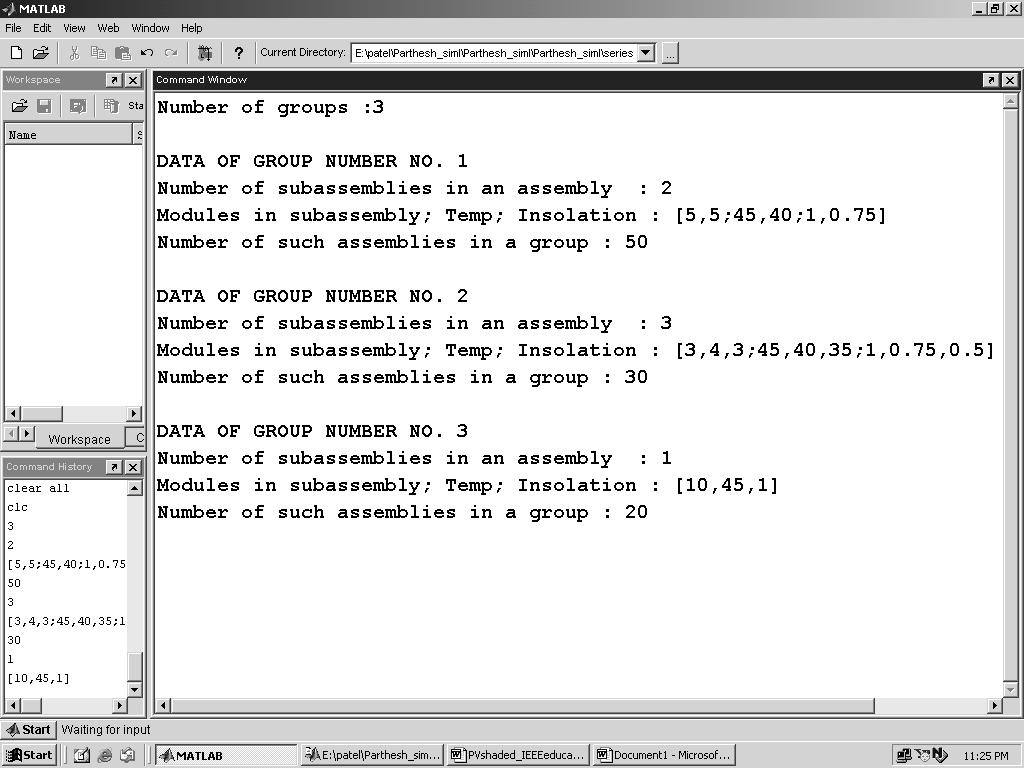
22 G1 G2 G3 Modules 1 to 10 1 To 40 1 To 38 1 To 22 Group Number of unshaded modules in series assembly (λ=1) Number of shaded modules in series assembly (λ=0.1) No. of series assemblies in a group G G G
 are described to the software.")
23 Modelling of Partial Shading: Simulation procedure The tool can simulate the array characteristics, for any value of temperature, insolation, and for any array configuration, with and without the bypass and blocking diodes. Via a MATLAB command window the given array configuration, temperature, and the insolation level(s) are described to the software. The matrix U of size G 3, where G is the number of groups, represents the array configuration. Each row indicates a group with a particular shading pattern on the series assemblies within that group. The elements of each row represent the number of unshaded and shaded modules, respectively, in a series assembly, and the number of such series assemblies in the group.

24 Modelling of Partial Shading: Simulation procedure Once the information is fed into the software, various windows pop up on the monitor. These windows display the I V and P V characteristics of different components of the PV array.
25 Modelling of Partial Shading: Simulation procedure If two PV modules are connected in series, they will conduct the same current, but the voltage across them will be different. In order to obtain the I V characteristics of the series-connected modules (series assembly) conducting a current Io, the voltages across these modules, V1 and V2, are added to determine the resultant output voltage. The characteristics for series assembly are, thus, obtained internally by the software by applying similar procedure at all the points on the I V curve of the series-connected modules.
26 Modelling of Partial Shading A MATLAB-based modeling and simulation scheme suitable for studying the I V and P V characteristics of a PV array under a non-uniform insolation due to partial shading. Scope for developing and evaluating new MPPT techniques, especially for partially shaded conditions. The proposed models interface with the models of power electronic converters, which is a very useful feature. It can also be used as a tool to study the effects of shading patterns on PV panels having different configurations.
27 Generalized Modeling
28 [a] Patel, H. and Agarwal, V. (2008): MATLAB Based Modeling to Study the Effects of Partial Shading on PV Array Characteristics. IEEE Tran. on Energy Conversion 23,
Electrons are shared in covalent bonds between atoms of Si. A bound electron has the lowest energy state.
 Photovoltaics Basic Steps the generation of light-generated carriers; the collection of the light-generated carriers to generate a current; the generation of a large voltage across the solar cell; and
PHOTOVOLTAICS Fundamentals
 PHOTOVOLTAICS Fundamentals PV FUNDAMENTALS Semiconductor basics pn junction Solar cell operation Design of silicon solar cell SEMICONDUCTOR BASICS Allowed energy bands Valence and conduction band Fermi
EE 446/646 Photovoltaic Devices I. Y. Baghzouz
 EE 446/646 Photovoltaic Devices I Y. Baghzouz What is Photovoltaics? First used in about 1890, the word has two parts: photo, derived from the Greek word for light, volt, relating to electricity pioneer
February 1, 2011 The University of Toledo, Department of Physics and Astronomy SSARE, PVIC
 FUNDAMENTAL PROPERTIES OF SOLAR CELLS February 1, 2011 The University of Toledo, Department of Physics and Astronomy SSARE, PVIC Principles and Varieties of Solar Energy (PHYS 4400) and Fundamentals of
Introduction to Photovoltaics
 INTRODUCTION Objectives Understand the photovoltaic effect. Understand the properties of light. Describe frequency and wavelength. Understand the factors that determine available light energy. Use software
A novel two-mode MPPT control algorithm based on comparative study of existing algorithms
 Solar Energy 76 (2004) 455 463 www.elsevier.com/locate/solener A novel two-mode MPPT control algorithm based on comparative study of existing algorithms G.J. Yu a,1, Y.S. Jung, J.Y. Choi b, *, G.S. Kim
The implementation of an ideal photovoltaic module in Matlab/Simulink using Simpowersystems Toolbox
 The implementation of an ideal photovoltaic module in Matlab/Simulink using Simpowersystems Toolbox Michal Kolcun, Martin Vojtek, Zsolt onka Department of Electric Power Engineering Technical University
The photovoltaic effect occurs in semiconductors where there are distinct valence and
 How a Photovoltaic Cell Works The photovoltaic effect occurs in semiconductors where there are distinct valence and conduction bands. (There are energies at which electrons can not exist within the solid)
CLASS 12th. Semiconductors
 CLASS 12th Semiconductors 01. Distinction Between Metals, Insulators and Semi-Conductors Metals are good conductors of electricity, insulators do not conduct electricity, while the semiconductors have
Chapter 7. Solar Cell
 Chapter 7 Solar Cell 7.0 Introduction Solar cells are useful for both space and terrestrial application. Solar cells furnish the long duration power supply for satellites. It converts sunlight directly
Higher Physics. Electricity. Summary Notes. Monitoring and measuring a.c. Current, potential difference, power and resistance
 Higher Physics Electricity Summary Notes Monitoring and measuring a.c. Current, potential difference, power and resistance Electrical sources and internal resistance Capacitors Conductors, semiconductors
Maria Carmela Di Piazza. Gianpaolo Vitale. Photovoltaic Sources. Modeling and Emulation. ^ Springer
 Maria Carmela Di Piazza Gianpaolo Vitale Photovoltaic Sources Modeling and Emulation ^ Springer Part I 1 From the Nuclear Fusion to the Radiated Energy on the Earth... 3 1.1 Inside the Universe 3 1.2 The
Chemistry Instrumental Analysis Lecture 8. Chem 4631
 Chemistry 4631 Instrumental Analysis Lecture 8 UV to IR Components of Optical Basic components of spectroscopic instruments: stable source of radiant energy transparent container to hold sample device
FYS 3028/8028 Solar Energy and Energy Storage. Calculator with empty memory Language dictionaries
 Faculty of Science and Technology Exam in: FYS 3028/8028 Solar Energy and Energy Storage Date: 11.05.2016 Time: 9-13 Place: Åsgårdvegen 9 Approved aids: Type of sheets (sqares/lines): Number of pages incl.
EE495/695 Introduction to Semiconductors I. Y. Baghzouz ECE Department UNLV
 EE495/695 Introduction to Semiconductors I Y. Baghzouz ECE Department UNLV Introduction Solar cells have always been aligned closely with other electronic devices. We will cover the basic aspects of semiconductor
PV Characteristics and Their Maximum Power Point Tracking Algorithms using LabVIEW
 nternational Journal of Applied Engineering Research SSN 0973-4562 olume 12, Number 7 (2017) pp. 1437-1441 Research ndia Publications. http://www.ripublication.com P Characteristics and Their Maximum Power
electronics fundamentals
 electronics fundamentals circuits, devices, and applications THOMAS L. FLOYD DAVID M. BUCHLA Lesson 1: Diodes and Applications Semiconductors Figure 1-1 The Bohr model of an atom showing electrons in orbits
Fundamentals of Photovoltaics: C1 Problems. R.Treharne, K. Durose, J. Major, T. Veal, V.
 Fundamentals of Photovoltaics: C1 Problems R.Treharne, K. Durose, J. Major, T. Veal, V. Dhanak @cdtpv November 3, 2015 These problems will be highly relevant to the exam that you will sit very shortly.
World Academy of Science, Engineering and Technology International Journal of Computer and Systems Engineering Vol:7, No:12, 2013
 Performance Comparison between ĆUK and SEPIC Converters for Maximum Power Point Tracking Using Incremental Conductance Technique in Solar Power Applications James Dunia, Bakari M. M. Mwinyiwiwa 1 Abstract
Electronic PRINCIPLES
 MALVINO & BATES Electronic PRINCIPLES SEVENTH EDITION Chapter 2 Semiconductors Topics Covered in Chapter 2 Conductors Semiconductors Silicon crystals Intrinsic semiconductors Two types of flow Doping a
ENHANCEMENT MAXIMUM POWER POINT TRACKING OF PV SYSTEMS USING DIFFERENT ALGORITHMS
 Journal of Al Azhar University Engineering Sector Vol. 13, No. 49, October, 2018, 1290-1299 ENHANCEMENT MAXIMUM POWER POINT TRACKING OF PV SYSTEMS USING DIFFERENT ALGORITHMS Yasmin Gharib 1, Wagdy R. Anis
Lecture 15: Optoelectronic devices: Introduction
 Lecture 15: Optoelectronic devices: Introduction Contents 1 Optical absorption 1 1.1 Absorption coefficient....................... 2 2 Optical recombination 5 3 Recombination and carrier lifetime 6 3.1
Electro - Principles I
 Electro - Principles I Page 10-1 Atomic Theory It is necessary to know what goes on at the atomic level of a semiconductor so the characteristics of the semiconductor can be understood. In many cases a
1 Name: Student number: DEPARTMENT OF PHYSICS AND PHYSICAL OCEANOGRAPHY MEMORIAL UNIVERSITY OF NEWFOUNDLAND. Fall :00-11:00
 1 Name: DEPARTMENT OF PHYSICS AND PHYSICAL OCEANOGRAPHY MEMORIAL UNIVERSITY OF NEWFOUNDLAND Final Exam Physics 3000 December 11, 2012 Fall 2012 9:00-11:00 INSTRUCTIONS: 1. Answer all seven (7) questions.
INCREMENTAL CONDUCTANCE BASED MPPT FOR INCREASING SOLAR PANEL EFFICIENCY
 INCREMENTAL CONDUCTANCE BASED MPPT FOR INCREASING SOLAR PANEL EFFICIENCY Prof. Ajay Mendhe 1, Alambabu Siddiqui 2, Bhavana D. Bobde 3, Nikhil A. Bawane 4, Prathmesh S. Giradkar 5 Rucha P. Kawde 6 1 Assistant
Lecture 2. Introduction to semiconductors Structures and characteristics in semiconductors
 Lecture 2 Introduction to semiconductors Structures and characteristics in semiconductors Semiconductor p-n junction Metal Oxide Silicon structure Semiconductor contact Literature Glen F. Knoll, Radiation
ITT Technical Institute ET215 Devices I Unit 1
 ITT Technical Institute ET215 Devices I Unit 1 Chapter 1 Chapter 2, Sections 2.1-2.4 Chapter 1 Basic Concepts of Analog Circuits Recall ET115 & ET145 Ohms Law I = V/R If voltage across a resistor increases
Thermionic Current Modeling and Equivalent Circuit of a III-V MQW P-I-N Photovoltaic Heterostructure
 Thermionic Current Modeling and Equivalent Circuit of a III-V MQW P-I-N Photovoltaic Heterostructure ARGYRIOS C. VARONIDES Physics and Electrical Engineering Department University of Scranton 800 Linden
Designing Information Devices and Systems II A. Sahai, J. Roychowdhury, K. Pister Discussion 1A
 EECS 16B Spring 2019 Designing Information Devices and Systems II A. Sahai, J. Roychowdhury, K. Pister Discussion 1A 1 Semiconductor Physics Generally, semiconductors are crystalline solids bonded into
ET3034TUx Utilization of band gap energy
 ET3034TUx - 3.3.1 - Utilization of band gap energy In the last two weeks we have discussed the working principle of a solar cell and the external parameters that define the performance of a solar cell.
Lecture 1. OUTLINE Basic Semiconductor Physics. Reading: Chapter 2.1. Semiconductors Intrinsic (undoped) silicon Doping Carrier concentrations
 silicon Doping Carrier concentrations") Lecture 1 OUTLINE Basic Semiconductor Physics Semiconductors Intrinsic (undoped) silicon Doping Carrier concentrations Reading: Chapter 2.1 EE105 Fall 2007 Lecture 1, Slide 1 What is a Semiconductor? Low
Lecture 1 OUTLINE Basic Semiconductor Physics Semiconductors Intrinsic (undoped) silicon Doping Carrier concentrations Reading: Chapter 2.1 EE105 Fall 2007 Lecture 1, Slide 1 What is a Semiconductor? Low
Free Electron Model for Metals
 Free Electron Model for Metals Metals are very good at conducting both heat and electricity. A lattice of in a sea of electrons shared between all nuclei (moving freely between them): This is referred
Quantum Physics & From Ideas to Implementation. Underlying concepts in the syllabus
 Quantum Physics & From Ideas to Implementation Underlying concepts in the syllabus 1 1 What is Quantum Physics? Wave-particle duality Tells us that energy comes in packets, particles are wave-like. Systems
Misan University College of Engineering Electrical Engineering Department. Exam: Final semester Date: 17/6/2017
 Misan University College of Engineering Electrical Engineering Department Subject: Electronic I Class: 1 st stage Exam: Final semester Date: 17/6/2017 Examiner: Dr. Baqer. O. TH. Time: 3 hr. Note: Answer
Preview from Notesale.co.uk Page 4 of 35
 field 64 If a dielectric is inserted b/w the plates of a charged capacitor, its Remains Becomes infinite capacitance constant decreases increases 65 Selenium is an insulator in the dark but when exposed
Appendix D Nomenclature. Abstract
 Appendix D Abstract This appendix presents all the common used abbreviations and symbols. The items are listed in groups of units, e.g. [V], [A] and so forth. Instantaneous values are presented with lower
Single Photon detectors
 Single Photon detectors Outline Motivation for single photon detection Semiconductor; general knowledge and important background Photon detectors: internal and external photoeffect Properties of semiconductor
Lab #5 Current/Voltage Curves, Efficiency Measurements and Quantum Efficiency
 Lab #5 Current/Voltage Curves, Efficiency Measurements and Quantum Efficiency R.J. Ellingson and M.J. Heben November 4, 2014 PHYS 4580, 6280, and 7280 Simple solar cell structure The Diode Equation Ideal
Lecture (02) Introduction to Electronics II, PN Junction and Diodes I
 Introduction to Electronics II, PN Junction and Diodes I") Lecture (02) Introduction to Electronics II, PN Junction and Diodes I By: Dr. Ahmed ElShafee ١ Agenda Current in semiconductors/conductors N type, P type semiconductors N Type Semiconductor P Type Semiconductor
Lecture (02) Introduction to Electronics II, PN Junction and Diodes I By: Dr. Ahmed ElShafee ١ Agenda Current in semiconductors/conductors N type, P type semiconductors N Type Semiconductor P Type Semiconductor
COMENIUS ENERGY IN THE IIS. Italian team
 COMENIUS 2014-2015 ENERGY IN THE IIS Italian team CHAPTER 1 THE PRODUCTION OF THE ENERGY Electrical Power System (EPS) http://spacestationlive.nasa.gov/visitspacestation.html Electrical power is one of
EE 5344 Introduction to MEMS CHAPTER 5 Radiation Sensors
 EE 5344 Introduction to MEMS CHAPTER 5 Radiation Sensors 5. Radiation Microsensors Radiation µ-sensors convert incident radiant signals into standard electrical out put signals. Radiant Signals Classification
5. Semiconductors and P-N junction
 5. Semiconductors and P-N junction Thomas Zimmer, University of Bordeaux, France Summary Learning Outcomes... 2 Physical background of semiconductors... 2 The silicon crystal... 2 The energy bands... 3
Free Electron Model for Metals
 Free Electron Model for Metals Metals are very good at conducting both heat and electricity. A lattice of in a sea of electrons shared between all nuclei (moving freely between them): This is referred
3C3 Analogue Circuits
 Department of Electronic & Electrical Engineering Trinity College Dublin, 2014 3C3 Analogue Circuits Prof J K Vij jvij@tcd.ie Lecture 1: Introduction/ Semiconductors & Doping 1 Course Outline (subject
Classification of Solids
 Classification of Solids Classification by conductivity, which is related to the band structure: (Filled bands are shown dark; D(E) = Density of states) Class Electron Density Density of States D(E) Examples
Qualitative Picture of the Ideal Diode. G.R. Tynan UC San Diego MAE 119 Lecture Notes
 Qualitative Picture of the Ideal Diode G.R. Tynan UC San Diego MAE 119 Lecture Notes Band Theory of Solids: From Single Attoms to Solid Crystals Isolated Li atom (conducting metal) Has well-defined, isolated
REVISED HIGHER PHYSICS REVISION BOOKLET ELECTRONS AND ENERGY
 REVSED HGHER PHYSCS REVSON BOOKLET ELECTRONS AND ENERGY Kinross High School Monitoring and measuring a.c. Alternating current: Mains supply a.c.; batteries/cells supply d.c. Electrons moving back and forth,
1 P a g e h t t p s : / / w w w. c i e n o t e s. c o m / Physics (A-level)
") 1 P a g e h t t p s : / / w w w. c i e n o t e s. c o m / Physics (A-level) Electromagnetic induction (Chapter 23): For a straight wire, the induced current or e.m.f. depends on: The magnitude of the magnetic
1 P a g e h t t p s : / / w w w. c i e n o t e s. c o m / Physics (A-level) Electromagnetic induction (Chapter 23): For a straight wire, the induced current or e.m.f. depends on: The magnitude of the magnetic
Lecture 18. New gas detectors Solid state trackers
 Lecture 18 New gas detectors Solid state trackers Time projection Chamber Full 3-D track reconstruction x-y from wires and segmented cathode of MWPC z from drift time de/dx information (extra) Drift over
Chapter Modern Physics
 121 Chapter Modern Physics 1. Diameter of a plano-convex lens is 6 cm and thickness at the centre is 3 mm. If speed of light in material of lens is 2 10 8 m/s, the focal length of the lens is [2013] 15
CCD OPERATION. The BBD was an analog delay line, made up of capacitors such that an analog signal was moving along one step at each clock cycle.
 CCDS Lesson 4 CCD OPERATION The predecessor of the CCD was a device called the BUCKET BRIGADE DEVICE developed at the Phillips Research Labs The BBD was an analog delay line, made up of capacitors such
UNIT I: Electronic Materials.
 SIDDHARTH INSTITUTE OF ENGINEERING & TECHNOLOGY :: PUTTUR Siddharth Nagar, Narayanavanam Road 517583 QUESTION BANK (DESCRIPTIVE) Subject with Code: SEMICONDUCTOR PHYSICS (18HS0851) Course & Branch: B.Tech
Atoms? All matters on earth made of atoms (made up of elements or combination of elements).
.") Chapter 1 Atoms? All matters on earth made of atoms (made up of elements or combination of elements). Atomic Structure Atom is the smallest particle of an element that can exist in a stable or independent
Chapter 1 Atoms? All matters on earth made of atoms (made up of elements or combination of elements). Atomic Structure Atom is the smallest particle of an element that can exist in a stable or independent
EE 5611 Introduction to Microelectronic Technologies Fall Tuesday, September 23, 2014 Lecture 07
 EE 5611 Introduction to Microelectronic Technologies Fall 2014 Tuesday, September 23, 2014 Lecture 07 1 Introduction to Solar Cells Topics to be covered: Solar cells and sun light Review on semiconductor
3.1 Introduction to Semiconductors. Y. Baghzouz ECE Department UNLV
 3.1 Introduction to Semiconductors Y. Baghzouz ECE Department UNLV Introduction In this lecture, we will cover the basic aspects of semiconductor materials, and the physical mechanisms which are at the
PV Module Simulink models ECEN 2060
 P Module Simulink models ECEN 060 Simulink models of P modules Current-input P module nputs: P P current P [A] [W/m ] Outputs: P voltage P [] P output power [W] This model is well suited for the case when
KATIHAL FİZİĞİ MNT-510
 KATIHAL FİZİĞİ MNT-510 YARIİLETKENLER Kaynaklar: Katıhal Fiziği, Prof. Dr. Mustafa Dikici, Seçkin Yayıncılık Katıhal Fiziği, Şakir Aydoğan, Nobel Yayıncılık, Physics for Computer Science Students: With
Electronic Devices & Circuits
 Electronic Devices & Circuits For Electronics & Communication Engineering By www.thegateacademy.com Syllabus Syllabus for Electronic Devices Energy Bands in Intrinsic and Extrinsic Silicon, Carrier Transport,
Diamond. Covalent Insulators and Semiconductors. Silicon, Germanium, Gray Tin. Chem 462 September 24, 2004
 Covalent Insulators and Chem 462 September 24, 2004 Diamond Pure sp 3 carbon All bonds staggered- ideal d(c-c) - 1.54 Å, like ethane Silicon, Germanium, Gray Tin Diamond structure Si and Ge: semiconductors
Appendix 1: List of symbols
 Appendix 1: List of symbols Symbol Description MKS Units a Acceleration m/s 2 a 0 Bohr radius m A Area m 2 A* Richardson constant m/s A C Collector area m 2 A E Emitter area m 2 b Bimolecular recombination
CLASS 1 & 2 REVISION ON SEMICONDUCTOR PHYSICS. Reference: Electronic Devices by Floyd
 CLASS 1 & 2 REVISION ON SEMICONDUCTOR PHYSICS Reference: Electronic Devices by Floyd 1 ELECTRONIC DEVICES Diodes, transistors and integrated circuits (IC) are typical devices in electronic circuits. All
ADVANCED CONTROL AND CONDITION MONITORING PV SYSTEMS
 ADVANCED CONTROL AND CONDITION MONITORING PV SYSTEMS Aalborg University Institute of Energy Technology FABRIZIO OLITA Master Thesis ADVANCED CONTROL AND CONDITION MONITORING PV SYSTEMS Aalborg University
Lecture 2. Introduction to semiconductors Structures and characteristics in semiconductors
 Lecture 2 Introduction to semiconductors Structures and characteristics in semiconductors Semiconductor p-n junction Metal Oxide Silicon structure Semiconductor contact Literature Glen F. Knoll, Radiation
Two-dimensional lattice
 1 Two-dimensional lattice a 1 *, k x k x = 0, k y = 0 X M a 2, y a 1, x Γ X a 2 *, k y k x = 0.5 a 1 *, k y = 0 k x = 0, k y = 0.5 a 2 * Γ k x = 0.5 a 1 *, k y = 0.5 a 2 * X X M k x = 0.25 a 1 *, k y =
Basic Semiconductor Physics
 6 Basic Semiconductor Physics 6.1 Introduction With this chapter we start with the discussion of some important concepts from semiconductor physics, which are required to understand the operation of solar
Photodiodes and other semiconductor devices
 Photodiodes and other semiconductor devices Chem 243 Winter 2017 What is a semiconductor? no e - Empty e levels Conduction Band a few e - Empty e levels Filled e levels Filled e levels lots of e - Empty
Section 2: The Science of Solar Energy
 Section 2: The Science of Solar Energy SECTION 2: THE SCIENCE OF SOLAR ENERGY Solar Radiation 9 Solar radiation outside the earth s atmosphere is called extraterrestrial radiation. On average the extraterrestrial
Photovoltaic Energy Conversion. Frank Zimmermann
 Photovoltaic Energy Conversion Frank Zimmermann Solar Electricity Generation Consumes no fuel No pollution No greenhouse gases No moving parts, little or no maintenance Sunlight is plentiful & inexhaustible
Essentials of Quantum Physics
 Essentials of Quantum Physics References Direct energy conversion by S.W. Angrist, Ch 3. (out of print text book) Essential Quantum Physics by Peter Landshoff, Allen Metherell and Gareth Rees, 1997, Cambridge
The Electromagnetic Properties of Materials
 The Electromagnetic Properties of Materials Electrical conduction Metals Semiconductors Insulators (dielectrics) Superconductors Magnetic materials Ferromagnetic materials Others Photonic Materials (optical)
Constitutive equations and configurational torque for PhotoVoltaic panels, related to intrinsic times of noncircular orbits and...
 See discussions, stats, and author profiles for this publication at: https://www.researchgate.net/publication/314750136 Constitutive equations and configurational torque for PhotoVoltaic panels, related
Chapter 3 Modeling and Simulation of Dye-Sensitized Solar Cell
 Chapter 3 Modeling and Simulation of Dye-Sensitized Solar Cell 3.1. Introduction In recent years, dye-sensitized solar cells (DSSCs) based on nanocrystalline mesoporous TiO 2 films have attracted much
Stanford University MatSci 152: Principles of Electronic Materials and Devices Spring Quarter, Final Exam, June 8, 2010
 Stanford University MatSci 152: Principles of Electronic Materials and Devices Spring Quarter, 2009-2010 Final Exam, June 8, 2010 This is a closed book, closed notes exam. You are allowed two double-sided
Lecture (02) PN Junctions and Diodes
 PN Junctions and Diodes") Lecture (02) PN Junctions and Diodes By: Dr. Ahmed ElShafee ١ I Agenda N type, P type semiconductors N Type Semiconductor P Type Semiconductor PN junction Energy Diagrams of the PN Junction and Depletion
Lecture (02) PN Junctions and Diodes By: Dr. Ahmed ElShafee ١ I Agenda N type, P type semiconductors N Type Semiconductor P Type Semiconductor PN junction Energy Diagrams of the PN Junction and Depletion
ELECTRONIC DEVICES AND CIRCUITS SUMMARY
 ELECTRONIC DEVICES AND CIRCUITS SUMMARY Classification of Materials: Insulator: An insulator is a material that offers a very low level (or negligible) of conductivity when voltage is applied. Eg: Paper,
B THE SOLAR ARRAY. Theory
 10. THE SOLAR ARRAY You will study a number of the electrical properties of the silicon solar array, its power output and optimum load resistance for maximum power. The silicon solar array is being used
Electronic Circuits for Mechatronics ELCT 609 Lecture 2: PN Junctions (1)
") Electronic Circuits for Mechatronics ELCT 609 Lecture 2: PN Junctions (1) Assistant Professor Office: C3.315 E-mail: eman.azab@guc.edu.eg 1 Electronic (Semiconductor) Devices P-N Junctions (Diodes): Physical
Electronic Circuits for Mechatronics ELCT 609 Lecture 2: PN Junctions (1) Assistant Professor Office: C3.315 E-mail: eman.azab@guc.edu.eg 1 Electronic (Semiconductor) Devices P-N Junctions (Diodes): Physical
ENERGY BANDS AND GAPS IN SEMICONDUCTOR. Muhammad Hafeez Javed
 ENERGY BANDS AND GAPS IN SEMICONDUCTOR Muhammad Hafeez Javed www.rmhjaved.com rmhjaved@gmail.com Out Line Introduction Energy band Classification of materials Direct and indirect band gap of SC Classification
Solids. Solids are everywhere. Looking around, we see solids. Composite materials make airplanes and cars lighter, golf clubs more powerful,
 Solids Solids are everywhere. Looking around, we see solids. Most of our electronics is solid state. Composite materials make airplanes and cars lighter, golf clubs more powerful, In addition to hard matter
Grade XII Foreign SET 1. Physics (Theory)
") Physics (Theory) [Time allowed: 3 hours] [Maximum marks:70] General Instructions: (i) All questions are compulsory. (ii) Marks for each question are indicated against it. (iii) Question number 1 to 8 are
Physics (Theory) [Time allowed: 3 hours] [Maximum marks:70] General Instructions: (i) All questions are compulsory. (ii) Marks for each question are indicated against it. (iii) Question number 1 to 8 are
Contents CONTENTS. Page 2 of 47
 J. A. Hargreaves Lockerbie Academy June 2015 Contents CONTENTS Contents... 2 CHAPTER 7 CONDUCTORS, SEMICONDUCTORS AND INSULATORS... 4 Summary of Content... 4 Summary of this chapter- notes from column
smal band gap Saturday, April 9, 2011
 small band gap upper (conduction) band empty small gap valence band filled 2s 2p 2s 2p hybrid (s+p)band 2p no gap 2s (depend on the crystallographic orientation) extrinsic semiconductor semi-metal electron
OPTI510R: Photonics. Khanh Kieu College of Optical Sciences, University of Arizona Meinel building R.626
 OPTI510R: Photonics Khanh Kieu College of Optical Sciences, University of Arizona kkieu@optics.arizona.edu Meinel building R.626 Announcements Homework #6 is assigned, due May 1 st Final exam May 8, 10:30-12:30pm
Concept of Core IENGINEERS- CONSULTANTS LECTURE NOTES SERIES ELECTRONICS ENGINEERING 1 YEAR UPTU. Page 1
 Concept of Core Conductivity of conductor and semiconductor can also be explained by concept of Core. Core: Core is a part of an atom other than its valence electrons. Core consists of all inner shells
Physics Department. CfE Higher Unit 3: Electricity. Problem Booklet
 Physics Department CfE Higher Unit 3: Electricity Problem Booklet Name Class 1 Contents Exercise 1: Monitoring and measuring a.c. Exercise 2: Current, voltage, power and resistance Exercise 3: Electrical
Resistance (R) Temperature (T)
 Temperature (T)") CHAPTER 1 Physical Properties of Elements and Semiconductors 1.1 Introduction Semiconductors constitute a large class of substances which have resistivities lying between those of insulators and conductors.
CHAPTER 1 Physical Properties of Elements and Semiconductors 1.1 Introduction Semiconductors constitute a large class of substances which have resistivities lying between those of insulators and conductors.
Diodes. EE223 Digital & Analogue Electronics Derek Molloy 2012/2013.
 Diodes EE223 Digital & Analogue Electronics Derek Molloy 2012/2013 Derek.Molloy@dcu.ie Diodes: A Semiconductor? Conductors Such as copper, aluminium have a cloud of free electrons weak bound valence electrons
Objective of Lecture Discuss resistivity and the three categories of materials Chapter 2.1 Show the mathematical relationships between charge,
 Objective of Lecture Discuss resistivity and the three categories of materials Chapter 2.1 Show the mathematical relationships between charge, current, voltage, and energy. Chapter 2.2-2.4 Define resistance
Device 3D. 3D Device Simulator. Nano Scale Devices. Fin FET
 Device 3D 3D Device Simulator Device 3D is a physics based 3D device simulator for any device type and includes material properties for the commonly used semiconductor materials in use today. The physical
Chapter 1 INTRODUCTION SEMICONDUCTORS MATERIAL
 Chapter 1 INTRODUCTION TO SEMICONDUCTORS MATERIAL Objectives Discuss basic structures of atoms Discuss properties of insulators, conductors, and semiconductors Discuss covalent bonding Describe the conductions
Solar cells operation
 Solar cells operation photovoltaic effect light and dark V characteristics effect of intensity effect of temperature efficiency efficency losses reflection recombination carrier collection and quantum
Semiconductor Devices and Circuits Fall Midterm Exam. Instructor: Dr. Dietmar Knipp, Professor of Electrical Engineering. Name: Mat. -Nr.
 Semiconductor Devices and Circuits Fall 2003 Midterm Exam Instructor: Dr. Dietmar Knipp, Professor of Electrical Engineering Name: Mat. -Nr.: Guidelines: Duration of the Midterm: 1 hour The exam is a closed
Electrochemistry of Semiconductors
 Electrochemistry of Semiconductors Adrian W. Bott, Ph.D. Bioanalytical Systems, Inc. 2701 Kent Avenue West Lafayette, IN 47906-1382 This article is an introduction to the electrochemical properties of
Photovoltaic cell and module physics and technology
 Photovoltaic cell and module physics and technology Vitezslav Benda, Prof Czech Technical University in Prague benda@fel.cvut.cz www.fel.cvut.cz 6/21/2012 1 Outlines Photovoltaic Effect Photovoltaic cell
Unit 3 - Electricity
 Unit 3 - Electricity MONIOING and MEASUING A.C.. a.c. as a current which changes direction and instantaneous value with time.. Calculations involving peak and r.m.s. values 3. Monitoring a.c. signals with
ELEC 103. Objectives
 ELEC 103 Voltage, Current, and Resistance Objectives Define voltage and discuss its characteristics Define current and discuss its characteristics Define resistance and discuss its characteristics Identify
Electronic Supplementary Information. Recombination kinetics in silicon solar cell under low-concentration: Electroanalytical
 Electronic Supplementary Material (ESI) for Physical Chemistry Chemical Physics. This journal is the Owner Societies 2014 Electronic Supplementary Information Recombination kinetics in silicon solar cell
Cathkin High School Physics Department. CfE Higher Unit 3 Electricity. Summary Notes
 Cathkin High School Physics Department CfE Higher Unit 3 Electricity Summary Notes Name Class 3.1 Electrons and Energy Monitoring and measuring alternating current Alternating current Previously, you learned
A. Solar Walls. B. Prototype I
 A Introduction There are many different technologies that are emerging to help develop the future power infrastructure. The importance of these technologies is increasing the sustainability of how our
Energetic particles and their detection in situ (particle detectors) Part II. George Gloeckler
 Part II. George Gloeckler") Energetic particles and their detection in situ (particle detectors) Part II George Gloeckler University of Michigan, Ann Arbor, MI University of Maryland, College Park, MD Simple particle detectors Gas-filled
Energetic particles and their detection in situ (particle detectors) Part II George Gloeckler University of Michigan, Ann Arbor, MI University of Maryland, College Park, MD Simple particle detectors Gas-filled