Solids. Solids are everywhere. Looking around, we see solids. Composite materials make airplanes and cars lighter, golf clubs more powerful,
|
|
|
- Janis Nash
- 6 years ago
- Views:
Transcription
1 Solids Solids are everywhere. Looking around, we see solids. Most of our electronics is solid state. Composite materials make airplanes and cars lighter, golf clubs more powerful, In addition to hard matter there is soft matter, such as polymers (plastics) and biological matter.
2 Crystals A solid can be represented by a crystal, a regular array of atoms. A crystal is described by a unit cell that is repeated in all directions. Real materials are polycrystalline. They consist of small crystallites. (Ch. 2.3)
3 A crystal Unit cell Instead of calculating an infinite crystal, one just needs to calculate one unit cell and its connections with neighbor cells.


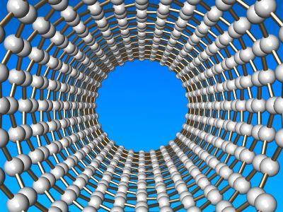
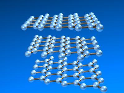
4 Diamond Nanotube Graphite Buckyball
5 Quantum numbers of electrons in a solid The quantum numbers are: Energy E and momentum p = (p x,p y,p z ) They reflect symmetries and thus are conserved (Lect. 6, Slide 12): The energy E is related to translation symmetry in time t. Momentum p is related to translation symmetry in space x = (x,y,z). Translation in time allows t = E = 0 (zero uncertainty in E). Translation in space allows x= p = 0 (zero uncertainty in p). We keep encountering the same four variables: t,x in real space and E,p in reciprocal space Since the quantum numbers E,p live in reciprocal space, one needs to think in reciprocal space when describing solids. As we saw in diffraction (Lect. 9, Slides 11,12), large and small are inverted in reciprocal space.
6 Measuring the quantum numbers of electrons The quantum numbers E and p can be measured by angle-resolved photoemission. This is an elaborate use of the photoelectric effect, which was explained as quantum phenomenon by Einstein : Photon in Electron outside Electron inside Measure E, p of the emitted photoelectron. Subtract E, p of the photon to obtain E, p of the electron inside the solid. Electron energy outside the solid Photon energy = Electron energy inside the solid

7 Momentum p from angle-resolved photoemission p y p x p y p x p y p x
8 The many-particle problem A typical piece of a solid ( cm 3 ) contains electrons (Avogadro s number). How do we deal with all of these electrons? Make = infinity. That actually simplifies the problem, because one can use an infinite crystal and consider only atoms inside one unit cell. With so many electrons the energy levels are very dense and become continuous bands. Solids are good examples demonstrating strange concepts in particle physics, such as antiparticles. These correspond to holes ( = missing electrons ) in semiconductors.
9 Two types of solids To conduct electricity, electrons need to move into an empty level. Metals The energy levels are continuous. Electrons need very little energy to move electrical conductor Energy empty levels filled levels Semiconductors / Insulators Filled and empty energy levels are separated by an energy gap. Electrons need the gap energy to move poor conductor. gap empty levels filled levels
10 Holes = missing electrons Energy electron hole photon A photon with an energy larger than the band gap can move an electron from a filled level to an empty level. The missing electron corresponds to a hole. The missing negative charge gives the hole a positive charge. The result is an electron-hole pair. There is a close analogy in particle physics: Antiparticles are missing particles, like holes. A Gamma photon with 1MeV energy can create an electron-positron pair with a mass of (½+½) MeV/c 2. The vacuum of particle theory is a semiconductor with a 1MeV band gap.
11 Doping of semiconductors To make semiconductors conductive, one introduces extra energy levels by adding a small number of different atoms. Being able to control the conductivity over a wide range by doping makes semiconductors so appealing for electronics. p-type doping Holes in a filled level carry electric current. n-type doping Electrons in an empty level carry electric current. +
12 Light-emitting diode (LED) Energy holes p-doped electrons n-doped + - applied voltage A light-emitting diode combines negative electrons (from a n-doped region) with positive holes (from a p-doped region). An applied voltage pushes the electrons from right to left, where they fill the holes. The energy drop of an electron is converted to a photon. In a LED, electrons fall into holes and emit light.


13 Quantum well laser Energy electrons holes A quantum well laser is an improved LED. Electrons and holes are kept together inside the semiconductor at the center, which has a smaller gap. That makes it easier for electrons to find holes. Alferov Kroemer Nobel Prize in Physics 2000
14 Solar cell A solar cell is an LED in reverse: Photons are absorbed instead of emitted. They generate electrons and holes which are pulled towards front and back contacts. Voltage is generated instead of applied. In a solar cell, a photon creates an electron-hole pair.

15 Energy diagram of a solar cell Energy Electron and hole are pulled in opposite directions by the opposite charges at the n- and p-type doping atoms (Slide 11). It is important to make sure that electrons and holes make it to the contacts without getting trapped or losing energy. Using a single crystal of a semiconductor helps, but is expensive.

16 Transistor + + channel Applying a positive voltage to the gate draws negative electrons into the channel, and thereby closes a switch between source and drain.
17 Semiconductor electronics Semiconductors conduct electricity poorly, but they can be made conducting either by doping (LED, solar cell) or by attracting electrons via a gate voltage (transistor). Computers use silicon transistors,which act as switches. Optoelectronics converts electron-hole pairs to photons and vice versa. Photons are used for long-distance data transfer in fiber-optic cables. LEDs provide energy-efficient and long-lasting lighting. Solar cells produce renewable energy free of pollution.
Classification of Solids
 Classification of Solids Classification by conductivity, which is related to the band structure: (Filled bands are shown dark; D(E) = Density of states) Class Electron Density Density of States D(E) Examples
Semi-Conductors insulators semi-conductors N-type Semi-Conductors P-type Semi-Conductors
 Semi-Conductors In the metal materials considered earlier, the coupling of the atoms together to form the material decouples an electron from each atom setting it free to roam around inside the material.
EE301 Electronics I , Fall
 EE301 Electronics I 2018-2019, Fall 1. Introduction to Microelectronics (1 Week/3 Hrs.) Introduction, Historical Background, Basic Consepts 2. Rewiev of Semiconductors (1 Week/3 Hrs.) Semiconductor materials
From Last Time. Several important conceptual aspects of quantum mechanics Indistinguishability. Symmetry
 From Last Time Several important conceptual aspects of quantum mechanics Indistinguishability particles are absolutely identical Leads to Pauli exclusion principle (one Fermion / quantum state). Symmetry
Lecture 20: Semiconductor Structures Kittel Ch 17, p , extra material in the class notes
 Lecture 20: Semiconductor Structures Kittel Ch 17, p 494-503, 507-511 + extra material in the class notes MOS Structure Layer Structure metal Oxide insulator Semiconductor Semiconductor Large-gap Semiconductor
Electronic Devices & Circuits
 Electronic Devices & Circuits For Electronics & Communication Engineering By www.thegateacademy.com Syllabus Syllabus for Electronic Devices Energy Bands in Intrinsic and Extrinsic Silicon, Carrier Transport,
CHAPTER 11 Semiconductor Theory and Devices
 CHAPTER 11 Semiconductor Theory and Devices 11.1 Band Theory of Solids 11.2 Semiconductor Theory 11.3 Semiconductor Devices 11.4 Nanotechnology It is evident that many years of research by a great many
1 P a g e h t t p s : / / w w w. c i e n o t e s. c o m / Physics (A-level)
") 1 P a g e h t t p s : / / w w w. c i e n o t e s. c o m / Physics (A-level) Electromagnetic induction (Chapter 23): For a straight wire, the induced current or e.m.f. depends on: The magnitude of the magnetic
1 P a g e h t t p s : / / w w w. c i e n o t e s. c o m / Physics (A-level) Electromagnetic induction (Chapter 23): For a straight wire, the induced current or e.m.f. depends on: The magnitude of the magnetic
Lecture 0: Introduction
 Lecture 0: Introduction Introduction q Integrated circuits: many transistors on one chip q Very Large Scale Integration (VLSI): bucketloads! q Complementary Metal Oxide Semiconductor Fast, cheap, low power
Free Electron Model for Metals
 Free Electron Model for Metals Metals are very good at conducting both heat and electricity. A lattice of in a sea of electrons shared between all nuclei (moving freely between them): This is referred
From Last Time Important new Quantum Mechanical Concepts. Atoms and Molecules. Today. Symmetry. Simple molecules.
 Today From Last Time Important new Quantum Mechanical Concepts Indistinguishability: Symmetries of the wavefunction: Symmetric and Antisymmetric Pauli exclusion principle: only one fermion per state Spin
Lecture 20 - Semiconductor Structures
 Lecture 0: Structures Kittel Ch 17, p 494-503, 507-511 + extra material in the class notes MOS Structure metal Layer Structure Physics 460 F 006 Lect 0 1 Outline What is a semiconductor Structure? Created
Chapter Two. Energy Bands and Effective Mass
 Chapter Two Energy Bands and Effective Mass Energy Bands Formation At Low Temperature At Room Temperature Valence Band Insulators Metals Effective Mass Energy-Momentum Diagrams Direct and Indirect Semiconduction
Preview from Notesale.co.uk Page 4 of 35
 field 64 If a dielectric is inserted b/w the plates of a charged capacitor, its Remains Becomes infinite capacitance constant decreases increases 65 Selenium is an insulator in the dark but when exposed
Single Electron Transistor (SET)
") Single Electron Transistor (SET) e - e - dot C g V g A single electron transistor is similar to a normal transistor (below), except 1) the channel is replaced by a small dot. 2) the dot is separated from
Single Electron Transistor (SET) e - e - dot C g V g A single electron transistor is similar to a normal transistor (below), except 1) the channel is replaced by a small dot. 2) the dot is separated from
3C3 Analogue Circuits
 Department of Electronic & Electrical Engineering Trinity College Dublin, 2014 3C3 Analogue Circuits Prof J K Vij jvij@tcd.ie Lecture 1: Introduction/ Semiconductors & Doping 1 Course Outline (subject
EECS143 Microfabrication Technology
 EECS143 Microfabrication Technology Professor Ali Javey Introduction to Materials Lecture 1 Evolution of Devices Yesterday s Transistor (1947) Today s Transistor (2006) Why Semiconductors? Conductors e.g
ESE370: Circuit-Level Modeling, Design, and Optimization for Digital Systems
 ESE370: Circuit-Level Modeling, Design, and Optimization for Digital Systems Lec 6: September 14, 2015 MOS Model You are Here: Transistor Edition! Previously: simple models (0 and 1 st order) " Comfortable
ESE370: Circuit-Level Modeling, Design, and Optimization for Digital Systems. Today MOS MOS. Capacitor. Idea
 ESE370: Circuit-Level Modeling, Design, and Optimization for Digital Systems Day 9: September 26, 2011 MOS Model Today MOS Structure Basic Idea Semiconductor Physics Metals, insulators Silicon lattice
So why is sodium a metal? Tungsten Half-filled 5d band & half-filled 6s band. Insulators. Interaction of metals with light?
 Bonding in Solids: Metals, Insulators, & CHEM 107 T. Hughbanks Delocalized bonding in Solids Think of a pure solid as a single, very large molecule. Use our bonding pictures to try to understand properties.
Bohr s Model, Energy Bands, Electrons and Holes
 Dual Character of Material Particles Experimental physics before 1900 demonstrated that most of the physical phenomena can be explained by Newton's equation of motion of material particles or bodies and
Modern Physics for Frommies IV The Universe - Small to Large Lecture 4
 Fromm Institute for Lifelong Learning University of San Francisco Modern Physics for Frommies IV The Universe - Small to Large Lecture 4 3 February 06 Modern Physics IV Lecture 4 Agenda Administrative
Solid State Physics. Lecture 10 Band Theory. Professor Stephen Sweeney
 Solid State Physics Lecture 10 Band Theory Professor Stephen Sweeney Advanced Technology Institute and Department of Physics University of Surrey, Guildford, GU2 7XH, UK s.sweeney@surrey.ac.uk Recap from
Conductivity and Semi-Conductors
 Conductivity and Semi-Conductors J = current density = I/A E = Electric field intensity = V/l where l is the distance between two points Metals: Semiconductors: Many Polymers and Glasses 1 Electrical Conduction
Engineering 2000 Chapter 8 Semiconductors. ENG2000: R.I. Hornsey Semi: 1
 Engineering 2000 Chapter 8 Semiconductors ENG2000: R.I. Hornsey Semi: 1 Overview We need to know the electrical properties of Si To do this, we must also draw on some of the physical properties and we
EE143 Fall 2016 Microfabrication Technologies. Evolution of Devices
 EE143 Fall 2016 Microfabrication Technologies Prof. Ming C. Wu wu@eecs.berkeley.edu 511 Sutardja Dai Hall (SDH) 1-1 Evolution of Devices Yesterday s Transistor (1947) Today s Transistor (2006) 1-2 1 Why
Current mechanisms Exam January 27, 2012
 Current mechanisms Exam January 27, 2012 There are four mechanisms that typically cause currents to flow: thermionic emission, diffusion, drift, and tunneling. Explain briefly which kind of current mechanisms
Review of Optical Properties of Materials
 Review of Optical Properties of Materials Review of optics Absorption in semiconductors: qualitative discussion Derivation of Optical Absorption Coefficient in Direct Semiconductors Photons When dealing
LESSON 5: ELECTRICITY II
 LESSON 5: ELECTRICITY II The first two points are a review of the previous lesson 1.1.ELECTRIC CHARGE - Electric charge is a property of all objects and is responsible for electrical phenomena. -All matter
Lecture 8. Equations of State, Equilibrium and Einstein Relationships and Generation/Recombination
 Lecture 8 Equations of State, Equilibrium and Einstein Relationships and Generation/Recombination Reading: (Cont d) Notes and Anderson 2 sections 3.4-3.11 Energy Equilibrium Concept Consider a non-uniformly
From nanophysics research labs to cell phones. Dr. András Halbritter Department of Physics associate professor
 From nanophysics research labs to cell phones Dr. András Halbritter Department of Physics associate professor Curriculum Vitae Birth: 1976. High-school graduation: 1994. Master degree: 1999. PhD: 2003.
Single Photon detectors
 Single Photon detectors Outline Motivation for single photon detection Semiconductor; general knowledge and important background Photon detectors: internal and external photoeffect Properties of semiconductor
Free Electron Model for Metals
 Free Electron Model for Metals Metals are very good at conducting both heat and electricity. A lattice of in a sea of electrons shared between all nuclei (moving freely between them): This is referred
Semiconductor Optoelectronics Prof. M. R. Shenoy Department of Physics Indian Institute of Technology, Delhi
 Semiconductor Optoelectronics Prof. M. R. Shenoy Department of Physics Indian Institute of Technology, Delhi Lecture - 1 Context and Scope of the Course (Refer Slide Time: 00:44) Welcome to this course
Designing Information Devices and Systems II A. Sahai, J. Roychowdhury, K. Pister Discussion 1A
 EECS 16B Spring 2019 Designing Information Devices and Systems II A. Sahai, J. Roychowdhury, K. Pister Discussion 1A 1 Semiconductor Physics Generally, semiconductors are crystalline solids bonded into
Lecture Number - 01 Metals, Semiconductors and Insulators
 Electronic Materials, Devices and Fabrication Dr. S. Parasuraman Department of Metallurgical and Materials Engineering Indian Institute of Technology, Madras Lecture Number - 01 Metals, Semiconductors
FREQUENTLY ASKED QUESTIONS February 21, 2017
 FREQUENTLY ASKED QUESTIONS February 21, 2017 Content Questions How do you place a single arsenic atom with the ratio 1 in 100 million? Sounds difficult to get evenly spread throughout. Yes, techniques
1 Review of semiconductor materials and physics
 Part One Devices 1 Review of semiconductor materials and physics 1.1 Executive summary Semiconductor devices are fabricated using specific materials that offer the desired physical properties. There are
Electrons are shared in covalent bonds between atoms of Si. A bound electron has the lowest energy state.
 Photovoltaics Basic Steps the generation of light-generated carriers; the collection of the light-generated carriers to generate a current; the generation of a large voltage across the solar cell; and
Bonding in solids The interaction of electrons in neighboring atoms of a solid serves the very important function of holding the crystal together.
 Bonding in solids The interaction of electrons in neighboring atoms of a solid serves the very important function of holding the crystal together. For example Nacl In the Nacl lattice, each Na atom is
Review of Semiconductor Physics. Lecture 3 4 Dr. Tayab Din Memon
 Review of Semiconductor Physics Lecture 3 4 Dr. Tayab Din Memon 1 Electronic Materials The goal of electronic materials is to generate and control the flow of an electrical current. Electronic materials
CHAPTER 4 RADIATION ATTENUATION
 HDR202 PHYSICS FOR RADIOGRAPHERS 2 CHAPTER 4 RADIATION ATTENUATION PREPARED BY: MR KAMARUL AMIN BIN ABDULLAH SCHOOL OF MEDICAL IMAGING FACULTY OF HEALTH SCIENCES Learning Objectives At the end of the lesson,
EE 446/646 Photovoltaic Devices I. Y. Baghzouz
 EE 446/646 Photovoltaic Devices I Y. Baghzouz What is Photovoltaics? First used in about 1890, the word has two parts: photo, derived from the Greek word for light, volt, relating to electricity pioneer
! Previously: simple models (0 and 1 st order) " Comfortable with basic functions and circuits. ! This week and next (4 lectures)
 Comfortable with basic functions and circuits. ! This week and next (4 lectures)") ESE370: CircuitLevel Modeling, Design, and Optimization for Digital Systems Lec 6: September 14, 2015 MOS Model You are Here: Transistor Edition! Previously: simple models (0 and 1 st order) " Comfortable
ESE370: CircuitLevel Modeling, Design, and Optimization for Digital Systems Lec 6: September 14, 2015 MOS Model You are Here: Transistor Edition! Previously: simple models (0 and 1 st order) " Comfortable
PHYS 3313 Section 001 Lecture #21 Monday, Nov. 26, 2012
 PHYS 3313 Section 001 Lecture #21 Monday, Nov. 26, 2012 Superconductivity Theory, The Cooper Pair Application of Superconductivity Semi-Conductor Nano-technology Graphene 1 Announcements Your presentations
CME 300 Properties of Materials. ANSWERS: Homework 9 November 26, As atoms approach each other in the solid state the quantized energy states:
 CME 300 Properties of Materials ANSWERS: Homework 9 November 26, 2011 As atoms approach each other in the solid state the quantized energy states: are split. This splitting is associated with the wave
The Photoelectric Effect and the Quantization of Light
 The Photoelectric Effect and the Quantization of Light INTRODUCTION When a light with a sufficiently high frequency shines on a metal plate, electrons are ejected from the plate. This effect is known as
Explain how line spectra are produced. In your answer you should describe:
 The diagram below shows the line spectrum of a gas. Explain how line spectra are produced. In your answer you should describe: how the collisions of charged particles with gas atoms can cause the atoms
ESE370: Circuit-Level Modeling, Design, and Optimization for Digital Systems
 ESE370: Circuit-Level Modeling, Design, and Optimization for Digital Systems Lec 6: September 18, 2017 MOS Model You are Here: Transistor Edition! Previously: simple models (0 and 1 st order) " Comfortable
Chapter 38. Photons Light Waves Behaving as Particles
 Chapter 38 Photons Light Waves Behaving as Particles 38.1 The Photoelectric Effect The photoelectric effect was first discovered by Hertz in 1887, and was explained by Einstein in 1905. The photoelectric
The Dielectric Function of a Metal ( Jellium )
") The Dielectric Function of a Metal ( Jellium ) Total reflection Plasma frequency p (10 15 Hz range) Why are Metals Shiny? An electric field cannot exist inside a metal, because metal electrons follow the
The Dielectric Function of a Metal ( Jellium ) Total reflection Plasma frequency p (10 15 Hz range) Why are Metals Shiny? An electric field cannot exist inside a metal, because metal electrons follow the
smal band gap Saturday, April 9, 2011
 small band gap upper (conduction) band empty small gap valence band filled 2s 2p 2s 2p hybrid (s+p)band 2p no gap 2s (depend on the crystallographic orientation) extrinsic semiconductor semi-metal electron
David J. Starling Penn State Hazleton PHYS 214
 Being virtually killed by a virtual laser in a virtual space is just as effective as the real thing, because you are as dead as you think you are. -Douglas Adams, Mostly Harmless David J. Starling Penn
Semiconductor Theory and Devices
 Semiconductor Theory and Devices Band Theory of Solids Semiconductor Theory Semiconductor Devices Nanotechnology It is evident that many years of research by a great many people, both before and after
Sheng S. Li. Semiconductor Physical Electronics. Second Edition. With 230 Figures. 4) Springer
 Springer") Sheng S. Li Semiconductor Physical Electronics Second Edition With 230 Figures 4) Springer Contents Preface 1. Classification of Solids and Crystal Structure 1 1.1 Introduction 1 1.2 The Bravais Lattice
Sheng S. Li Semiconductor Physical Electronics Second Edition With 230 Figures 4) Springer Contents Preface 1. Classification of Solids and Crystal Structure 1 1.1 Introduction 1 1.2 The Bravais Lattice
Single Electron Transistor (SET)
") Single Electron Transistor (SET) SET: e - e - dot A single electron transistor is similar to a normal transistor (below), except 1) the channel is replaced by a small dot. C g 2) the dot is separated from
Single Electron Transistor (SET) SET: e - e - dot A single electron transistor is similar to a normal transistor (below), except 1) the channel is replaced by a small dot. C g 2) the dot is separated from
CARLETON UNIVERSITY. FINAL EXAMINATION December 2016
 CARLETON UNIVERSITY FINAL EXAMINATION December 2016 DURATION: 3 HOURS Department Name & Course Number: Electronics 4705 Course Instructor(s): Tom Smy AUTHORIZED MEMORANDA CALCULATOR (Not Programmable)
Inorganic compounds that semiconduct tend to have an average of 4 valence electrons, and their conductivity may be increased by doping.
 Chapter 12 Modern Materials 12.1 Semiconductors Inorganic compounds that semiconduct tend to have an average of 4 valence electrons, and their conductivity may be increased by doping. Doping yields different
ITT Technical Institute ET215 Devices I Unit 1
 ITT Technical Institute ET215 Devices I Unit 1 Chapter 1 Chapter 2, Sections 2.1-2.4 Chapter 1 Basic Concepts of Analog Circuits Recall ET115 & ET145 Ohms Law I = V/R If voltage across a resistor increases
Fundamentals of Semiconductor Devices Prof. Digbijoy N. Nath Centre for Nano Science and Engineering Indian Institute of Science, Bangalore
 Fundamentals of Semiconductor Devices Prof. Digbijoy N. Nath Centre for Nano Science and Engineering Indian Institute of Science, Bangalore Lecture - 05 Density of states Welcome back. So, today is the
27-1 Planck Solves the Ultraviolet Catastrophe
 27-1 Planck Solves the Ultraviolet Catastrophe By the end of the 19 th century, most physicists were confident that the world was well understood. Aside from a few nagging questions, everything seemed
Joy of Science Discovering the matters and the laws of the universe
 January 16, 2017 Joy of Science Discovering the matters and the laws of the universe Key Words Universe, Energy, Quantum mechanics, Chemical reaction, Structure of matter Unless otherwise noted, all pictures
EA Notes (Scen 101), Tillery Chapter 7. Light
, Tillery Chapter 7. Light") EA Notes (Scen 101), Tillery Chapter 7 Light Introduction Light is hard to study because you can't see it, you only see it's effects. Newton tried to explain the energy in a light beam as the KE of a particle
EA Notes (Scen 101), Tillery Chapter 7 Light Introduction Light is hard to study because you can't see it, you only see it's effects. Newton tried to explain the energy in a light beam as the KE of a particle
PUT YOUR NAME ON THE THIRD PAGE, AND ALL FOLLOWING PAGES
 PUT YOUR NAME ON THE THIRD PAGE, AND ALL FOLLOWING PAGES REFERENCE SHEET FOR CHEM 1 MIDTERM EXAMINATION (Not all data on this sheet will be necessary for any given exam) 1 THIS EXAM HAS 8 PAGES (INCLUDING
Introduction to Sources: Radiative Processes and Population Inversion in Atoms, Molecules, and Semiconductors Atoms and Molecules
 OPTI 500 DEF, Spring 2012, Lecture 2 Introduction to Sources: Radiative Processes and Population Inversion in Atoms, Molecules, and Semiconductors Atoms and Molecules Energy Levels Every atom or molecule
Chapter 4 Scintillation Detectors
 Med Phys 4RA3, 4RB3/6R03 Radioisotopes and Radiation Methodology 4-1 4.1. Basic principle of the scintillator Chapter 4 Scintillation Detectors Scintillator Light sensor Ionizing radiation Light (visible,
ELEMENTARY BAND THEORY
 ELEMENTARY BAND THEORY PHYSICIST Solid state band Valence band, VB Conduction band, CB Fermi energy, E F Bloch orbital, delocalized n-doping p-doping Band gap, E g Direct band gap Indirect band gap Phonon
Semiconductors & LEDs
 Semiconductors & LEDs Day 37, Phys 2130 Questions? Semiconductors &LEDs Next up: EPR, Entanglement, Bell, Bound State Sim.. Many Wells 2 1 In solid, `10 22 atoms/cm 3, many!! electrons, and levels countless
Semiconductors. Semiconductors also can collect and generate photons, so they are important in optoelectronic or photonic applications.
 Semiconductors Semiconducting materials have electrical properties that fall between true conductors, (like metals) which are always highly conducting and insulators (like glass or plastic or common ceramics)
Photodiodes and other semiconductor devices
 Photodiodes and other semiconductor devices Chem 243 Winter 2017 What is a semiconductor? no e - Empty e levels Conduction Band a few e - Empty e levels Filled e levels Filled e levels lots of e - Empty
Unified School District of De Pere Physics Benchmarks
 Content Standards: A. Students will understand that among the science disciplines, there are unifying themes: systems, order, organization, and interactions; evidence, models, and explanations; constancy,
Semiconductors and Optoelectronics. Today Semiconductors Acoustics. Tomorrow Come to CH325 Exercises Tours
 Semiconductors and Optoelectronics Advanced Physics Lab, PHYS 3600 Don Heiman, Northeastern University, 2017 Today Semiconductors Acoustics Tomorrow Come to CH325 Exercises Tours Semiconductors and Optoelectronics
Two-dimensional lattice
 Two-dimensional lattice a 1 *, k x k x =0,k y =0 X M a 2, y Γ X a 2 *, k y a 1, x Reciprocal lattice Γ k x = 0.5 a 1 *, k y =0 k x = 0, k y = 0.5 a 2 * k x =0.5a 1 *, k y =0.5a 2 * X X M k x = 0.25 a 1
Solid State Device Fundamentals
 Solid State Device Fundamentals ENS 345 Lecture Course by Alexander M. Zaitsev alexander.zaitsev@csi.cuny.edu Tel: 718 982 2812 Office 4N101b 1 The free electron model of metals The free electron model
Physics of Semiconductor Devices. Unit 2: Revision of Semiconductor Band Theory
 Physics of Semiconductor Devices Unit : Revision of Semiconductor Band Theory Unit Revision of Semiconductor Band Theory Contents Introduction... 5 Learning outcomes... 5 The Effective Mass... 6 Electrons
sin[( t 2 Home Problem Set #1 Due : September 10 (Wed), 2008
, 2008") Home Problem Set #1 Due : September 10 (Wed), 008 1. Answer the following questions related to the wave-particle duality. (a) When an electron (mass m) is moving with the velocity of υ, what is the wave
Home Problem Set #1 Due : September 10 (Wed), 008 1. Answer the following questions related to the wave-particle duality. (a) When an electron (mass m) is moving with the velocity of υ, what is the wave
Solid State Device Fundamentals
 Solid State Device Fundamentals ENS 345 Lecture Course by Alexander M. Zaitsev alexander.zaitsev@csi.cuny.edu Tel: 718 982 2812 Office 4N101b 1 Outline - Goals of the course. What is electronic device?
Problem Set 10: Solutions
 University of Alabama Department of Physics and Astronomy PH 253 / LeClair Fall 21 Problem Set 1: Solutions 1. For a one-dimensional infinite square well of length l the allowed energies for noninteracting
Lecture 1. OUTLINE Basic Semiconductor Physics. Reading: Chapter 2.1. Semiconductors Intrinsic (undoped) silicon Doping Carrier concentrations
 silicon Doping Carrier concentrations") Lecture 1 OUTLINE Basic Semiconductor Physics Semiconductors Intrinsic (undoped) silicon Doping Carrier concentrations Reading: Chapter 2.1 EE105 Fall 2007 Lecture 1, Slide 1 What is a Semiconductor? Low
Lecture 1 OUTLINE Basic Semiconductor Physics Semiconductors Intrinsic (undoped) silicon Doping Carrier concentrations Reading: Chapter 2.1 EE105 Fall 2007 Lecture 1, Slide 1 What is a Semiconductor? Low
Development and Applications of Acoustic Charge Transport
 Development and Applications of Acoustic Charge Transport CID #478 Physics 222 Term Paper #1 Abstract Acoustic charge transport is accomplished through the use of a surface acoustic wave passing through
Higher Physics. Electricity. Summary Notes. Monitoring and measuring a.c. Current, potential difference, power and resistance
 Higher Physics Electricity Summary Notes Monitoring and measuring a.c. Current, potential difference, power and resistance Electrical sources and internal resistance Capacitors Conductors, semiconductors
Nanoelectronics. Topics
 Nanoelectronics Topics Moore s Law Inorganic nanoelectronic devices Resonant tunneling Quantum dots Single electron transistors Motivation for molecular electronics The review article Overview of Nanoelectronic
For their 1948 discovery of the transistor, John Bardeen, Walter Brattain, and William Shockley were awarded the 1956 Nobel prize in physics.
 Modern Physics (PHY 3305) Lecture Notes Modern Physics (PHY 3305) Lecture Notes Solid-State Physics: Superconductivity (Ch. 10.9) SteveSekula, 1 April 2010 (created 1 April 2010) Review no tags We applied
Experiment objectives: measure the ratio of Planck s constant to the electron charge h/e using the photoelectric effect.
 Chapter 1 Photoelectric Effect Experiment objectives: measure the ratio of Planck s constant to the electron charge h/e using the photoelectric effect. History The photoelectric effect and its understanding
! Previously: simple models (0 and 1 st order) " Comfortable with basic functions and circuits. ! This week and next (4 lectures)
 Comfortable with basic functions and circuits. ! This week and next (4 lectures)") ESE370: CircuitLevel Modeling, Design, and Optimization for Digital Systems Lec 6: September 18, 2017 MOS Model You are Here: Transistor Edition! Previously: simple models (0 and 1 st order) " Comfortable
ESE370: CircuitLevel Modeling, Design, and Optimization for Digital Systems Lec 6: September 18, 2017 MOS Model You are Here: Transistor Edition! Previously: simple models (0 and 1 st order) " Comfortable
3. Two-dimensional systems
 3. Two-dimensional systems Image from IBM-Almaden 1 Introduction Type I: natural layered structures, e.g., graphite (with C nanostructures) Type II: artificial structures, heterojunctions Great technological
1. (a) What is the meaning of semiconductor? [1 mark]
![1. (a) What is the meaning of semiconductor? [1 mark]](/thumbs/75/71650292.jpg "1. (a) What is the meaning of semiconductor? [1 mark]") TRIAL KEDAH 05 ESSAY SECTION B. (a) What is the meaning of semiconductor? [ mark] (b) Diagram 0. shows a boron (B) atom embedded among silicon (Si) atoms in a semiconductor. In Diagram 0. the embedded
TRIAL KEDAH 05 ESSAY SECTION B. (a) What is the meaning of semiconductor? [ mark] (b) Diagram 0. shows a boron (B) atom embedded among silicon (Si) atoms in a semiconductor. In Diagram 0. the embedded
LECTURE 23. MOS transistor. 1 We need a smart switch, i.e., an electronically controlled switch. Lecture Digital Circuits, Logic
 LECTURE 23 Lecture 16-20 Digital Circuits, Logic 1 We need a smart switch, i.e., an electronically controlled switch 2 We need a gain element for example, to make comparators. The device of our dreams
Radiation Detector 2016/17 (SPA6309)
") Radiation Detector 2016/17 (SPA6309) Semiconductor detectors (Leo, Chapter 10) 2017 Teppei Katori Semiconductor detectors are used in many situations, mostly for some kind of high precision measurement.
Radiation Detector 2016/17 (SPA6309) Semiconductor detectors (Leo, Chapter 10) 2017 Teppei Katori Semiconductor detectors are used in many situations, mostly for some kind of high precision measurement.
Acoustics and Fourier Transform
 AFT Acoustics and Fourier Transform 1. A Hamming filter is used to compute FFT (Fast Fourier Transform) plots in the AFT experiment. What is the reason for using such a filter? 2. Briefly describe what
GAMMA RAY SPECTROSCOPY
 GAMMA RAY SPECTROSCOPY Gamma Ray Spectroscopy 1 In this experiment you will use a sodium iodide (NaI) detector along with a multichannel analyzer (MCA) to measure gamma ray energies from energy level transitions
Essentials of Quantum Physics
 Essentials of Quantum Physics References Direct energy conversion by S.W. Angrist, Ch 3. (out of print text book) Essential Quantum Physics by Peter Landshoff, Allen Metherell and Gareth Rees, 1997, Cambridge
Photoelectron Spectroscopy
 Stefan Hüfner Photoelectron Spectroscopy Principles and Applications Third Revised and Enlarged Edition With 461 Figures and 28 Tables JSJ Springer ... 1. Introduction and Basic Principles 1 1.1 Historical
Chapter 9: Quantization of Light
 Chapter 9: Quantization of Light Max Planck started the revolution of quantum theory by challenging the classical physics and the classical wave theory of light. He proposed the concept of quantization
PHOTOVOLTAICS Fundamentals
 PHOTOVOLTAICS Fundamentals PV FUNDAMENTALS Semiconductor basics pn junction Solar cell operation Design of silicon solar cell SEMICONDUCTOR BASICS Allowed energy bands Valence and conduction band Fermi
Chem 481 Lecture Material 3/20/09
 Chem 481 Lecture Material 3/20/09 Radiation Detection and Measurement Semiconductor Detectors The electrons in a sample of silicon are each bound to specific silicon atoms (occupy the valence band). If
Floating Point Representation and Digital Logic. Lecture 11 CS301
 Floating Point Representation and Digital Logic Lecture 11 CS301 Administrative Daily Review of today s lecture w Due tomorrow (10/4) at 8am Lab #3 due Friday (9/7) 1:29pm HW #5 assigned w Due Monday 10/8
ELECTRONIC DEVICES AND CIRCUITS SUMMARY
 ELECTRONIC DEVICES AND CIRCUITS SUMMARY Classification of Materials: Insulator: An insulator is a material that offers a very low level (or negligible) of conductivity when voltage is applied. Eg: Paper,
Wavelength of 1 ev electron
 HW8: M Chap 15: Question B, Exercises 2, 6 M Chap 16: Question B, Exercises 1 M Chap 17: Questions C, D From Last Time Essay topic and paragraph due Friday, Mar. 24 Light waves are particles and matter
CCD OPERATION. The BBD was an analog delay line, made up of capacitors such that an analog signal was moving along one step at each clock cycle.
 CCDS Lesson 4 CCD OPERATION The predecessor of the CCD was a device called the BUCKET BRIGADE DEVICE developed at the Phillips Research Labs The BBD was an analog delay line, made up of capacitors such