Characterization of Irradiated Doping Profiles. Wolfgang Treberspurg, Thomas Bergauer, Marko Dragicevic, Manfred Krammer, Manfred Valentan
|
|
|
- Daniella York
- 6 years ago
- Views:
Transcription
1 Characterization of Irradiated Doping Profiles, Thomas Bergauer, Marko Dragicevic, Manfred Krammer, Manfred Valentan Vienna Conference on Instrumentation (VCI)
2 Content: Experimental Procedure Sample Irradiation Spreading Resistance Profiling (SRP) Theoretical Background The Electrical Neutral Bulk (ENB) The Space Charge Region (SCR) Results Irradiated Profiles of Shallow Impurities Effective Doping Concentration References
3 3 Experimental Procedure

4 4 Experimental Procedure: Irradiation Samples: Floating-zone, p-on-n diodes 1 kωcm bulk resistivity Produced by HPK Bulk and backside implant doped with phosphor Overview: Sample irradiation Annealing of 8 minutes at 60 C Mechanically cut Preparation for SRP measurements Common capacitance voltage measurements Sample Selection Irradiation and Annealing SRP Measurements CV Measurements
 Vienna Previous fluence calibration with similar diodes 27 C during irradiation place Spectrum")
5 5 Experimental Procedure: Irradiation Irradiation facility: TRIGA Mark-II nuclear reactor At the Institute of Atomic and Subatomic Physics (ATI) Vienna Previous fluence calibration with similar diodes 27 C during irradiation place Spectrum approximately known
6 6 Experimental Procedure: Irradiation Calculation: Hardness factor κ has been measured during calibration Calculation of κ confirmed calibration results Damage mainly caused by thermal and fast neutrons D( E) ( E) de D(1MeV ) ( E) de V I Sample Φ eq [n eq /cm 2 ]

 The resistance is measured at each position 16.07.")
7 Experimental Procedure: SRP Preparation: The samples are mechanically grinded and polished with a small bevel angle During preparation no temperatures above 30 C are expected Measurement: Two closely aligned probes are stepped along the beveled surface The probes are contacted with reproducible weight The probes are made of hard material (tungsten carbide) The resistance is measured at each position
 SRP measurements deliver no absolute data, the accuracy depends on the calibration effort Only electrically")
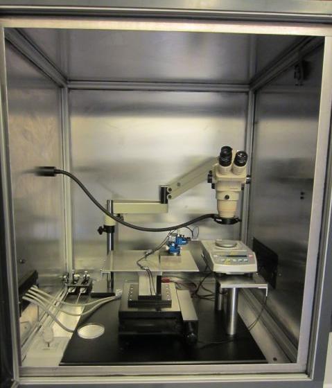
8 8 Experimental Procedure: SRP Data Extraction: The measured resistance is dominated by current spreading effects (R sp ) Very small radii (a) of the probe tips result in a high sensitivity on the material resistivity Depth resolution of about 100 nm can be easily achieved (10 µm planar) SRP measurements deliver no absolute data, the accuracy depends on the calibration effort Only electrically active dopants contribute to the measurement Performance: The measurements have been done in a custom designed setup [1] R sp 2a ( x) ( qn( x) ) 1
9 9 Theoretical Background
10 10 Theoretical Background: ENB The electrical neutral bulk Non depleted silicon volume At sensor operated with voltages smaller than the full depletion voltage The ionization of traps is determined by the Fermi level occupancy function at equilibrium Suited for direct resistivity measurements Modelling of resistivity The shift of the fermi level (E F ) after irradiation is determined by the charge neutrality equation Ionization of acceptor N a - and donor traps N d + has to be taken into account The resistivity is determined by concentration of free charge carrier inside the ENB (n,p) Models have to assumed the number and energy level of traps [2,3] SCR ENB n N a p N d
11 11 Theoretical Background: SCR The space charge region Inside the SCR the ionization of deep traps is regulated by band bending in respect to the potential distribution Almost all deep traps contribute to the effective doping concentration N eff Donor removal processes Vacancies or self interstitials remove dopants from regular sides Donor removal takes place until a non removable amount of donors is reached, which depends on the presence of other elements inside the bulk [4] In turn the donor removal constant c also depends on the initial concentration N eff,0
12 12 Theoretical Background: SCR Capacitance measurements at the presents of deep traps Deep trap usually only contribute at low frequencies, in respect to their time constant As the dc bias voltage correlates to very small frequencies most traps inside the SCR (X Trap ) are ionized Only traps inside the volume dx Ampl which is depleted by the ac test signal are sensitive on the measurement frequency [5] Example The contribution to capacitance measurements of one deep donor like trap is shown Strong influence of measurement parameters: Frequency (responding traps) Amplitude (sensitive volume) Temperature (time constant changes with T) Measurement mode (serial or parallel)
13 13 Measurement Results
14 14 Results: Shallow Impurities Profiles after irradiation Due to donor removal the expected resistivity decrease is observed The donor removal process results in an decreasing implantation depth for increasing fluences Explanation Uniformly distributed defects are expected to shift the profile only Shifting a profile results in a linear correlation of the initial concentration to the resulting one Effect can be understood by assuming that the resulting bulk concentrations converges to the non removable donor concentration Another approach is to assume spatial effects due to high resistivity gradients
15 15 Results: Shallow Impurities Annealing study To investigate a possible influence of annealing on this effect several subsequent annealing steps have been performed (0, 8, 28, 120 minutes at 60 C) No further changes of profiles could be observed, the effect has to take place during irradiation Only shallow impurities are measured, especially after high fluences the electrical behaviour is dominated by deep traps
16 16 Results: Effective Doping Concentration Electrical behaviour The influence of the observed effect on the electrical performance is studied by using capacitance voltage measurements Samples irradiated with more than last ones type inverted n eq /cm 2 have been observed to be type inverted Capacitance measurements become strongly frequency dependent, which make it advisable to use capacitance voltage frequency surfaces C-V Measurement: Parallel mode, -15 C, Amplitude: 200mV, Frequency: 1k


17 Results: Effective Doping Concentration 1E11 5E11 2E12 3E12 1E13 5E13 1E14 5E14 C-V Measurements on diodes irradiated with increasing fluencies: Parallel mode, -15 C Amplitude: 200mV
18 18 Results: Effective Doping Concentration Electrical behaviour The influence of the observed effect on the electrical performance is studied with capacitance voltage measurements Type inverted samples feature a peak at low frequencies due to dominant deep traps The capacitance stabilize at high frequencies for all samples at a value associated with the geometrical capacitance [6] High fluences result in an decreasing dependence on the bias voltage C-V Measurement: Parallel mode, -15 C, Amplitude: 200mV, Frequency: 1k, Bias Voltage: 50V
19 19 Results: Effective Doping Concentration Doping profiles of N eff By differentiating C -2 a profile of the effective doping concentration inside the SCR is calculated [7] At the presented low fluence range donor removal effects are dominant and the concentration decreases With increasing fluences the profiles become inhomogeneous, especially close to the backside, where donor removal mainly takes place C-V Measurement: Parallel mode, - 15 C, Amplitude: 200mV, Frequency: 1k
20 20 Conclusion and Outlook Conclusions It could be shown, that SRP measurements are suited to characterize profiles of shallow donors after irradiation An effect of decreasing implantation depth of shallow impurities with increasing fluences could be observed To evaluate the influence of this effect on the sensor performance capacitance voltage measurements are suited Outlook Capacitance voltage measurements have to be investigated in future and may serve for more detailed impurity characterization The measurement of shallow impurities only with high spatial resolution may be used for investigating their correlation to other impurities
21 21 References [1] W. Treberspurg et al., Measuring Doping Profiles of Silicon Detectors with a Custom-designed Probe Station, Journal of Instrumentation 7 (2012). /doi: / /7/11/p11009 [2] E. Borchi et al., Radiation Damage in Silicon Detectors, La Rivista del Nuovo Cimento, vol. 17, (1994) p [3] M. Bruzzi, Radiation Damage in Silicon Detectors for High-Energy Physics Experiments, IEEE Transactions on nuclear science 48/4 (2001) 960. /doi: / [4] M. Moll et al., Investigation on the improved radiation hardness of silicon detectors with high oxygen concentration, Nucl. Instr. and Meth. A 439 (2000). /doi: /s (99) [5] W. Dabrowski et al., Effects of deep imperfection levels on the capacitance of semiconductor Detectors, Nucl. Instr. and Meth. A 276 (1989). [6] Z. Li et al., Studies of Frequency Dependent C-V Characteristics of Neutron Irradiated p-n Silicon Detectors, IEEE Transactions on nuclear science, Vol. 38, No. 2, (1991) [8] j. Shiau et al., Interpretation of capacitance versus voltage measurements in the presence of a high density of deep levels, J. Appl. Phys. 59, 2879 (1986); doi: /
Silicon Detectors in High Energy Physics
 Thomas Bergauer (HEPHY Vienna) IPM Teheran 22 May 2011 Sunday: Schedule Semiconductor Basics (45 ) Silicon Detectors in Detector concepts: Pixels and Strips (45 ) Coffee Break Strip Detector Performance
EUROPEAN ORGANIZATION FOR NUCLEAR RESEARCH STUDIES OF THE RADIATION HARDNESS OF OXYGEN-ENRICHED SILICON DETECTORS
 EUROPEAN ORGANIZATION FOR NUCLEAR RESEARCH CERN EP/98 62 11 Juin 1998 STUDIES OF THE RADIATION HARDNESS OF OXYGEN-ENRICHED SILICON DETECTORS A. Ruzin, G. Casse 1), M. Glaser, F. Lemeilleur CERN, Geneva,
Charge Collection and Capacitance-Voltage analysis in irradiated n-type magnetic Czochralski silicon detectors
 Charge Collection and Capacitance-Voltage analysis in irradiated n-type magnetic Czochralski silicon detectors M. K. Petterson, H.F.-W. Sadrozinski, C. Betancourt SCIPP UC Santa Cruz, 1156 High Street,
Semiconductor Physics fall 2012 problems
 Semiconductor Physics fall 2012 problems 1. An n-type sample of silicon has a uniform density N D = 10 16 atoms cm -3 of arsenic, and a p-type silicon sample has N A = 10 15 atoms cm -3 of boron. For each
Mara Bruzzi INFN and University of Florence, Italy and SCIPP, UC Santa Cruz, USA
 SCIPP 06/16 September 2006 Capacitance-Voltage analysis at different temperatures in heavily irradiated silicon detectors Mara Bruzzi INFN and University of Florence, Italy and SCIPP, UC Santa Cruz, USA
The annealing of interstitial carbon atoms in high resistivity n-type silicon after proton irradiation
 ROSE/TN/2002-01 The annealing of interstitial carbon atoms in high resistivity n-type silicon after proton irradiation M. Kuhnke a,, E. Fretwurst b, G. Lindstroem b a Department of Electronic and Computer
Modeling of charge collection efficiency degradation in semiconductor devices induced by MeV ion beam irradiation
 Modeling of charge collection efficiency degradation in semiconductor devices induced by MeV ion beam irradiation Ettore Vittone Physics Department University of Torino - Italy 1 IAEA Coordinate Research
Development of Radiation Hard Si Detectors
 Development of Radiation Hard Si Detectors Dr. Ajay K. Srivastava On behalf of Detector Laboratory of the Institute for Experimental Physics University of Hamburg, D-22761, Germany. Ajay K. Srivastava
SURVEY OF RECENT RADIATION DAMGE STUDIES AT HAMBURG
 SURVEY OF RECENT RADIATION DAMGE STUDIES AT HAMBURG E. Fretwurst 1, D. Contarato 1, F. Hönniger 1, G. Kramberger 2 G. Lindström 1, I. Pintilie 1,3, A. Schramm 1, J. Stahl 1 1 Institute for Experimental
Correction of the electric resistivity distribution of Si wafers using selective neutron transmutation doping (SNTD) in MARIA nuclear research reactor
 in MARIA nuclear research reactor") NUKLEONIKA 2012;57(3):363 367 ORIGINAL PAPER Correction of the electric resistivity distribution of Si wafers using selective neutron transmutation doping (SNTD) in MARIA nuclear research reactor Mikołaj
NUKLEONIKA 2012;57(3):363 367 ORIGINAL PAPER Correction of the electric resistivity distribution of Si wafers using selective neutron transmutation doping (SNTD) in MARIA nuclear research reactor Mikołaj
Radiation Damage in Silicon Detectors for High-Energy Physics Experiments
 960 IEEE TRANSACTIONS ON NUCLEAR SCIENCE, VOL. 48, NO. 4, AUGUST 2001 Radiation Damage in Silicon Detectors for High-Energy Physics Experiments Mara Bruzzi Abstract Radiation effects in silicon detectors
Joint ICTP-IAEA Workshop on Physics of Radiation Effect and its Simulation for Non-Metallic Condensed Matter.
 2359-3 Joint ICTP-IAEA Workshop on Physics of Radiation Effect and its Simulation for Non-Metallic Condensed Matter 13-24 August 2012 Electrically active defects in semiconductors induced by radiation
Tracking Detector Material Issues for the slhc
 Tracking Detector Material Issues for the slhc Hartmut F.-W. Sadrozinski SCIPP, UC Santa Cruz, CA 95064 Hartmut F.-W. Sadrozinski, US ATLAS Upgrade Meeting Nov 10, 2005 1 Outline of the talk - Motivation
Radiation hardness of Low Gain Amplification Detectors (LGAD)
") Radiation hardness of Low Gain Amplification Detectors (LGAD) G. Kramberger, V. Cindro, I. Mandić, M. Mikuž Ϯ, M. Zavrtanik Jožef Stefan Institute, Ljubljana, Slovenia Ϯ also University of Ljubljana, Faculty
Radiation hardness of Low Gain Amplification Detectors (LGAD) G. Kramberger, V. Cindro, I. Mandić, M. Mikuž Ϯ, M. Zavrtanik Jožef Stefan Institute, Ljubljana, Slovenia Ϯ also University of Ljubljana, Faculty
RD50 Recent Results - Development of radiation hard sensors for SLHC
 - Development of radiation hard sensors for SLHC Anna Macchiolo Max-Planck-Institut für Physik Föhringer Ring 6, Munich, Germany E-mail: Anna.Macchiolo@mppmu.mpg.de on behalf of the RD50 Collaboration
Session 6: Solid State Physics. Diode
 Session 6: Solid State Physics Diode 1 Outline A B C D E F G H I J 2 Definitions / Assumptions Homojunction: the junction is between two regions of the same material Heterojunction: the junction is between
Semiconductor-Detectors
 Semiconductor-Detectors 1 Motivation ~ 195: Discovery that pn-- junctions can be used to detect particles. Semiconductor detectors used for energy measurements ( Germanium) Since ~ 3 years: Semiconductor
Review Energy Bands Carrier Density & Mobility Carrier Transport Generation and Recombination
 Review Energy Bands Carrier Density & Mobility Carrier Transport Generation and Recombination The Metal-Semiconductor Junction: Review Energy band diagram of the metal and the semiconductor before (a)
KATIHAL FİZİĞİ MNT-510
 KATIHAL FİZİĞİ MNT-510 YARIİLETKENLER Kaynaklar: Katıhal Fiziği, Prof. Dr. Mustafa Dikici, Seçkin Yayıncılık Katıhal Fiziği, Şakir Aydoğan, Nobel Yayıncılık, Physics for Computer Science Students: With
Radiation Damage in Silicon Detectors - An introduction for non-specialists -
 CERN EP-TA1-SD Seminar 14.2.2001 Radiation Damage in Silicon Detectors - An introduction for non-specialists - Michael Moll CERN EP - Geneva ROSE Collaboration (CERN RD48) ROSE - Research and Development
Final Examination EE 130 December 16, 1997 Time allotted: 180 minutes
 Final Examination EE 130 December 16, 1997 Time allotted: 180 minutes Problem 1: Semiconductor Fundamentals [30 points] A uniformly doped silicon sample of length 100µm and cross-sectional area 100µm 2
Radiation Damage In Silicon Detectors
 UNIVERZA V LJUBLJANI FAKULTETA ZA MATEMATIKO IN FIZIKO ODDELEK ZA FIZIKO Joµzef Pulko SEMINAR Radiation Damage In Silicon Detectors MENTOR: prof. dr. Vladimir Cindro Abstract: Radiation damage in silicon
Silicon Detectors in High Energy Physics
 Thomas Bergauer (HEPHY Vienna) IPM Teheran 22 May 2011 Sunday: Schedule Silicon Detectors in Semiconductor Basics (45 ) Detector concepts: Pixels and Strips (45 ) Coffee Break Strip Detector Performance
A new protocol to evaluate the charge collection efficiency degradation in semiconductor devices induced by MeV ions
 Session 12: Modification and Damage: Contribute lecture O-35 A new protocol to evaluate the charge collection efficiency degradation in semiconductor devices induced by MeV ions Ettore Vittone Physics
CMS Note Mailing address: CMS CERN, CH-1211 GENEVA 23, Switzerland
 Available on CMS information server CMS NOTE 2001/023 The Compact Muon Solenoid Experiment CMS Note Mailing address: CMS CERN, CH-1211 GENEVA 23, Switzerland May 18, 2001 Investigations of operating scenarios
RADIATION HARDNESS OF SILICON DETECTORS FOR APPLICATIONS IN HIGH-ENERGY PHYSICS EXPERIMENTS. E. Fretwurst, M. Kuhnke, G. Lindström, M.
 Journal of Optoerlectronics and Advanced Mateials Vol. 2, No. 5, 2, p. 575-588 Section 4: Semiconductors RADIATION HARDNESS OF SILICON DETECTORS FOR APPLICATIONS IN HIGH-ENERGY PHYSICS EXPERIMENTS E. Fretwurst,
Leakage current of hadron irradiated silicon detectors - material dependence. ROSE/CERN-RD48 collaboration
 Paper submitted to the 2 nd International Conference on Radiation Effects on Semiconductor Materials, Detectors and Devices, held at the Grand Hotel Mediterraneo, Firenze, Italy, March 4-6, 1998, to be
A double junction model of irradiated silicon pixel sensors for LHC
 Physics Physics Research Publications Purdue University Year 2006 A double junction model of irradiated silicon pixel sensors for LHC V. Chiochia, M. Swartz, Y. Allkofer, D. Bortoletto, L. Cremaldi, S.
Lecture 2. Introduction to semiconductors Structures and characteristics in semiconductors
 Lecture 2 Introduction to semiconductors Structures and characteristics in semiconductors Semiconductor p-n junction Metal Oxide Silicon structure Semiconductor contact Literature Glen F. Knoll, Radiation
Diodes. anode. cathode. cut-off. Can be approximated by a piecewise-linear-like characteristic. Lecture 9-1
 Diodes mplest nonlinear circuit element Basic operation sets the foundation for Bipolar Junction Transistors (BJTs) Also present in Field Effect Transistors (FETs) Ideal diode characteristic anode cathode
physics/ Sep 1997
 GLAS-PPE/97-6 28 August 1997 Department of Physics & Astronomy Experimental Particle Physics Group Kelvin Building, University of Glasgow, Glasgow, G12 8QQ, Scotland. Telephone: +44 - ()141 3398855 Fax:
arxiv:physics/ v2 [physics.ins-det] 18 Jul 2000
![arxiv:physics/ v2 [physics.ins-det] 18 Jul 2000](/thumbs/86/94459867.jpg "arxiv:physics/ v2 [physics.ins-det] 18 Jul 2000") Lorentz angle measurements in irradiated silicon detectors between 77 K and 3 K arxiv:physics/759v2 [physics.ins-det] 18 Jul 2 W. de Boer a, V. Bartsch a, J. Bol a, A. Dierlamm a, E. Grigoriev a, F. Hauler
Lorentz angle measurements in irradiated silicon detectors between 77 K and 3 K arxiv:physics/759v2 [physics.ins-det] 18 Jul 2 W. de Boer a, V. Bartsch a, J. Bol a, A. Dierlamm a, E. Grigoriev a, F. Hauler
MOS CAPACITOR AND MOSFET
 EE336 Semiconductor Devices 1 MOS CAPACITOR AND MOSFET Dr. Mohammed M. Farag Ideal MOS Capacitor Semiconductor Devices Physics and Technology Chapter 5 EE336 Semiconductor Devices 2 MOS Capacitor Structure
Simulation results from double-sided and standard 3D detectors
 Simulation results from double-sided and standard 3D detectors David Pennicard, University of Glasgow Celeste Fleta, Chris Parkes, Richard Bates University of Glasgow G. Pellegrini, M. Lozano - CNM, Barcelona
Ranjeet Dalal, Ashutosh Bhardwaj, Kirti Ranjan, Kavita Lalwani and Geetika Jain
 Simulation of Irradiated Si Detectors, Ashutosh Bhardwaj, Kirti Ranjan, Kavita Lalwani and Geetika Jain CDRST, Department of physics and Astrophysics, University of Delhi, India E-mail: rdalal@cern.ch
Semiconductor Detectors
 Semiconductor Detectors Summary of Last Lecture Band structure in Solids: Conduction band Conduction band thermal conductivity: E g > 5 ev Valence band Insulator Charge carrier in conductor: e - Charge
Hussein Ayedh. PhD Studet Department of Physics
 Hussein Ayedh PhD Studet Department of Physics OUTLINE Introduction Semiconductors Basics DLTS Theory DLTS Requirements Example Summary Introduction Energetically "deep trapping levels in semiconductor
Semiconductor Physics fall 2012 problems
 Semiconductor Physics fall 2012 problems 1. An n-type sample of silicon has a uniform density N D = 10 16 atoms cm -3 of arsenic, and a p-type silicon sample has N A = 10 15 atoms cm -3 of boron. For each
PICTS Analysis of Extended Defects in Heavily Irradiated Silicon
 IEEE TRANSACTIONS ON NUCLEAR SCIENCE, VOL. 49, NO. 5, OCTOBER 2002 2431 PICTS Analysis of Extended Defects in Heavily Irradiated Silicon David Menichelli, Emilio Borchi, Zheng Li, and Mara Bruzzi Abstract
Numerical Modelling of Si sensors for HEP experiments and XFEL
 Numerical Modelling of Si sensors for HEP experiments and XFEL Ajay K. Srivastava 1, D. Eckstein, E. Fretwurst, R. Klanner, G. Steinbrück Institute for Experimental Physics, University of Hamburg, D-22761
Midterm I - Solutions
 UNIVERSITY OF CALIFORNIA College of Engineering Department of Electrical Engineering and Computer Sciences EECS 130 Spring 2008 Professor Chenming Hu Midterm I - Solutions Name: SID: Grad/Undergrad: Closed
arxiv: v1 [physics.ins-det] 25 May 2017
![arxiv: v1 [physics.ins-det] 25 May 2017](/thumbs/93/111674203.jpg "arxiv: v1 [physics.ins-det] 25 May 2017") physica status solidi Description of radiation damage in diamond sensors using an effective defect model Florian Kassel *,1,2, Moritz Guthoff 2, Anne Dabrowski 2, Wim de Boer 1 1 Institute for Experimental
physica status solidi Description of radiation damage in diamond sensors using an effective defect model Florian Kassel *,1,2, Moritz Guthoff 2, Anne Dabrowski 2, Wim de Boer 1 1 Institute for Experimental
Measurement of the acceptor removal rate in silicon pad diodes
 Measurement of the acceptor removal rate in silicon pad diodes P. Dias de Almeida a,b, I. Mateu a,c, M. Fernández Garcia d, M. Moll a a CERN b Fundação para a Ciência e a Tecnologia (FCT) c Centro de Investigaciones
Control of the fabrication process for the sensors of the CMS Silicon Strip Tracker. Anna Macchiolo. CMS Collaboration
 Control of the fabrication process for the sensors of the CMS Silicon Strip Tracker Anna Macchiolo Universita di Firenze- INFN Firenze on behalf of the CMS Collaboration 6 th International Conference on
Effective masses in semiconductors
 Effective masses in semiconductors The effective mass is defined as: In a solid, the electron (hole) effective mass represents how electrons move in an applied field. The effective mass reflects the inverse
UNIVERSITY of CALIFORNIA SANTA CRUZ
 UNIVERSITY of CALIFORNIA SANTA CRUZ EXTRACTION OF EFFECTIVE DOPING CONCENTRATIONS IN UN-IRRADIATED AND IRRADIATED SILICON DETECTORS A thesis submitted in partial satisfaction of the requirements for the
Section 12: Intro to Devices
 Section 12: Intro to Devices Extensive reading materials on reserve, including Robert F. Pierret, Semiconductor Device Fundamentals EE143 Ali Javey Bond Model of Electrons and Holes Si Si Si Si Si Si Si
characterization in solids
 Electrical methods for the defect characterization in solids 1. Electrical residual resistivity in metals 2. Hall effect in semiconductors 3. Deep Level Transient Spectroscopy - DLTS Electrical conductivity
X-ray Radiation Damage in P-N Junction Diode
 X-ray Radiation Damage in P-N Junction Diode Itsara Srithanachai 1, Surada Ueamanapong 1, Yuwadee Sundarasaradula 1, Amporn Poyai 2, Surasak Niemcharoen 1 1 Department of Electronics, Faculty of Engineering,
ATL-INDET /04/2000
 Evolution of silicon micro-strip detector currents during proton irradiation at the CERN PS ATL-INDET-2000-009 17/04/2000 R.S.Harper aλ, P.P.Allport b, L.Andricek c, C.M.Buttar a, J.R.Carter d, G.Casse
Development of radiation hard sensors for very high luminosity colliders - CERN - RD50 project -
 NIMA 1 NIMA RD5 Internal Note - RD5/23/1 Reviewed manuscript submitted to Vertex 22 Development of radiation hard sensors for very high luminosity colliders - CERN - RD5 project - Michael Moll * CERN,
Semiconductor Detectors are Ionization Chambers. Detection volume with electric field Energy deposited positive and negative charge pairs
 1 V. Semiconductor Detectors V.1. Principles Semiconductor Detectors are Ionization Chambers Detection volume with electric field Energy deposited positive and negative charge pairs Charges move in field
GaN for use in harsh radiation environments
 4 th RD50 - Workshop on radiation hard semiconductor devices for very high luminosity colliders GaN for use in harsh radiation environments a (W Cunningham a, J Grant a, M Rahman a, E Gaubas b, J Vaitkus
Creation and annealing of point defects in germanium crystal lattices by subthreshold energy events
 Creation and annealing of point defects in germanium crystal lattices by subthreshold energy events University of Sevilla 203 Sergio M. M. Coelho, Juan F. R. Archilla 2 and F. Danie Auret Physics Department,
Components of a generic collider detector
 Lecture 24 Components of a generic collider detector electrons - ionization + bremsstrahlung photons - pair production in high Z material charged hadrons - ionization + shower of secondary interactions
Tracking in High Energy Physics: Silicon Devices!
 Tracking in High Energy Physics: Silicon Devices! G. Leibenguth XIX Graduiertenkolleg Heidelberg 11-12. October 2007 Content Part 1: Basics on semi-conductor Part 2: Construction Part 3: Two Examples Part
Lecture 2. Introduction to semiconductors Structures and characteristics in semiconductors
 Lecture 2 Introduction to semiconductors Structures and characteristics in semiconductors Semiconductor p-n junction Metal Oxide Silicon structure Semiconductor contact Literature Glen F. Knoll, Radiation
Chapter 7. The pn Junction
 Chapter 7 The pn Junction Chapter 7 PN Junction PN junction can be fabricated by implanting or diffusing donors into a P-type substrate such that a layer of semiconductor is converted into N type. Converting
Electrically active defects in semiconductors induced by radiation
 Electrically active defects in semiconductors induced by radiation Ivana Capan Rudjer Boskovic Institute, Croatia http://www.irb.hr/users/capan Outline Radiation damage Capacitance transient techniques
2. Point Defects. R. Krause-Rehberg
 R. Krause-Rehberg 2. Point Defects (F-center in NaCl) 2.1 Introduction 2.2 Classification 2.3 Notation 2.4 Examples 2.5 Peculiarities in Semiconductors 2.6 Determination of Structure and Concentration
Radiation damage models: comparison between Silvaco and Synopsys
 Radiation damage models: comparison between Silvaco and Synopsys J. Beyer a), M. Bomben b), A. Macchiolo a), R. Nisius a) a) Max Planck Institut für Physik, München b) LPNHE & Université Paris Diderot,
Introduction. Neutron Effects NSEU. Neutron Testing Basics User Requirements Conclusions
 Introduction Neutron Effects Displacement Damage NSEU Total Ionizing Dose Neutron Testing Basics User Requirements Conclusions 1 Neutron Effects: Displacement Damage Neutrons lose their energy in semiconducting
D DAVID PUBLISHING. Transport Properties of InAs-InP Solid Solutions. 2. Experiment. 1. Introduction. 3. Results and Discussion
 Journal of Electrical Engineering 2 (2014) 207-212 doi: 10.17265/2328-2223/2014.05.002 D DAVID PUBLISHING Nodar Kekelidze 1, 2, 3, Elza Khutsishvili 1, 2, Bella Kvirkvelia 1, 2, 3, David Kekelidze 2, Vugar
Semiconductor Physics. Lecture 6
 Semiconductor Physics Lecture 6 Recap pn junction and the depletion region Driven by the need to have no gradient in the fermi level free carriers migrate across the pn junction leaving a region with few
Carriers Concentration in Semiconductors - V. Prof.P. Ravindran, Department of Physics, Central University of Tamil Nadu, India
 Carriers Concentration in Semiconductors - V 1 Prof.P. Ravindran, Department of Physics, Central University of Tamil Nadu, India http://folk.uio.no/ravi/semi2013 Motion and Recombination of Electrons and
Chap. 11 Semiconductor Diodes
 Chap. 11 Semiconductor Diodes Semiconductor diodes provide the best resolution for energy measurements, silicon based devices are generally used for charged-particles, germanium for photons. Scintillators
Semiconductor Physics Problems 2015
 Semiconductor Physics Problems 2015 Page and figure numbers refer to Semiconductor Devices Physics and Technology, 3rd edition, by SM Sze and M-K Lee 1. The purest semiconductor crystals it is possible
Semi-insulating SiC substrates for high frequency devices
 Klausurtagung Silberbach, 19. - 21. Feb. 2002 Institut für Werkstoffwissenschaften - WW 6 Semi-insulating SiC substrates for high frequency devices Vortrag von Matthias Bickermann Semi-insulating SiC substrates
CMS Note Mailing address: CMS CERN, CH-1211 GENEVA 23, Switzerland
 Available on CMS information server CMS NOTE 199/11 The Compact Muon Solenoid Experiment CMS Note Mailing address: CMS CERN, CH-1211 GENEVA 23, Switzerland 11 February 199 Temperature dependence of the
Study of radiation damage induced by 82 MeV protons on multipixel Geiger-mode avalanche photodiodes
 Study of radiation damage induced by 82 MeV protons on multipixel Geiger-mode avalanche photodiodes Y. Musienko*, S. Reucroft, J. Swain (Northeastern University, Boston) D. Renker, K. Dieters (PSI, Villigen)
Characterization of Semiconductors by Capacitance Methods
 University of Iceland 30th April 2007 Experimental physics Characterization of Semiconductors by Capacitance Methods Líney Halla Kristinsdóttir Pétur Gordon Hermannsson Sigurður Ægir Jónsson Instructor:
A study of the double-acceptor level of the silicon divacancy in a proton irradiated n-channel CCD.
 A study of the double-acceptor level of the silicon divacancy in a proton irradiated n-channel CCD. D. Wood*, D. Hall, J.P.D Gow and A. Holland. Centre for Electronic Imaging, The Open University, Milton
Lecture 04 Review of MOSFET
 ECE 541/ME 541 Microelectronic Fabrication Techniques Lecture 04 Review of MOSFET Zheng Yang (ERF 3017, email: yangzhen@uic.edu) What is a Transistor? A Switch! An MOS Transistor V GS V T V GS S Ron D
Preliminary measurements of charge collection and DLTS analysis of p + /n junction SiC detectors and simulations of Schottky diodes
 Preliminary measurements of charge collection and DLTS analysis of p + /n junction SiC detectors and simulations of Schottky diodes F.Moscatelli, A.Scorzoni, A.Poggi, R.Nipoti DIEI and INFN Perugia and
A t XFEL experiment, sensors should have. Capacitance calculations in p + n silicon pixel sensors using three dimensional TCAD simulation approach
 Capacitance calculations in p + n silicon pixel sensors using three dimensional TCAD simulation approach Ajay K. Srivastava a,1 E. Fretwurst a, R.Klanner a a Institute for Experimental Physics, University
Defect Formation in 18 MeV Electron Irradiated MOS Structures
 Bulg. J. Phys. 33 (2006) 48 54 Defect Formation in 18 MeV Electron Irradiated MOS Structures S. Kaschieva 1, V. Gueorguiev 1, E. Halova 2, S. N. Dmitriev 3 1 Institute of Solid State Physics, Bulgarian
Electrical Characterization with SPM Application Modules
 Electrical Characterization with SPM Application Modules Metrology, Characterization, Failure Analysis: Data Storage Magnetoresistive (MR) read-write heads Semiconductor Transistors Interconnect Ferroelectric
The photovoltaic effect occurs in semiconductors where there are distinct valence and
 How a Photovoltaic Cell Works The photovoltaic effect occurs in semiconductors where there are distinct valence and conduction bands. (There are energies at which electrons can not exist within the solid)
High-temperature characteristics of SiC Schottky barrier diodes related to physical phenomena
 High-temperature characteristics of SiC Schottky barrier diodes related to physical phenomena Tsuyoshi Funaki 1a), Tsunenobu Kimoto 2, and Takashi Hikihara 1 1 Kyoto University, Dept. of Electrical Eng.
Fundamentals of the Metal Oxide Semiconductor Field-Effect Transistor
 Triode Working FET Fundamentals of the Metal Oxide Semiconductor Field-Effect Transistor The characteristics of energy bands as a function of applied voltage. Surface inversion. The expression for the
For the following statements, mark ( ) for true statement and (X) for wrong statement and correct it.
 for true statement and (X) for wrong statement and correct it.") Benha University Faculty of Engineering Shoubra Electrical Engineering Department First Year communications. Answer all the following questions Illustrate your answers with sketches when necessary. The
Benha University Faculty of Engineering Shoubra Electrical Engineering Department First Year communications. Answer all the following questions Illustrate your answers with sketches when necessary. The
PN Junction
 P Junction 2017-05-04 Definition Power Electronics = semiconductor switches are used Analogue amplifier = high power loss 250 200 u x 150 100 u Udc i 50 0 0 50 100 150 200 250 300 350 400 i,u dc i,u u
Geant4 simulation for LHC radiation monitoring
 University of Wollongong Research Online Faculty of Engineering and Information Sciences - Papers: Part A Faculty of Engineering and Information Sciences 2006 Geant4 simulation for LHC radiation monitoring
Ion Implantation ECE723
 Ion Implantation Topic covered: Process and Advantages of Ion Implantation Ion Distribution and Removal of Lattice Damage Simulation of Ion Implantation Range of Implanted Ions Ion Implantation is the
Change of Majority-Carrier Concentration in p-type Silicon by 10 MeV Proton Irradiation. Abstract
 Change of Majority-Carrier Concentration in p-type Silicon by 10 MeV Proton Irradiation H. Iwata, S. Kagamihara, H. Matsuura, S. Kawakita 1), T. Oshima ), T. Kamiya ) Osaka Electro-Communication University,
A Fast and Easily Implemented Method for Interstitial Oxygen Concentration Mapping Through the Activation of Thermal Donors in Silicon.
 Available online at www.sciencedirect.com Energy Procedia 8 (2011) 41 46 SiliconPV: 17-20 April 2011, Freiburg, Germany A Fast and Easily Implemented Method for Interstitial Oxygen Concentration Mapping
Pixels GaAs Detectors for Digital Radiography. M.E. Fantacci. and. Abstract
 Pixels GaAs Detectors for Digital Radiography M.E. Fantacci Dipartimento di Fisica dell'universita and Sezione I.N.F.N., Pisa, Italy and European Laboratory for Particle Physics (CERN), Geneve, Switzerland
Metal Semiconductor Contacts
 Metal Semiconductor Contacts The investigation of rectification in metal-semiconductor contacts was first described by Braun [33-35], who discovered in 1874 the asymmetric nature of electrical conduction
Important point defects after γ and proton irradiation investigated by TSC technique
 Important point defects after γ and proton irradiation investigated by TSC technique I. Pintilie a),b), E. Fretwurst b), G. Kramberger c) G. Lindström b) and J. Stahl b) a) National Institute of Materials
Thermally-Stimulated Current Investigation of Dopant-Related D- and A+ Trap Centers in Germanium for Cryogenic Detector Applications
 Thermally-Stimulated Current Investigation of Dopant-Related D- and A+ Trap Centers in Germanium for Cryogenic Detector Applications J. Domange, E. Olivieri, N. Fourches, A. Broniatowski To cite this version:
Semiconductor X-Ray Detectors. Tobias Eggert Ketek GmbH
 Semiconductor X-Ray Detectors Tobias Eggert Ketek GmbH Semiconductor X-Ray Detectors Part A Principles of Semiconductor Detectors 1. Basic Principles 2. Typical Applications 3. Planar Technology 4. Read-out
September 21, 2005, Wednesday
 , Wednesday Doping and diffusion I Faster MOSFET requires shorter channel P + Poly Al Al Motivation Requires shallower source, drain Al P + Poly Al source drain Shorter channel length; yes, but same source
Guard Ring Width Impact on Impact Parameter Performances and Structure Simulations
 LHCb-2003-034, VELO Note 13th May 2003 Guard Ring Width Impact on Impact Parameter Performances and Structure Simulations authors A Gouldwell, C Parkes, M Rahman, R Bates, M Wemyss, G Murphy The University
Lecture 7: Extrinsic semiconductors - Fermi level
 Lecture 7: Extrinsic semiconductors - Fermi level Contents 1 Dopant materials 1 2 E F in extrinsic semiconductors 5 3 Temperature dependence of carrier concentration 6 3.1 Low temperature regime (T < T
Neutron Irradiation Test Results of the RH1021CMW-5 Precision 5V Reference
 Neutron Irradiation Test Results of the RH1021CMW-5 Precision 5V Reference 16 March 2015 Duc Nguyen, Sana Rezgui Acknowledgements The authors would like to thank the Product and Test Engineering Signal
The German University in Cairo. Faculty of Information Engineering & Technology Semiconductors (Elct 503) Electronics Department Fall 2014
 Electronics Department Fall 2014") The German University in Cairo th Electronics 5 Semester Faculty of Information Engineering & Technology Semiconductors (Elct 503) Electronics Department Fall 2014 Problem Set 3 1- a) Find the resistivity
The German University in Cairo th Electronics 5 Semester Faculty of Information Engineering & Technology Semiconductors (Elct 503) Electronics Department Fall 2014 Problem Set 3 1- a) Find the resistivity
Lecture 2. Introduction to semiconductors Structures and characteristics in semiconductors. Fabrication of semiconductor sensor
 Lecture 2 Introduction to semiconductors Structures and characteristics in semiconductors Semiconductor p-n junction Metal Oxide Silicon structure Semiconductor contact Fabrication of semiconductor sensor
X-ray induced radiation damage in segmented p + n silicon sensors
 in segmented p + n silicon sensors Jiaguo Zhang, Eckhart Fretwurst, Robert Klanner, Joern Schwandt Hamburg University, Germany E-mail: jiaguo.zhang@desy.de Deutsches Elektronen-Synchrotron (DESY), Germany
Concept of Core IENGINEERS- CONSULTANTS LECTURE NOTES SERIES ELECTRONICS ENGINEERING 1 YEAR UPTU. Page 1
 Concept of Core Conductivity of conductor and semiconductor can also be explained by concept of Core. Core: Core is a part of an atom other than its valence electrons. Core consists of all inner shells
Defect characterization in silicon particle detectors irradiated with Li ions
 Defect characterization in silicon particle detectors irradiated with Li ions M. Scaringella, M. Bruzzi, D. Menichelli, A. Candelori, R. Rando Abstract--High Energy Physics experiments at future very high