Deposition of polymeric thin films by PVD process. Hachet Dorian 09/03/2016
|
|
|
- Ralf Wright
- 5 years ago
- Views:
Transcription
1 Deposition of polymeric thin films by PVD process Hachet Dorian 09/03/2016


2 Polymeric Thin Films nowadays
3 The evaporation of polymers
4 Ionization-Assisted Method Vacuum deposition 0,055eV/molecule at 1000 C Ionization-Assisted deposition 1V acceleration corresponds to 1eV/ionized molecule
5 The benefits of a high energy Creation of nucleation centers Activation of polymerization Surface cleaning by sputtering
6 MAPLE (Matrix Assisted Pulsed Laser Evaporation) MAPLE 6,2 ev/pulse (at 200nm) Really homogeneous thin film with a thickness of some tens of nanometres
7 ENDS Student does not talk beyond this point Information slides follow for other students to read If information slides are unclear please contact the author for clarification.
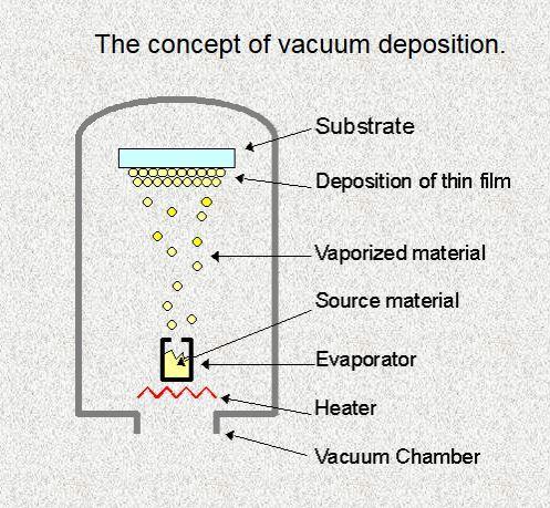
8 Definition of the problem When a polymer is dissolved and then evaporated, the macromolecules break because of their thermal energy. In order to get a thin film of a good quality and with a good adhesion, the polymerization has to happen on the substrate. However, in the vacuum deposition method, this is not happening because the energy of the monomers is low.
9 Information Slide (1) : Ionization-Assisted Method Ionization-Assisted Method is an improvement of the usual evaporation method. An ionizer is added between the evaporator and the substrate in order to ionize a part of the evaporated material. Like a usual evaporation method, it is processed over high vacuum. To get an idea of the importance of the ionization mechanism, one can compare the energies of the particles with or without the ionizer. Without it, a particle gets E=kT/2 from the evaporation. E=0,055eV at 1000 C. With the ionizer polarized with 1V, E=1eV at the same temperature of evaporation which is equivalent to an evaporation at C.
10 Information Slide (2) : The effect of the kinetic energy Like we have seen in the last slide of the presentation, both high kinetic energy and charge of the particle contribute to the higher quality of the polymer layer. The kinetic energy enhances the creation of nucleation site (a), surface migration (b), surface cleaning by sputtering (c) and surface adhesion (d).
11 Information Slide (3) : The effect of the charge The charge acquired by ionization of the particle enhances the nucleation and growth (a), the polymerization (b) and the alignment of the dipoles (c). This last fact can be used to depose effective piezoelectric polymeric layer like with polyurea films.
12 Information Slide (4) : MAPLE MAPLE states for Matrix-Assisted Pulsed Laser Evaporation. The method is base on a consumable frozen target made of the dissolved polymer within a volatile solvent. The target is frozen between -40 and -160 C. A UV light laser pulses on the target which absorbs most of the energy (6,2 ev by pulse at 200nm). This energy is evaporating the target and the rest is then converted to kinetic energy inducing multiple collision within the evaporated particles. This leads to the desorption of the polymer without any damage. The more volatile particle of the solvent are then pumped away while the polymer is deposited directly on the substrate.
13 Information Slide (4) : MAPLE The atmosphere of the chamber must be high vacuum (ultra high vacuum is not needed) or pressurized inert atmosphere with nitrogen for example. Under these conditions, the method is creating really homogeneous films with a thickness from some tens of nanometers according to the number of pulses.
14 References [1] Piqué, A., Auyeung, R., Stepnowski, J., Weir, D., Arnold, C., McGill, R. and Chrisey, D. (2003). Laser processing of polymer thin films for chemical sensor applications. Surface and Coatings Technology, , pp [2] Usui, H. (2000). Polymeric film deposition by ionization-assisted method for optical and optoelectronic applications. Thin Solid Films, 365(1), pp [3] Usui, H. and Tanaka, K. (2016). index. [online] Web.tuat.ac.jp. Available at: [Accessed 19 Feb. 2016].
Pulsed Laser Deposition; laser ablation. Final apresentation for TPPM Diogo Canavarro, MEFT
 Pulsed Laser Deposition; laser ablation Final apresentation for TPPM Diogo Canavarro, 56112 MEFT Summary What is PLD? What is the purpose of PLD? How PLD works? Experimental Setup Processes in PLD The
20.2 Ion Sources. ions electrospray uses evaporation of a charged liquid stream to transfer high molecular mass compounds into the gas phase as MH n
 20.2 Ion Sources electron ionization produces an M + ion and extensive fragmentation chemical ionization produces an M +, MH +, M +, or M - ion with minimal fragmentation MALDI uses laser ablation to transfer
4. How can fragmentation be useful in identifying compounds? Permits identification of branching not observed in soft ionization.
 Homework 9: Chapters 20-21 Assigned 12 April; Due 17 April 2006; Quiz on 19 April 2006 Chap. 20 (Molecular Mass Spectroscopy) Chap. 21 (Surface Analysis) 1. What are the types of ion sources in molecular
Repetition: Practical Aspects
 Repetition: Practical Aspects Reduction of the Cathode Dark Space! E x 0 Geometric limit of the extension of a sputter plant. Lowest distance between target and substrate V Cathode (Target/Source) - +
6.5 Optical-Coating-Deposition Technologies
 92 Chapter 6 6.5 Optical-Coating-Deposition Technologies The coating process takes place in an evaporation chamber with a fully controlled system for the specified requirements. Typical systems are depicted
TMT4320 Nanomaterials November 10 th, Thin films by physical/chemical methods (From chapter 24 and 25)
") 1 TMT4320 Nanomaterials November 10 th, 2015 Thin films by physical/chemical methods (From chapter 24 and 25) 2 Thin films by physical/chemical methods Vapor-phase growth (compared to liquid-phase growth)
1 TMT4320 Nanomaterials November 10 th, 2015 Thin films by physical/chemical methods (From chapter 24 and 25) 2 Thin films by physical/chemical methods Vapor-phase growth (compared to liquid-phase growth)
Fundamentals of Mass Spectrometry. Fundamentals of Mass Spectrometry. Learning Objective. Proteomics
 Mass spectrometry (MS) is the technique for protein identification and analysis by production of charged molecular species in vacuum, and their separation by magnetic and electric fields based on mass
Accelerated Neutral Atom Beam (ANAB)
") Accelerated Neutral Atom Beam (ANAB) Development and Commercialization July 2015 1 Technological Progression Sometimes it is necessary to develop a completely new tool or enabling technology to meet future
Accelerated Neutral Atom Beam (ANAB) Development and Commercialization July 2015 1 Technological Progression Sometimes it is necessary to develop a completely new tool or enabling technology to meet future
Chemistry Instrumental Analysis Lecture 34. Chem 4631
 Chemistry 4631 Instrumental Analysis Lecture 34 From molecular to elemental analysis there are three major techniques used for elemental analysis: Optical spectrometry Mass spectrometry X-ray spectrometry
Lecture 15: Introduction to mass spectrometry-i
 Lecture 15: Introduction to mass spectrometry-i Mass spectrometry (MS) is an analytical technique that measures the mass/charge ratio of charged particles in vacuum. Mass spectrometry can determine masse/charge
Lecture 1: Vapour Growth Techniques
 PH3EC2 Vapour Growth and Epitaxial Growth Lecturer: Dr. Shinoj V K Lecture 1: Vapour Growth Techniques 1.1 Vapour growth The growth of single crystal materials from the vapour phase. Deposition from the
THE PROPERTIES OF THIN FILM DIELECTRIC LAYERS PREPARED BY SPUTTERING
 THE PROPERTIES OF THIN FILM DIELECTRIC LAYERS PREPARED BY SPUTTERING Ivana BESHAJOVÁ PELIKÁNOVÁ a, Libor VALENTA a a KATEDRA ELEKTROTECHNOLOGIE, ČVUT FEL, Technická 2, 166 27 Praha 6, Česká republika,
MICROCHIP MANUFACTURING by S. Wolf
 by S. Wolf Chapter 15 ALUMINUM THIN-FILMS and SPUTTER-DEPOSITION 2004 by LATTICE PRESS CHAPTER 15 - CONTENTS Aluminum Thin-Films Sputter-Deposition Process Steps Physics of Sputter-Deposition Magnetron-Sputtering
Chemical Vapor Deposition *
 OpenStax-CNX module: m25495 1 Chemical Vapor Deposition * Andrew R. Barron This work is produced by OpenStax-CNX and licensed under the Creative Commons Attribution License 3.0 note: This module was developed
Ionization Techniques Part IV
 Ionization Techniques Part IV CU- Boulder CHEM 5181 Mass Spectrometry & Chromatography Presented by Prof. Jose L. Jimenez High Vacuum MS Interpretation Lectures Sample Inlet Ion Source Mass Analyzer Detector
k T m 8 B P m k T M T
 I. INTRODUCTION AND OBJECTIVE OF THE EXPERIENT The techniques for evaporation of chemicals in a vacuum are widely used for thin film deposition on rigid substrates, leading to multiple applications: production
Supplementary Figure 1 Detailed illustration on the fabrication process of templatestripped
 Supplementary Figure 1 Detailed illustration on the fabrication process of templatestripped gold substrate. (a) Spin coating of hydrogen silsesquioxane (HSQ) resist onto the silicon substrate with a thickness
Chapter 4 Scintillation Detectors
 Med Phys 4RA3, 4RB3/6R03 Radioisotopes and Radiation Methodology 4-1 4.1. Basic principle of the scintillator Chapter 4 Scintillation Detectors Scintillator Light sensor Ionizing radiation Light (visible,
Chapter 14. Molar Mass Distribution.
 Chapter 14. Molar Mass Distribution. Difficulty with M n and M w, etc. osome polymers are hard to describe from just M n, M w, etc. o Examples: Bimodal, multimodal, nonuniform, broad, etc. MWDs. oin early
LECTURE 5 SUMMARY OF KEY IDEAS
 LECTURE 5 SUMMARY OF KEY IDEAS Etching is a processing step following lithography: it transfers a circuit image from the photoresist to materials form which devices are made or to hard masking or sacrificial
UNIT 3. By: Ajay Kumar Gautam Asst. Prof. Dev Bhoomi Institute of Technology & Engineering, Dehradun
 UNIT 3 By: Ajay Kumar Gautam Asst. Prof. Dev Bhoomi Institute of Technology & Engineering, Dehradun 1 Syllabus Lithography: photolithography and pattern transfer, Optical and non optical lithography, electron,
Nanostructure. Materials Growth Characterization Fabrication. More see Waser, chapter 2
 Nanostructure Materials Growth Characterization Fabrication More see Waser, chapter 2 Materials growth - deposition deposition gas solid Physical Vapor Deposition Chemical Vapor Deposition Physical Vapor
DEPOSITION OF THIN TiO 2 FILMS BY DC MAGNETRON SPUTTERING METHOD
 Chapter 4 DEPOSITION OF THIN TiO 2 FILMS BY DC MAGNETRON SPUTTERING METHOD 4.1 INTRODUCTION Sputter deposition process is another old technique being used in modern semiconductor industries. Sputtering
Introducing the RoVaCBE Flagship project: Roll-to-roll Vacuum-processed Carbon Based Electronics. Dr Hazel Assender, University of Oxford
 Introducing the RoVaCBE Flagship project: Roll-to-roll Vacuum-processed Carbon Based Electronics Dr Hazel Assender, University of Oxford DALMATIAN TECHNOLOGY 21 st Sept 2010 1 Organic electronics Opportunity
Table of Content. Mechanical Removing Techniques. Ultrasonic Machining (USM) Sputtering and Focused Ion Beam Milling (FIB)
 Sputtering and Focused Ion Beam Milling (FIB)") Table of Content Mechanical Removing Techniques Ultrasonic Machining (USM) Sputtering and Focused Ion Beam Milling (FIB) Ultrasonic Machining In ultrasonic machining (USM), also called ultrasonic grinding,
Table of Content Mechanical Removing Techniques Ultrasonic Machining (USM) Sputtering and Focused Ion Beam Milling (FIB) Ultrasonic Machining In ultrasonic machining (USM), also called ultrasonic grinding,
Chemical Vapor Deposition (CVD)
") Chemical Vapor Deposition (CVD) source chemical reaction film substrate More conformal deposition vs. PVD t Shown here is 100% conformal deposition ( higher temp has higher surface diffusion) t step 1
Chemical Vapor Deposition (CVD) source chemical reaction film substrate More conformal deposition vs. PVD t Shown here is 100% conformal deposition ( higher temp has higher surface diffusion) t step 1
Tailored surface modification of substrates by atmospheric plasma for improved compatibility with specific adhesive Nicolas Vandencasteele
 1 oating Plasma Innovation Tailored surface modification of substrates by atmospheric plasma for improved compatibility with specific adhesive Nicolas Vandencasteele 2 Plasma Applications Adhesion improvement
Chapter 9 Generation of (Nano)Particles by Growth
Particles by Growth") Chapter 9 Generation of (Nano)Particles by Growth 9.1 Nucleation (1) Supersaturation Thermodynamics assumes a phase change takes place when there reaches Saturation of vapor in a gas, Saturation of solute
Chapter 9 Generation of (Nano)Particles by Growth 9.1 Nucleation (1) Supersaturation Thermodynamics assumes a phase change takes place when there reaches Saturation of vapor in a gas, Saturation of solute
Nova 600 NanoLab Dual beam Focused Ion Beam IITKanpur
 Nova 600 NanoLab Dual beam Focused Ion Beam system @ IITKanpur Dual Beam Nova 600 Nano Lab From FEI company (Dual Beam = SEM + FIB) SEM: The Electron Beam for SEM Field Emission Electron Gun Energy : 500
Mat. Res. Soc. Symp. Proc. Vol Materials Research Society. Novel Growth of Biodegradable Thin Films via Matrix Assisted Laser Processing
 Mat. Res. Soc. Symp. Proc. Vol. 780 2003 Materials Research Society Y4.4.1 Novel Growth of Biodegradable Thin Films via Matrix Assisted Laser Processing A.L. Mercado 1, J.M. Fitz-Gerald 1, R. Johnson 2,
Chemistry 311: Topic 3 - Mass Spectrometry
 Mass Spectroscopy: A technique used to measure the mass-to-charge ratio of molecules and atoms. Often characteristic ions produced by an induced unimolecular dissociation of a molecule are measured. These
Other Methods for Generating Ions 1. MALDI matrix assisted laser desorption ionization MS 2. Spray ionization techniques 3. Fast atom bombardment 4.
 Other Methods for Generating Ions 1. MALDI matrix assisted laser desorption ionization MS 2. Spray ionization techniques 3. Fast atom bombardment 4. Field Desorption 5. MS MS techniques Matrix assisted
Surface Engineering of Nanomaterials Dr. Kaushik Pal Department of Mechanical and Industrial Engineering Indian Institute of Technology, Roorkee
 Surface Engineering of Nanomaterials Dr. Kaushik Pal Department of Mechanical and Industrial Engineering Indian Institute of Technology, Roorkee Lecture 11 Deposition and Surface Modification Methods So,
Introduction to Thin Film Processing
 Introduction to Thin Film Processing Deposition Methods Many diverse techniques available Typically based on three different methods for providing a flux of atomic or molecular material Evaporation Sputtering
Repetition: Physical Deposition Processes
 Repetition: Physical Deposition Processes PVD (Physical Vapour Deposition) Evaporation Sputtering Diode-system Triode-system Magnetron-system ("balanced/unbalanced") Ion beam-system Ionplating DC-glow-discharge
Electrical Discharges Characterization of Planar Sputtering System
 International Journal of Recent Research and Review, Vol. V, March 213 ISSN 2277 8322 Electrical Discharges Characterization of Planar Sputtering System Bahaa T. Chaid 1, Nathera Abass Ali Al-Tememee 2,
CHAPTER 7 SUMMARY OF THE PRESENT WORK AND SUGGESTIONS FOR FUTURE WORK
 161 CHAPTER 7 SUMMARY OF THE PRESENT WORK AND SUGGESTIONS FOR FUTURE WORK 7.1 SUMMARY OF THE PRESENT WORK Nonlinear optical materials are required in a wide range of important applications, such as optical
Tutorial on Plasma Polymerization Deposition of Functionalized Films
 Tutorial on Plasma Polymerization Deposition of Functionalized Films A. Michelmore, D.A. Steele, J.D. Whittle, J.W. Bradley, R.D. Short University of South Australia Based upon review article RSC Advances,
Molecular dynamics simulation study of the ejection and transport of polymer molecules in matrix-assisted pulsed laser evaporation
 JOURNAL OF APPLIED PHYSICS 102, 074914 2007 Molecular dynamics simulation study of the ejection and transport of polymer molecules in matrix-assisted pulsed laser evaporation Elodie Leveugle and Leonid
Application of the GD-Profiler 2 to the PV domain
 Application of the GD-Profiler 2 to the PV domain GD Profiler 2 RF GDOES permits to follow the distribution of the elements as function of depth. This is an ultra fast characterisation technique capable
Techniken der Oberflächenphysik (Techniques of Surface Physics)
") Techniken der Oberflächenphysik (Techniques of Surface Physics) Prof. Yong Lei & Dr. Yang Xu (& Liying Liang) Fachgebiet 3D-Nanostrukturierung, Institut für Physik Contact: yong.lei@tu-ilmenau.de; yang.xu@tu-ilmenau.de;
Techniken der Oberflächenphysik (Techniques of Surface Physics) Prof. Yong Lei & Dr. Yang Xu (& Liying Liang) Fachgebiet 3D-Nanostrukturierung, Institut für Physik Contact: yong.lei@tu-ilmenau.de; yang.xu@tu-ilmenau.de;
Metallurgical and Materials Engineering Department MME 2509 Materials Processing Laboratory SOL-GEL DIP COATING
 Metallurgical and Materials Engineering Department MME 2509 Materials Processing Laboratory SOL-GEL DIP COATING Assist. Prof. Dr. Tolga TAVŞANOĞLU 1. Sol-gel Process Sol-gel process is used for production
White Paper Adhesives Sealants Tapes
 Fundamental principles of UV reactive manufacturing processes Introduction While the UV systems technology and the appropriate chemistry have been developing continuously, the principle of irradiation
Abstract. Introduction
 Organic Materials in Optoelectronic Applications: Physical Processes and Active Devices Jonnalagadda Padmarani Department of Physics (Opto Electronics), Osmania University, TS, India Abstract The present
Chapter 10. Nanometrology. Oxford University Press All rights reserved.
 Chapter 10 Nanometrology Oxford University Press 2013. All rights reserved. 1 Introduction Nanometrology is the science of measurement at the nanoscale level. Figure illustrates where nanoscale stands
Introduction to Photolithography
 http://www.ichaus.de/news/72 Introduction to Photolithography Photolithography The following slides present an outline of the process by which integrated circuits are made, of which photolithography is
Analysis of Poly(dimethylsiloxane) on Solid Surfaces Using Silver Deposition/TOF-SIMS
 on Solid Surfaces Using Silver Deposition/TOF-SIMS") Special Issue Surface and Micro-Analysis of Organic Materials 21 Research Report Analysis of Poly(dimethylsiloxane) on Solid Surfaces Using Silver Deposition/TOF-SIMS Masae Inoue, Atsushi Murase Abstract
Special Issue Surface and Micro-Analysis of Organic Materials 21 Research Report Analysis of Poly(dimethylsiloxane) on Solid Surfaces Using Silver Deposition/TOF-SIMS Masae Inoue, Atsushi Murase Abstract
Film Deposition Part 1
 1 Film Deposition Part 1 Chapter 11 : Semiconductor Manufacturing Technology by M. Quirk & J. Serda Spring Semester 2013 Saroj Kumar Patra Semidonductor Manufacturing Technology, Norwegian University of
Introduction. Photoresist : Type: Structure:
 Photoresist SEM images of the morphologies of meso structures and nanopatterns on (a) a positively nanopatterned silicon mold, and (b) a negatively nanopatterned silicon mold. Introduction Photoresist
Section 5: Thin Film Deposition part 1 : sputtering and evaporation. Jaeger Chapter 6. EE143 Ali Javey
 Section 5: Thin Film Deposition part 1 : sputtering and evaporation Jaeger Chapter 6 Vacuum Basics 1. Units 1 atmosphere = 760 torr = 1.013x10 5 Pa 1 bar = 10 5 Pa = 750 torr 1 torr = 1 mm Hg 1 mtorr =
Modern Methods in Heterogeneous Catalysis Research: Preparation of Model Systems by Physical Methods
 Modern Methods in Heterogeneous Catalysis Research: Preparation of Model Systems by Physical Methods Methods for catalyst preparation Methods discussed in this lecture Physical vapour deposition - PLD
Lecture 8: Mass Spectrometry
 intensity Lecture 8: Mass Spectrometry Relative abundance m/z 1 Ethylbenzene experiment CH 2 CH 3 + m/z = 106 CH 2 + m/z = 91 C 8 H 10 MW = 106 CH + m/z = 77 + 2 2 What information can we get from MS spectrum?
Update in Material and Process Technologies for 2.5/3D IC Dr. Rainer Knippelmeyer CTO and VP R&D, SÜSS MicroTec AG
 Update in Material and Process Technologies for 2.5/3D IC Dr. Rainer Knippelmeyer CTO and VP R&D, SÜSS MicroTec AG TEMPORARY BONDING / DEBONDING AS THIN WAFER HANDLING SOLUTION FOR 3DIC & INTERPOSERS Device
Lecture 8: Mass Spectrometry
 intensity Lecture 8: Mass Spectrometry Relative abundance m/z 1 Ethylbenzene CH 2 CH 3 + m/z = 106 CH 2 + m/z = 91 C 8 H 10 MW = 106 CH + m/z = 77 + 2 2 What information can be obtained from a MS spectrum?
M. Audronis 1 and F. Zimone 2 1. Nova Fabrica Ltd. 1. Angstrom Sciences Inc.
 M. Audronis 1 and F. Zimone 2 1 Nova Fabrica Ltd. 1 Angstrom Sciences Inc. Email: info@novafabrica.biz 1 Founded in 2013 the company is based in Lithuania (northern EU). NF are involved in two business
Repetition: Ion Plating
 Repetition: Ion Plating Substrate HV (bis ca. 1kV) Optional ionization system Source Ionized filling gas Source material, ionized or neutral Repetition: Ion Plating Ion Species Separated ion source Ions
International Journal of Science, Environment and Technology, Vol. 6, No 2, 2017,
 International Journal of Science, Environment and Technology, Vol. 6, No 2, 2017, 1476 1480 ISSN 2278-3687 (O) 2277-663X (P) MORPHOLOGICAL STUDY OF CDSE QUANTUM DOTS IN POLY (3-HEXYLTHIOPHENE)(P3HT) PREPARED
FRAUNHOFER INSTITUTE FOR SURFACE ENGINEERING AND THIN FILMS IST ATMOSPHERIC PRESSURE PLASMA PROCESSES
 FRAUNHOFER INSTITUTE FOR SURFACE ENGINEERING AND THIN FILMS IST ATMOSPHERIC PRESSURE PLASMA PROCESSES 1 2 ATMOSPHERIC PRESSURE PLASMA PROCESSES AT THE FRAUNHOFER IST Today, atmospheric pressure plasma
PHYSICAL VAPOR DEPOSITION OF THIN FILMS
 PHYSICAL VAPOR DEPOSITION OF THIN FILMS JOHN E. MAHAN Colorado State University A Wiley-Interscience Publication JOHN WILEY & SONS, INC. New York Chichester Weinheim Brisbane Singapore Toronto CONTENTS
Harmonic Generation for Photoionization Experiments Christian J. Kornelis Physics REU Kansas State University
 Harmonic Generation for Photoionization Experiments Christian J. Kornelis Physics REU Kansas State University The Basic Setup for the KLS Photoionization Experiment V. Kumarappan Femtosecond Pump-Probe
Behavior of Three Types of Plasma Sources for Optical Coating
 Behavior of Three Types of Plasma Sources for Optical Coating Ronald R. Willey Willey Optical, Consultants, 13039 Cedar Street, Charlevoix, MI 49720, USA Ph 231-237-9392, ron@willeyoptical.com ABSTRACT
Laser Deposition of Tetrasulfonated Phthalocyanine Layers for Gas Sensors
 Advances in Materials Physics and Chemistry, 2012, 2, 84-88 doi:10.4236/ampc.2012.24b023 Published Online December 2012 (http://www.scirp.org/journal/ampc) Laser Deposition of Tetrasulfonated Phthalocyanine
Introduction to Plasma
 What is a plasma? The fourth state of matter A partially ionized gas How is a plasma created? Energy must be added to a gas in the form of: Heat: Temperatures must be in excess of 4000 O C Radiation Electric
Wet and Dry Etching. Theory
 Wet and Dry Etching Theory 1. Introduction Etching techniques are commonly used in the fabrication processes of semiconductor devices to remove selected layers for the purposes of pattern transfer, wafer
Garden City High School Science Department Honors Living Environment Summer Assignment
 Garden City High School Science Department Honors Living Environment Summer Assignment Each student anticipating enrollment in the Honors Living Environment course will be required to complete a summer
Laser processing of polymer nanocomposite thin films
 Laser processing of polymer nanocomposite thin films A. T. Sellinger, E. M. Leveugle, K. Gogick, L. V. Zhigilei, and J. M. Fitz-Gerald a Department of Materials Science and Engineering, University of Virginia,
Supplementary Information Our InGaN/GaN multiple quantum wells (MQWs) based one-dimensional (1D) grating structures
 based one-dimensional (1D) grating structures") Polarized white light from hybrid organic/iii-nitrides grating structures M. Athanasiou, R. M. Smith, S. Ghataora and T. Wang* Department of Electronic and Electrical Engineering, University of Sheffield,
Polarized white light from hybrid organic/iii-nitrides grating structures M. Athanasiou, R. M. Smith, S. Ghataora and T. Wang* Department of Electronic and Electrical Engineering, University of Sheffield,
Secondary ion mass spectrometry (SIMS)
") Secondary ion mass spectrometry (SIMS) ELEC-L3211 Postgraduate Course in Micro and Nanosciences Department of Micro and Nanosciences Personal motivation and experience on SIMS Offers the possibility to
Secondary ion mass spectrometry (SIMS) ELEC-L3211 Postgraduate Course in Micro and Nanosciences Department of Micro and Nanosciences Personal motivation and experience on SIMS Offers the possibility to
Energy fluxes in plasmas for fabrication of nanostructured materials
 Energy fluxes in plasmas for fabrication of nanostructured materials IEAP, Universität Kiel 2nd Graduate Summer Institute "Complex Plasmas" August 5-13, 2010 in Greifswald (Germany) AG 1 Outline Motivation
Atmospheric Plasma treatment, effect on the plasma chemistry on adhesion Nicolas Vandencasteele
 1 oating Plasma Innovation Atmospheric Plasma treatment, effect on the plasma chemistry on adhesion Nicolas Vandencasteele 2 Plasma Applications Adhesion improvement onclusion 3 Plasma 4 th state of matter:
Déposition séléctive le rêve reviens
 Willkommen Welcome Bienvenue Déposition séléctive le rêve reviens Patrik Hoffmann Michael Reinke, Yury Kuzminykh Ivo Utke, Carlos Guerra-Nunez, Ali Dabirian, Xavier Multone, Tristan Bret, Estelle Halary-Wagner,
Ever come to work. And get the feeling it s not going to be such a good day?
 Ever come to work And get the feeling it s not going to be such a good day? Water The Key To Life On Earth (or one of them, anyway) Why Water Is Your Friend Water has several properties which make life
Top down and bottom up fabrication
 Lecture 24 Top down and bottom up fabrication Lithography ( lithos stone / graphein to write) City of words lithograph h (Vito Acconci, 1999) 1930 s lithography press Photolithography d 2( NA) NA=numerical
Effect of Spiral Microwave Antenna Configuration on the Production of Nano-crystalline Film by Chemical Sputtering in ECR Plasma
 THE HARRIS SCIENCE REVIEW OF DOSHISHA UNIVERSITY, VOL. 56, No. 1 April 2015 Effect of Spiral Microwave Antenna Configuration on the Production of Nano-crystalline Film by Chemical Sputtering in ECR Plasma
Chemistry Instrumental Analysis Lecture 17. Chem 4631
 Chemistry 4631 Instrumental Analysis Lecture 17 Introduction to Optical Atomic Spectrometry From molecular to elemental analysis there are three major techniques used for elemental analysis: Optical spectrometry
EE143 Fall 2016 Microfabrication Technologies. Lecture 6: Thin Film Deposition Reading: Jaeger Chapter 6
 EE143 Fall 2016 Microfabrication Technologies Lecture 6: Thin Film Deposition Reading: Jaeger Chapter 6 Prof. Ming C. Wu wu@eecs.berkeley.edu 511 Sutardja Dai Hall (SDH) 1 Vacuum Basics Units 1 atmosphere
Molecular weight of polymers. Molecular weight of polymers. Molecular weight of polymers. Molecular weight of polymers. H i
 Gel Permeation Chromatography (GPC) : Size Exclusion Chromatography GPC : 1. Chromatogram (V R vs H) H i Detector response Baseline N i M i 130 135 140 145 150 155 160 165 Elution volume (V R ) (counts)
Plasma Deposition (Overview) Lecture 1
 Lecture 1") Plasma Deposition (Overview) Lecture 1 Material Processes Plasma Processing Plasma-assisted Deposition Implantation Surface Modification Development of Plasma-based processing Microelectronics needs (fabrication
Plasma Deposition (Overview) Lecture 1 Material Processes Plasma Processing Plasma-assisted Deposition Implantation Surface Modification Development of Plasma-based processing Microelectronics needs (fabrication
OPTIMIZATION OF DIELECTRICS SURFACE PREPARATION FOR VACUUM COATING
 OPTIMIZATION OF DIELECTRICS SURFACE PREPARATION FOR VACUUM COATING Dr. Boris Statnikov Introduction Modern MICRO and NANO technologies in ultra- and high-frequency electronics are widely focused on application
Supporting information. and/or J -aggregation. Sergey V. Dayneko, Abby-Jo Payne and Gregory C. Welch*
 Supporting information Inverted P3HT:PC61BM organic solar cells incorporating a -extended squaraine dye with H- and/or J -aggregation. Sergey V. Dayneko, Abby-Jo Payne and Gregory C. Welch* Department
Proportional Counters
 Proportional Counters 3 1 Introduction 3 2 Before we can look at individual radiation processes, we need to understand how the radiation is detected: Non-imaging detectors Detectors capable of detecting
Dielectric constant measurement of P3HT, polystyrene, and polyethylene
 Dielectric constant measurement of P3HT, polystyrene, and polyethylene Supervisor: prof. dr. J.C. Hummelen Daily supervisor: Jenny Douvogianni Name: Si Chen (s2660482) 1. Introduction Dielectric constant
Preparation of Nanostructures(Příprava Nanostruktur)
") Preparation of Nanostructures (Příprava Nanostruktur) jaroslav.hamrle@vsb.cz September 23, 2013 Outline 1 Introduction 2 Bulk crystal growth 3 Thin film preparation 4 Lateral structures 5 Surface plasma
Preparation of Nanostructures (Příprava Nanostruktur) jaroslav.hamrle@vsb.cz September 23, 2013 Outline 1 Introduction 2 Bulk crystal growth 3 Thin film preparation 4 Lateral structures 5 Surface plasma
SUPPLEMENTARY INFORMATION
 doi:10.1038/nature11231 Materials and Methods: Sample fabrication: Highly oriented VO 2 thin films on Al 2 O 3 (0001) substrates were deposited by reactive sputtering from a vanadium target through reactive
Sciences and Analyses of Materials Department Surface Treatment Unit Centre de Recherche Public Gabriel Lippmann Belvaux - Luxembourg
 Sciences and Analyses of Materials Department Surface Treatment Unit Centre de Recherche Public Gabriel Lippmann Belvaux - Luxembourg Surface Treatment Unit, UTS BRIEF history : 2006 2009 : launched of
Thin and Ultrathin Plasma Polymer Films and Their Characterization
 WDS'13 Proceedings of Contributed Papers, Part III, 134 138, 2013. ISBN 978-80-7378-252-8 MATFYZPRESS Thin and Ultrathin Plasma Polymer Films and Their Characterization M. Petr, O. Kylián, J. Hanuš, A.
Deposition of thin films
 16 th March 2011 The act of applying a thin film to a surface is thin-film deposition - any technique for depositing a thin film of material onto a substrate or onto previously deposited layers. Thin is
Lecture 22 Ion Beam Techniques
 Lecture 22 Ion Beam Techniques Schroder: Chapter 11.3 1/44 Announcements Homework 6/6: Will be online on later today. Due Wednesday June 6th at 10:00am. I will return it at the final exam (14 th June).
CHAPTER 6: Etching. Chapter 6 1
 Chapter 6 1 CHAPTER 6: Etching Different etching processes are selected depending upon the particular material to be removed. As shown in Figure 6.1, wet chemical processes result in isotropic etching
Supporting Information
 Supporting Information Irreversible Visual Sensing of Humidity Using a Cholesteric Liquid Crystal Abhijit Saha, a Yoko Tanaka, a Yang Han, a Cees M. W. Bastiaansen, b Dirk J. Broer b and Rint P. Sijbesma*
Understanding electron energy loss mechanisms in EUV resists using EELS and first-principles calculations
 Understanding electron energy loss mechanisms in EUV resists using EELS and first-principles calculations Robert Bartynski Sylvie Rangan Department of Physics & Astronomy and Laboratory for Surface Modification
Proudly serving laboratories worldwide since 1979 CALL for Refurbished & Certified Lab Equipment
 www.ietltd.com Proudly serving laboratories worldwide since 1979 CALL +1.847.913.0777 for Refurbished & Certified Lab Equipment Applied Biosystems QStar Pulsar i Features of the API QSTAR Pulsar i The
High Performance, Low Operating Voltage n-type Organic Field Effect Transistor Based on Inorganic-Organic Bilayer Dielectric System
 Journal of Physics: Conference Series PAPER OPEN ACCESS High Performance, Low Operating Voltage n-type Organic Field Effect Transistor Based on Inorganic-Organic Bilayer Dielectric System To cite this
THE VACUUM DEPOSITION OF POLYIMIDE LAYERS IN THE PRESENCE
 THE VACUUM DEPOSITION OF POLYIMIDE LAYERS IN THE PRESENCE OF AN INERT GAS ANOTHER TECHNOLOGICAL SOLUTION FOR PRODUCING LOW DIELECTRIC CONSTANT MATERIALS Velichka Jordanova Strijkova 1, Ivaylo Tzankov Zhivkov,
Water and Aqueous Systems
 Water and Aqueous Systems Chemistry CP http://www.sumanasinc.com/webcontent/animations/content/ propertiesofwater/water.html The Water Molecule Bent Two lone electron pairs Polar molecule Considered to
Structuring and bonding of glass-wafers. Dr. Anke Sanz-Velasco
 Structuring and bonding of glass-wafers Dr. Anke Sanz-Velasco Outline IMT Why glass? Components for life science Good bond requirements and evaluation Wafer bonding 1. Fusion bonding 2. UV-adhesive bonding
Vacuum Pumps. Two general classes exist: Gas transfer physical removal of matter. Mechanical, diffusion, turbomolecular
 Vacuum Technology Vacuum Pumps Two general classes exist: Gas transfer physical removal of matter Mechanical, diffusion, turbomolecular Adsorption entrapment of matter Cryo, sublimation, ion Mechanical
This activity has been used in an introductory chemistry course (prep chemistry or GOB course) Learning Goals: Prerequisite knowledge
 Learning Goals: Prerequisite knowledge") This activity has been used in an introductory chemistry course (prep chemistry or GOB course) Learning Goals: Name phase changes Identify phase changes at molecular (particulate) level Name intermolecular
This activity has been used in an introductory chemistry course (prep chemistry or GOB course) Learning Goals: Name phase changes Identify phase changes at molecular (particulate) level Name intermolecular
The design of an integrated XPS/Raman spectroscopy instrument for co-incident analysis
 The design of an integrated XPS/Raman spectroscopy instrument for co-incident analysis Tim Nunney The world leader in serving science 2 XPS Surface Analysis XPS +... UV Photoelectron Spectroscopy UPS He(I)
General Chem Solution.notebook. Solutions. Mar 12 8:19 AM
 General Chem Solution.notebook Solutions Mar 12 8:19 AM 1 Solutions 2015 OBJECTIVES: 1. I can distinguish between a heterogeneous and a homogeneous solution. 2. I can list different solute solvent combinations.