Energy Bands in Solids. Prof.P. Ravindran, Department of Physics, Central University of Tamil Nadu, India
|
|
|
- Ashlie Hudson
- 5 years ago
- Views:
Transcription
1 Energy Bands in Solids 1 Prof.P. Ravindran, Department of Physics, Central University of Tamil Nadu, India
2 Electrons in Solids Considering electrons in metals as free particles, electron gas in a box explains many experimental results which? Still, why are some solids metals and others insulators? For metals we assumed that electrons are free We know, however, that there are no free electrons in insulators QM give us the answer! Need a more realistic potential for electrons reflecting periodic ionic structure of solids

3 Splitting of Energy levels If the atoms are far apart- atoms can be considered as isolated Under the influence of neighbouring atoms- splitting of energy levels occurs The width of K-shell is less as compared to L-shell and so on Effect of distance on splitting of energy levels
4 Energy E3 (M shell) E2 (L shell) E1 (K shell)
5 Band Energy Energy Band Forbidden Energy Gap Energy Band
6 ENERGY BANDS IN SOLIDS Explains and distinguish between conductors, insulators and semi conductors Conduction Band small energy can remove an electron from an atom Valence Band Below the conduction band Filled Band- Near the nucleus Insulators- Conduction band is empty but valence is almost completely filled+ wide energy gap between the two bands (Poor conductivity) Conductors- Overlapping of both conduction and valence bands Conduction es move almost twice as fast as holes
7 Realistic Potential in Solids n i are integers Example: 2D Lattice c n b n a n T T U r U r ) ( ) ( 3 ; n n b n n a T
8 Realistic Potential in Solids For one dimensional case where atoms (ions) are separated by distance d, we can write condition of periodicity as U( x) U( x dn)
9 Realistic Potential in Solids Multi-electron atomic potentials are complex Even for hydrogen atom with a simple Coulomb potential solutions are quite complex So we use a model one-dimensional periodic potential to get insight into the problem
10
 uk(r) i(kr) where u has the period of the lattice, that is u r) u k ( k (r")
11 Bloch Functions Felix Bloch showed that the actual solutions to the Schrödinger equation for electrons in a periodic potential must have the special form: k (r) uk(r) i(kr) where u has the period of the lattice, that is u r) u k ( k (r e T)
12 Bloch s Theorem Bloch s Theorem states that for a particle moving in the periodic potential, the wavefunctions ψ(x) are of the form ( x) u k ( x) e ikx, whereu u k k ( x) u ( x) is a pe riodicfunction k ( x d) u k (x) is a periodic function with the periodicity of the potential The exact form depends on the potential associated with atoms (ions) that form the solid
13 Bloch s Theorem Bloch s Theorem imposes very special conditions on any solution of the Schrödinger equation, independent of the form of the periodic potential The wave vector k has a two-fold role: 1. It is still a wave vector in the plane wave part of the solution 2. It is also an index to u k (x) because it contains all the quantum numbers, which enumerate the wavefunction
14 Bloch s Theorem What is probability density of finding particle at coordinate x? 2 * * * * 2 ) ( ) ( ) ( ) ( ) ( ) ( ) ( ] ) ( [ ] ) ( [ ) ( ) ( ) ( ) ( ) ( x u x P x u x u e e x u x u x P e x u e x u x P x x x x P k k k ikx ikx k k ikx k ikx k But uk(x) 2 is periodic, so P(x) is as well 2 (x) u k
15 Bloch s Theorem P( x) P( x d) The probability of finding an electron at any atom in the solid is the same!!! Each electron in a crystalline solid belongs to each and every atom forming the solid
16 Kronig-Penney Model U(x) U0 (a+b) b 0 a a+b x The wave equation can be solved when the potential is simple... such as a periodic square well.
17 Kronig-Penney Model 2 2 d U( x) 2m 2 dx Region I - where 0 < x < a and U = 0 The eigenfunction is a linear combination of plane waves traveling both left and right: Ae ikx Be ikx The energy eignevalue is: 2 K 2m 2


18 Kronig-Penney Model 2 2 d U( x) 2m 2 dx Region II - where b < x < 0 and U = U0 Within the barrier, the eigenfunction looks like this Ce Qx De Qx and U 0 2 Q 2m 2
19 Kronig-Penney Model U(x) U0 II I III (a+b) b 0 a a+b x To satisfy Mr. Bloch, the solution in region III must also be related to the solution in region II. III II e ik ( ab)
20 Kronig-Penney Model A,B,C, and D are chosen so that both the wavefunction and its derivative with respect to x are continuous at the x = 0 and a. At x = 0... A B C D ik( A B) Q( C D) At x = a... III II e ik ( ab) Ae ika Be ika ( Ce Qb De Qb ) e ik( ab) ika ika Qb Qb ik( a b) Be Q Ce De e ik Ae
21 Result for E < U 0 : Kronig-Penney Model 2 Q K 2QK 2 sinhqb sin Ka coshqb cos Ka cos k( a b) To obtain a more convenient form Kronig and Penney considered the case where the potential barrier becomes a delta function, that is, the case where U 0 is infinitely large, over an infinitesimal distance b, but the product U0b remains finite and constant. 2 Q U and also goes to infinity as U 0. Therefore: 0 Lim U0 ( Q 2 K 2 ) Q 2
22 Kronig-Penney Model What happens to the product Qb as U0 goes to infinity? b becomes infinitesimal as U 0 becomes infinite. However, since Q is only proportional to the square root of U 0, it does not go to infinity as fast as b goes to zero. So, the product Qb goes to zero as U 0 becomes infinite. As a results of all of this... sinqb Qb cos Qb 1 Q K 1
23 Kronig-Penney Model P Q 2 ba 2 P Ka sin Ka cos Ka cos ka


24 Kronig-Penney Model Plot of energy versus wavenumber for the Kronig-Penney Potential, with P = 3/ ka 0 ka
25 Covalent Bonding Revisited When atoms are covalently bonded electrons supplied by atoms are shared by these atoms since pull of each atom is the same or nearly so H 2, F 2, CO, Example: the ground state of the hydrogen atoms forming a molecule If the atoms are far apart there is very little overlap between their wavefunctions If atoms are brought together the wavefunctions overlap and form the compound wavefunction, ψ 1 (r)+ψ 2 (r), increasing the probability for electrons to exist between the atoms 1s 1 r / a a 3 0 e 0
26 Schrödinger Equation Revisited If a wavefunctions ψ 1 (x) and ψ 2 (x) are solutions for the Schrödinger equation for energy E, then functions -ψ 1 (x), -ψ 2 (x), and ψ 1 (x)±ψ 2 (x) are also solutions of this equations the probability density of -ψ 1 (x) is the same as for ψ 1 (x) 2 2m d d 2m dx 1,2 2 ( x) U( x)[ 1,2 ( x)] E [ 1( x) 2( x)] U( x)[ 1( x) 2( x)] 2 dx 1,2 ( x) E[ ( x) ( x)] 1 2
27 Band Theory of Solids Consider an atom with only one electron in s-state outside of a closed shell Both of the wavefunctions below are valid and the choice of each is equivalent s s ( r) ( r) Af Af ( r) e ( r) e Zr/ na Zr/ na 0 0 If the atoms are far apart, as before, the wavefunctions are the same as for the isolated atoms
28 Band Theory of Solids Once the atoms are brought together the wavefunctions begin to overlap There are two possibilities 1. Overlapping wavefunctions are the same (e.g., ψ s+ (r)) 2. Overlapping wavefunctions are different The sum of them is shown in the figure These two possible combinations represent two possible states of two atoms system with different energies

29 Symmetric and Anti-symmetric Combinations of Ground State Eigenfunctions
30 Six States for Six Atom Solid
31 Splitting of 1s State of Six Atoms
 are closer to each other than the inner electrons Thus, the overlap of the wavefunctions of the outer electrons is stronger than overlap of those of inner")
32 Atoms and Band Structure Consider multi-electron atoms: 1. The outer electrons (large n and l) are closer to each other than the inner electrons Thus, the overlap of the wavefunctions of the outer electrons is stronger than overlap of those of inner electrons Therefore, the bands formed from outer electrons are wider than the bands formed from inner electrons Bands with higher energies are therefore wider!
33 Splitting of Atomic Levels in Sodium

34 Occupation of Bands Sodium
35 Splitting of Atomic Levels in Carbon


36 Occupation in Carbon at Large Atomic Separation

37 Actual Occupation of Energy bands in Diamond


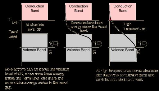
38 Insulators, Semiconductors, Metals The last completely filled (at least at T = 0 K) band is called the Valence Band The next band with higher energy is the Conduction Band The Conduction Band can be empty or partially filed The energy difference between the bottom of the CB and the top of the VB is called the Band Gap (or Forbidden Gap)
39 Insulators, Semiconductors, Metals Consider a solid with the empty Conduction Band If apply electric field to this solid, the electrons in the valence band (VB) cannot participate in transport (no current)
![Insulators, Semiconductors, Metals The electrons in the VB do not participate in the current, since Classically, electrons in the electric field accelerate, so they acquire [kinetic] energy In QM](/docs-images/89/98812942/images/40-6.jpg "this means they must acquire slightly higher energy and jump to another quantum state Such states must be available, i.e. empty allowed states But no such state are available in the VB!")
40 Insulators, Semiconductors, Metals The electrons in the VB do not participate in the current, since Classically, electrons in the electric field accelerate, so they acquire [kinetic] energy In QM this means they must acquire slightly higher energy and jump to another quantum state Such states must be available, i.e. empty allowed states But no such state are available in the VB! This solid would behave as an insulator
 If an")


41 Insulators, Semiconductors, Metals Consider a solid with the half filled Conduction Band (T = 0K) If an electric field is applied to this solid, electrons in the CB do participate in transport, since there are plenty of empty allowed states with energies just above the Fermi energy This solid would behave as a conductor (metal)
42 Band Overlap Many materials are conductors (metals) due to the band overlap phenomenon Often the higher energy bands become so wide that they overlap with the lower bands additional electron energy levels are then available
43 Band Overlap Example: Magnesium (Mg; Z =12): 1s 2 2s 2 2p 6 3s 2 Might expect to be insulator; however, it is a metal 3s-band overlaps the 3p-band, so now the conduction band contains 8N energy levels, while only have 2N electrons Other examples: Zn, Be, Ca, Bi
44 Band Hybridization In some cases the opposite occurs Due to the overlap, electrons from different shells form hybrid bands, which can be separated in energy Depending on the magnitude of the gap, solids can be insulators (Diamond); semiconductors (Si, Ge, Sn; metals (Pb)
45 Insulators, Semiconductors, Metals There is a qualitative difference between metals and insulators (semiconductors) the highest energy band containing electrons is only partially filled for Metals (sometimes due to the overlap) Thus they are good conductors even at very low temperatures The resistivity arises from the electron scattering from lattice vibrations and lattice defects Vibrations increases with temperature higher resistivity The concentration of carriers does not change appreciably with temperature

46 Insulators, Semiconductors, Metals The difference between Insulators and Semiconductors is quantitative The difference in the magnitude of the band gap Semiconductors are Insulators with a relatively small band gap At high enough temperatures a fraction of electrons can be found in the conduction band and therefore participate in transport. Hence resistivity decrease with increase of temperature in semiconductor.
47 Insulators vs Semiconductors There is no difference between Insulators and Semiconductors at very low temperatures In neither material are there any electrons in the conduction band and so conductivity vanishes in the low temperature limit

48 Insulators vs Semiconductors Differences arises at high temperatures A small fraction of the electrons is thermally excited into the conduction band. These electrons carry current just as in metals The smaller the gap the more electrons in the conduction band at a given temperature Resistivity decreases with temperature due to higher concentration of electrons in the conduction band in semiconductore. 1 q 2 n m *
49 Holes Consider an insulator (or semiconductor) with a few electrons excited from the valence band into the conduction band Apply an electric field Now electrons in the valence band have some energy sates into which they can move The movement is complicated since it involves ~ electrons

50 Concept of Holes Consider a semiconductor with a small number of electrons excited from the valence band into the conduction band If an electric field is applied, the conduction band electrons will participate in the electrical current the valence band electrons can move into the empty states, and thus can also contribute to the current
 than electrons since they represent collective behavior of many electrons in the VB (i.e. low lying energy band)")
51 Holes from the Band Structure Point of View If we describe such changes via movement of the empty states the picture can be significantly simplified This empty space is a Hole Deficiency of negative charge holes are positively charged Holes often have a larger effective mass (heavier) than electrons since they represent collective behavior of many electrons in the VB (i.e. low lying energy band)

52 Holes We can replace electrons at the top of e th band which have negative mass (and travel in opposite to the normal direction) by positively charged particles with a positive mass, and consider all phenomena using such particles Such particles are called Holes Holes are positively charged and move in the opposite direction as electrons they replace
53 Hole Conduction To understand hole motion, one requires another view of the holes, which represent them as electrons with negative effective mass To imagine the movement of the hole think of a row of chairs occupied by people with one chair empty To move all people rise all together and move in one direction, so the empty spot moves in the opposite direction
54 Concept of Holes If we describe such changes via movement of the empty states the picture will be significantly simplified This empty space is called a Hole Deficiency of negative charge can be treated as a positive charge Holes act as charge carriers in the sense that electrons from nearby sites can move into the hole Holes are usually heavier than electrons since they depict collective behavior of many electrons

55 Conduction Electrical current for holes and electrons in the opposite direction
56 What are quantum numbers? Quantum numbers label eigenenergies and eigenfunctions of a Hamiltonian Sommerfeld: k-vector ( k is momentum) Bloch: -vector ( is the crystal momentum) and n k k (the band index). The Crystal Momentum is not the Momentum of a Bloch electron: the rate of change of an electron momentum is given by the total forces on the electron, but the rate of change of electronic crystal momentum is: dr dt 1 n( k) d k v ( ) ˆ n k n k v n k ; ee( r, t) vn( k) B( r, t) k dt where forces are exerted only by the external fields, and not by the periodic field of the lattice.
57 Semiclassical dynamics of Bloch electrons Bloch states have the property that their expectation values of and, follow classical dynamics. The only change is that now ( n k ) (band structure) must be used: A perfectly periodic ionic arrangement has zero resistance. Resistivity comes from imperfections (example: a barrier induces a reflected and transmitted Bloch wave), which control the mean-free path. This can be much larger than the lattice spacing. A fully occupied band does not contribute to the current since the electrons cannot be promoted to other empty states with higher. The current is induced by rearrangement of states near the Fermi energy k in a partially occupied band. Limits of validity: e Hclassical n k ea( r) e( r) BL k 2m dp d( k) H dr H, v dt dt r dt p p eea n const (no interband transitions) ( k) ( k),, ( k) ( k) ( k) 2 2 gap eb gap c gap n n F m F, gap a r k
58 What is the range of quantum numbers? k Sommerfeld: runs through all of k-space consistent with the Born-von Karman periodic boundary conditions: ( x L, y, z) ( x, y, z) 2 ( x L, y, z) ( x, y L, z) k nx, ny, nz nx, ny, nz 0, 1, 2, L ( x, y, z) ( x, y, z L) ( x L, y, z) ( x, y, z) 0 ( x L, y, z) ( x, y L, z) 0 k nx, ny, nz nx, ny, nz 1,2, L ( x, y, z) ( x, y, z L) 0 n k Bloch: For each, runs through all wave vectors in a single primitive cell of the reciprocal lattice consistent with the Bornvon Karman periodic boundary conditions; n runs through an infinite set of discrete values.
59 What are the energy levels? Sommerfeld: ( k) 2 2 k 2m ( ) n k Bloch: For a given band index n, has no simple explicit form. The only general property is periodicity in the reciprocal space: n ( k G) ( k) n
60 What is the velocity of electron? Sommerfeld: The mean velocity of an electron in a level with wave vector is: k v k 1 m k Bloch: The mean velocity of an electron in a level with band index and wave vector is: n Conductivity of a perfect crystal: 1 ( k) v ( k) n n k NOTE: Quantum mechanical definition of a mean velocity v v r r mi k * ˆ dr ( ) ( )
61 What is the Wave function Sommerfeld: The wave function of an electron with wave vector k is: 1 () e ikr k r Bloch: The wave function of an electron with band index and wave vector is: k where the function n has no simple explicit form. The only general property is its periodicity in the direct lattice (i.e., real space): V ( r) e kr ( r) k k nk () r ( r R) ( r) i nk nk n

")
62 Sommerfeld vs. Bloch: Density of States 2 D( ) d ( ) d 2 k k Sommerfeld Bloch 2 D( ) dk n( k) d 2 n BZ..
63 Bloch: van Hove singularities in the DOS 2 2 D( ) dk ( k) dk d n 2 2 d n n B. Z. n S ( E) k n 1 D( ) d dsk d 2 ds ( k) d ( k) Δk ( k) k k n k n D( ) 63
64 Sommerfeld vs. Bloch: Fermi surface ( T 0) Fermi energy represents the sharp occupancy F cut-off at T=0 for particles described by the Fermi-Dirac statitics. Fermi surface is the locus of points in reciprocal space where ( k) F F No Fermi surface for insulators! k F kf Points of Fermi Surface in 1D


65 Sommerfeld vs. Bloch: Fermi surface in 3D Sommerfeld: Fermi Sphere Bloch: Sometimes sphere, but more likely anything else For each partially filled band there will be a surface reciprocal space separating occupied from the unoccupied levels the set of all such surfaces is known as the Fermi surface and represents the generalization to Bloch electrons of the free electron Fermi sphere. The parts of the Fermi surface arising from individual partially filled bands are branches of the Fermi surface: for each n solve the equation in variable. n( k) k F

66 Is there a Fermi energy of intrinsic Semiconductors? F If is defined as the energy separating the highest occupied from the lowest unoccupied level, then it is not uniquely specified in a solid with an energy gap, since any energy in the gap meets this test. People nevertheless speak of the Fermi energy on an intrinsic semiconductor. What they mean is the chemical potential, which is well defined at any non-zero temperature. As T 0, the chemical potential of a solid with an energy gap approaches the energy of the middle of the gap and one sometimes finds it asserted that this is the Fermi energy. With either the correct of colloquial definition, does not have a solution in a n( k) F solid with a gap, which therefore has no Fermi surface 66

67 DOS of real materials: Silicon, Aluminum, Silver

68 Colloquial Semiconductor Terminology in Pictures PURE DOPPED
69 Measuring DOS: Photoemission spectroscopy Fermi Golden Rule: Probability per unit time of an electron being ejected is proportional to the DOS of occupied electronic states times the probability (Fermi function) that the state is occupied: 1 I( kin ) D( bin) f ( bin) D( kin ) f ( kin ) ( ) kin
70 Measuring DOS: Photoemission spectroscopy Once the background is subtracted off, the subtracted data is proportional to electronic density of states convolved with a Fermi functions. We can also learn about DOS above the Fermi surface using Inverse Photoemission where electron beam is focused on the surface and the outgoing flux of photons is measured.
71 Band Theory of Solids In isolated atoms the electrons are arranged in energy levels

72 In solids the outer electron energy levels become smeared out to form bands The highest occupied band is called the VALENCE band. This is full. For conduction of electrical energy there must be electrons in the CONDUCTION band. Electrons are free to move in this band.
73 Insulators : There is a big energy gap between the valence and conduction band. Examples are plastics, paper.. Conductors : There is an overlap between the valence and conduction band hence electrons are free to move about. Examples are copper, lead. Semiconductors : There is a small energy gap between the two bands. Thermal excitation is sufficient to move electrons from the valence to conduction band. Examples are silicon,germanium.
74 When a conductor is heated its resistance increases ; The atoms vibrate more and the electrons find it more difficult to move through the conductor. R But in a semiconductor the resistance decreases with an increase in temperature. Electrons can be excited up to the conduction band. Conductivity increases R T T
75 Doping This is the replacement of a silicon atom in the crystal structure with a different atom. Typically 1 atom per 100 million silicon atoms is replaced. This changes the electrical properties. Silicon is in group 4 of the periodic table. It has 4 valence electrons.
 This lowers the number of electrons in the valence band which creates a hole in the structure. Electrons can move through the structure.")
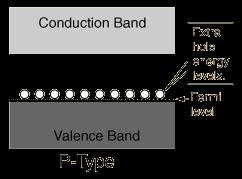
76 P type silicon. Replace a silicon atom with a group 3 atom such as aluminium.( 3 valence electrons) This lowers the number of electrons in the valence band which creates a hole in the structure. Electrons can move through the structure. This is called p type silicon. P is for positive as there is a deficiency of electrons.

77 N type Replace a silicon atom with a group 5 atom such as phosphorous ( 5 valence electrons ) The extra electron introduced here goes into the conduction band as the valence band is full. This is n type silicon. N for negative as additional electrons have been introduced into the structure.
78 Energy Band View of Semiconductors Conductors, semiconductors, insulators: Why is it that when individual atoms get close together to form a solid such as copper, silicon, or quartz they form materials that have a high, variable, or low ability to conduct current? Understand in terms of allowed, empty, and occupied electronic energy levels and electronic energy bands.
79 Fig. 1. Calculated energy levels in the diamond structure as a function of assumed atomic spacing at T = 0 o K. (From Introduction to Semiconductor Physics, Wiley, 1964)
80 In Fig. 1, at right atoms are essentially isolated; at left atomic separations are just a few tenths of a nanometer, characteristic of atoms in a silicon crystal. If we start with N atoms of silicon at the right, which have 14 electrons each, there must be 14N allowed energy levels for the electrons. (You learned about this in physics in connection with the Bohr atom, the Pauli Exclusion principle, etc.) If the atoms are pushed together to form a solid chunk of silicon, the electrons of neighboring atoms will interact and the allowed energy levels will broaden into energy bands.
81 When the actual spacing is reached, the quantummechanical calculation results are that: At lowest energies very narrow ranges of energy are allowed for inner electrons (these are core electrons, near the nuclei); A higher band of 4N allowed states exists that, at 0 o K, is filled with 4N electrons; Then an energy gap, E G, appears with no allowed states (no electrons permitted!); and At highest energies a band of allowed states appears that is entirely empty at 0 o K. Can this crystal conduct electricity?
82 NO, it cannot conductor electricity at 0 o K because that involves moving charges and therefore an increase of electron energy but we have only two bands of states separated by a forbidden energy gap, E G. The (lower) valence band is entirely filled, and the (upper) conduction band states are entirely empty. To conduct electricity we need to have a band that has some filled states (some electrons!) and some empty states that can be occupied by electrons whose energies increase.
83 Fig. 2 shows the situation at 0 o K for (left) a metallic solid such as copper, and (right) a semiconductor such as silicon. The metal can conduct at 0 o K because the uppermost band contains some electrons and some empty available energy states. The semiconductor cannot conduct it is an insulator. If we raise the temperature of the semiconductor, some electrons in the filled valence band may pick up enough energy to jump up into an unoccupied state in the conduction band. Thus, at a finite temperature, a pure (intrinsic) semiconductor has a finite electrical conductivity.
84 Fig. 2. Electronic energy bands for (a) metallic conductor at T = 0 o K; (b) insulator or intrinsic semiconductor at 0 o K.
85 How much conductivity can a pure (intrinsic) semiconductor exhibit? This depends on how much thermal energy there is and the size of the energy gap, E G : Mean thermal energy is kt, where k = Boltzmann s constant = 1.38 x J/K and T is the absolute temperature. In electron volts this is kt/qe, or 26 millivolts for room temperature (300 o K) For silicon, E G = 1.12 ev at 300 o K This leads in pure (intrinsic) Si to a carrier concentration n i = carriers/cm 3 at 300 o K
86 Adding Impurities (Doping) to Adjust Carrier Concentrations Adjust carrier concentrations locally in semiconductor by adding easily ionized impurities to produce mobile electrons and/or holes To make silicon N-type: Add valence 5 phosphorous (P) atoms to valence 4 silicon. Fifth electron is easily freed from the atom by a little thermal energy (0.045 ev for phosphorous) to create (donate) a mobile electron. Fig. 3a shows the donor energy level just below bottom of conduction band. To make silicon P-type: Add valence 3 boron (B) to silicon. An electron at the top of the valence band can pick up enough thermal energy to release it from the silicon so it attaches to a boron atom, completing its outer ring of electrons. In the band picture, Fig. 3b, this is represented by an acceptor. energy level ev above the top of the valence band.
87 Fig. 3a. Electronic energy band for n-type semiconductor (Ge) with donors only.
88 Fig. 3b. Electronic energy band for p-type semiconductor (Ge) with acceptors only.

89 Energy Bands Bloch Functions Nearly Free Electron Model Kronig-Penney Model Wave Equation of Electron in a Periodic Potential Number of Orbitals in a Band

90 Some successes of the free electron model: C, κ, σ, χ, Some failures of the free electron model: Distinction between metals, semimetals, semiconductors & insulators. Positive values of Hall coefficent. Relation between conduction & valence electrons. Magnetotransport. Band model New concepts: Effective mass Holes finite T impuritie s
91 Nearly Free Electron Model Bragg reflection no wave-like solutions energy gap Bragg condition: 2 2 k G k 2k G G 0 k 1 2 G / / e e i x a i x a 2cos x/ a 2i sin x / a k a

92 Origin of the Energy Gap cos 2 / U x U x a 2cos x/ a 2isin x / a 4co 4sin 2 s / 2 x a x/ a a 2 2 a 2 4U 0 dx cos 2 x / a U 0 P.Ravindran, PHY075- Condensed Matter Physics, Spring : Energy Bands in Solids Eg dx U x E E
93 Bloch Functions Periodic potential Translational symmetry Abelian group T = {T(Rl)} Rr r R T 1 T R f r f T R r f r R k-representation of T(Rl) is i e kr l Basis = e i kr Corresponding basis function for the Schrodinger equation must satisfy T 1 i kr l Rl k r k T Rl r r R e k r k l i l or r R e kr r k l k This can be satisfied by the Bloch function k i r e kr ukr where u r R u r k l k i G l e R 1 representative values of k are contained inside the Brillouin zone.
 continuous: Ae Be b e ik ab Qb Qb ikab Ce De e ψ (0) continuous: ika ikb QC QD ika ika ψ (a) continuous: ikae ikbe b e i k ab Qb Qb ik ab QCe QDe")
94 Kronig-Penney Model 2 2 d U 2 x 2m dx U na b x na b a 1 0 U 0 n a b a x n a b 0 xa U 0 Ae ik x Be ik x K 2m 2 2 b x 0 U U 0 Ce Qx De Qx Bloch theorem: ψ(0) continuous: A B C D a x a b b x e 0 ik a b U 0 Q 2m 2 2 ika ika ψ(a) continuous: Ae Be b e ik ab Qb Qb ikab Ce De e ψ (0) continuous: ika ikb QC QD ika ika ψ (a) continuous: ikae ikbe b e i k ab Qb Qb ik ab QCe QDe e
95 A 0 ika ika Qbik ab Qbi k ab e e e e B 0 ik ik Q Q C 0 ika ika Qbi k ab Qbik ab ike ike Qe Qe D 0 Q K 2QK 2 2 sinh Qb sin Ka cosh Qb cos Ka cos k a b 1 2 Delta function potential: b 0, U0 such that Q ba P finite 2 Thus Q K, Qb 1 so that P Ka sin Ka cos Ka cos ka
96 K Ka in units of 2 2m 2ma P Ka sin Ka cos Ka cos ka P 3 2
97 H j j Matrix Mechanics E Ansatz r ci ir r c H E c j j j j j r H c E c i j j j i j j H i j E Si j c j 0 Hi j i H j i j i j j i 3 * A d r A S r r Matrix equation H E S c 0 Secular equation: HE S 0 Eigen-problem Orthonormal basis: Si j i j i j S I
98 Fourier Series of the Periodic Potential U r R Ur m l U r U Gm e m i G r R 3 l li ai i1 3 G m b a b 2 m i i i1 1 3 i 1 m n 3 i m n d x e G G r d x e mn G G r V V i j i j V = Volume of crystal volume of unit cell 1 m 3 i G r G r U m d x e U For a lattice with atomic basis at positions ρα in the unit cell r rρ U r ρ R U rρ U U i m i m r G U U e e m m G ρ G r m U G U G e l U i Gm G e i G ρ m m is the structural factor m m r
99 Plane Wave Expansion Bloch function r k r k V 1 i k e r V 1 i k r i Gm e m C e m r k Gm k Gn mn Cm r k Gm m V = Volume of crystal 2 k G 2 m k G H k G k G U k G 2m n m nm n m, k G k G G U G G U U n m p n p m p Matrix form of the Schrodinger equation: 2 2 k Gn E nm U Gn Gm Cm 0 m 2m n m n = 0: 2 2 E C0 U G mcm 0 P.Ravindran, PHY075-2mCondensed Matter m Physics, Spring 2013 : Energy Bands in Solids k (central equation)
100 Crystal Momentum of an Electron Properties of k: i e kr u k ikr l ikr i l r r r R e e u r R e kr r k k k l k l e i U = 0 k r kr Selection rules in collision processes crystal momentum of electron is k. Eq., phonon k q kg absorption:
101 Solution of the Central Equation m E U C 0 k G G G m nm n m m k k 2m D lattice, only U g U g U 0 k2g E U 0 0 C 2 0 U kg E U 0 C U k E U 0 C0 0 0 U E U C 0 kg U k2g E C2 0
102 Kronig-Penney Model in Reciprocal Space U x A x sa a/2 a a/2 s 2 U cosg x n n /2 1 a a a/2 n 1 Un dx U x cos Gnx dx A A (only s = 0 term contributes) a/2 1 1 dx cos G x cos G x a 2 a/2 m n mn Eigen-equation: m E A kg C 0 m nm m cot x n C 1 n x n A E k G 2 1 2mA 2mE 2 n k 2 a n m C m 1 n A E k G n 2K 2 n 2 n n k K k K a a n n E 2 A k 2m K 2 n a 2 2mE 2 a cot 1 cot 1 k K a k K a 4K 2 2
103 2 a 1 1 cot k K a cot k K a 2mA 4K 2 2 K 2mE 2 a 4K sin Ka 1 1 sin k K a sin k K a 2 2 cot a cot b sin a b sin asin b a sin Ka 2K cos ka cos Ka 2sin a sin b cos a b cos a b P Ka sin Ka cos Ka cos ka with P maa (Kronig-Penney model)

104 Empty Lattice Approximation Free electron in vacuum: Free electron in empty lattice: k k 2m 2 2 k G 2 2 k n k k kg k1 st BZ 2m Simple cubic
105 Approximate Solution Near a Zone Boundary m E U C 0 k G G G Weak U, λk2g >> U m nm n m m k k 2m 2 2 kg E U 0 C 1 0 U E U C 0 k 0 0 U k g E C 1 0 k near zone right boundary: k 1 2 k 0 g a kg E U C1 0 U E C kg k kg k E E U 0 k g U U C C C E k g for E near λk 1 E U kg k kg k
106 1 E k g k k g k U g 2 g K K 2 2 2m 2m kg k K m k g K 2 K << g/2 g g 2 g K K 2 2 2m 2m kg k 2 Kg m 2U Kg 4U 2U U m kg k 2 2 g/2 K 2U U 2m E 2m 2 2m U g K g/2 U 1 2
107 C C 1 0 C k g C C k C 0 1 x C e C e ik x 0 1 i kg x

108 Number of Orbitals in a Band Linear crystal of length L composed of of N cells of lattice L Na constant a. ik x Periodic boundary x L x e u x condition: 2 n 2 n k L 2 n k N inequivalent values L Na of k Generalization to 3-D crystals: Number of k points in 1st BZ = Number of primitive cells Each primitive cell contributes one k point to each band. Crystals with odd numbers of electrons in primitive cell must be metals, e.g., alkali & noble metals metal semi-metal insulator


109 Braggs Law of Diffraction 2dsin(0)=nl d=spacing of parallel atomic planes 0=angle of incidence l=wavelength of incident beam Requires l<=2d Bragg reflection of electron waves in crystals cause energy gap. At locations of Bragg reflection solution to the Schrödinger equation do not exist.


110 Brillouin Zone Defined as the primitive zone in reciprocal lattice Made up of all the wave vectors that satisfy the diffraction condition Wave vectors outside of Brillouin zone do not lead to solution of the Schrödinger Equation

111 Origin of Energy Gap In one dimension, solution to the Schrödinger equation at the boundaries of Brillouin are standing waves. Standing waves made up of equal parts of left and right moving waves Waves traveling in different directions have different energy, corresponding to energy gap
112 Band Gap zone boundary
113 + Origin of the Band Gap To get a standing wave at the boundaries, you can take a linear combination of two plane waves: a x i ikx a x i ikx e e e e / 2 / 1 a x e e a x i a x i 2cos / / 2 1 / / sin i x a i x a x e e i a

114 Origin of the Band Gap Electron Density

115 Origin of the Band Gap
116 Summary Band Structures What is being plotted? Energy vs. k, where k is the wavevector that gives the phase of the AO s as well as the wavelength of the electron wavefunction (crystal momentum). How many lines are there in a band structure diagram? As many as there are orbitals in the unit cell. How is the center of gravity energy level of each band determined? Usually follows from the MO diagram. How do we determine whether a band runs uphill or downhill? By comparing the orbital overlap at k=0 and k=/a. How do we distinguish metals from semiconductors and insulators? The Fermi level cuts a band in a metal, whereas there is a gap between the filled and empty states in a semiconductor. Why are some bands flat and others steep? This depends on the degree of orbital overlap between building units. Wide bands Large intermolecular overlap delocalized e - Narrow bands Weak intermolecular overlap localized e -
117 Energy Bands in Solids:
118 Bandstructure - Nomenclature For most purposes, it is sufficient to know the En(k) curves - the dispersion relations - along the major directions of the reciprocal lattice. This is exactly what is done when real band diagrams of crystals are shown. Directions are chosen that lead from the center of the Wigner- Seitz unit cell - or the Brillouin zones - to special symmetry points. These points are labeled according to the following rules: Points (and lines) inside the Brillouin zone are denoted with Greek letters. Points on the surface of the Brillouin zone with Roman letters. The center of the Wigner-Seitz cell is always denoted by a G
119 Bandstructure - Nomenclature For cubic reciprocal lattices, the points with a high symmetry on the Wigner- Seitz cell are the intersections of the Wigner Seitz cell with the low-indexed directions in the cubic elementary cell. simple cubic
120 BZ for fcc - Nomenclature We use the following nomenclature: (fcc): The intersection point with the [100] direction is called X (H) The line G X is called. The intersection point with the [110] direction is called K (N) The line G K is called S. The intersection point with the [111] direction is called L (P) The line G L is called L. Brillouin Zone for fcc is wigner seitz cell for bcc and vice versa.
121 Nomenclature BZ for bcc lattice We use the following nomenclature: (red for fcc, blue for bcc): The intersection point with the [100] direction is called X (H) The line G X is called. The intersection point with the [110] direction is called K (N) The line G K is called S. The intersection point with the [111] direction is called L (P) The line G L is called L.
122 Electron Energy Bands in 3D Real crystals are three-dimensional and we must consider their band structure in three dimensions, too. Of course, we must consider the reciprocal lattice, and, as always if we look at electronic properties, use the Wigner-Seitz cell (identical to the 1st Brillouin zone) as the unit cell. There is no way to express quantities that change as a function of three coordinates graphically, so we look at a two dimensional crystal first (which do exist in semiconductor and nanoscale physics). The qualitative recipe for obtaining the band structure of a two-dimensional lattice using the slightly adjusted parabolas of the free electron gas model is simple:
123 Electron Energy Bands in 3D The lower part (the "cup") is contained in the 1st Brillouin zone, the upper part (the "top") comes from the second BZ, but it is folded back into the first one. It thus would carry a different band index. This could be continued ad infinitum; but Brillouin zones with energies well above the Fermi energy are of no real interest. These are tracings along major directions. Evidently, they contain most of the relevant information in condensed form. It is clear that this structure has no band gap.
124 Band Structure: KCl We first depict the band structure of an ionic crystal, KCl. The bands are very narrow, almost like atomic ones. The band gap is large around 9 ev. For alkali halides they are generally in the range 7-14 ev.
125 Band Structure: silver (fcc)
126 Electron Density of States The electron density of states is a key parameter in the determination of the physical phenomena of solids. Knowing the energy levels, we can count how many energy levels are contained in an interval E at the energy E. This is best done in k - space. In phase space, a surface of constant energy is a sphere as schematically shown in the picture. Any "state", i.e. solution of the Schrodinger equation with a specific k, occupies the volume given by one of the little cubes in phase space. The number of cubes fitting inside the sphere at energy E thus is the number of all energy levels up to E.
127 Electron Density of States: Free Electrons Counting the number of cells (each containing one possible state of ) in an energy interval E, E + E thus correspond to taking the difference of the numbers of cubes contained in a sphere with "radius" E + E and of radius E. We thus obtain the density of states D(E) as DE ( ) 1 N( E, E E) N( E) V E 1 dn V de where N(E) is the number of states between E = 0 and E per volume unit; and V is the volume of the crystal.

128 Electron Density of States: Free Electrons The volume of the sphere in k-space is V 4 k 3 3 The volume Vk of one unit cell, containing two electron states is V k 2 L 3 The total number of states is then N V 4 k L k L V 3 k 38 P.Ravindran, PHY075- Condensed Matter Physics, Spring 2013 : Energy Bands in Solids 2
129 Electron Density of States: Free Electrons E 2 2 k 2mE k 2 2m N k L L 2mE / D( E) 1 dn 1 2m L de /2 E
130 Electron Density of States: Free Electrons D(E)
131 DOS in real Materials
132 Electron Density of States: If we know the band structure at every point in the Brillouin zone, then the DOS is given by the formula ds D( ) k 3 n 4 n 1 where the integral is over the surface Sn() is the surface in k space at which the n th eigenvalue has the value n. Obviously we can not evaluate this integral directly, since we don't know n(k) at all points; and we can only guess at the properties of its gradient. One common approximation is to use the tetrahedron method, which divides the Brillouin zone into (surprise) tetrahedra, and then linearly interpolate within the tetrahedra to determine the gradient. This method is an approximation, but its accuracy obviously improves as we increase the number of k-points.

133 Electron Density of States: ds D( ) k 3 n 4 n 1 When the denominator in the integral is zero, peaks due to van Hove singularities occur. Flat bands give rise to a high density of states. It is also higher close to the zone boundaries as illustrated for a two dimensional lattice below. Leon van Hove
134 Electron Density of States: Real Solids For the case of metals, the bands are very free electronlike (remember we compared with the empty lattice) and the conduction bands are partly filled. The figure shows the DOS for the cases of a metal, Cu, and a semiconductor Ge. Copper has a free electron-like s-band, upon which d-bands are superimposed. The peaks are due to the d-bands. For Ge the valence and conduction bands are clearly seen.
135 Electron Density of States The basic shape of the density of states versus energy is determined by an overlap of orbitals. In this case s and d orbitals fcc
136 Electron Density of States: bcc tungsten
Bonding in solids The interaction of electrons in neighboring atoms of a solid serves the very important function of holding the crystal together.
 Bonding in solids The interaction of electrons in neighboring atoms of a solid serves the very important function of holding the crystal together. For example Nacl In the Nacl lattice, each Na atom is
Three Most Important Topics (MIT) Today
 Today") Three Most Important Topics (MIT) Today Electrons in periodic potential Energy gap nearly free electron Bloch Theorem Energy gap tight binding Chapter 1 1 Electrons in Periodic Potential We now know the
Three Most Important Topics (MIT) Today Electrons in periodic potential Energy gap nearly free electron Bloch Theorem Energy gap tight binding Chapter 1 1 Electrons in Periodic Potential We now know the
Energy bands in solids. Some pictures are taken from Ashcroft and Mermin from Kittel from Mizutani and from several sources on the web.
 Energy bands in solids Some pictures are taken from Ashcroft and Mermin from Kittel from Mizutani and from several sources on the web. we are starting to remind p E = = mv 1 2 = k mv = 2 2 k 2m 2 Some
The potential is minimum at the positive ion sites and maximum between the two ions.
 1. Bloch theorem: - A crystalline solid consists of a lattice, which is composed of a large number of ion cores at regular intervals, and the conduction electrons that can move freely through out the lattice.
Electrons in a periodic potential
 Chapter 3 Electrons in a periodic potential 3.1 Bloch s theorem. We consider in this chapter electrons under the influence of a static, periodic potential V (x), i.e. such that it fulfills V (x) = V (x
Semiconductor Physics and Devices Chapter 3.
 Introduction to the Quantum Theory of Solids We applied quantum mechanics and Schrödinger s equation to determine the behavior of electrons in a potential. Important findings Semiconductor Physics and
Semiconductor Physics
 1 Semiconductor Physics 1.1 Introduction 2 1.2 The Band Theory of Solids 2 1.3 The Kronig Penney Model 3 1.4 The Bragg Model 8 1.5 Effective Mass 8 1.6 Number of States in a Band 10 1.7 Band Filling 12
7.4. Why we have two different types of materials: conductors and insulators?
 Phys463.nb 55 7.3.5. Folding, Reduced Brillouin zone and extended Brillouin zone for free particles without lattices In the presence of a lattice, we can also unfold the extended Brillouin zone to get
Mat E 272 Lecture 25: Electrical properties of materials
 Mat E 272 Lecture 25: Electrical properties of materials December 6, 2001 Introduction: Calcium and copper are both metals; Ca has a valence of +2 (2 electrons per atom) while Cu has a valence of +1 (1
ELEMENTARY BAND THEORY
 ELEMENTARY BAND THEORY PHYSICIST Solid state band Valence band, VB Conduction band, CB Fermi energy, E F Bloch orbital, delocalized n-doping p-doping Band gap, E g Direct band gap Indirect band gap Phonon
Nearly Free Electron Gas model - II
 Nearly Free Electron Gas model - II Contents 1 Lattice scattering 1 1.1 Bloch waves............................ 2 1.2 Band gap formation........................ 3 1.3 Electron group velocity and effective
Calculating Band Structure
 Calculating Band Structure Nearly free electron Assume plane wave solution for electrons Weak potential V(x) Brillouin zone edge Tight binding method Electrons in local atomic states (bound states) Interatomic
From Last Time Important new Quantum Mechanical Concepts. Atoms and Molecules. Today. Symmetry. Simple molecules.
 Today From Last Time Important new Quantum Mechanical Concepts Indistinguishability: Symmetries of the wavefunction: Symmetric and Antisymmetric Pauli exclusion principle: only one fermion per state Spin
Chapter 4: Bonding in Solids and Electronic Properties. Free electron theory
 Chapter 4: Bonding in Solids and Electronic Properties Free electron theory Consider free electrons in a metal an electron gas. regards a metal as a box in which electrons are free to move. assumes nuclei
Electrons in a weak periodic potential
 Electrons in a weak periodic potential Assumptions: 1. Static defect-free lattice perfectly periodic potential. 2. Weak potential perturbative effect on the free electron states. Perfect periodicity of
Section 10 Metals: Electron Dynamics and Fermi Surfaces
 Electron dynamics Section 10 Metals: Electron Dynamics and Fermi Surfaces The next important subject we address is electron dynamics in metals. Our consideration will be based on a semiclassical model.
7. FREE ELECTRON THEORY.
 7. FREE ELECTRON THEORY. Aim: To introduce the free electron model for the physical properties of metals. It is the simplest theory for these materials, but still gives a very good description of many
Electronic Structure Theory for Periodic Systems: The Concepts. Christian Ratsch
 Electronic Structure Theory for Periodic Systems: The Concepts Christian Ratsch Institute for Pure and Applied Mathematics and Department of Mathematics, UCLA Motivation There are 10 20 atoms in 1 mm 3
Solid State Physics. Lecture 10 Band Theory. Professor Stephen Sweeney
 Solid State Physics Lecture 10 Band Theory Professor Stephen Sweeney Advanced Technology Institute and Department of Physics University of Surrey, Guildford, GU2 7XH, UK s.sweeney@surrey.ac.uk Recap from
Minimal Update of Solid State Physics
 Minimal Update of Solid State Physics It is expected that participants are acquainted with basics of solid state physics. Therefore here we will refresh only those aspects, which are absolutely necessary
Nearly Free Electron Gas model - I
 Nearly Free Electron Gas model - I Contents 1 Free electron gas model summary 1 2 Electron effective mass 3 2.1 FEG model for sodium...................... 4 3 Nearly free electron model 5 3.1 Primitive
Introduction to Engineering Materials ENGR2000. Dr.Coates
 Introduction to Engineering Materials ENGR2000 Chapter 18: Electrical Properties Dr.Coates 18.2 Ohm s Law V = IR where R is the resistance of the material, V is the voltage and I is the current. l R A
Introduction to Semiconductor Physics. Prof.P. Ravindran, Department of Physics, Central University of Tamil Nadu, India
 Introduction to Semiconductor Physics 1 Prof.P. Ravindran, Department of Physics, Central University of Tamil Nadu, India http://folk.uio.no/ravi/cmp2013 Review of Semiconductor Physics Semiconductor fundamentals
Lecture 4: Basic elements of band theory
 Phys 769 Selected Topics in Condensed Matter Physics Summer 010 Lecture 4: Basic elements of band theory Lecturer: Anthony J. Leggett TA: Bill Coish 1 Introduction Most matter, in particular most insulating
5 Problems Chapter 5: Electrons Subject to a Periodic Potential Band Theory of Solids
 E n = :75, so E cont = E E n = :75 = :479. Using E =!, :479 = m e k z =! j e j m e k z! k z = r :479 je j m e = :55 9 (44) (v g ) z = @! @k z = m e k z = m e :55 9 = :95 5 m/s. 4.. A ev electron is to
Electro - Principles I
 Electro - Principles I Page 10-1 Atomic Theory It is necessary to know what goes on at the atomic level of a semiconductor so the characteristics of the semiconductor can be understood. In many cases a
PHYSICS 4750 Physics of Modern Materials Chapter 5: The Band Theory of Solids
 PHYSICS 4750 Physics of Modern Materials Chapter 5: The Band Theory of Solids 1. Introduction We have seen that when the electrons in two hydrogen atoms interact, their energy levels will split, i.e.,
Unit III Free Electron Theory Engineering Physics
 . Introduction The electron theory of metals aims to explain the structure and properties of solids through their electronic structure. The electron theory is applicable to all solids i.e., both metals
CHAPTER 2: ENERGY BANDS & CARRIER CONCENTRATION IN THERMAL EQUILIBRIUM. M.N.A. Halif & S.N. Sabki
 CHAPTER 2: ENERGY BANDS & CARRIER CONCENTRATION IN THERMAL EQUILIBRIUM OUTLINE 2.1 INTRODUCTION: 2.1.1 Semiconductor Materials 2.1.2 Basic Crystal Structure 2.1.3 Basic Crystal Growth technique 2.1.4 Valence
Introduction to Condensed Matter Physics
 Introduction to Condensed Matter Physics The Reciprocal Lattice M.P. Vaughan Overview Overview of the reciprocal lattice Periodic functions Reciprocal lattice vectors Bloch functions k-space Dispersion
Physics 541: Condensed Matter Physics
 Physics 541: Condensed Matter Physics Final Exam Monday, December 17, 2012 / 14:00 17:00 / CCIS 4-285 Student s Name: Instructions There are 24 questions. You should attempt all of them. Mark your response
FREQUENTLY ASKED QUESTIONS February 21, 2017
 FREQUENTLY ASKED QUESTIONS February 21, 2017 Content Questions How do you place a single arsenic atom with the ratio 1 in 100 million? Sounds difficult to get evenly spread throughout. Yes, techniques
Physics 221A Fall 1996 Notes 16 Bloch s Theorem and Band Structure in One Dimension
 Physics 221A Fall 1996 Notes 16 Bloch s Theorem and Band Structure in One Dimension In these notes we examine Bloch s theorem and band structure in problems with periodic potentials, as a part of our survey
Note that it is traditional to draw the diagram for semiconductors rotated 90 degrees, i.e. the version on the right above.
 5 Semiconductors The nearly free electron model applies equally in the case where the Fermi level lies within a small band gap (semiconductors), as it does when the Fermi level lies within a band (metal)
The electronic structure of solids. Charge transport in solids
 The electronic structure of solids We need a picture of the electronic structure of solid that we can use to explain experimental observations and make predictions Why is diamond an insulator? Why is sodium
Chap 7 Non-interacting electrons in a periodic potential
 Chap 7 Non-interacting electrons in a periodic potential Bloch theorem The central equation Brillouin zone Rotational symmetry Dept of Phys M.C. Chang Bloch recalled, The main problem was to explain how
Quantum Condensed Matter Physics Lecture 5
 Quantum Condensed Matter Physics Lecture 5 detector sample X-ray source monochromator David Ritchie http://www.sp.phy.cam.ac.uk/drp2/home QCMP Lent/Easter 2019 5.1 Quantum Condensed Matter Physics 1. Classical
Microscopic Ohm s Law
 Microscopic Ohm s Law Outline Semiconductor Review Electron Scattering and Effective Mass Microscopic Derivation of Ohm s Law 1 TRUE / FALSE 1. Judging from the filled bands, material A is an insulator.
ECE 340 Lecture 6 : Intrinsic and Extrinsic Material I Class Outline:
 ECE 340 Lecture 6 : Intrinsic and Extrinsic Material I Class Outline: Effective Mass Intrinsic Material Extrinsic Material Things you should know when you leave Key Questions What is the physical meaning
Communications with Optical Fibers
 Communications with Optical Fibers In digital communications, signals are generally sent as light pulses along an optical fiber. Information is first converted to an electrical signal in the form of pulses
Chapter Two. Energy Bands and Effective Mass
 Chapter Two Energy Bands and Effective Mass Energy Bands Formation At Low Temperature At Room Temperature Valence Band Insulators Metals Effective Mass Energy-Momentum Diagrams Direct and Indirect Semiconduction
Problem Sheet 1 From material in Lectures 2 to 5
 lectrons in Solids ) Problem Sheet From material in Lectures to 5 ) [Standard derivation] Consider the free electron model for a - dimensional solid between x = and x = L. For this model the time independent
sin[( t 2 Home Problem Set #1 Due : September 10 (Wed), 2008
, 2008") Home Problem Set #1 Due : September 10 (Wed), 008 1. Answer the following questions related to the wave-particle duality. (a) When an electron (mass m) is moving with the velocity of υ, what is the wave
Home Problem Set #1 Due : September 10 (Wed), 008 1. Answer the following questions related to the wave-particle duality. (a) When an electron (mass m) is moving with the velocity of υ, what is the wave
Ch. 2: Energy Bands And Charge Carriers In Semiconductors
 Ch. 2: Energy Bands And Charge Carriers In Semiconductors Discrete energy levels arise from balance of attraction force between electrons and nucleus and repulsion force between electrons each electron
Review of Semiconductor Physics
 Solid-state physics Review of Semiconductor Physics The daunting task of solid state physics Quantum mechanics gives us the fundamental equation The equation is only analytically solvable for a handful
Review of Optical Properties of Materials
 Review of Optical Properties of Materials Review of optics Absorption in semiconductors: qualitative discussion Derivation of Optical Absorption Coefficient in Direct Semiconductors Photons When dealing
Chapter 1 Overview of Semiconductor Materials and Physics
 Chapter 1 Overview of Semiconductor Materials and Physics Professor Paul K. Chu Conductivity / Resistivity of Insulators, Semiconductors, and Conductors Semiconductor Elements Period II III IV V VI 2 B
半導體元件與物理. Semiconductor Devices and physics 許正興國立聯合大學電機工程學系 聯大電機系電子材料與元件應用實驗室
 半導體元件與物理 Semiconductor Devices and physics 許正興國立聯合大學電機工程學系 1. Crystal Structure of Solids 2. Quantum Theory of Solids 3. Semiconductor in Equilibrium and Carrier Transport phenomena 4. PN Junction and
Chapter 3: Introduction to the Quantum Theory of Solids
 Chapter 3: Introduction to the Quantum Theory of Solids Determine the properties of electrons in a crystal lattice. Determine the statistical characteristics of the very large number of electrons in a
Free Electron Model for Metals
 Free Electron Model for Metals Metals are very good at conducting both heat and electricity. A lattice of in a sea of electrons shared between all nuclei (moving freely between them): This is referred
Lecture. Ref. Ihn Ch. 3, Yu&Cardona Ch. 2
 Lecture Review of quantum mechanics, statistical physics, and solid state Band structure of materials Semiconductor band structure Semiconductor nanostructures Ref. Ihn Ch. 3, Yu&Cardona Ch. 2 Reminder
Crystal Properties. MS415 Lec. 2. High performance, high current. ZnO. GaN
 Crystal Properties Crystal Lattices: Periodic arrangement of atoms Repeated unit cells (solid-state) Stuffing atoms into unit cells Determine mechanical & electrical properties High performance, high current
Charge Carriers in Semiconductor
 Charge Carriers in Semiconductor To understand PN junction s IV characteristics, it is important to understand charge carriers behavior in solids, how to modify carrier densities, and different mechanisms
PHYS485 Materials Physics
 5/11/017 PHYS485 Materials Physics Dr. Gregory W. Clar Manchester University LET S GO ON A (TEK)ADVENTURE! WHAT? TRIP TO A MAKER S SPACE IN FORT WAYNE WHEN? THURSDAY, MAY 11 TH @ 5PM WHERE? TEKVENTURE
In chapter 3, when we discussed metallic bonding, the primary attribute was that electrons are delocalized.
 Lecture 15: free electron gas Up to this point we have not discussed electrons explicitly, but electrons are the first offenders for most useful phenomena in materials. When we distinguish between metals,
EE 346: Semiconductor Devices
 EE 346: Semiconductor Devices Lecture - 5 02/01/2017 Tewodros A. Zewde 1 The One-Electron Atom The potential function is due to the coulomb attraction between the proton and electron and is given by where
Experimental Determination of Crystal Structure
 Experimental Determination of Crystal Structure Branislav K. Nikolić Department of Physics and Astronomy, University of Delaware, U.S.A. PHYS 624: Introduction to Solid State Physics http://www.physics.udel.edu/~bnikolic/teaching/phys624/phys624.html
Basic cell design. Si cell
 Basic cell design Si cell 1 Concepts needed to describe photovoltaic device 1. energy bands in semiconductors: from bonds to bands 2. free carriers: holes and electrons, doping 3. electron and hole current:
Electrons in Crystals. Chris J. Pickard
 Electrons in Crystals Chris J. Pickard Electrons in Crystals The electrons in a crystal experience a potential with the periodicity of the Bravais lattice: U(r + R) = U(r) The scale of the periodicity
Lecture 3: Electron statistics in a solid
 Lecture 3: Electron statistics in a solid Contents Density of states. DOS in a 3D uniform solid.................... 3.2 DOS for a 2D solid........................ 4.3 DOS for a D solid........................
Atoms? All matters on earth made of atoms (made up of elements or combination of elements).
.") Chapter 1 Atoms? All matters on earth made of atoms (made up of elements or combination of elements). Atomic Structure Atom is the smallest particle of an element that can exist in a stable or independent
Chapter 1 Atoms? All matters on earth made of atoms (made up of elements or combination of elements). Atomic Structure Atom is the smallest particle of an element that can exist in a stable or independent
Semiconductor physics I. The Crystal Structure of Solids
 Lecture 3 Semiconductor physics I The Crystal Structure of Solids 1 Semiconductor materials Types of solids Space lattices Atomic Bonding Imperfection and doping in SOLIDS 2 Semiconductor Semiconductors
Lecture 14 The Free Electron Gas: Density of States
 Lecture 4 The Free Electron Gas: Density of States Today:. Spin.. Fermionic nature of electrons. 3. Understanding the properties of metals: the free electron model and the role of Pauli s exclusion principle.
Resistance (R) Temperature (T)
 Temperature (T)") CHAPTER 1 Physical Properties of Elements and Semiconductors 1.1 Introduction Semiconductors constitute a large class of substances which have resistivities lying between those of insulators and conductors.
CHAPTER 1 Physical Properties of Elements and Semiconductors 1.1 Introduction Semiconductors constitute a large class of substances which have resistivities lying between those of insulators and conductors.
Lecture 2 Electrons and Holes in Semiconductors
 EE 471: Transport Phenomena in Solid State Devices Spring 2018 Lecture 2 Electrons and Holes in Semiconductors Bryan Ackland Department of Electrical and Computer Engineering Stevens Institute of Technology
Introduction to Quantum Theory of Solids
 Lecture 5 Semiconductor physics III Introduction to Quantum Theory of Solids 1 Goals To determine the properties of electrons in a crystal lattice To determine the statistical characteristics of the very
SEMICONDUCTOR PHYSICS
 SEMICONDUCTOR PHYSICS by Dibyendu Chowdhury Semiconductors The materials whose electrical conductivity lies between those of conductors and insulators, are known as semiconductors. Silicon Germanium Cadmium
Free Electron Model for Metals
 Free Electron Model for Metals Metals are very good at conducting both heat and electricity. A lattice of in a sea of electrons shared between all nuclei (moving freely between them): This is referred
ELECTRONS IN A PERIODIC POTENTIAL AND ENERGY BANDS IN SOLIDS-2
 ELECTRONS IN A PERIODIC POTENTIAL AND ENERGY BANDS IN SOLIDS-2 ENERGY BANDS IN A SOLID : A FORMAL APPROACH SCHROEDINGER'S EQUATION FOR A PERIODIC POTENTIAL * Electrons motion in a crystal will now be considered
DO PHYSICS ONLINE ELECTRIC CURRENT FROM IDEAS TO IMPLEMENTATION ATOMS TO TRANSISTORS ELECTRICAL PROPERTIES OF SOLIDS
 DO PHYSICS ONLINE FROM IDEAS TO IMPLEMENTATION 9.4.3 ATOMS TO TRANSISTORS ELECTRICAL PROPERTIES OF SOLIDS ELECTRIC CURRENT Different substances vary considerably in their electrical properties. It is a
Semiconductors. Semiconductors also can collect and generate photons, so they are important in optoelectronic or photonic applications.
 Semiconductors Semiconducting materials have electrical properties that fall between true conductors, (like metals) which are always highly conducting and insulators (like glass or plastic or common ceramics)
Engineering 2000 Chapter 8 Semiconductors. ENG2000: R.I. Hornsey Semi: 1
 Engineering 2000 Chapter 8 Semiconductors ENG2000: R.I. Hornsey Semi: 1 Overview We need to know the electrical properties of Si To do this, we must also draw on some of the physical properties and we
Due to the quantum nature of electrons, one energy state can be occupied only by one electron.
 In crystalline solids, not all values of the electron energy are possible. The allowed intervals of energy are called allowed bands (shown as blue and chess-board blue). The forbidden intervals are called
Kronig-Penney model. 2m dx. Solutions can be found in region I and region II Match boundary conditions
 Kronig-Penney model I II d V( x) m dx E Solutions can be found in region I and region II Match boundary conditions Linear differential equations with periodic coefficients Have exponentially decaying solutions,
ELEC311( 물리전자, Physical Electronics) Course Outlines:
 Course Outlines:") ELEC311( 물리전자, Physical Electronics) Course Outlines: by Professor Jung-Hee Lee Lecture notes are prepared with PPT and available before the class (http://abeek.knu.ac.kr). The topics in the notes are
ELEC311( 물리전자, Physical Electronics) Course Outlines: by Professor Jung-Hee Lee Lecture notes are prepared with PPT and available before the class (http://abeek.knu.ac.kr). The topics in the notes are
FYS Vår 2017 (Kondenserte fasers fysikk)
") FYS3410 - Vår 2017 (Kondenserte fasers fysikk) http://www.uio.no/studier/emner/matnat/fys/fys3410/v16/index.html Pensum: Introduction to Solid State Physics by Charles Kittel (Chapters 1-9, 11, 17, 18,
FYS3410 - Vår 2017 (Kondenserte fasers fysikk) http://www.uio.no/studier/emner/matnat/fys/fys3410/v16/index.html Pensum: Introduction to Solid State Physics by Charles Kittel (Chapters 1-9, 11, 17, 18,
EE 346: Semiconductor Devices
 EE 346: Semiconductor Devices Lecture - 6 02/06/2017 Tewodros A. Zewde 1 DENSTY OF STATES FUNCTON Since current is due to the flow of charge, an important step in the process is to determine the number
ENERGY BANDS AND GAPS IN SEMICONDUCTOR. Muhammad Hafeez Javed
 ENERGY BANDS AND GAPS IN SEMICONDUCTOR Muhammad Hafeez Javed www.rmhjaved.com rmhjaved@gmail.com Out Line Introduction Energy band Classification of materials Direct and indirect band gap of SC Classification
STM spectroscopy (STS)
") STM spectroscopy (STS) di dv 4 e ( E ev, r) ( E ) M S F T F Basic concepts of STS. With the feedback circuit open the variation of the tunneling current due to the application of a small oscillating voltage
STM spectroscopy (STS) di dv 4 e ( E ev, r) ( E ) M S F T F Basic concepts of STS. With the feedback circuit open the variation of the tunneling current due to the application of a small oscillating voltage
Electrical Properties
 Electrical Properties Electrical Conduction R Ohm s law V = IR I l Area, A V where I is current (Ampere), V is voltage (Volts) and R is the resistance (Ohms or ) of the conductor Resistivity Resistivity,
Electronic Devices & Circuits
 Electronic Devices & Circuits For Electronics & Communication Engineering By www.thegateacademy.com Syllabus Syllabus for Electronic Devices Energy Bands in Intrinsic and Extrinsic Silicon, Carrier Transport,
Semiconductors 1. Explain different types of semiconductors in detail with necessary bond diagrams. Intrinsic semiconductors:
 Semiconductors 1. Explain different types of semiconductors in detail with necessary bond diagrams. There are two types of semi conductors. 1. Intrinsic semiconductors 2. Extrinsic semiconductors Intrinsic
Chapter 4: Summary. Solve lattice vibration equation of one atom/unitcellcase Consider a set of ions M separated by a distance a,
 Chapter 4: Summary Solve lattice vibration equation of one atom/unitcellcase case. Consider a set of ions M separated by a distance a, R na for integral n. Let u( na) be the displacement. Assuming only
Solid State Device Fundamentals
 Solid State Device Fundamentals ES 345 Lecture Course by Alexander M. Zaitsev alexander.zaitsev@csi.cuny.edu Tel: 718 982 2812 Oice 4101b 1 The ree electron model o metals The ree electron model o metals
Electron levels in a periodic potential: general remarks. Daniele Toffoli January 11, / 46
 Electron levels in a periodic potential: general remarks Daniele Toffoli January 11, 2017 1 / 46 Outline 1 Mathematical tools 2 The periodic potential 3 Bloch s theorem and Born-von Karman boundary conditions
Electronic Structure of Surfaces
 Electronic Structure of Surfaces When solids made of an infinite number of atoms are formed, it is a common misconception to consider each atom individually. Rather, we must consider the structure of the
Metals: the Drude and Sommerfeld models p. 1 Introduction p. 1 What do we know about metals? p. 1 The Drude model p. 2 Assumptions p.
 Metals: the Drude and Sommerfeld models p. 1 Introduction p. 1 What do we know about metals? p. 1 The Drude model p. 2 Assumptions p. 2 The relaxation-time approximation p. 3 The failure of the Drude model
Chapter 6 Free Electron Fermi Gas
 Chapter 6 Free Electron Fermi Gas Free electron model: The valence electrons of the constituent atoms become conduction electrons and move about freely through the volume of the metal. The simplest metals
Lecture 2: Background dconcepts
 Optoelectronics I Lecture : Background dconcepts M. Soroosh Assistant Professor of Electronics Shahid Chamran University 1 Face Centered Crystal (FCC) Body Centered Crystal (BCC) Bragg s Law William Lawrence
LN 3 IDLE MIND SOLUTIONS
 IDLE MIND SOLUTIONS 1. Let us first look in most general terms at the optical properties of solids with band gaps (E g ) of less than 4 ev, semiconductors by definition. The band gap energy (E g ) can
PART 1 Introduction to Theory of Solids
 Elsevier UK Job code: MIOC Ch01-I044647 9-3-2007 3:03p.m. Page:1 Trim:165 240MM TS: Integra, India PART 1 Introduction to Theory of Solids Elsevier UK Job code: MIOC Ch01-I044647 9-3-2007 3:03p.m. Page:2
Solids. properties & structure
 Solids properties & structure Determining Crystal Structure crystalline solids have a very regular geometric arrangement of their particles the arrangement of the particles and distances between them is
2) Atom manipulation. Xe / Ni(110) Model: Experiment:
 Atom manipulation. Xe / Ni(110) Model: Experiment:") 2) Atom manipulation D. Eigler & E. Schweizer, Nature 344, 524 (1990) Xe / Ni(110) Model: Experiment: G.Meyer, et al. Applied Physics A 68, 125 (1999) First the tip is approached close to the adsorbate
2) Atom manipulation D. Eigler & E. Schweizer, Nature 344, 524 (1990) Xe / Ni(110) Model: Experiment: G.Meyer, et al. Applied Physics A 68, 125 (1999) First the tip is approached close to the adsorbate
Electrons in periodic potential
 Chapter 9 Electrons in periodic potential The computation of electronic states in a solid is a nontrivial problem. A great simplification can be achieved if the solid is a crystal, i.e. if it can be described
Probability and Normalization
 Probability and Normalization Although we don t know exactly where the particle might be inside the box, we know that it has to be in the box. This means that, ψ ( x) dx = 1 (normalization condition) L
Quantum Condensed Matter Physics
 QCMP-2017/18 Problem sheet 2: Quantum Condensed Matter Physics Band structure 1. Optical absorption of simple metals Sketch the typical energy-wavevector dependence, or dispersion relation, of electrons
Carriers Concentration in Semiconductors - V. Prof.P. Ravindran, Department of Physics, Central University of Tamil Nadu, India
 Carriers Concentration in Semiconductors - V 1 Prof.P. Ravindran, Department of Physics, Central University of Tamil Nadu, India http://folk.uio.no/ravi/semi2013 Motion and Recombination of Electrons and
Electronic structure of correlated electron systems. Lecture 2
 Electronic structure of correlated electron systems Lecture 2 Band Structure approach vs atomic Band structure Delocalized Bloch states Fill up states with electrons starting from the lowest energy No
DFT EXERCISES. FELIPE CERVANTES SODI January 2006
 DFT EXERCISES FELIPE CERVANTES SODI January 2006 http://www.csanyi.net/wiki/space/dftexercises Dr. Gábor Csányi 1 Hydrogen atom Place a single H atom in the middle of a largish unit cell (start with a
1 Review of semiconductor materials and physics
 Part One Devices 1 Review of semiconductor materials and physics 1.1 Executive summary Semiconductor devices are fabricated using specific materials that offer the desired physical properties. There are