Due to the quantum nature of electrons, one energy state can be occupied only by one electron.
|
|
|
- Simon Rodgers
- 5 years ago
- Views:
Transcription
1
2
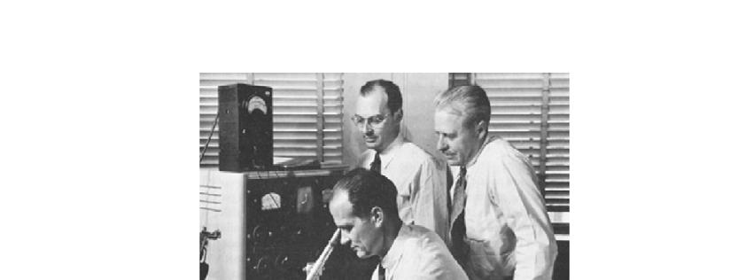
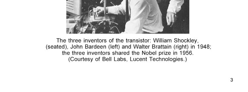
3
 (the white strip between the blue strips). Due to the quantum nature of electrons, one energy state can be occupied only by one electron.")
4 In crystalline solids, not all values of the electron energy are possible. The allowed intervals of energy are called allowed bands (shown as blue and chess-board blue). The forbidden intervals are called forbidden bands (or gaps) (the white strip between the blue strips). Due to the quantum nature of electrons, one energy state can be occupied only by one electron. At T = 0, the electrons occupy the states with the lowest possible energies. The energy up to which the states are occupied is called Fermi energy (Fermi level) and is denoted E F. Thus, at T = 0, the probability to find an electron in a state of energy E (distribution function of the electrons) is a step function centred at E F. In semiconductors, the number of electrons is just enough to completely fill a certain amount of allowed bands. So that in this case, at T = 0, one has only completely filled bands and absolutely empty allowed bands. The highest filled band is called valence band. The lowest empty band is called conduction band. At a finite temperature, the distribution function of electrons has the shape of a smeared step function. It is called Fermi - Dirac function. It is centred at E F which have the meaning of the energy at which the probability to find an electron is ½. At finite temperatures, due to the smearing of the distribution function there are some electrons in the conduction bands and there are some empty places (holes) in the valence band.
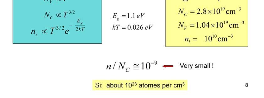
5 In a typical situation in semiconductors, the number of electrons in the conduction band is much smaller that the total amount of the available places. Thus, in the conduction band, all the electrons have energies which are very close to that of the bottom of this band E C. The density of electrons in the conduction band at a finite temperature can be calculated as the product: the probability to have a electron in a state with the energy E C times the number of available states per unit volume. The latter variable is called density of states. All holes are concentrated at the top of the valence band. They represent missing electrons of the energy corresponding to the top of this band E V. The number of holes is calculated as the number of missing electrons. As mentioned, the number of electrons in the conduction band and holes in the valence band is typically much smaller than the total amount of places in these band. Mathematically that means that the Fermi level is never too close neither to E V nor to E C so that E C E F >>kt and E F -E V >> kt. At room temperature kt = ev. ev is an energy unit equal to the energy that an electron acquires when passing a potential difference of 1 V. Typically in semiconductors E C E v is about 1 V.
6 A change of the Fermi level, E F, leads to a variation in the concentrations of the electrons and holes, n and p, however, the product np does not depend on E F. This makes the mass action law. The mass action law holds only when the concentrations of the electrons and holes correspond to the equilibrium distribution functions. It holds with a good accuracy as far as the Fermi level is not too close to the conduction or valence band which is usually the case.

7 Intrinsic semiconductor is a pure semiconductor which is absolutely stoichiometric and contains no impurities.
8

9 In intrinsic semiconductors, the Fermi level is very close to the middle of the forbidden gap.

10 Substitution of some atoms of the semiconductor with atoms of other elements influences the amount of electrons and holes in the system. A substitution with an element having a more positive valence brings extra electrons. The substitution actually brings new states in the forbidden gap with electrons sitting on these. If these states are close enough to E C, the new electrons readily go to the conduction band. A doping donor atom is typically positive charged since it has given an electron to the conduction band. Such a substitution is called donor doping.
.")
11 In donor doped semiconductors, the concentration of electrons in the conduction band, n, is much greater than that of intrinsic semiconductors, n i. The increase of n results in a strong reduction of the hole concentration, p (due to the mass action law). When a donor-impurity atom looses electrons (ionized impurity), it becomes positively charged. From the electroneutrality condition: the charge of electrons = the charge of ionized impurities (the charge of holes in this case is much smaller than that of the electrons and can be neglected). This increase of n with doping means that the Fermi level moves closer to E C.
12 A substitution with an element having a less positive valence brings about new states in the forbidden band. If these states are close enough to the valence band, they are readily occupied by electrons from this band. These electrons, when leaving the valence band, create extra holes in it. A doping acceptor atom is typically negatively charged since it has received an electron from the valence band. Such a substitution is called acceptor doping.
.")
13 In the case of acceptor doped semiconductor, the hole concentration in the valence band, p, is much greater than that in the intrinsic semiconductor, n i. The increase of p results in a strong reduction of the concentration of n (due to the mass action law). Every acceptor-impurity atom with an electron sitting on it (ionized impurity) becomes negatively charged. Thus, the electroneutrality condition becomes: the charge of holes = the charge of ionized impurities (the charge of electrons being neglected). This increase of p with doping corresponds to a shift of the Fermi level towards to E V.


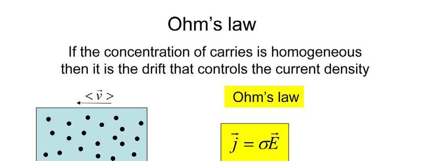
14 If the valence band is completely filled, no electric transport is possible in the system, since there are no empty places with energies close to those of the available electrons. Since, one place can be occupied only by one electron, without these empty places none of the electrons can change its state and no motion in the system is possible. For this reason, the electrical transport in semiconductors is possible only due to a small amount of electrons in the conduction band and a small amount of empty places (holes) in the valence band. Electric field, E, acting on the negative charge of an electron causes its movement in the opposite direction. A constant field corresponds to a force applied to the electron but, due to scattering against thermally vibrating host atoms and impurities, the electron does not accelerate but rather moves with a constant velocity. This regime of motion is called drift and the corresponding velocity drift velocity. If the electron concentration is inhomogeneous in space, the thermal motion tries to make it homogeneous. This leads to a motion of electrons called diffusion. The flux of electrons (number of electrons crossing an element of surface per second divided by the area of the element) is controlled by the gradient of electron concentration. The ratio drift velocity/field is called mobility,.( In the absence of the concentration gradient.) The ratio flux/concentration gradient is called diffusion coefficient, D. ( In the absence of the electric field.) The mobility and diffusion coefficients obey the Einstein relation. All these logic equally applies to holes. They can be considered as particles with a positive charge and a positive mass. These notions can be rationalized as follows: Under an electric field the electrons in the valence band move on average in the direction opposite to that of the field. This corresponds to a motion of the empty places (holes) in the direction of the field as expected from positively charged particles with positive mass.
15
16

17 Strictly speaking, the amount of electrons in the conduction band is not fixed in time, rather it is fixed only on average. The electrons come to and go from the valence band. Actually any electron stays in the conduction band only during some typical times called electron life time, e. For the time intervals shorter than e, the electrons in the conduction band can be treated as normal particles which do not appear and diaper all the time. The same logic holds for the holes. The hole life time, h, is the typical time during which a hole can move in the valence band before it is filled by an electron coming to the valence band from the conduction band or from an impurity. The process of annihilation of an electron from the conduction band and a hole from the valence band is called recombination. In doped semiconductors, due to the mass action law, either n << p or p << n. That implies the terminology: majority carries and minority carriers. Since one electron and one hole participate in the recombination, the impact of the recombination is essential only on minority carriers. When an electron and a hole recombine, the electron loses the energy equal to E g. This energy is not lost. It can be transformed into light or heart. In the former case, a quantum of light - photon appears, with the energy equal to that lost by the electron.

18 Extra electrons can be brought to the conduction band with an electric current. At the same time holes form in the valence band. Electron-hole pairs can also be created by light. This phenomenon is called generation. Under illumination with photons (quanta of light), whose energies exceeded the width of the forbidden gap, the concentrations of electrons and holes differ form their equilibrium values.
.")

19 Once the concentration of carries is changed compared to its equilibrium value, it tries to return back to is. It mainly returns back during the life time of particles (electrons or holes). During this time, the added particles diffuse away from the place where they were created. The distance on which they typically manage to diffuse during their lifetime is called diffusion length.
ESE 372 / Spring 2013 / Lecture 5 Metal Oxide Semiconductor Field Effect Transistor
 Metal Oxide Semiconductor Field Effect Transistor V G V G 1 Metal Oxide Semiconductor Field Effect Transistor We will need to understand how this current flows through Si What is electric current? 2 Back
Semiconductor Physics. Lecture 3
 Semiconductor Physics Lecture 3 Intrinsic carrier density Intrinsic carrier density Law of mass action Valid also if we add an impurity which either donates extra electrons or holes the number of carriers
n N D n p = n i p N A
 Summary of electron and hole concentration in semiconductors Intrinsic semiconductor: E G n kt i = pi = N e 2 0 Donor-doped semiconductor: n N D where N D is the concentration of donor impurity Acceptor-doped
In this block the two transport mechanisms will be discussed: diffusion and drift.
 ET3034TUx - 2.3.3 Transport of charge carriers What are the charge carrier transport principles? In this block the two transport mechanisms will be discussed: diffusion and drift. We will discuss that
Lecture 1. OUTLINE Basic Semiconductor Physics. Reading: Chapter 2.1. Semiconductors Intrinsic (undoped) silicon Doping Carrier concentrations
 silicon Doping Carrier concentrations") Lecture 1 OUTLINE Basic Semiconductor Physics Semiconductors Intrinsic (undoped) silicon Doping Carrier concentrations Reading: Chapter 2.1 EE105 Fall 2007 Lecture 1, Slide 1 What is a Semiconductor? Low
Lecture 1 OUTLINE Basic Semiconductor Physics Semiconductors Intrinsic (undoped) silicon Doping Carrier concentrations Reading: Chapter 2.1 EE105 Fall 2007 Lecture 1, Slide 1 What is a Semiconductor? Low
Carriers Concentration and Current in Semiconductors
 Carriers Concentration and Current in Semiconductors Carrier Transport Two driving forces for carrier transport: electric field and spatial variation of the carrier concentration. Both driving forces lead
EECS130 Integrated Circuit Devices
 EECS130 Integrated Circuit Devices Professor Ali Javey 8/30/2007 Semiconductor Fundamentals Lecture 2 Read: Chapters 1 and 2 Last Lecture: Energy Band Diagram Conduction band E c E g Band gap E v Valence
3.1 Introduction to Semiconductors. Y. Baghzouz ECE Department UNLV
 3.1 Introduction to Semiconductors Y. Baghzouz ECE Department UNLV Introduction In this lecture, we will cover the basic aspects of semiconductor materials, and the physical mechanisms which are at the
ECE 606 Homework Week 7 Mark Lundstrom Purdue University (revised 2/25/13) e E i! E T
 e E i! E T") ECE 606 Homework Week 7 Mark Lundstrom Purdue University (revised 2/25/13) 1) Consider an n- type semiconductor for which the only states in the bandgap are donor levels (i.e. ( E T = E D ). Begin with
ECE 606 Homework Week 7 Mark Lundstrom Purdue University (revised 2/25/13) 1) Consider an n- type semiconductor for which the only states in the bandgap are donor levels (i.e. ( E T = E D ). Begin with
Lecture 15: Optoelectronic devices: Introduction
 Lecture 15: Optoelectronic devices: Introduction Contents 1 Optical absorption 1 1.1 Absorption coefficient....................... 2 2 Optical recombination 5 3 Recombination and carrier lifetime 6 3.1
Semiconductor Physics
 Semiconductor Physics Motivation Is it possible that there might be current flowing in a conductor (or a semiconductor) even when there is no potential difference supplied across its ends? Look at the
The photovoltaic effect occurs in semiconductors where there are distinct valence and
 How a Photovoltaic Cell Works The photovoltaic effect occurs in semiconductors where there are distinct valence and conduction bands. (There are energies at which electrons can not exist within the solid)
Semiconductor Detectors
 Semiconductor Detectors Summary of Last Lecture Band structure in Solids: Conduction band Conduction band thermal conductivity: E g > 5 ev Valence band Insulator Charge carrier in conductor: e - Charge
Session 5: Solid State Physics. Charge Mobility Drift Diffusion Recombination-Generation
 Session 5: Solid State Physics Charge Mobility Drift Diffusion Recombination-Generation 1 Outline A B C D E F G H I J 2 Mobile Charge Carriers in Semiconductors Three primary types of carrier action occur
Ch. 2: Energy Bands And Charge Carriers In Semiconductors
 Ch. 2: Energy Bands And Charge Carriers In Semiconductors Discrete energy levels arise from balance of attraction force between electrons and nucleus and repulsion force between electrons each electron
Lecture 2. Semiconductor Physics. Sunday 4/10/2015 Semiconductor Physics 1-1
 Lecture 2 Semiconductor Physics Sunday 4/10/2015 Semiconductor Physics 1-1 Outline Intrinsic bond model: electrons and holes Charge carrier generation and recombination Intrinsic semiconductor Doping:
smal band gap Saturday, April 9, 2011
 small band gap upper (conduction) band empty small gap valence band filled 2s 2p 2s 2p hybrid (s+p)band 2p no gap 2s (depend on the crystallographic orientation) extrinsic semiconductor semi-metal electron
Semiconductors 1. Explain different types of semiconductors in detail with necessary bond diagrams. Intrinsic semiconductors:
 Semiconductors 1. Explain different types of semiconductors in detail with necessary bond diagrams. There are two types of semi conductors. 1. Intrinsic semiconductors 2. Extrinsic semiconductors Intrinsic
Density of states for electrons and holes. Distribution function. Conduction and valence bands
 Intrinsic Semiconductors In the field of semiconductors electrons and holes are usually referred to as free carriers, or simply carriers, because it is these particles which are responsible for carrying
This is the 15th lecture of this course in which we begin a new topic, Excess Carriers. This topic will be covered in two lectures.
 Solid State Devices Dr. S. Karmalkar Department of Electronics and Communication Engineering Indian Institute of Technology, Madras Lecture - 15 Excess Carriers This is the 15th lecture of this course
Chapter 1 Overview of Semiconductor Materials and Physics
 Chapter 1 Overview of Semiconductor Materials and Physics Professor Paul K. Chu Conductivity / Resistivity of Insulators, Semiconductors, and Conductors Semiconductor Elements Period II III IV V VI 2 B
Note that it is traditional to draw the diagram for semiconductors rotated 90 degrees, i.e. the version on the right above.
 5 Semiconductors The nearly free electron model applies equally in the case where the Fermi level lies within a small band gap (semiconductors), as it does when the Fermi level lies within a band (metal)
CLASS 12th. Semiconductors
 CLASS 12th Semiconductors 01. Distinction Between Metals, Insulators and Semi-Conductors Metals are good conductors of electricity, insulators do not conduct electricity, while the semiconductors have
Basic Semiconductor Physics
 6 Basic Semiconductor Physics 6.1 Introduction With this chapter we start with the discussion of some important concepts from semiconductor physics, which are required to understand the operation of solar
Charge Carriers in Semiconductor
 Charge Carriers in Semiconductor To understand PN junction s IV characteristics, it is important to understand charge carriers behavior in solids, how to modify carrier densities, and different mechanisms
ECE 250 Electronic Devices 1. Electronic Device Modeling
 ECE 250 Electronic Devices 1 ECE 250 Electronic Device Modeling ECE 250 Electronic Devices 2 Introduction to Semiconductor Physics You should really take a semiconductor device physics course. We can only
Qualitative Picture of the Ideal Diode. G.R. Tynan UC San Diego MAE 119 Lecture Notes
 Qualitative Picture of the Ideal Diode G.R. Tynan UC San Diego MAE 119 Lecture Notes Band Theory of Solids: From Single Attoms to Solid Crystals Isolated Li atom (conducting metal) Has well-defined, isolated
Mat E 272 Lecture 25: Electrical properties of materials
 Mat E 272 Lecture 25: Electrical properties of materials December 6, 2001 Introduction: Calcium and copper are both metals; Ca has a valence of +2 (2 electrons per atom) while Cu has a valence of +1 (1
Semiconductor Devices and Circuits Fall Midterm Exam. Instructor: Dr. Dietmar Knipp, Professor of Electrical Engineering. Name: Mat. -Nr.
 Semiconductor Devices and Circuits Fall 2003 Midterm Exam Instructor: Dr. Dietmar Knipp, Professor of Electrical Engineering Name: Mat. -Nr.: Guidelines: Duration of the Midterm: 1 hour The exam is a closed
collisions of electrons. In semiconductor, in certain temperature ranges the conductivity increases rapidly by increasing temperature
 1.9. Temperature Dependence of Semiconductor Conductivity Such dependence is one most important in semiconductor. In metals, Conductivity decreases by increasing temperature due to greater frequency of
Introduction to Engineering Materials ENGR2000. Dr.Coates
 Introduction to Engineering Materials ENGR2000 Chapter 18: Electrical Properties Dr.Coates 18.2 Ohm s Law V = IR where R is the resistance of the material, V is the voltage and I is the current. l R A
Effective masses in semiconductors
 Effective masses in semiconductors The effective mass is defined as: In a solid, the electron (hole) effective mass represents how electrons move in an applied field. The effective mass reflects the inverse
ECE 442. Spring, Lecture -2
 ECE 442 Power Semiconductor Devices and Integrated circuits Spring, 2006 University of Illinois at Chicago Lecture -2 Semiconductor physics band structures and charge carriers 1. What are the types of
Engineering 2000 Chapter 8 Semiconductors. ENG2000: R.I. Hornsey Semi: 1
 Engineering 2000 Chapter 8 Semiconductors ENG2000: R.I. Hornsey Semi: 1 Overview We need to know the electrical properties of Si To do this, we must also draw on some of the physical properties and we
EE143 Fall 2016 Microfabrication Technologies. Evolution of Devices
 EE143 Fall 2016 Microfabrication Technologies Prof. Ming C. Wu wu@eecs.berkeley.edu 511 Sutardja Dai Hall (SDH) 1-1 Evolution of Devices Yesterday s Transistor (1947) Today s Transistor (2006) 1-2 1 Why
Electrical Resistance
 Electrical Resistance I + V _ W Material with resistivity ρ t L Resistance R V I = L ρ Wt (Unit: ohms) where ρ is the electrical resistivity 1 Adding parts/billion to parts/thousand of dopants to pure
Classification of Solids
 Classification of Solids Classification by conductivity, which is related to the band structure: (Filled bands are shown dark; D(E) = Density of states) Class Electron Density Density of States D(E) Examples
EE 346: Semiconductor Devices. 02/08/2017 Tewodros A. Zewde 1
 EE 346: Semiconductor Devices 02/08/2017 Tewodros A. Zewde 1 DOPANT ATOMS AND ENERGY LEVELS Without help the total number of carriers (electrons and holes) is limited to 2ni. For most materials, this is
PN Junction
 P Junction 2017-05-04 Definition Power Electronics = semiconductor switches are used Analogue amplifier = high power loss 250 200 u x 150 100 u Udc i 50 0 0 50 100 150 200 250 300 350 400 i,u dc i,u u
Carriers Concentration in Semiconductors - V. Prof.P. Ravindran, Department of Physics, Central University of Tamil Nadu, India
 Carriers Concentration in Semiconductors - V 1 Prof.P. Ravindran, Department of Physics, Central University of Tamil Nadu, India http://folk.uio.no/ravi/semi2013 Motion and Recombination of Electrons and
SEMICONDUCTOR PHYSICS
 SEMICONDUCTOR PHYSICS by Dibyendu Chowdhury Semiconductors The materials whose electrical conductivity lies between those of conductors and insulators, are known as semiconductors. Silicon Germanium Cadmium
Semiconductor Device Physics
 1 Semiconductor Device Physics Lecture 3 http://zitompul.wordpress.com 2 0 1 3 Semiconductor Device Physics 2 Three primary types of carrier action occur inside a semiconductor: Drift: charged particle
EE 446/646 Photovoltaic Devices I. Y. Baghzouz
 EE 446/646 Photovoltaic Devices I Y. Baghzouz What is Photovoltaics? First used in about 1890, the word has two parts: photo, derived from the Greek word for light, volt, relating to electricity pioneer
The German University in Cairo. Faculty of Information Engineering & Technology Semiconductors (Elct 503) Electronics Department Fall 2014
 Electronics Department Fall 2014") The German University in Cairo th Electronics 5 Semester Faculty of Information Engineering & Technology Semiconductors (Elct 503) Electronics Department Fall 2014 Problem Set 3 1- a) Find the resistivity
The German University in Cairo th Electronics 5 Semester Faculty of Information Engineering & Technology Semiconductors (Elct 503) Electronics Department Fall 2014 Problem Set 3 1- a) Find the resistivity
Population inversion occurs when there are more atoms in the excited state than in the ground state. This is achieved through the following:
 Lasers and SemiconductorsTutorial Lasers 1. Fill in the table the differences between spontaneous emission and stimulated emission in atoms: External stimulus Direction of emission Phase & coherence of
ECE 440 Lecture 20 : PN Junction Electrostatics II Class Outline:
 ECE 440 Lecture 20 : PN Junction Electrostatics II Class Outline: Depletion Approximation Step Junction Things you should know when you leave Key Questions What is the space charge region? What are the
PHYS208 P-N Junction. Olav Torheim. May 30, 2007
 1 PHYS208 P-N Junction Olav Torheim May 30, 2007 1 Intrinsic semiconductors The lower end of the conduction band is a parabola, just like in the quadratic free electron case (E = h2 k 2 2m ). The density
The Meaning of Fermi-Level And Related Concepts (Like Band-Bending)
") The Meaning of Fermi-Level And Related Concepts (Like Band-Bending) Martin Peckerar January 14, 2003 The Fermi level is a term derived from statistical mechanics and used to calculate the number of mobile
The Meaning of Fermi-Level And Related Concepts (Like Band-Bending) Martin Peckerar January 14, 2003 The Fermi level is a term derived from statistical mechanics and used to calculate the number of mobile
Semiconductor physics I. The Crystal Structure of Solids
 Lecture 3 Semiconductor physics I The Crystal Structure of Solids 1 Semiconductor materials Types of solids Space lattices Atomic Bonding Imperfection and doping in SOLIDS 2 Semiconductor Semiconductors
Lecture 2 Electrons and Holes in Semiconductors
 EE 471: Transport Phenomena in Solid State Devices Spring 2018 Lecture 2 Electrons and Holes in Semiconductors Bryan Ackland Department of Electrical and Computer Engineering Stevens Institute of Technology
Chemistry Instrumental Analysis Lecture 8. Chem 4631
 Chemistry 4631 Instrumental Analysis Lecture 8 UV to IR Components of Optical Basic components of spectroscopic instruments: stable source of radiant energy transparent container to hold sample device
pn JUNCTION THE SHOCKLEY MODEL
 The pn Junction: The Shockley Model ( S. O. Kasap, 1990-001) 1 pn JUNCTION THE SHOCKLEY MODEL Safa Kasap Department of Electrical Engineering University of Saskatchewan Canada Although the hole and its
Topic 11-3: Fermi Levels of Intrinsic Semiconductors with Effective Mass in Temperature
 Topic 11-3: Fermi Levels of Intrinsic Semiconductors with Effective Mass in Temperature Summary: In this video we aim to get an expression for carrier concentration in an intrinsic semiconductor. To do
Lecture 7: Extrinsic semiconductors - Fermi level
 Lecture 7: Extrinsic semiconductors - Fermi level Contents 1 Dopant materials 1 2 E F in extrinsic semiconductors 5 3 Temperature dependence of carrier concentration 6 3.1 Low temperature regime (T < T
ET3034TUx Utilization of band gap energy
 ET3034TUx - 3.3.1 - Utilization of band gap energy In the last two weeks we have discussed the working principle of a solar cell and the external parameters that define the performance of a solar cell.
EECS143 Microfabrication Technology
 EECS143 Microfabrication Technology Professor Ali Javey Introduction to Materials Lecture 1 Evolution of Devices Yesterday s Transistor (1947) Today s Transistor (2006) Why Semiconductors? Conductors e.g
KATIHAL FİZİĞİ MNT-510
 KATIHAL FİZİĞİ MNT-510 YARIİLETKENLER Kaynaklar: Katıhal Fiziği, Prof. Dr. Mustafa Dikici, Seçkin Yayıncılık Katıhal Fiziği, Şakir Aydoğan, Nobel Yayıncılık, Physics for Computer Science Students: With
Chapter Two. Energy Bands and Effective Mass
 Chapter Two Energy Bands and Effective Mass Energy Bands Formation At Low Temperature At Room Temperature Valence Band Insulators Metals Effective Mass Energy-Momentum Diagrams Direct and Indirect Semiconduction
Minimal Update of Solid State Physics
 Minimal Update of Solid State Physics It is expected that participants are acquainted with basics of solid state physics. Therefore here we will refresh only those aspects, which are absolutely necessary
EE301 Electronics I , Fall
 EE301 Electronics I 2018-2019, Fall 1. Introduction to Microelectronics (1 Week/3 Hrs.) Introduction, Historical Background, Basic Consepts 2. Rewiev of Semiconductors (1 Week/3 Hrs.) Semiconductor materials
Bohr s Model, Energy Bands, Electrons and Holes
 Dual Character of Material Particles Experimental physics before 1900 demonstrated that most of the physical phenomena can be explained by Newton's equation of motion of material particles or bodies and
Current mechanisms Exam January 27, 2012
 Current mechanisms Exam January 27, 2012 There are four mechanisms that typically cause currents to flow: thermionic emission, diffusion, drift, and tunneling. Explain briefly which kind of current mechanisms
5. Semiconductors and P-N junction
 5. Semiconductors and P-N junction Thomas Zimmer, University of Bordeaux, France Summary Learning Outcomes... 2 Physical background of semiconductors... 2 The silicon crystal... 2 The energy bands... 3
Electronics The basics of semiconductor physics
 Electronics The basics of semiconductor physics Prof. Márta Rencz, Gergely Nagy BME DED September 16, 2013 The basic properties of semiconductors Semiconductors conductance is between that of conductors
Basic cell design. Si cell
 Basic cell design Si cell 1 Concepts needed to describe photovoltaic device 1. energy bands in semiconductors: from bonds to bands 2. free carriers: holes and electrons, doping 3. electron and hole current:
ECE 142: Electronic Circuits Lecture 3: Semiconductors
 Faculty of Engineering ECE 142: Electronic Circuits Lecture 3: Semiconductors Agenda Intrinsic Semiconductors Extrinsic Semiconductors N-type P-type Carrier Transport Drift Diffusion Semiconductors A semiconductor
CLASS 1 & 2 REVISION ON SEMICONDUCTOR PHYSICS. Reference: Electronic Devices by Floyd
 CLASS 1 & 2 REVISION ON SEMICONDUCTOR PHYSICS Reference: Electronic Devices by Floyd 1 ELECTRONIC DEVICES Diodes, transistors and integrated circuits (IC) are typical devices in electronic circuits. All
The Semiconductor in Equilibrium
 Lecture 6 Semiconductor physics IV The Semiconductor in Equilibrium Equilibrium, or thermal equilibrium No external forces such as voltages, electric fields. Magnetic fields, or temperature gradients are
UNIVERSITY OF CALIFORNIA College of Engineering Department of Electrical Engineering and Computer Sciences. Professor Ali Javey. Spring 2009.
 UNIVERSITY OF CALIFORNIA College of Engineering Department of Electrical Engineering and Computer Sciences EE143 Professor Ali Javey Spring 2009 Exam 1 Name: SID: Closed book. One sheet of notes is allowed.
Unit IV Semiconductors Engineering Physics
 Introduction A semiconductor is a material that has a resistivity lies between that of a conductor and an insulator. The conductivity of a semiconductor material can be varied under an external electrical
Doped Semiconductors *
 OpenStax-CNX module: m1002 1 Doped Semiconductors * Bill Wilson This work is produced by OpenStax-CNX and licensed under the Creative Commons Attribution License 1.0 To see how we can make silicon a useful
CME 300 Properties of Materials. ANSWERS: Homework 9 November 26, As atoms approach each other in the solid state the quantized energy states:
 CME 300 Properties of Materials ANSWERS: Homework 9 November 26, 2011 As atoms approach each other in the solid state the quantized energy states: are split. This splitting is associated with the wave
Introduction to Semiconductor Physics. Prof.P. Ravindran, Department of Physics, Central University of Tamil Nadu, India
 Introduction to Semiconductor Physics 1 Prof.P. Ravindran, Department of Physics, Central University of Tamil Nadu, India http://folk.uio.no/ravi/cmp2013 Review of Semiconductor Physics Semiconductor fundamentals
electronics fundamentals
 electronics fundamentals circuits, devices, and applications THOMAS L. FLOYD DAVID M. BUCHLA Lesson 1: Diodes and Applications Semiconductors Figure 1-1 The Bohr model of an atom showing electrons in orbits
DO PHYSICS ONLINE ELECTRIC CURRENT FROM IDEAS TO IMPLEMENTATION ATOMS TO TRANSISTORS ELECTRICAL PROPERTIES OF SOLIDS
 DO PHYSICS ONLINE FROM IDEAS TO IMPLEMENTATION 9.4.3 ATOMS TO TRANSISTORS ELECTRICAL PROPERTIES OF SOLIDS ELECTRIC CURRENT Different substances vary considerably in their electrical properties. It is a
Electronic Devices & Circuits
 Electronic Devices & Circuits For Electronics & Communication Engineering By www.thegateacademy.com Syllabus Syllabus for Electronic Devices Energy Bands in Intrinsic and Extrinsic Silicon, Carrier Transport,
Variation of Energy Bands with Alloy Composition E
 Variation of Energy Bands with Alloy Composition E 3.0 E.8.6 L 0.3eV Al x GaAs AlAs 1- xas 1.43eV.16eV X k.4 L. X.0 X 1.8 L 1.6 1.4 0 0. 0.4 0.6 X 0.8 1 1 Carriers in intrinsic Semiconductors Ec 4º 1º
ECE 335: Electronic Engineering Lecture 2: Semiconductors
 Faculty of Engineering ECE 335: Electronic Engineering Lecture 2: Semiconductors Agenda Intrinsic Semiconductors Extrinsic Semiconductors N-type P-type Carrier Transport Drift Diffusion Semiconductors
Crystal Properties. MS415 Lec. 2. High performance, high current. ZnO. GaN
 Crystal Properties Crystal Lattices: Periodic arrangement of atoms Repeated unit cells (solid-state) Stuffing atoms into unit cells Determine mechanical & electrical properties High performance, high current
PHYS208 p-n junction. January 15, 2010
 1 PHYS208 p-n junction January 15, 2010 List of topics (1) Density of states Fermi-Dirac distribution Law of mass action Doped semiconductors Dopinglevel p-n-junctions 1 Intrinsic semiconductors List of
Carrier Recombination
 Notes for ECE-606: Spring 013 Carrier Recombination Professor Mark Lundstrom Electrical and Computer Engineering Purdue University, West Lafayette, IN USA lundstro@purdue.edu /19/13 1 carrier recombination-generation
Lecture 3 Semiconductor Physics (II) Carrier Transport
 Carrier Transport") Lecture 3 Semiconductor Physics (II) Carrier Transport Thermal Motion Carrier Drift Carrier Diffusion Outline Reading Assignment: Howe and Sodini; Chapter 2, Sect. 2.4-2.6 6.012 Spring 2009 Lecture 3 1
Lecture 3 Semiconductor Physics (II) Carrier Transport Thermal Motion Carrier Drift Carrier Diffusion Outline Reading Assignment: Howe and Sodini; Chapter 2, Sect. 2.4-2.6 6.012 Spring 2009 Lecture 3 1
Semiconductor Physics fall 2012 problems
 Semiconductor Physics fall 2012 problems 1. An n-type sample of silicon has a uniform density N D = 10 16 atoms cm -3 of arsenic, and a p-type silicon sample has N A = 10 15 atoms cm -3 of boron. For each
Lecture 4. Density of States and Fermi Energy Concepts. Reading: (Cont d) Pierret
 Pierret") C 3040 Dr. Alan Doolittle Lecture 4 Density of States and Fermi nergy Concepts Reading: (Cont d Pierret 2.1-2.6 C 3040 Dr. Alan Doolittle Density of States Concept Quantum Mechanics tells us that the number
C 3040 Dr. Alan Doolittle Lecture 4 Density of States and Fermi nergy Concepts Reading: (Cont d Pierret 2.1-2.6 C 3040 Dr. Alan Doolittle Density of States Concept Quantum Mechanics tells us that the number
Introduction into defect studies. in ceramic materials(iii) Structure, Defects and Defect Chemistry. Z. Wang. January 18, 2002
 Structure, Defects and Defect Chemistry. Z. Wang. January 18, 2002") Introduction into defect studies in ceramic materials(iii) Structure, Defects and Defect Chemistry Z. Wang January 18, 2002 1. Mass, Charge and Site Balance The Schottky reactions for NaCl and MgO, respectively,
Introduction into defect studies in ceramic materials(iii) Structure, Defects and Defect Chemistry Z. Wang January 18, 2002 1. Mass, Charge and Site Balance The Schottky reactions for NaCl and MgO, respectively,
Lecture 17: Semiconductors - continued (Kittel Ch. 8)
") Lecture 17: Semiconductors - continued (Kittel Ch. 8) Fermi nergy Conduction Band All bands have the form - const 2 near the band edge Valence Bands X = (2,,) π/a L = (1,1,1) π/a Physics 46 F 26 Lect 17
Lecture 17: Semiconductors - continued (Kittel Ch. 8) Fermi nergy Conduction Band All bands have the form - const 2 near the band edge Valence Bands X = (2,,) π/a L = (1,1,1) π/a Physics 46 F 26 Lect 17
EE 346: Semiconductor Devices
 EE 346: Semiconductor Devices Lecture - 6 02/06/2017 Tewodros A. Zewde 1 DENSTY OF STATES FUNCTON Since current is due to the flow of charge, an important step in the process is to determine the number
EE495/695 Introduction to Semiconductors I. Y. Baghzouz ECE Department UNLV
 EE495/695 Introduction to Semiconductors I Y. Baghzouz ECE Department UNLV Introduction Solar cells have always been aligned closely with other electronic devices. We will cover the basic aspects of semiconductor
Lecture 8. Equations of State, Equilibrium and Einstein Relationships and Generation/Recombination
 Lecture 8 Equations of State, Equilibrium and Einstein Relationships and Generation/Recombination Reading: (Cont d) Notes and Anderson 2 sections 3.4-3.11 Energy Equilibrium Concept Consider a non-uniformly
First-Hand Investigation: Modeling of Semiconductors
 perform an investigation to model the behaviour of semiconductors, including the creation of a hole or positive charge on the atom that has lost the electron and the movement of electrons and holes in
Chapter 7. The pn Junction
 Chapter 7 The pn Junction Chapter 7 PN Junction PN junction can be fabricated by implanting or diffusing donors into a P-type substrate such that a layer of semiconductor is converted into N type. Converting
Lecture 3b. Bonding Model and Dopants. Reading: (Cont d) Notes and Anderson 2 sections
 Notes and Anderson 2 sections") Lecture 3b Bonding Model and Dopants Reading: (Cont d) Notes and Anderson 2 sections 2.3-2.7 The need for more control over carrier concentration Without help the total number of carriers (electrons and
Lecture 3b Bonding Model and Dopants Reading: (Cont d) Notes and Anderson 2 sections 2.3-2.7 The need for more control over carrier concentration Without help the total number of carriers (electrons and
Semiconductor Physics and Devices
 The pn Junction 1) Charge carriers crossing the junction. 3) Barrier potential Semiconductor Physics and Devices Chapter 8. The pn Junction Diode 2) Formation of positive and negative ions. 4) Formation
Unit III Free Electron Theory Engineering Physics
 . Introduction The electron theory of metals aims to explain the structure and properties of solids through their electronic structure. The electron theory is applicable to all solids i.e., both metals
Atoms? All matters on earth made of atoms (made up of elements or combination of elements).
.") Chapter 1 Atoms? All matters on earth made of atoms (made up of elements or combination of elements). Atomic Structure Atom is the smallest particle of an element that can exist in a stable or independent
Chapter 1 Atoms? All matters on earth made of atoms (made up of elements or combination of elements). Atomic Structure Atom is the smallest particle of an element that can exist in a stable or independent
Energetic particles and their detection in situ (particle detectors) Part II. George Gloeckler
 Part II. George Gloeckler") Energetic particles and their detection in situ (particle detectors) Part II George Gloeckler University of Michigan, Ann Arbor, MI University of Maryland, College Park, MD Simple particle detectors Gas-filled
Energetic particles and their detection in situ (particle detectors) Part II George Gloeckler University of Michigan, Ann Arbor, MI University of Maryland, College Park, MD Simple particle detectors Gas-filled
Calculating Band Structure
 Calculating Band Structure Nearly free electron Assume plane wave solution for electrons Weak potential V(x) Brillouin zone edge Tight binding method Electrons in local atomic states (bound states) Interatomic
Course overview. Me: Dr Luke Wilson. The course: Physics and applications of semiconductors. Office: E17 open door policy
 Course overview Me: Dr Luke Wilson Office: E17 open door policy email: luke.wilson@sheffield.ac.uk The course: Physics and applications of semiconductors 10 lectures aim is to allow time for at least one
1. Introduction of solid state 1.1. Elements of solid state physics:
 1. Introduction of solid state 1.1. Elements of solid state physics: To understand the operation of many of the semiconductor devices we need, at least, an appreciation of the solid state physics of homogeneous
THE UNIVERSITY OF NEW SOUTH WALES SCHOOL OF PHYSICS FINAL EXAMINATION JUNE/JULY PHYS3080 Solid State Physics
 THE UNIVERSITY OF NEW SOUTH WALES SCHOOL OF PHYSICS FINAL EXAMINATION JUNE/JULY 006 PHYS3080 Solid State Physics Time Allowed hours Total number of questions - 5 Answer ALL questions All questions are