Photonic and phononic crystal research at Sandia
|
|
|
- Verity Hawkins
- 5 years ago
- Views:
Transcription


1 Photonic and phononic crystal research at Sandia Sandia National Laboratories and University of New Mexico T.S. Willie Luk and Ihab El-Kady Quantum, Molecular and High Performance Modeling and Simulation for Devices and Systems (QMHP) April 16-17, 2007 Arlington, VA Sandia is a multiprogram laboratory operated by Sandia Corporation, a Lockheed Martin Company, for the United States Department of Energy s National Nuclear Security Administration under contract DE-AC04-94AL
2 Outline Sandia missions, capabilities and interests. Recent work in photonic and phononic crystals 2


3 Sandia s Institutional Resources Information Assurance & Survivability Assessment Analysis 3
4 Supports Sandia's role as a "Science-Based Engineering" Laboratory NNSA Science and Technology Thrust Physical and chemical understanding of NW component operation, aging, failure mechanisms, and response to radiation exposure. Collective Hierarchical Systems Thrust The study and simulation of dynamic self-assembly processes and cooperative behaviors in living systems. Compound Semiconductor Science and Technology Thrust Advancing semiconductor research in areas such as quantum phenomena, defect physics, materials and device modeling, and heteroepitaxy. Nanosciences Explore phenomena that are new and unique at the nanometer length scale, and develop bridges from the nanometer length scale to longer scales. Optical Sciences We emphasize innovative work in laser development, nonlinear optics, spectroscopy, remote sensing, and photon - material interactions. 4

5 96,000-square-foot CINT Core Facility will be a distribution point for researchers best served at smaller gateways at LANL and Sandia $75.8 million Center one of five funded nationwide by the Office of Science Nano-bio-micro Interfaces: Import biological principles and functions into artificial bio-mimetic nano- - and microsystems. Nanophotonics and Nanelectronics: Precise control of electronic and photonic wavefunctions to invoke novel and unique properties. Complex Functional Nanomaterials: Promote complex and collective interactions between individual components in materials to yield emergent properties and functions. Nanomechanics: Understanding the underlying mechanisms of mechanical behavior of nanoscale materials and structures is the objective of the nanomechanics theme. 5

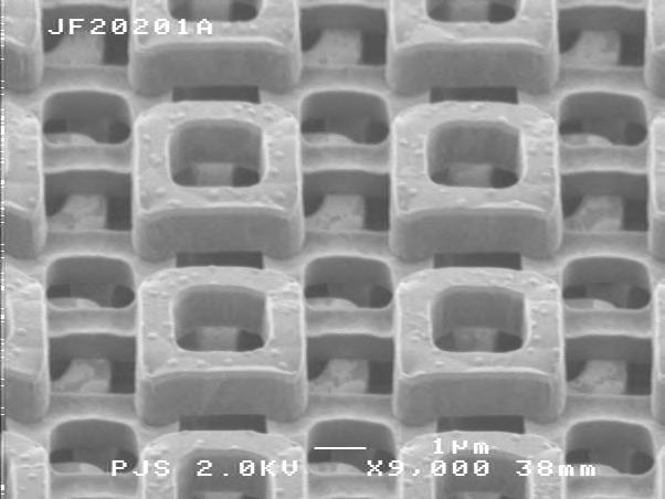

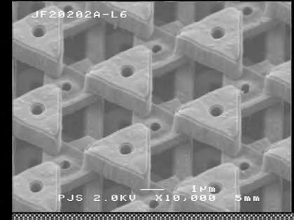
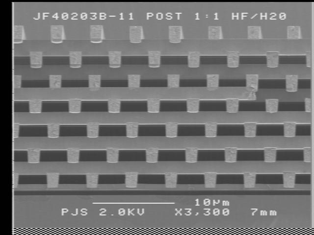
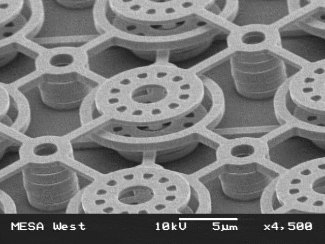

6 Distinguishing Enabler: Tungsten 3-D Fabrication Process The process is low temperature (CMOS compatible), and can be used to fabricate highly complex structures from dielectrics and tungsten 6


7 SNL Ion Trap Chip with 3D Optical Access Linear ion trap chip micro -fabricated with a metal MEMS process at Sandia National Laboratories. Planar metallic trap electrodes (W overcoated with Au) and a hole through the Si substrate define the trapping region and a llow 3D optical access for lasers to ions trapped between RF leads stretched len gthwise over the hole. Control electrodes at the hole edges define seven trapping segme nts. Air bridge metal leads reduce capacitance and RF dissipation to the substra te. 7
8 Photonic crystal research The Why: insurmountable problems in electronic circuits Bandwidth (few GHz) high inductances from small wire features. Thermal issues (fast degradation in performance at elevated temperatures). Slow interchip communication and signal synchronization issues limits high speed interchip communications. An optical solution is needed Photonic crystal offers a new perspective to these problems: Guide and bend light in a unique way. Photonic crystal light source such as selective emitter and thresholdless lasers. Large density of states at the bandedge can be used to control radiative processes of quantum dot systems. Fabrication technologies are compatible to microelectronic tool sets. 8

 Angle (degree) 3) This enables a high level of control over optical")
 2) Sandia is developing novel Photonic Lattice designs.")
9 Si 3-D Photonic Lattice Revolutionizing Photonics Energy (mev) 1) Photonic lattices - the optical analogues of semiconductors CB Edge Κ X' Photonic Band Gap VB Edge Wavelength ( µ m) Angle (degree) 3) This enables a high level of control over optical properties. Transmission Amp. (% layers > 98% attenuation Wavelength µ ( m) 2) Sandia is developing novel Photonic Lattice designs. 4) Si processing enables the development of well defined structures. 9

10 Thermal emission from photonic crystals Planck spectrum Non-equilibrium condition Photonic crystal emission, emissivity close to 1 (equilibrium condition) Unique properties of photonic crystal emission High spectral emissivity in narrow spectral range. Spectral emissivity is fairly independent to temperature. Tunable by crystal design and angle tuning. Emitted power BB cavity Heater Wavelength Photonic crystal Forbidden due to photonic bandgap Heater Physics questions : Emissivity is a thermodynamical quantity describing equilibrium property of electrons, photons and phonons interacting in a common space. In metallic photonic crystal, photons and other entities do not occupy the same space except on the surface. It is interesting to study what are the conditions to drive a photonic crystal system out of equilibrium. Sample clamp Emissivity measurements Temperature of the emitter. Detector gain response. Detector spectral response. 10
.")
11 Spectral intensity response Detector response is nonlinear. Cubic fit the detector response for each wavelength (1490 points). The actual intensity for each wavelength (1490 of them) is determined by solving the cubic equation. 11
 6.")


12 Thermal analysis Silicon thickness=653 um T(hot) 6.8 mm 1.6 mm 1.6 mm Heat loss from the silicon is by radiation with emissivity in accordance to its temperature. Use room temperature thermal conductivity. 12

13 Emissivity measurements of photonic crystal Uncoupled model Without temperature correction 13

14 Harvesting multi-exciton energies with photonic crystal Silicon Photonic crystal Infiltrated with quantum dots Solar source to excite multi-exciton states Multiexcitons in quantum dots Solar cell tuned to single exciton energy Solar cell Multiple-exciton energy conversion Use photonic crystal to enhance emission Photocell 1 S e 0.8eV for PbSe QD 1 S h Single exciton Quadexciton Triexciton Biexciton 14
15 Pump beam Single photon source and photonic crystal Single quantum dot Single photon source Two level atom in photonic crystal Photonic crystal structure Quantum information processing requires non-classical light (single photon source). Coupling parameter g = (Rabi_Frequency).(interaction_time) Critical atom number n 0 = 4/3(radiative_lifetime).(dephasing_time)/(Rabi_Frequency) 2. Critical photon number N 0 = 2(radiative_lifetime).(cavity_lifetime)/(Rabi_Frequency) 2. Requirements g ~ dipole moment >1 n 0 ~ V <<1 N 0 ~ V/Q <<1 hν Emission Not allowed Weak coupling Ω hν+ω Allow modes Bandgap (disallowed modes) Strong coupling Quantum dot acts like an atom. Photonic crystals provide high Q and small mode volume. Ideal system to study radiative control and dephasing processes. 15
16 What about phonon control? 16
17 Motivation: Telecom (the why): Radio/Cellular Operation: Acoustic Bandgap Crystals: Why, What, and How? Rx Tx Half Duplex ASP: Electro-Acoustic Coupling Losses: Rx Tx Full Duplex: Requires high resolution steep filtering Figure of merit Q Q Coupling Loss Signal Power Coupling Loss Coupling Loss Analogue Signal Processing: Cascaded insertion losses imply that once we are in the acoustic domain we would like to remain in it! Why not Digital Signal Processing: Requires high power at high frequencies. Low resolution ADC Acoustic Signal Processing ABG s 17
18 Acoustic Bandgap Crystals: The What What does this have to do with PBG s? Direct analogy between 2D Acoustic (phononic) and photonic crystals. Wealth of Literature on 2D PC that can be used as a first iteration for the design and study of ABG crystal applications. PBG Photons 2nd order coupled vector equations with 2 polarizations Light line constraints and ability to couple to free space modes mandates that full control of waves can only be achieved in 3D devices No inherent structural resonances. Finite size leads only to evanescent mode issues. THZ applications require sub-micron length scales Inherently linear ABG Phonons 2rd order coupled Tensor Equations with 3 polarizations Mechanical wave nature and low coupling to air modes along with the possibility of vacuum packaging allow for full control using only 2D devices Inherent physical size dependent structural resonances. GHZ applications require sub-micron length scales Inherently non-linear 18
19 Acoustic Bandgap Crystals: Contrast to Photonic Bandgap Crystals PBG ABG PBG ABG ABG = Superposition of Bragg and Mie Scattering: A cermet topology (disconnected) of high density inclusions in a low density background matrix. Acoustic impedance mismatch between the inclusions and the matrix. A maximization of the gaps is achieved by requiring the ratio of the longitudinal velocity c l to the shear velocity c s values in both the matrix and inclusion to be as close to the fundamental limit of a hard scatterer 2. Challenges: Finding high Q pair systems. Compatibility with AlN and Si-processing techniques for integration Scaling to um size designs. 19


20 Acoustic Bandgap Crystals: Advantages of ABG Circuitry Added Benefits of the Acoustic Domain: High-Q distributed ABG filters at GHz frequencies at significant improvement over current FBAR technologies resulting in new low power radio architectures. Integration of multiple components on one chip with little or no losses at a size that is times smaller than current optical or micro-strip technology Allows for distributed circuit techniques that are commonly used in microwave circuit design to be applied to lower frequency systems (such as cell phones and WLAN) using acoustic rather than EM waves. Speed of Light = 3x10 8 m/s Speed of Sound in SiO = 2 5.8x10³ m/s Optical Delay Line of 1 µs s = 300 m ABG Delay Line of 1 µs s = 5.8 mm ABG delay line is 52,000 times smaller than an optical one! Miniature Filters Delay Lines Phase Shifters Acoustic Signal Processing Power Combiners/Dividers 20
. AlN Piezoelectric transducers (allows us to leverage FBAR low insertion loss technologies). 1 st generation: MHz devices using a 7 Levels Post- CMOS Compatible process.")
 by Mur s s first")
21 Proposed System: Acoustic Bandgap Crystals: Suspended membrane topology of 2D rod arrays of W (ρ( = 19,300 kg/m3, Z = 89 MΩ) M in SiO 2 (ρ = 2,200 kg/m3, Z = 13 MΩ) M matrix (both are high Q materials). AlN Piezoelectric transducers (allows us to leverage FBAR low insertion loss technologies). 1 st generation: MHz devices using a 7 Levels Post- CMOS Compatible process. Modeling: FDTD algorithm for the temporal integration of the full elastic wave equation that incorporates both Lame coefficients. The Path to GHz ABG s Periodic boundary conditions are used at the edges of the cell along the x and y directions and space is terminated along the z axis (direction of propagation) by Mur s s first order absorbing boundary. The time series results collected at the detection point are converted into the frequency domain using the fast Fourier transform. r=0.3a; a=1um ABG > 4 orders of magnitude rejection 21
, can be attributed to: Use of lossless materials in model.")
22 Excellent Qualitative Agreement. Differences due to: Acoustic Bandgap Crystals: Use of bulk properties in the simulation versus actual measured values of the deposited materials. Theoretical gap appears to be wider, (low frequency end is red-shifted and high frequency end is blue shifted), can be attributed to: Use of lossless materials in model. Infinite size extent in the lateral dimensions. Theory Versus Experiment r a Tungsten Scatterer AlN Coupler 22


23 Acoustic Bandgap Crystals: Line Defects: Theory v.s. Experiment Guide Mode y Z y Z 23


24 Proof of Concept and Lessons Learned Phononic Bandgap Recipe. Possibility of introduction of multiple rejection bands per crystal Because of low coupling to air modes 2D periodicity is sufficient and we do not need to go for the more complicated 3D structures. Bandgap > 4 orders of magnitude rejection 14.4 _m 45 _m Tungsten Scatterer Release Pit AlN Coupler Cross-section of the AlN/W ABG That s s not all! 24
25 Phonon Taming by Elastic Bandgaps Idea: Mold and shape the phonon distribution by artificially changing the density of states. Forbidden States N ph gap Allowed States Path: Create the phonon equivalent of the band theory of solids: Allowed states separated by a phonon gap (forbidden phonon states). Approach: C.B. Superpose Mie resonant scattering by individual scattering centers and Bragg scattering due to their periodic arrangement in a lattice. Requires Mie resonances scattering centers and background matrix to be sufficiently separated by an acoustic impedance mismatch. T gap Non Overlapping V.B. Mie Resonances Matrix of Mismatched Impedance 25
26 Energy Harvesting Scheme: Thermal phonon spectrum Thermal To RF: Energy Harvesting and Passive Tagging Engineer Elastic band gap to posses single/multiple rejection bands whose boundaries lie at the desired harvesting frequency Depleted density of phonon states in the rejection band will force multi- phonon processes to perform up/down frequency conversion allowing phonons to escape in the allowed bands Eph1 + Eph2 Eph3 Couple lattice to a Piezoelectric material to generated EM radio signal. Cascade crystals of different periods and/or design a single crystal with multiple higher order bands (overtones) to generate discrete multiple communication channels. + Phononic Crystal rejection bands Frequency Bar Code! up Conversion Down Conversion + Piezoelectric = Crystal RF Emission Spectrum 26
27 Power Economy: Thermal Energy Harvesting Via Elastic Bandgap Phonon Engineering Room temperature produces 40mW/cm 2 of power RF detection limit is in the microwatts (( Impacts Passive Tagging: Converting exh 27
28 Accelerated Cooling and Modification of the Global Heat Capacity Rapid Accelerated Cooling (ballistic( phonon) ) Scheme: Hot Side Conventional: Cold Side Random Phonon Scattering Overall Drift velocity v d Hot Side EBG Solution : Cold Side Directive Phonon Guides Guide Group velocity v g Concerns: Can we engineer the bands so that: V g > V d? Match guide impedance Modification of the Global Heat Capacity: Forbidden States Dos gap Q c p Bulk N ph gap Allowed States E ph Q c p c p c p Bulk E ph (kt) T T 28


29 Phonon Shielding and Acoustic Focusing and Imaging Phonon Shielding Johnson Noise Reduction: 1D EBG 2D EBG Device Ambient Phonons Device Conventional: White Noise Cap on Sensitivity EBG Solution : 1D Phonon Shield 2D Phonon Mirrors on the interconnects Negative Refraction and Acoustic Focusing: super-lens Conserved Frequency ω Pononic band gap Conserved Wavevector k Negative Sloping Bands Negative Refraction negative group-velocity or negative curvature ( eff. mass ): Negative refraction, Super-Lensing Veselago (1968) object negative refraction mediu m im age 29
30 Elastic Bandgap Phonon Engineering Challenges: Scaling Most relevant applications lie in the GHz-to-THz range these require sub-µm to nm length scales. Unclear how the elastic wave equations scale as we go from the continuum length scales (KHz) to the quantum length scales (THz) Back fill thermalization? Unclear how a modification of the phonon distribution affects the heat capacity. Unclear how a phonon insulation scheme for Johnson noise reduction can be setup in a frame work that prevents re-thermalization of the phonon states. Drift Versus Group Velocities and impedance matching. Unclear whether or not we can create a preferred direction for phonon propagation where the group velocity is higher than the drift velocity and hence allow for accelerated cooling. Efficiency of multiphonon processes for up/down frequency conversion? Problem Statement: Phononic crystals offer a unique vehicle for full phonon control and as such open the door to a vast group of novel applications, however there is a great deal of ambiguity in the efficiency of this control and whether or not recipes borrowed from conventional photonic can be immediately applied or not. 30
Surface plasmon waveguides
 Surface plasmon waveguides Introduction Size Mismatch between Scaled CMOS Electronics and Planar Photonics Photonic integrated system with subwavelength scale components CMOS transistor: Medium-sized molecule
Phononic Crystals: Towards the Full Control of Elastic Waves propagation OUTLINE
 Phononic Crystals: Towards the Full Control of Elastic Waves propagation José Sánchez-Dehesa Wave Phenomena Group, Department of Electronic Engineering, Polytechnic University of Valencia, SPAIN. OUTLINE
Nanomaterials and their Optical Applications
 Nanomaterials and their Optical Applications Winter Semester 2012 Lecture 08 rachel.grange@uni-jena.de http://www.iap.uni-jena.de/multiphoton Outline: Photonic crystals 2 1. Photonic crystals vs electronic
Center for Integrated Nanotechnologies (CINT) Bob Hwang Co-Director, Sandia National Laboratories
 Bob Hwang Co-Director, Sandia National Laboratories") Center for Integrated Nanotechnologies (CINT) Bob Hwang Co-Director, Sandia National Laboratories Department of Energy Nanoscience Centers Molecular Foundry Center for Nanoscale Materials Center for Functional
Center for Integrated Nanotechnologies (CINT) Bob Hwang Co-Director, Sandia National Laboratories Department of Energy Nanoscience Centers Molecular Foundry Center for Nanoscale Materials Center for Functional
Nanophysics: Main trends
 Nano-opto-electronics Nanophysics: Main trends Nanomechanics Main issues Light interaction with small structures Molecules Nanoparticles (semiconductor and metallic) Microparticles Photonic crystals Nanoplasmonics
Photonic Crystal Nanocavities for Efficient Light Confinement and Emission
 Journal of the Korean Physical Society, Vol. 42, No., February 2003, pp. 768 773 Photonic Crystal Nanocavities for Efficient Light Confinement and Emission Axel Scherer, T. Yoshie, M. Lončar, J. Vučković
Supplementary Figure 1: SAW transducer equivalent circuit
 Supplementary Figure : SAW transducer equivalent circuit Supplementary Figure : Radiation conductance and susceptance of.6um IDT, experiment & calculation Supplementary Figure 3: Calculated z-displacement
Terahertz sensing and imaging based on carbon nanotubes:
 Terahertz sensing and imaging based on carbon nanotubes: Frequency-selective detection and near-field imaging Yukio Kawano RIKEN, JST PRESTO ykawano@riken.jp http://www.riken.jp/lab-www/adv_device/kawano/index.html
Dielectric Accelerators at CLARA. G. Burt, Lancaster University On behalf of ASTeC, Lancaster U., Liverpool U., U. Manchester, and Oxford U.
 Dielectric Accelerators at CLARA G. Burt, Lancaster University On behalf of ASTeC, Lancaster U., Liverpool U., U. Manchester, and Oxford U. Dielectric Accelerators Types Photonic structures Dielectric
Enhancing the Rate of Spontaneous Emission in Active Core-Shell Nanowire Resonators
 Chapter 6 Enhancing the Rate of Spontaneous Emission in Active Core-Shell Nanowire Resonators 6.1 Introduction Researchers have devoted considerable effort to enhancing light emission from semiconductors
Arbitrary Patterning Techniques for Anisotropic Surfaces, and Line Waves
 Arbitrary Patterning Techniques for Anisotropic Surfaces, and Line Waves Dan Sievenpiper, Jiyeon Lee, and Dia a Bisharat January 11, 2016 1 Outline Arbitrary Anisotropic Surface Patterning Surface wave
Chapter 3 Properties of Nanostructures
 Chapter 3 Properties of Nanostructures In Chapter 2, the reduction of the extent of a solid in one or more dimensions was shown to lead to a dramatic alteration of the overall behavior of the solids. Generally,
Electromagnetic Metamaterials
 Photonic Bandgap and Electromagnetic Metamaterials Andrew Kirk andrew.kirk@mcgill.ca ca Department of Electrical and Computer Engineering McGill Institute for Advanced Materials A Kirk 11/24/2008 Photonic
A tutorial on meta-materials and THz technology
 p.1/49 A tutorial on meta-materials and THz technology Thomas Feurer thomas.feurer@iap.unibe.ch Institute of Applied Physics Sidlerstr. 5, 3012 Bern Switzerland p.2/49 Outline Meta-materials Super-lenses
PRESENTED BY: PROF. S. Y. MENSAH F.A.A.S; F.G.A.A.S UNIVERSITY OF CAPE COAST, GHANA.
 SOLAR CELL AND ITS APPLICATION PRESENTED BY: PROF. S. Y. MENSAH F.A.A.S; F.G.A.A.S UNIVERSITY OF CAPE COAST, GHANA. OUTLINE OF THE PRESENTATION Objective of the work. A brief introduction to Solar Cell
Practical 1P4 Energy Levels and Band Gaps
 Practical 1P4 Energy Levels and Band Gaps What you should learn from this practical Science This practical illustrates some of the points from the lecture course on Elementary Quantum Mechanics and Bonding
Atomic-Photonic Integration (A-PhI) A-Φ Proposers Day
 A-Φ Proposers Day") Atomic-Photonic Integration (A-PhI) A-Φ Proposers Day Dr. John Burke Microsystems Technology Office (MTO) 1 August 2018 1 What is A-PhI? Atomic physics allows for accurate and sensitive measurements. Supporting
Atomic-Photonic Integration (A-PhI) A-Φ Proposers Day Dr. John Burke Microsystems Technology Office (MTO) 1 August 2018 1 What is A-PhI? Atomic physics allows for accurate and sensitive measurements. Supporting
Nanomaterials and their Optical Applications
 Nanomaterials and their Optical Applications Winter Semester 2013 Lecture 02 rachel.grange@uni-jena.de http://www.iap.uni-jena.de/multiphoton Lecture 2: outline 2 Introduction to Nanophotonics Theoretical
Emission Spectra of the typical DH laser
 Emission Spectra of the typical DH laser Emission spectra of a perfect laser above the threshold, the laser may approach near-perfect monochromatic emission with a spectra width in the order of 1 to 10
Coherent THz Noise Sources. T.M.Loftus Dr R.Donnan Dr T.Kreouzis Dr R.Dubrovka
 Coherent THz Noise Sources T.M.Loftus Dr R.Donnan Dr T.Kreouzis Dr R.Dubrovka 1 Noise Source An unusual source Broadband Incoherent Lambertian emission Why consider it? 2 Power from various devices in
Multi-cycle THz pulse generation in poled lithium niobate crystals
 Laser Focus World April 2005 issue (pp. 67-72). Multi-cycle THz pulse generation in poled lithium niobate crystals Yun-Shik Lee and Theodore B. Norris Yun-Shik Lee is an assistant professor of physics
Supplementary Figure 1 Comparison of single quantum emitters on two type of substrates:
 Supplementary Figure 1 Comparison of single quantum emitters on two type of substrates: a, Photoluminescence (PL) spectrum of localized excitons in a WSe 2 monolayer, exfoliated onto a SiO 2 /Si substrate
Quantum Optics in Wavelength Scale Structures
 Quantum Optics in Wavelength Scale Structures SFB Summer School Blaubeuren July 2012 J. G. Rarity University of Bristol john.rarity@bristol.ac.uk Confining light: periodic dielectric structures Photonic
Acoustic metamaterials in nanoscale
 Acoustic metamaterials in nanoscale Dr. Ari Salmi www.helsinki.fi/yliopisto 12.2.2014 1 Revisit to resonances Matemaattis-luonnontieteellinen tiedekunta / Henkilön nimi / Esityksen nimi www.helsinki.fi/yliopisto
J. Price, 1,2 Y. Q. An, 1 M. C. Downer 1 1 The university of Texas at Austin, Department of Physics, Austin, TX
 Understanding process-dependent oxygen vacancies in thin HfO 2 /SiO 2 stacked-films on Si (100) via competing electron-hole injection dynamic contributions to second harmonic generation. J. Price, 1,2
Introduction to Photonic Crystals
 1 Introduction to Photonic Crystals Summary. Chapter 1 gives a brief introduction into the basics of photonic crystals which are a special class of optical media with periodic modulation of permittivity.
Solar Cell Materials and Device Characterization
 Solar Cell Materials and Device Characterization April 3, 2012 The University of Toledo, Department of Physics and Astronomy SSARE, PVIC Principles and Varieties of Solar Energy (PHYS 4400) and Fundamentals
External (differential) quantum efficiency Number of additional photons emitted / number of additional electrons injected
 quantum efficiency Number of additional photons emitted / number of additional electrons injected") Semiconductor Lasers Comparison with LEDs The light emitted by a laser is generally more directional, more intense and has a narrower frequency distribution than light from an LED. The external efficiency
Semiconductor Lasers Comparison with LEDs The light emitted by a laser is generally more directional, more intense and has a narrower frequency distribution than light from an LED. The external efficiency
Spectroscopy of. Semiconductors. Luminescence OXFORD IVAN PELANT. Academy ofsciences of the Czech Republic, Prague JAN VALENTA
 Luminescence Spectroscopy of Semiconductors IVAN PELANT Institute ofphysics, v.v.i. Academy ofsciences of the Czech Republic, Prague JAN VALENTA Department of Chemical Physics and Optics Charles University,
Nanocomposite photonic crystal devices
 Nanocomposite photonic crystal devices Xiaoyong Hu, Cuicui Lu, Yulan Fu, Yu Zhu, Yingbo Zhang, Hong Yang, Qihuang Gong Department of Physics, Peking University, Beijing, P. R. China Contents Motivation
Photonic Crystals. Introduction
 Photonic Crystals Introduction Definition Photonic crystals are new, artificialy created materials, in which refractive index is periodically modulated in a scale compared to the wavelength of operation.
Spectral Selectivity of Photonic Crystal Infrared Photodetectors
 Spectral Selectivity of Photonic Crystal Infrared Photodetectors Li Chen, Weidong Zhou *, Zexuan Qiang Department of Electrical Engineering University of Texas at Arlington, TX 769-72 Gail J. Brown Air
Plasmonics. The long wavelength of light ( μm) creates a problem for extending optoelectronics into the nanometer regime.
 creates a problem for extending optoelectronics into the nanometer regime.") Plasmonics The long wavelength of light ( μm) creates a problem for extending optoelectronics into the nanometer regime. A possible way out is the conversion of light into plasmons. They have much shorter
Plasmonics The long wavelength of light ( μm) creates a problem for extending optoelectronics into the nanometer regime. A possible way out is the conversion of light into plasmons. They have much shorter
Refraction and Dispersion in Nonlinear Photonic Crystal Superlattices
 Refraction and Dispersion in Nonlinear Photonic Crystal Superlattices LEOS 18 th Annual Meeting Sydney, Australia Monday, 24 October 2005 Curtis W. Neff, Tsuyoshi Yamashita and Christopher J. Summers Presented
Laser Diodes. Revised: 3/14/14 14: , Henry Zmuda Set 6a Laser Diodes 1
 Laser Diodes Revised: 3/14/14 14:03 2014, Henry Zmuda Set 6a Laser Diodes 1 Semiconductor Lasers The simplest laser of all. 2014, Henry Zmuda Set 6a Laser Diodes 2 Semiconductor Lasers 1. Homojunction
Optical Properties of Semiconductors. Prof.P. Ravindran, Department of Physics, Central University of Tamil Nadu, India
 Optical Properties of Semiconductors 1 Prof.P. Ravindran, Department of Physics, Central University of Tamil Nadu, India http://folk.uio.no/ravi/semi2013 Light Matter Interaction Response to external electric
Practical 1P4 Energy Levels and Band Gaps
 Practical 1P4 Energy Levels and Band Gaps What you should learn from this practical Science This practical illustrates some of the points from the lecture course on Elementary Quantum Mechanics and Bonding
Appendix. Photonic crystal lasers: future integrated devices
 91 Appendix Photonic crystal lasers: future integrated devices 5.1 Introduction The technology of photonic crystals has produced a large variety of new devices. However, photonic crystals have not been
Chapter 7. Solar Cell
 Chapter 7 Solar Cell 7.0 Introduction Solar cells are useful for both space and terrestrial application. Solar cells furnish the long duration power supply for satellites. It converts sunlight directly
Chapter Two. Energy Bands and Effective Mass
 Chapter Two Energy Bands and Effective Mass Energy Bands Formation At Low Temperature At Room Temperature Valence Band Insulators Metals Effective Mass Energy-Momentum Diagrams Direct and Indirect Semiconduction
Introduction to semiconductor nanostructures. Peter Kratzer Modern Concepts in Theoretical Physics: Part II Lecture Notes
 Introduction to semiconductor nanostructures Peter Kratzer Modern Concepts in Theoretical Physics: Part II Lecture Notes What is a semiconductor? The Fermi level (chemical potential of the electrons) falls
Three-Dimensional Silicon-Germanium Nanostructures for Light Emitters and On-Chip Optical. Interconnects
 Three-Dimensional Silicon-Germanium Nanostructures for Light Emitters and On-Chip Optical eptember 2011 Interconnects Leonid Tsybeskov Department of Electrical and Computer Engineering New Jersey Institute
The Nature of Accelerating Modes in PBG Fibers
 SLAC-PUB-14029 The Nature of Accelerating Modes in PBG Fibers Robert J. Noble SLAC National Accelerator Laboratory, 2575 Sand Hill Road, Menlo Park, CA 94025 USA Abstract. Transverse magnetic (TM) modes
Optical Investigation of the Localization Effect in the Quantum Well Structures
 Department of Physics Shahrood University of Technology Optical Investigation of the Localization Effect in the Quantum Well Structures Hamid Haratizadeh hamid.haratizadeh@gmail.com IPM, SCHOOL OF PHYSICS,
3.1 Introduction to Semiconductors. Y. Baghzouz ECE Department UNLV
 3.1 Introduction to Semiconductors Y. Baghzouz ECE Department UNLV Introduction In this lecture, we will cover the basic aspects of semiconductor materials, and the physical mechanisms which are at the
Wednesday 3 September Session 3: Metamaterials Theory (16:15 16:45, Huxley LT308)
") Session 3: Metamaterials Theory (16:15 16:45, Huxley LT308) (invited) TBC Session 3: Metamaterials Theory (16:45 17:00, Huxley LT308) Light trapping states in media with longitudinal electric waves D McArthur,
Session 3: Metamaterials Theory (16:15 16:45, Huxley LT308) (invited) TBC Session 3: Metamaterials Theory (16:45 17:00, Huxley LT308) Light trapping states in media with longitudinal electric waves D McArthur,
Ultra-Slow Light Propagation in Room Temperature Solids. Robert W. Boyd
 Ultra-Slow Light Propagation in Room Temperature Solids Robert W. Boyd The Institute of Optics and Department of Physics and Astronomy University of Rochester, Rochester, NY USA http://www.optics.rochester.edu
Mat. Res. Soc. Symp. Proc. Vol Materials Research Society K5.6
 Mat. Res. Soc. Symp. Proc. Vol. 692 2002 Materials Research Society K5.6 Simulations of Realizable Photonic Bandgap Structures with High Refractive Contrast ABSTRACT Bonnie Gersten and Jennifer Synowczynski
Spatio-Temporal Characterization of Bio-acoustic Scatterers in Complex Media
 DISTRIBUTION STATEMENT A. Approved for public release; distribution is unlimited. Spatio-Temporal Characterization of Bio-acoustic Scatterers in Complex Media Karim G. Sabra, School of Mechanical Engineering,
what happens if we make materials smaller?
 what happens if we make materials smaller? IAP VI/10 ummer chool 2007 Couvin Prof. ns outline Introduction making materials smaller? ynthesis how do you make nanomaterials? Properties why would you make
Device 3D. 3D Device Simulator. Nano Scale Devices. Fin FET
 Device 3D 3D Device Simulator Device 3D is a physics based 3D device simulator for any device type and includes material properties for the commonly used semiconductor materials in use today. The physical
Effects from the Thin Metallic Substrate Sandwiched in Planar Multilayer Microstrip Lines
 Progress In Electromagnetics Research Symposium 2006, Cambridge, USA, March 26-29 115 Effects from the Thin Metallic Substrate Sandwiched in Planar Multilayer Microstrip Lines L. Zhang and J. M. Song Iowa
THz experiments at the UCSB FELs and the THz Science and Technology Network.
 THz experiments at the UCSB FELs and the THz Science and Technology Network. Mark Sherwin UCSB Physics Department and Institute for Quantum and Complex Dynamics UCSB Center for Terahertz Science and Technology
transmission reflection absorption
 Optical Cages V. Kumar*, J. P. Walker* and H. Grebel The Electronic Imaging Center and the ECE department at NJIT, Newark, NJ 0702. grebel@njit.edu * Contributed equally Faraday Cage [], a hollow structure
Electronic and Optoelectronic Properties of Semiconductor Structures
 Electronic and Optoelectronic Properties of Semiconductor Structures Jasprit Singh University of Michigan, Ann Arbor CAMBRIDGE UNIVERSITY PRESS CONTENTS PREFACE INTRODUCTION xiii xiv 1.1 SURVEY OF ADVANCES
Sub-wavelength electromagnetic structures
 Sub-wavelength electromagnetic structures Shanhui Fan, Z. Ruan, L. Verselegers, P. Catrysse, Z. Yu, J. Shin, J. T. Shen, G. Veronis Ginzton Laboratory, Stanford University http://www.stanford.edu/group/fan
Terahertz acoustics with multilayers and superlattices Bernard Perrin Institut des NanoSciences de Paris
 Terahertz acoustics with multilayers and superlattices Bernard Perrin Institut des NanoSciences de Paris Daniel Lanzillotti-Kimura CNEA Bariloche & INSP Paris Florencia Pascual-Winter CNEA Bariloche &
The Dielectric Function of a Metal ( Jellium )
") The Dielectric Function of a Metal ( Jellium ) Total reflection Plasma frequency p (10 15 Hz range) Why are Metals Shiny? An electric field cannot exist inside a metal, because metal electrons follow the
The Dielectric Function of a Metal ( Jellium ) Total reflection Plasma frequency p (10 15 Hz range) Why are Metals Shiny? An electric field cannot exist inside a metal, because metal electrons follow the
Optical Properties of Solid from DFT
 Optical Properties of Solid from DFT 1 Prof.P. Ravindran, Department of Physics, Central University of Tamil Nadu, India & Center for Materials Science and Nanotechnology, University of Oslo, Norway http://folk.uio.no/ravi/cmt15
Tailorable stimulated Brillouin scattering in nanoscale silicon waveguides.
 Tailorable stimulated Brillouin scattering in nanoscale silicon waveguides. Heedeuk Shin 1, Wenjun Qiu 2, Robert Jarecki 1, Jonathan A. Cox 1, Roy H. Olsson III 1, Andrew Starbuck 1, Zheng Wang 3, and
Photonic devices for quantum information processing:
 Outline Photonic devices for quantum information processing: coupling to dots, structure design and fabrication Optoelectronics Group, Cavendish Lab Outline Vuckovic s group Noda s group Outline Outline
Review of Optical Properties of Materials
 Review of Optical Properties of Materials Review of optics Absorption in semiconductors: qualitative discussion Derivation of Optical Absorption Coefficient in Direct Semiconductors Photons When dealing
OPTI510R: Photonics. Khanh Kieu College of Optical Sciences, University of Arizona Meinel building R.626
 OPTI510R: Photonics Khanh Kieu College of Optical Sciences, University of Arizona kkieu@optics.arizona.edu Meinel building R.626 Announcements HW#3 is assigned due Feb. 20 st Mid-term exam Feb 27, 2PM
Single Emitter Detection with Fluorescence and Extinction Spectroscopy
 Single Emitter Detection with Fluorescence and Extinction Spectroscopy Michael Krall Elements of Nanophotonics Associated Seminar Recent Progress in Nanooptics & Photonics May 07, 2009 Outline Single molecule
MASSACHUSETTS INSTITUTE OF TECHNOLOGY Physics Department Statistical Physics I Spring Term 2013
 MASSACHUSETTS INSTITUTE OF TECHNOLOGY Physics Department 8.044 Statistical Physics I Spring Term 2013 Problem 1: The Big Bang Problem Set #9 Due in hand-in box by 4;00 PM, Friday, April 19 Early in the
Laser Basics. What happens when light (or photon) interact with a matter? Assume photon energy is compatible with energy transition levels.
 interact with a matter? Assume photon energy is compatible with energy transition levels.") What happens when light (or photon) interact with a matter? Assume photon energy is compatible with energy transition levels. Electron energy levels in an hydrogen atom n=5 n=4 - + n=3 n=2 13.6 = [ev]
What happens when light (or photon) interact with a matter? Assume photon energy is compatible with energy transition levels. Electron energy levels in an hydrogen atom n=5 n=4 - + n=3 n=2 13.6 = [ev]
Quantum Optics in Photonic Crystals. Peter Lodahl Dept. of Communications, Optics & Materials (COM) Technical University of Denmark
 Technical University of Denmark") Quantum Optics in Photonic Crystals Peter Lodahl Dept. of Communications, Optics & Materials (COM) Technical University of Denmark Acknowledgements AMOLF Institute Amsterdam / University of Twente Ivan
Quantum Optics in Photonic Crystals Peter Lodahl Dept. of Communications, Optics & Materials (COM) Technical University of Denmark Acknowledgements AMOLF Institute Amsterdam / University of Twente Ivan
Photonic crystals. Semi-conductor crystals for light. The smallest dielectric lossless structures to control whereto and how fast light flows
 Photonic crystals Semi-conductor crystals for light The smallest dielectric lossless structures to control whereto and how fast light flows Femius Koenderink Center for Nanophotonics AMOLF, Amsterdam f.koenderink@amolf.nl
Acoustic Velocity, Impedance, Reflection, Transmission, Attenuation, and Acoustic Etalons
 Acoustic Velocity, Impedance, Reflection, Transmission, Attenuation, and Acoustic Etalons Acoustic Velocity The equation of motion in a solid is (1) T = ρ 2 u t 2 (1) where T is the stress tensor, ρ is
Nanoacoustics II Lecture #2 More on generation and pick-up of phonons
 Nanoacoustics II Lecture #2 More on generation and pick-up of phonons Dr. Ari Salmi www.helsinki.fi/yliopisto 26.3.2018 1 Last lecture key points Coherent acoustic phonons = sound at nanoscale Incoherent
Quantum Information Processing with Electrons?
 Quantum Information Processing with 10 10 Electrons? René Stock IQIS Seminar, October 2005 People: Barry Sanders Peter Marlin Jeremie Choquette Motivation Quantum information processing realiations Ions
Nanoscale confinement of photon and electron
 Nanoscale confinement of photon and electron Photons can be confined via: Planar waveguides or microcavities (2 d) Optical fibers (1 d) Micro/nano spheres (0 d) Electrons can be confined via: Quantum well
High Power Diode Lasers
 Lecture 10/1 High Power Diode Lasers Low Power Lasers (below tenth of mw) - Laser as a telecom transmitter; - Laser as a spectroscopic sensor; - Laser as a medical diagnostic tool; - Laser as a write-read
Interaction between surface acoustic waves and a transmon qubit
 Interaction between surface acoustic waves and a transmon qubit Ø Introduction Ø Artificial atoms Ø Surface acoustic waves Ø Interaction with a qubit on GaAs Ø Nonlinear phonon reflection Ø Listening to
ESS 5855 Surface Engineering for. MicroElectroMechanicalechanical Systems. Fall 2010
 ESS 5855 Surface Engineering for Microelectromechanical Systems Fall 2010 MicroElectroMechanicalechanical Systems Miniaturized systems with integrated electrical and mechanical components for actuation
University of Louisville - Department of Chemistry, Louisville, KY; 2. University of Louisville Conn Center for renewable energy, Louisville, KY; 3
 Ultrafast transient absorption spectroscopy investigations of charge carrier dynamics of methyl ammonium lead bromide (CH 3 NH 3 PbBr 3 ) perovskite nanostructures Hamzeh Telfah 1 ; Abdelqader Jamhawi
Single Photon detectors
 Single Photon detectors Outline Motivation for single photon detection Semiconductor; general knowledge and important background Photon detectors: internal and external photoeffect Properties of semiconductor
Highly Efficient and Anomalous Charge Transfer in van der Waals Trilayer Semiconductors
 Highly Efficient and Anomalous Charge Transfer in van der Waals Trilayer Semiconductors Frank Ceballos 1, Ming-Gang Ju 2 Samuel D. Lane 1, Xiao Cheng Zeng 2 & Hui Zhao 1 1 Department of Physics and Astronomy,
Chapter 4. Photodetectors
 Chapter 4 Photodetectors Types of photodetectors: Photoconductos Photovoltaic Photodiodes Avalanche photodiodes (APDs) Resonant-cavity photodiodes MSM detectors In telecom we mainly use PINs and APDs.
Course overview. Me: Dr Luke Wilson. The course: Physics and applications of semiconductors. Office: E17 open door policy
 Course overview Me: Dr Luke Wilson Office: E17 open door policy email: luke.wilson@sheffield.ac.uk The course: Physics and applications of semiconductors 10 lectures aim is to allow time for at least one
Chapter 5. Semiconductor Laser
 Chapter 5 Semiconductor Laser 5.0 Introduction Laser is an acronym for light amplification by stimulated emission of radiation. Albert Einstein in 1917 showed that the process of stimulated emission must
Radiation-matter interaction.
 Radiation-matter interaction Radiation-matter interaction Classical dipoles Dipole radiation Power radiated by a classical dipole in an inhomogeneous environment The local density of optical states (LDOS)
Supplementary Materials
 Supplementary Materials Sample characterization The presence of Si-QDs is established by Transmission Electron Microscopy (TEM), by which the average QD diameter of d QD 2.2 ± 0.5 nm has been determined
interband transitions in semiconductors M. Fox, Optical Properties of Solids, Oxford Master Series in Condensed Matter Physics
 interband transitions in semiconductors M. Fox, Optical Properties of Solids, Oxford Master Series in Condensed Matter Physics interband transitions in quantum wells Atomic wavefunction of carriers in
EE C245 ME C218 Introduction to MEMS Design
 EE C245 ME C218 Introduction to MEMS Design Fall 2007 Prof. Clark T.-C. Nguyen Dept. of Electrical Engineering & Computer Sciences University of California at Berkeley Berkeley, CA 94720 Lecture 12: Mechanical
Temperature Dependent Optical Band Gap Measurements of III-V films by Low Temperature Photoluminescence Spectroscopy
 Temperature Dependent Optical Band Gap Measurements of III-V films by Low Temperature Photoluminescence Spectroscopy Linda M. Casson, Francis Ndi and Eric Teboul HORIBA Scientific, 3880 Park Avenue, Edison,
Optical Properties of Lattice Vibrations
 Optical Properties of Lattice Vibrations For a collection of classical charged Simple Harmonic Oscillators, the dielectric function is given by: Where N i is the number of oscillators with frequency ω
Air-holes radius change effects and structure transitions in the linear photonic crystal nanocavities
 American Journal of Optics and Photonics 2013; 1(3): 11-16 Published online June 20, 2013 (http://www.sciencepublishinggroup.com/j/ajop) doi: 10.11648/j.ajop.20130103.11 Air-holes radius change effects
Nanoscale Energy Conversion and Information Processing Devices - NanoNice - Photoacoustic response in mesoscopic systems
 Nanoscale Energy Conversion and Information Processing Devices - NanoNice - Photoacoustic response in mesoscopic systems Photonics group W. Claeys, S. Dilhair, S. Grauby, JM. Rampnoux, L. Patino Lopez,
Semiconductor Optoelectronics Prof. M. R. Shenoy Department of Physics Indian Institute of Technology, Delhi
 Semiconductor Optoelectronics Prof. M. R. Shenoy Department of Physics Indian Institute of Technology, Delhi Lecture - 1 Context and Scope of the Course (Refer Slide Time: 00:44) Welcome to this course
QUESTION BANK IN PHYSICS
 QUESTION BANK IN PHYSICS LASERS. Name some properties, which make laser light different from ordinary light. () {JUN 5. The output power of a given laser is mw and the emitted wavelength is 630nm. Calculate
Nanoscale optical circuits: controlling light using localized surface plasmon resonances
 Nanoscale optical circuits: controlling light using localized surface plasmon resonances T. J. Davis, D. E. Gómez and K. C. Vernon CSIRO Materials Science and Engineering Localized surface plasmon (LSP)
Lasers. Stimulated Emission Lasers: Trapping Photons Terahertz Lasers Course Overview
 Lasers Stimulated Emission Lasers: Trapping Photons Terahertz Lasers Course Overview 1 P-N Junctions and LEDs Terminal Pins Emitted Light Beams Diode Transparent Plastic Case High energy electrons (n-type)
Quality Factor Thickness (nm) Quality Factor Thickness (nm) Quality Factor 10
 Quality Factor Thickness (nm) Quality Factor 10") Oxygen-Terminated Fluorine-Terminated Length = 24 mm Length = 2 mm Length = 1 mm Length = 12 mm Length = 8 mm 8 mm Width, K 12 mm Width, K 1 mm Width, K 8 mm Width, K 12 mm Width, K 1 mm Width, K Supplementary
Oxygen-Terminated Fluorine-Terminated Length = 24 mm Length = 2 mm Length = 1 mm Length = 12 mm Length = 8 mm 8 mm Width, K 12 mm Width, K 1 mm Width, K 8 mm Width, K 12 mm Width, K 1 mm Width, K Supplementary
History of photonic crystals and metamaterials. However, many serious obstacles must be overcome before the impressive possibilities
 TECHNICAL NOTEBOOK I back to basics BACK TO BASICS: History of photonic crystals and metamaterials Costas M. SOUKOULIS 1,2 1 Ames Laboratory and Department of Physics, Iowa State University, Ames, Iowa,
Electroluminescence from Silicon and Germanium Nanostructures
 Electroluminescence from silicon Silicon Getnet M. and Ghoshal S.K 35 ORIGINAL ARTICLE Electroluminescence from Silicon and Germanium Nanostructures Getnet Melese* and Ghoshal S. K.** Abstract Silicon
Confocal Microscopy Imaging of Single Emitter Fluorescence and Hanbury Brown and Twiss Photon Antibunching Setup
 1 Confocal Microscopy Imaging of Single Emitter Fluorescence and Hanbury Brown and Twiss Photon Antibunching Setup Abstract Jacob Begis The purpose of this lab was to prove that a source of light can be
Nanomechanics II. Why vibrating beams become interesting at the nanoscale. Andreas Isacsson Department of Physics Chalmers University of Technology
 Nanomechanics II Why vibrating beams become interesting at the nanoscale Andreas Isacsson Department of Physics Chalmers University of Technology Continuum mechanics Continuum mechanics deals with deformation
Electron Energy, E E = 0. Free electron. 3s Band 2p Band Overlapping energy bands. 3p 3s 2p 2s. 2s Band. Electrons. 1s ATOM SOLID.
 Electron Energy, E Free electron Vacuum level 3p 3s 2p 2s 2s Band 3s Band 2p Band Overlapping energy bands Electrons E = 0 1s ATOM 1s SOLID In a metal the various energy bands overlap to give a single
Microfibres for Quantum Optics. Dr Síle Nic Chormaic Quantum Optics Group
 Microfibres for Quantum Optics Dr Síle Nic Chormaic Quantum Optics Group Motivation Strong need to engineer atoms and photons for the development of new technologies quantum technologies Future advances