Arbitrary Patterning Techniques for Anisotropic Surfaces, and Line Waves
|
|
|
- Branden Rodgers
- 5 years ago
- Views:
Transcription
1 Arbitrary Patterning Techniques for Anisotropic Surfaces, and Line Waves Dan Sievenpiper, Jiyeon Lee, and Dia a Bisharat January 11,
2 Outline Arbitrary Anisotropic Surface Patterning Surface wave propagation and control Radiation and polarization control Scattering control Progress this year: Developed verification method for impedance tensor of complex cell patterns Demonstrated functions that are difficult or impossible with other methods Nearly completed method for generating starting function Line waves New kind of waveguide with field singularity Topological photonic insulator Reconfigurable THz or photonic circuits Progress this year: Conceived of entire concept and determined TPI properties Demonstrated in simulation and verified in experiments Developed concept of reconfigurable THz circuits in graphene 2


3 Example Applications of Anisotropic Impedance Surfaces Guiding and Scattering Anisotropic waveguides can be non-scattering for other directions Boundaries between regions can control wave propagation and scattering 3
 Problem Solution")


4 What Problem Are We Trying to Solve? (Mathematical Approach to RF Snakeskin ) Problem Solution Anisotropic impedance surfaces provide significant advantages to propagation and scattering problems, but they are not easy to make into arbitrary patterns. Develop verifiable approach to generating arbitrary anisotropic surfaces that can perform valuable RF functions 4


5 Point Shifting and Voronoi Cell Generation Method f = 5x 20 Sin[.5 x + y ; 5 10Cos[0.5x + y, 20Cos[0.5x + y Starting function Gradient Point grid (529 points) Voronoi cell generation Unit cell pattern after Voronoi function is applied to the point grid Produces smoothly varying cells with various sizes and orientations Previously demonstrated planar lenses, beam shifting patterns 5


6 Examples of Range of Capabilities Varying Shape Varying Size Varying Direction Extreme and Arbitrary Anisotropy Can make cells that vary in size, shape, and orientation Enables functions that would be difficult to produce by other methods 6

7 How to Characterize the Impedance of Non-Symmetric Anisotropic Cells Z xx Z yx Z xy Z yy How to calculate impedance tensor? The unit cells created by point shifting method are highly asymmetric, and cannot be analyzed by eigenmode simulations Developing a technique to accurately estimate impedance tensor for arbitrary complex cell shapes 7
, (-0.707, -0.")

8 Moment of Inertia Method to Extract Equivalent Rectangular Cell θ Moment of Inertia I (Polygon) = Eigenvalue = 5.33, 0.33 Eigenvectors = (-0.707, 0.707), (-0.707, ) I x = I y = Moment of Inertia (Rectangle) b/2 b/2 b/2 b/2 h/2 h/2 h/2 h/2 y 2 dydx = bh3 12 = 5.33 x 2 dydx = b3 h 12 = 0.33 Rotation Matrix = Cos θ Sin θ θ = Eigenvectors angle Sin θ Cos θ h = 4 (Length) b = 1 (Width) Procedure of calculating an equivalent rectangle of the polygon 8
9 Examples of Unit Cells and Equivalent Rectangles, with Impedance Estimate Polygon cells appear to have same impedance as their moment of inertia extracted equivalent Method is most accurate when gaps are small compared to cell size. 9


10 Applying Impedance Extraction Method to Large Complex Pattern Move the cell to zero point to calculate inertia moment Z frequency Z yy Propagating length Impedance Transverse length Z equivalent rectangle = z xx 0 0 z yy Find an equivalent rectangle and get its impedance from the simulated impedance plot θ Z Polygon = R T Z er R = z xx z xy z yx z yy Applying Jacobian rotation on the Z equivalent rectangle 10


11 Impedance Boundary Simulation with Extracted Impedance Set (1) 5.3 GHz 7.5 GHz PEC patches Impedance Boundary patches 11
 PEC patches")


12 Impedance Boundary Simulation with Extracted Impedance Set (2) PEC patches Impedance Boundary patches Verifying extracted impedance of polygon cells with impedance boundary simulations Field plots are matched with the result of PEC pattern 12


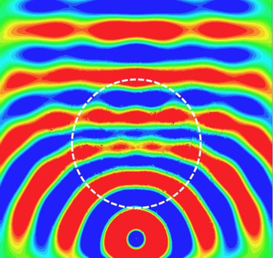
13 90 Degree Curve Pattern Example Near field plot of the surface waves scanned over a mm area The 35mm wide flat wavefronts excited by the feed smoothly move from the bottom edge to the left side edge of the panel 13
14 Inverse Gradient Procedure Tensor matrix Starting function F = F(x, y) F = [ F x,y x, F(x,y) y ] ( F) = x 2 y x x y y x 2 0.5xy y x 0.5y 0.5x + 0.5y F = x 2 dx + x y 0. 25x xy dx dx + x 2 dx x x y -0. 5y dy y x dy + y 2 dy dy 0. 25y xy y x -0. 5x dx + y y dy Take integral of tensor matrix terms and sum up the results (Z xx + Z xy, Z yx + Z yy ) Terms with x and y sometimes have overlapping results, take only one of them 14
15 Inverse Gradient with Starting Function Example Starting function 3y 2 + xy + 50y + x y 2 + xy y x + 6y + 50 y x + 6y 1 Tensor matrix F = x 2 dx + y x xy dy + 3y 2 + xy x y dx dx + y 2 dy dy x 2 dx + y x x y 0 y dx + y 2 x 6y dy dy Constants or 1 st order terms are not restored 15
16 Inverse Gradient with Starting Function Example F = 1 + y x + 6y + 50 F = 3y 2 + xy + 50y + x + 44 F = 3y 2 + xy F = y x + 6y Patterns are same, constants and 1 st order terms in the starting function only affect the location of the pattern i.e. a static offset 16
![Tensor Matrix in Point Shifting Method Starting function F = [ F x,y F(x,y) F = F(x, y), ] ( F) = x y Tensor matrix x 2 y x x y y 2 F = 0.](/docs-images/93/113579312/images/17-1.jpg "5 ( x 2 + y 2 )2 F = [0.707 x 2 + y 2, 0.707 x 2 + y 2 ( F) = 0.5 0.")
17 Tensor Matrix in Point Shifting Method Starting function F = [ F x,y F(x,y) F = F(x, y), ] ( F) = x y Tensor matrix x 2 y x x y y 2 F = 0.5 ( x 2 + y 2 )2 F = [0.707 x 2 + y 2, x 2 + y 2 ( F) = Scale factor ( F) = Z x, y Z o = α tensor matrix Actual impedance of the cell Average impedance 17

18 Tensor function pattern ( F)= 0.06x y 2 F = 0.005x y 4 Y X 18
19 Inverse Gradient Example Planar Lungburg lens function = 1000 e 0.2(x2 +y 2 ) 0.9 Starting Function (previously a guess) Used to Generate Cell Patterns Impedance Tensor Representing Cell Patterns (Verified in Simulations and Experiments) e 0.2(x2 +y 2 ) 0.9 Method Produces Correct Starting Function 19

20 Dan Sievenpiper - UCSD, ,dsievenpiper@eng.ucsd.edu Inverse Gradient of Tensor Matrix Smooth Twist <Tensor matrix plot> Cos x/2 + 1 Cos x + 1 Cos x + 1 Cos y/2 + 1 Cos x y Sin x 2 Cos x + 1 Cos x + 1 Cos y/ Still Working on This Issue x + y y Cos x + 2 Sin y 2 x + y Sin x 2 Sin y 2 1 x 2 y2 + xy Cos x 2 +4 Cos y y Sin x 2 Starting function 20


21 Example from Northrop Grumman Smooth Transition Between Two Impedance Surfaces Received small grant from Northrop Grumman last year to design this pattern
 Inductive Sheet")


22 Line Waves at Impedance Boundaries (A New Kind of Topological Photonic/RF Waveguide with a Field Singularity) Inductive Sheet Capacitive Sheet We can create a line wave at the boundary between two impedance sheets Analogous to surface waves (but one-dimensional instead of two-dimensional) Possibly the smallest waveguide that can be created Contains a field singularity at the center, where nonlinearities can be significant Photonic topological state, so orthogonal modes travel in opposite directions 22


23 Examples of Useful Structures Implemented with Line Waves Route Around Curves Magic T Ring Resonator Coupler Phase Shifter Graphene sheets on layered substrate Can build many of the same structures using line waves as in conventional waveguide, microstrip lines, or in micro-scale photonics applications Can make them electronically reconfigurable on graphene 23


24 Very Low Reflection Even From a Hard Discontinuity, Illustrating Topological State R=377 Field rotates in region above line z=16 z=16 S11 = -10db to -27dB Different propagating directions have opposite polarization Very low scattering from one direction to reverse direction Line waves appear to be EM equivalent to topological insulators Can potentially be used to couple into electronic edge states 24
 Inverse (wire grid) structure forms")

25 Implementation on Capacitive and Inductive FSS Sheets Lattice of discrete metal plates form capacitive side (TE guiding) Inverse (wire grid) structure forms inductive side (TM guiding) Line wave exists at the interface between two frequency selective surfaces Singularity likely limited by the discrete nature of the grids 25
 Inductive Capacitive Measured data shows that line")

26 Broad Bandwidth Operation (Measured Data!) Inductive Capacitive Measured data shows that line waveguide operates over about 2 octaves Only limited by the metal pattern used to implement the surface impedance 26


27 Electronically Reconfigurable Topological THz States in Graphene Graphene has impedance that can be electronically tuned from inductive to capacitive depending on the applied voltage bias Greatest tunability in the THz range, where building complex circuits and devices is also difficult Can create reconfigurable waveguides by defining a pattern of voltages


 to passive")
")

28 Other Related Programs: Nonlinear and Active Metasurfaces (NSF) Add non-foster circuits (negative capacitors and inductors) to passive surface Make phase velocity (and index and impedance) constant over frequency Potential to reach UHF range with practical thickness and cell size 28


29 Other Related Programs: Nonlinear Surfaces for Counter-DEW (ONR) Adding nonlinear circuit elements creates new capabilities in absorbers Demonstrated nonlinear absorption, and waveform dependent absorption Working on nonlinear self-tuning surfaces for frequency agile threats 29


30 Metasurface Enhanced Photoemission (DARPA) Current is controlled by combination of electrical and optical input signals Current Density = 250A/cm 2 Surface Enhanced Raman Scattering (SERS) uses random cavities in rough metal surfaces to create large nonlinear effects by concentrating the optical field Our idea is to engineer the surface to create specific cavity resonances that will enhance the field of an incoming laser beam to perform useful functions 30


31 Theoretical Analysis Suggests Unexpected Levels of Field Enhancement Thermionic Emission Photovoltaic Effect Field Effect Photoemission Combined Field Effect And Photoemission Theory Theory explains photoemission levels only with extreme enhancement: 1800X Possibly due to field extending into the metal, and/or pondermotive forces 31
Wavelength Dependent Microwave Devices Based on Metamaterial Technology. Professor Bal Virdee BSc(Eng) PhD CEng FIET
 PhD CEng FIET") Wavelength Dependent Microwave Devices Based on Metamaterial Technology by Professor Bal Virdee BSc(Eng) PhD CEng FIET EM response of materials are determined by the spatial distribution of its atoms and
Wavelength Dependent Microwave Devices Based on Metamaterial Technology by Professor Bal Virdee BSc(Eng) PhD CEng FIET EM response of materials are determined by the spatial distribution of its atoms and
Applications of Ferroelectrics for Communication Antennas
 Applications of Ferroelectrics for Communication Antennas HRL Research Laboratories Microelectronics Laboratory Jonathan Lynch, jjlynch@hrl.com Joe Colburn, colburn@hrl.com Dave Laney, dclaney@hrl.com
Electron Spin Resonance Study Using Microwave Techniques
 Electron Spin Resonance Study Using Microwave Techniques University of California, Santa Cruz September 12, 2006 Contents 0.1 Introduction......................................... 1 0.2 Kramers-Krönig
TC412 Microwave Communications. Lecture 8 Rectangular waveguides and cavity resonator
 TC412 Microwave Communications Lecture 8 Rectangular waveguides and cavity resonator 1 TM waves in rectangular waveguides Finding E and H components in terms of, WG geometry, and modes. From 2 2 2 xye
New Aspects of Old Equations: Metamaterials and Beyond (Part 2) 신종화 KAIST 물리학과
 신종화 KAIST 물리학과") New Aspects of Old Equations: Metamaterials and Beyond (Part 2) 신종화 KAIST 물리학과 Metamaterial Near field Configuration in Periodic Structures New Material Material and Metamaterial Material Metamaterial
New Aspects of Old Equations: Metamaterials and Beyond (Part 2) 신종화 KAIST 물리학과 Metamaterial Near field Configuration in Periodic Structures New Material Material and Metamaterial Material Metamaterial
Omar M. Ramahi University of Waterloo Waterloo, Ontario, Canada
 Omar M. Ramahi University of Waterloo Waterloo, Ontario, Canada Traditional Material!! Electromagnetic Wave ε, μ r r The only properties an electromagnetic wave sees: 1. Electric permittivity, ε 2. Magnetic
A Dielectric Invisibility Carpet
 A Dielectric Invisibility Carpet Jensen Li Prof. Xiang Zhang s Research Group Nanoscale Science and Engineering Center (NSEC) University of California at Berkeley, USA CLK08-09/22/2008 Presented at Center
Efficiency and Bandwidth Improvement Using Metamaterial of Microstrip Patch Antenna
 Efficiency and Bandwidth Improvement Using Metamaterial of Microstrip Patch Antenna Aakash Mithari 1, Uday Patil 2 1Student Department of Electronics Technology Engg., Shivaji University, Kolhapur, Maharashtra,
Theoretical study of two-element array of equilateral triangular patch microstrip antenna on ferrite substrate
 PRAMANA c Indian Academy of Sciences Vol. 65, No. 3 journal of September 2005 physics pp. 501 512 Theoretical study of two-element array of equilateral triangular patch microstrip antenna on ferrite substrate
DISTRIBUTION A: Distribution approved for public release.
 AFRL-AFOSR-VA-TR-2016-0129 ANISOTROPIC GRID GENERATION Deliverables Daniel Sievenpiper UNIVERSITY OF CALIFORNIA SAN DIEGO 03/24/2016 Final Report Air Force Research Laboratory AF Office Of Scientific Research
4. Integrated Photonics. (or optoelectronics on a flatland)
") 4. Integrated Photonics (or optoelectronics on a flatland) 1 x Benefits of integration in Electronics: Are we experiencing a similar transformation in Photonics? Mach-Zehnder modulator made from Indium
4. Integrated Photonics (or optoelectronics on a flatland) 1 x Benefits of integration in Electronics: Are we experiencing a similar transformation in Photonics? Mach-Zehnder modulator made from Indium
5 RCS Management of Edge Diffracted Waves
 5 RCS Management of Edge Diffracted Waves 5.1 Introduction Radar absorbing materials (RAM s) applied as a coating on the surface of an object, partially transform the energy of an incident radar beam into
Electrodynamics Qualifier Examination
 Electrodynamics Qualifier Examination January 10, 2007 1. This problem deals with magnetostatics, described by a time-independent magnetic field, produced by a current density which is divergenceless,
OPTI510R: Photonics. Khanh Kieu College of Optical Sciences, University of Arizona Meinel building R.626
 OPTI510R: Photonics Khanh Kieu College of Optical Sciences, University of Arizona kkieu@optics.arizona.edu Meinel building R.626 Announcements HW#3 is assigned due Feb. 20 st Mid-term exam Feb 27, 2PM
International Distinguished Lecturer Program
 U 005-006 International Distinguished Lecturer Program Ken-ya Hashimoto Chiba University Sponsored by The Institute of Electrical and Electronics Engineers (IEEE) Ultrasonics, Ferroelectrics and Frequency
Electromagnetics in COMSOL Multiphysics is extended by add-on Modules
 AC/DC Module Electromagnetics in COMSOL Multiphysics is extended by add-on Modules 1) Start Here 2) Add Modules based upon your needs 3) Additional Modules extend the physics you can address 4) Interface
Computational Electromagnetics: from Metamaterials to Particle Accelerators
 Computational Electromagnetics: from Metamaterials to Particle Accelerators Arya Fallahi Ultrafast optics and X-ray Division 1. July 213 2/44 Outline Ø Frequency Selective Surfaces (FSS) Analysis techniques:
Diode Lasers and Photonic Integrated Circuits
 Diode Lasers and Photonic Integrated Circuits L. A. COLDREN S. W. CORZINE University of California Santa Barbara, California A WILEY-INTERSCIENCE PUBLICATION JOHN WILEY & SONS, INC. NEW YORK / CHICHESTER
Gradient-index metamaterials and spoof surface plasmonic waveguide
 Gradient-index metamaterials and spoof surface plasmonic waveguide Hui Feng Ma State Key Laboratory of Millimeter Waves Southeast University, Nanjing 210096, China City University of Hong Kong, 11 October
Angular-Stability Low-Profile Miniaturized Frequency Selective Surface Based on Complementary Structure
 Progress In Electromagnetics Research M, Vol. 57, 119 128, 2017 Angular-Stability Low-Profile Miniaturized Frequency Selective Surface Based on Complementary Structure Wenxing Li and Yuanyuan Li * Abstract
Ansoft HFSS 3D Boundary Manager Sources
 Lumped Gap Defining s Voltage and Current When you select Source, you may choose from the following source types: Incident wave Voltage drop Current Magnetic bias These sources are available only for driven
EECS 117 Lecture 3: Transmission Line Junctions / Time Harmonic Excitation
 EECS 117 Lecture 3: Transmission Line Junctions / Time Harmonic Excitation Prof. Niknejad University of California, Berkeley University of California, Berkeley EECS 117 Lecture 3 p. 1/23 Transmission Line
Analysis of Frequency Behavior of Microstrip Lines on Anisotropic Substrates with Slots in Ground Plane
 18 Analysis of Frequency Behavior of Microstrip Lines on Anisotropic Substrates with Slots in Ground Plane Sachin Singh and Banmali S. Rawat* Department of Electrical Engineering University of Nevada,
A tutorial on meta-materials and THz technology
 p.1/49 A tutorial on meta-materials and THz technology Thomas Feurer thomas.feurer@iap.unibe.ch Institute of Applied Physics Sidlerstr. 5, 3012 Bern Switzerland p.2/49 Outline Meta-materials Super-lenses
Chapter-4 Stimulated emission devices LASERS
 Semiconductor Laser Diodes Chapter-4 Stimulated emission devices LASERS The Road Ahead Lasers Basic Principles Applications Gas Lasers Semiconductor Lasers Semiconductor Lasers in Optical Networks Improvement
Lecture 5: Photoinjector Technology. J. Rosenzweig UCLA Dept. of Physics & Astronomy USPAS, 7/1/04
 Lecture 5: Photoinjector Technology J. Rosenzweig UCLA Dept. of Physics & Astronomy USPAS, 7/1/04 Technologies Magnetostatic devices Computational modeling Map generation RF cavities 2 cell devices Multicell
Coplanar Microwave Integrated Circuits
 Ingo Wolff Coplanar Microwave Integrated Circuits Verlagsbuchhandlung Dr. Wolff GmbH Content Chapter I. 1.1 Chapter II. II. 1 n.1.1 n.1.2 n.1.3 n.1.3.1 n.1.3.2 n.2 n.2.1 n.2.2 n.2.3 n.2.4 n.2.5 n.2.6 n.2.7
(b) Spontaneous emission. Absorption, spontaneous (random photon) emission and stimulated emission.
 Spontaneous emission. Absorption, spontaneous (random photon) emission and stimulated emission.") Lecture 10 Stimulated Emission Devices Lasers Stimulated emission and light amplification Einstein coefficients Optical fiber amplifiers Gas laser and He-Ne Laser The output spectrum of a gas laser Laser
Lecture 10 Stimulated Emission Devices Lasers Stimulated emission and light amplification Einstein coefficients Optical fiber amplifiers Gas laser and He-Ne Laser The output spectrum of a gas laser Laser
Analyzing of Coupling Region for CRLH/RH TL Coupler with Lumped-elements
 PIERS ONLINE, VOL. 3, NO. 5, 27 564 Analyzing of Coupling Region for CRLH/RH TL Coupler with Lumped-elements Y. Wang 2, Y. Zhang, 2, and F. Liu 2 Pohl Institute of Solid State Physics, Tongji University,
Characterising Properties and Loss in High Powered Metamaterials
 Characterising Properties and Loss in High Powered Metamaterials Aimée Hopper PhD Student Supervisor: R. Seviour International Institute for Accelerator Applications University of Huddersfield (UK) Email:
T he reflection phase control for electromagnetic (EM) wave impinging on a surface is important in both
 wave impinging on a surface is important in both") OPEN SUBJECT AREAS: ELECTRICAL AND ELECTRONIC ENGINEERING MATERIALS FOR DEVICES Active impedance metasurface with full 360u reflection phase tuning Bo O. Zhu, Junming Zhao & Yijun Feng School of Electronic
OPEN SUBJECT AREAS: ELECTRICAL AND ELECTRONIC ENGINEERING MATERIALS FOR DEVICES Active impedance metasurface with full 360u reflection phase tuning Bo O. Zhu, Junming Zhao & Yijun Feng School of Electronic
Arbitrary and reconfigurable optics - new opportunities for integrated photonics
 Arbitrary and reconfigurable optics - new opportunities for integrated photonics David Miller, Stanford University For a copy of these slides, please e-mail dabm@ee.stanford.edu How to design any linear
Left-handed materials: Transfer matrix method studies
 Left-handed materials: Transfer matrix method studies Peter Markos and C. M. Soukoulis Outline of Talk What are Metamaterials? An Example: Left-handed Materials Results of the transfer matrix method Negative
Stimulated Emission Devices: LASERS
 Stimulated Emission Devices: LASERS 1. Stimulated Emission and Photon Amplification E 2 E 2 E 2 hυ hυ hυ In hυ Out hυ E 1 E 1 E 1 (a) Absorption (b) Spontaneous emission (c) Stimulated emission The Principle
Engineering Electromagnetics
 Nathan Ida Engineering Electromagnetics With 821 Illustrations Springer Contents Preface vu Vector Algebra 1 1.1 Introduction 1 1.2 Scalars and Vectors 2 1.3 Products of Vectors 13 1.4 Definition of Fields
Cloaking The Road to Realization
 Cloaking The Road to Realization by Reuven Shavit Electrical and Computer Engineering Department Ben-Gurion University of the Negev 1 Outline Introduction Transformation Optics Laplace s Equation- Transformation
Solutions to Problems in Chapter 6
 Appendix F Solutions to Problems in Chapter 6 F.1 Problem 6.1 Short-circuited transmission lines Section 6.2.1 (book page 193) describes the method to determine the overall length of the transmission line
A Novel Tunable Dual-Band Bandstop Filter (DBBSF) Using BST Capacitors and Tuning Diode
 Using BST Capacitors and Tuning Diode") Progress In Electromagnetics Research C, Vol. 67, 59 69, 2016 A Novel Tunable Dual-Band Bandstop Filter (DBBSF) Using BST Capacitors and Tuning Diode Hassan Aldeeb and Thottam S. Kalkur * Abstract A novel
Progress In Electromagnetics Research C, Vol. 67, 59 69, 2016 A Novel Tunable Dual-Band Bandstop Filter (DBBSF) Using BST Capacitors and Tuning Diode Hassan Aldeeb and Thottam S. Kalkur * Abstract A novel
444 Index Boundary condition at transmission line short circuit, 234 for normal component of B, 170, 180 for normal component of D, 169, 180 for tange
 Index A. see Magnetic vector potential. Acceptor, 193 Addition of complex numbers, 19 of vectors, 3, 4 Admittance characteristic, 251 input, 211 line, 251 Ampere, definition of, 427 Ampere s circuital
The Finite-Difference Time-Domain Method for Electromagnetics with MATLAB Simulations
 The Finite-Difference Time-Domain Method for Electromagnetics with MATLAB Simulations Atef Z. Elsherbeni and Veysel Demir SciTech Publishing, Inc Raleigh, NC scitechpublishing.com Contents Preface Author
Laser Optics-II. ME 677: Laser Material Processing Instructor: Ramesh Singh 1
 Laser Optics-II 1 Outline Absorption Modes Irradiance Reflectivity/Absorption Absorption coefficient will vary with the same effects as the reflectivity For opaque materials: reflectivity = 1 - absorptivity
From the Wideröe gap to the linac cell
 Module 3 Coupled resonator chains Stability and stabilization Acceleration in periodic structures Special accelerating structures Superconducting linac structures From the Wideröe gap to the linac cell
School of Electrical and Computer Engineering, Cornell University. ECE 5330: Semiconductor Optoelectronics. Fall 2014
 School of Electrical and Computer Engineering, Cornell University ECE 5330: Semiconductor Optoelectronics Fall 014 Homework 7 Due on Nov. 06, 014 Suggested Readings: i) Study lecture notes. ii) Study Coldren
ELECTROMAGNETIC FIELDS AND WAVES
 ELECTROMAGNETIC FIELDS AND WAVES MAGDY F. ISKANDER Professor of Electrical Engineering University of Utah Englewood Cliffs, New Jersey 07632 CONTENTS PREFACE VECTOR ANALYSIS AND MAXWELL'S EQUATIONS IN
Graphene nanophotonics methods and devices: what can we learn from the microwave field?
 Graphene nanophotonics methods and devices: what can we learn from the microwave field? J. Perruisseau Carrier J. S. Gomez Diaz, M. Tamagnone, E. Carrasco, C. Moldovan, M. Esquius, P. Sharma, J. R. Mosig,
Effects from the Thin Metallic Substrate Sandwiched in Planar Multilayer Microstrip Lines
 Progress In Electromagnetics Research Symposium 2006, Cambridge, USA, March 26-29 115 Effects from the Thin Metallic Substrate Sandwiched in Planar Multilayer Microstrip Lines L. Zhang and J. M. Song Iowa
CST EM : Examples. Chang-Kyun PARK (Ph. D. St.) Thin Films & Devices (TFD) Lab.
 Thin Films & Devices (TFD) Lab.") CST Advanced Training 2004 @ Daedeok Convention Town (2004.03.24) CST EM : Examples TM EM Studio TM Chang-Kyun PARK (Ph. D. St.) E-mail: ckpark@ihanyang.ac.kr Thin Films & Devices (TFD) Lab. Dept. of Electrical
CST Advanced Training 2004 @ Daedeok Convention Town (2004.03.24) CST EM : Examples TM EM Studio TM Chang-Kyun PARK (Ph. D. St.) E-mail: ckpark@ihanyang.ac.kr Thin Films & Devices (TFD) Lab. Dept. of Electrical
Alternative approaches to electromagnetic cloaking and invisibility
 Helsinki University of Technology SMARAD Centre of Excellence Radio Laboratory Alternative approaches to electromagnetic cloaking and invisibility Sergei Tretyakov and colleagues December 2007 What is
Optics, Optoelectronics and Photonics
 Optics, Optoelectronics and Photonics Engineering Principles and Applications Alan Billings Emeritus Professor, University of Western Australia New York London Toronto Sydney Tokyo Singapore v Contents
The Pennsylvania State University The Graduate School UNIAXIAL METAMATERIALS FOR MICROWAVE FAR-FIELD COLLIMATING LENSES
 The Pennsylvania State University The Graduate School UNIAXIAL METAMATERIALS FOR MICROWAVE FAR-FIELD COLLIMATING LENSES A Thesis in Electrical Engineering by Jeremiah Paul Turpin c 211 Jeremiah Paul Turpin
J.-C. Zhang, Y.-Z. Yin, and J.-P. Ma National Laboratory of Antennas and Microwave Technology Xidian University Xi an, Shaanxi , P. R.
 Progress In Electromagnetics Research Letters, Vol. 6, 55 60, 2009 MULTIFUNCTIONAL MEANDER LINE POLARIZER J.-C. Zhang, Y.-Z. Yin, and J.-P. Ma National Laboratory of Antennas and Microwave Technology Xidian
ARTIFICIAL DIELECTRIC SUBSTRATE FOR MICROWAVE APPLICATIONS
 ARTIFICIAL DIELECTRIC SUBSTRATE FOR MICROWAVE APPLICATIONS DOC. ING. JAN MACHÁČ, DRSC. PROF. ING. JÁN ZEHENTNER, DRSC. Abstract: This paper presents a new version of an artificial dielectric substrate.
Light Manipulation by Metamaterials
 Light Manipulation by Metamaterials W. J. Sun, S. Y. Xiao, Q. He*, L. Zhou Physics Department, Fudan University, Shanghai 200433, China *Speaker: qionghe@fudan.edu.cn 2011/2/19 Outline Background of metamaterials
LASER. Light Amplification by Stimulated Emission of Radiation
 LASER Light Amplification by Stimulated Emission of Radiation Energy Level, Definitions The valence band is the highest filled band The conduction band is the next higher empty band The energy gap has
Electromagnetic Waves
 Electromagnetic Waves Our discussion on dynamic electromagnetic field is incomplete. I H E An AC current induces a magnetic field, which is also AC and thus induces an AC electric field. H dl Edl J ds
Sub-wavelength electromagnetic structures
 Sub-wavelength electromagnetic structures Shanhui Fan, Z. Ruan, L. Verselegers, P. Catrysse, Z. Yu, J. Shin, J. T. Shen, G. Veronis Ginzton Laboratory, Stanford University http://www.stanford.edu/group/fan
Wednesday 3 September Session 3: Metamaterials Theory (16:15 16:45, Huxley LT308)
") Session 3: Metamaterials Theory (16:15 16:45, Huxley LT308) (invited) TBC Session 3: Metamaterials Theory (16:45 17:00, Huxley LT308) Light trapping states in media with longitudinal electric waves D McArthur,
Session 3: Metamaterials Theory (16:15 16:45, Huxley LT308) (invited) TBC Session 3: Metamaterials Theory (16:45 17:00, Huxley LT308) Light trapping states in media with longitudinal electric waves D McArthur,
ECE 6340 Fall Homework 2. Please do the following problems (you may do the others for practice if you wish): Probs. 1, 2, 3, 4, 5, 6, 7, 10, 12
: Probs. 1, 2, 3, 4, 5, 6, 7, 10, 12") ECE 634 Fall 16 Homework Please do the following problems (you may do the others for practice if you wish: Probs. 1,, 3, 4, 5, 6, 7, 1, 1 1 Consider two parallel infinite wires in free space each carrying
ECE 634 Fall 16 Homework Please do the following problems (you may do the others for practice if you wish: Probs. 1,, 3, 4, 5, 6, 7, 1, 1 1 Consider two parallel infinite wires in free space each carrying
Supplementary Figure 1. Selected area electron diffraction (SAED) of bilayer graphene and tblg. (a) AB
 of bilayer graphene and tblg. (a) AB") Supplementary Figure 1. Selected area electron diffraction (SAED) of bilayer graphene and tblg. (a) AB stacked bilayer graphene (b), (c), (d), (e), and (f) are twisted bilayer graphene with twist angle
Supplementary Figure 1. Selected area electron diffraction (SAED) of bilayer graphene and tblg. (a) AB stacked bilayer graphene (b), (c), (d), (e), and (f) are twisted bilayer graphene with twist angle
Microstrip Coupler with Complementary Split-Ring Resonator (CSRR)
") Microstrip Coupler with Complementary Split-Ring Resonator (CSRR) E-242 Course Project Report Submitted by, EMIL MATHEW JOSEPH 4810-411-091-07049 Guided by, Prof. K J VINOY Department of Electrical and
Microstrip Coupler with Complementary Split-Ring Resonator (CSRR) E-242 Course Project Report Submitted by, EMIL MATHEW JOSEPH 4810-411-091-07049 Guided by, Prof. K J VINOY Department of Electrical and
Outline of College Physics OpenStax Book
 Outline of College Physics OpenStax Book Taken from the online version of the book Dec. 27, 2017 18. Electric Charge and Electric Field 18.1. Static Electricity and Charge: Conservation of Charge Define
Homework 1. Property LASER Incandescent Bulb
 Homework 1 Solution: a) LASER light is spectrally pure, single wavelength, and they are coherent, i.e. all the photons are in phase. As a result, the beam of a laser light tends to stay as beam, and not
Defense Technical Information Center Compilation Part Notice
 UNCLASSIFIED Defense Technical Information Center Compilation Part Notice ADP012763 TITLE: Absorption Coefficient of InGaAs V-shaped Quantum Wires Integrated in Optical Waveguides by MBE Growth DISTRIBUTION:
Chap. 1 Fundamental Concepts
 NE 2 Chap. 1 Fundamental Concepts Important Laws in Electromagnetics Coulomb s Law (1785) Gauss s Law (1839) Ampere s Law (1827) Ohm s Law (1827) Kirchhoff s Law (1845) Biot-Savart Law (1820) Faradays
Research Article Trapped-Mode Resonance Regime of Thin Microwave Electromagnetic Arrays with Two Concentric Rings in Unit Cell
 Microwave Science and Technology Volume 2, Article ID 3688, 6 pages doi:.55/2/3688 Research Article Trapped-Mode Resonance Regime of Thin Microwave Electromagnetic Arrays with Two Concentric Rings in Unit
Supplementary Figure 1: SAW transducer equivalent circuit
 Supplementary Figure : SAW transducer equivalent circuit Supplementary Figure : Radiation conductance and susceptance of.6um IDT, experiment & calculation Supplementary Figure 3: Calculated z-displacement
PHYSICS 2B FINAL EXAM ANSWERS WINTER QUARTER 2010 PROF. HIRSCH MARCH 18, 2010 Problems 1, 2 P 1 P 2
 Problems 1, 2 P 1 P 1 P 2 The figure shows a non-conducting spherical shell of inner radius and outer radius 2 (i.e. radial thickness ) with charge uniformly distributed throughout its volume. Prob 1:
Reversed Cherenkov Radiation in Left Handed Meta material Lecture, Nov 21, 2012 Prof. Min Chen
 Reversed Cherenkov Radiation in Left Handed Meta material 8.07 Lecture, Nov 21, 2012 Prof. Min Chen 1 8.07 is not just an abstract theory; it is a tool which can be applied to change the world around you.
Quantum computation and quantum information
 Quantum computation and quantum information Chapter 7 - Physical Realizations - Part 2 First: sign up for the lab! do hand-ins and project! Ch. 7 Physical Realizations Deviate from the book 2 lectures,
Canalization of Sub-wavelength Images by Electromagnetic Crystals
 Progress In Electromagnetics Research Symposium 2005, Hangzhou, China, August 22-26 37 Canalization of Sub-wavelength Images by Electromagnetic Crystals P. A. Belov 1 and C. R. Simovski 2 1 Queen Mary
PRE-BOARD EXAMINATION STD : XII MARKS : 150
 PRE-BOARD EXAMINATION STD : XII MARKS : 150 SUB : PHYSICS TIME : 3.00 Hrs I.Choose the correct answer: 30x1=30 1.Which of the following quantities not a scalar? a)electric flux b) electric potential c)
OPTI510R: Photonics. Khanh Kieu College of Optical Sciences, University of Arizona Meinel building R.626
 OPTI510R: Photonics Khanh Kieu College of Optical Sciences, University of Arizona kkieu@optics.arizona.edu Meinel building R.626 Announcements Mid-term exam on Monday, March 6 th Review Properties of light
UNIT I ELECTROSTATIC FIELDS
 UNIT I ELECTROSTATIC FIELDS 1) Define electric potential and potential difference. 2) Name few applications of gauss law in electrostatics. 3) State point form of Ohm s Law. 4) State Divergence Theorem.
1 The formation and analysis of optical waveguides
 1 The formation and analysis of optical waveguides 1.1 Introduction to optical waveguides Optical waveguides are made from material structures that have a core region which has a higher index of refraction
Class XII Physics (Theory)
") DATE : 0/03/209 SET-3 Code No. //3 Regd. Office : Aakash Tower, 8, Pusa Road, New Delhi-000. Ph.: 0-4762346 Class XII Physics (Theory) Time : 3 Hrs. Max. Marks : 70 (CBSE 209) GENERAL INSTRUCTIONS :. All
DATE : 0/03/209 SET-3 Code No. //3 Regd. Office : Aakash Tower, 8, Pusa Road, New Delhi-000. Ph.: 0-4762346 Class XII Physics (Theory) Time : 3 Hrs. Max. Marks : 70 (CBSE 209) GENERAL INSTRUCTIONS :. All
OPTI510R: Photonics. Khanh Kieu College of Optical Sciences, University of Arizona Meinel building R.626
 OPTI510R: Photonics Khanh Kieu College of Optical Sciences, University of Arizona kkieu@optics.arizona.edu Meinel building R.626 Announcements Mid-term exam will be on Feb 27 th, 2PM, room 307 (open books/notes)
Q1. A wave travelling along a string is described by
 Coordinator: Saleem Rao Wednesday, May 24, 2017 Page: 1 Q1. A wave travelling along a string is described by y( x, t) = 0.00327 sin(72.1x 2.72t) In which all numerical constants are in SI units. Find the
OPTI510R: Photonics. Khanh Kieu College of Optical Sciences, University of Arizona Meinel building R.626
 OPTI510R: Photonics Khanh Kieu College of Optical Sciences, University of Arizona kkieu@optics.arizona.edu Meinel building R.626 Announcements No class Monday, Feb 26 Mid-term exam will be on Feb 28 th
ARTIFICIAL TRANSMISSION LINE WITH LEFT/RIGHT-HANDED BEHAVIOR BASED ON WIRE BONDED INTERDIGITAL CAPACITORS
 Progress In Electromagnetics Research B, Vol. 11, 245 264, 29 ARTIFICIAL TRANSMISSION LINE WITH LEFT/RIGHT-HANDED BEHAVIOR BASED ON WIRE BONDED INTERDIGITAL CAPACITORS J. J. Sánchez-Martínez, E. Márquez-Segura,
Surface Plasmon Amplification by Stimulated Emission of Radiation. By: Jonathan Massey-Allard Graham Zell Justin Lau
 Surface Plasmon Amplification by Stimulated Emission of Radiation By: Jonathan Massey-Allard Graham Zell Justin Lau Surface Plasmons (SPs) Quanta of electron oscillations in a plasma. o Electron gas in
NAME: MA Sample Final Exam. Record all your answers on the answer sheet provided. The answer sheet is the only thing that will be graded.
 NAME: MA 300 Sample Final Exam PUID: INSTRUCTIONS There are 5 problems on 4 pages. Record all your answers on the answer sheet provided. The answer sheet is the only thing that will be graded. No books
Road Map. Potential Applications of Antennas with Metamaterial Loading
 Road Map Potential Applications of Antennas with Metamaterial Loading Filiberto Bilotti Department of Applied Electronics University of Roma Tre Rome, Italy The history of metamaterials Metamaterial terminology
REVISED HIGHER PHYSICS REVISION BOOKLET ELECTRONS AND ENERGY
 REVSED HGHER PHYSCS REVSON BOOKLET ELECTRONS AND ENERGY Kinross High School Monitoring and measuring a.c. Alternating current: Mains supply a.c.; batteries/cells supply d.c. Electrons moving back and forth,
1. Consider the biconvex thick lens shown in the figure below, made from transparent material with index n and thickness L.
 Optical Science and Engineering 2013 Advanced Optics Exam Answer all questions. Begin each question on a new blank page. Put your banner ID at the top of each page. Please staple all pages for each individual
Microwave Engineering 3e Author - D. Pozar
 Microwave Engineering 3e Author - D. Pozar Sections 3.6 3.8 Presented by Alex Higgins 1 Outline Section 3.6 Surface Waves on a Grounded Dielectric Slab Section 3.7 Stripline Section 3.8 Microstrip An Investigation
Graduate Diploma in Engineering Circuits and waves
 9210-112 Graduate Diploma in Engineering Circuits and waves You should have the following for this examination one answer book non-programmable calculator pen, pencil, ruler No additional data is attached
Physics 610. Adv Particle Physics. April 7, 2014
 Physics 610 Adv Particle Physics April 7, 2014 Accelerators History Two Principles Electrostatic Cockcroft-Walton Van de Graaff and tandem Van de Graaff Transformers Cyclotron Betatron Linear Induction
SUPPLEMENTARY INFORMATION
 doi:10.1038/nature09776 Supplementary Information for Unnaturally high refractive index terahertz metamaterial Muhan Choi, Seung Hoon Lee, Yushin Kim, Seung Beom Kang, Jonghwa Shin, Min Hwan Kwak, Kwang-Young
Partial discharge (PD) is well established as a diagnostic
 is well established as a diagnostic") F E A T U R E A R T I C L E Application of Maxwell Solvers to PD Propagation Part I: Concepts and Codes Key Words: Partial discharge propagation, electromagnetic field analysis, Maxwell solvers, boundary
F E A T U R E A R T I C L E Application of Maxwell Solvers to PD Propagation Part I: Concepts and Codes Key Words: Partial discharge propagation, electromagnetic field analysis, Maxwell solvers, boundary
Anisotropic Design Considerations for 28 Gbps Via to Stripline Transitions
 DesignCon 2015 Anisotropic Design Considerations for 28 Gbps Via to Stripline Transitions Scott McMorrow, Teraspeed Consulting A Division of Samtec Ed Sayre, Teraspeed Consulting A Division of Samtec Chudy
Electromagnetic Theory for Microwaves and Optoelectronics
 Keqian Zhang Dejie Li Electromagnetic Theory for Microwaves and Optoelectronics Second Edition With 280 Figures and 13 Tables 4u Springer Basic Electromagnetic Theory 1 1.1 Maxwell's Equations 1 1.1.1
Beam propagation method for waveguide device simulation
 1/29 Beam propagation method for waveguide device simulation Chrisada Sookdhis Photonics Research Centre, Nanyang Technological University This is for III-V Group Internal Tutorial Overview EM theory,
requency generation spectroscopy Rahul N
 requency generation spectroscopy Rahul N 2-11-2013 Sum frequency generation spectroscopy Sum frequency generation spectroscopy (SFG) is a technique used to analyze surfaces and interfaces. SFG was first
Nanoscale optical circuits: controlling light using localized surface plasmon resonances
 Nanoscale optical circuits: controlling light using localized surface plasmon resonances T. J. Davis, D. E. Gómez and K. C. Vernon CSIRO Materials Science and Engineering Localized surface plasmon (LSP)
A system of two lenses is achromatic when the separation between them is
 L e c t u r e 1 5 1 Eyepieces Single eye lens in a telescope / microscope produces spherical and chromatic aberrations. The field of view is also narrow. The eye lens is replaced by a system of lenses
CHAPTER 9 ELECTROMAGNETIC WAVES
 CHAPTER 9 ELECTROMAGNETIC WAVES Outlines 1. Waves in one dimension 2. Electromagnetic Waves in Vacuum 3. Electromagnetic waves in Matter 4. Absorption and Dispersion 5. Guided Waves 2 Skip 9.1.1 and 9.1.2
Definition of differential equations and their classification. Methods of solution of first-order differential equations
 Introduction to differential equations: overview Definition of differential equations and their classification Solutions of differential equations Initial value problems Existence and uniqueness Mathematical
ELECTROMAGNETISM. Second Edition. I. S. Grant W. R. Phillips. John Wiley & Sons. Department of Physics University of Manchester
 ELECTROMAGNETISM Second Edition I. S. Grant W. R. Phillips Department of Physics University of Manchester John Wiley & Sons CHICHESTER NEW YORK BRISBANE TORONTO SINGAPORE Flow diagram inside front cover
Evanescent modes stored in cavity resonators with backward-wave slabs
 arxiv:cond-mat/0212392v1 17 Dec 2002 Evanescent modes stored in cavity resonators with backward-wave slabs S.A. Tretyakov, S.I. Maslovski, I.S. Nefedov, M.K. Kärkkäinen Radio Laboratory, Helsinki University
Composites with tuned effective magnetic permeability
 JOURNAL OF APPLIED PHYSICS 102, 014901 2007 Composites with tuned effective magnetic permeability Alireza V. Amirkhizi and Sia Nemat-Nasser a Center of Excellence for Advanced Materials, Department of