MODAL ANALYSIS OF MEMS GYROSCOPIC SENSORS
|
|
|
- Ruby Hortense Hunter
- 5 years ago
- Views:
Transcription
1 MODAL ANALYSIS OF MEMS GYROSCOPIC SENSORS by Marc Burnie A thesis submitted to the Department of Mechanical & Materials Engineering In conformity with the requirements for the degree of Master of Applied Science Queen s University Kingston, Ontario, Canada (May, 2010) Copyright Marc Burnie, 2010 i
2 Abstract Microgyroscopes find popular applications in modern life, such as, vehicle navigation, inertial positioning, human body motion monitoring, etc. In this study, three unique MEMS gyroscopic sensors were investigated using experimental methods and finite element analysis (FEA) modelling, particularly their modal behaviour. The analytical, simulated and experimental results were compared and the discrepancy between resonant frequencies of the significant mode shapes was discussed. Three microfabricated gyroscopes were investigated: a thermally-actuated in-plane gyroscope, an electrostatically-actuated in-plane gyroscope and an electrostatically-actuated out-of-plane gyroscope. Numerical finite element modal analysis for these three gyroscopes was conducted using COMSOL Multiphysics TM. The experimental testing was conducted using a microsystem analyzer (MSA-400 PolyTec) with an integrated laser vibrometer. The simulation models predicted that the frequencies for driving and sensing modes were 4.948kHz and 5.459kHz for a thermally-actuated gyroscope, which agreed well with experimentally determined results of 5.98kHz and 6.0kHz respectively. The power requirements of a thermally-actuated gyroscope were mW to elicit a maximum peak-to-peak displacement of 4.2µm during dynamic operation. Similarly, the simulated frequencies for the driving and sensing modes were 1.170kHz and 1.644kHz for an electrostatically-actuated in-plane gyroscope, which corresponded to experimentally determined resonant frequencies 1.6kHz and 1.9kHz. Simulation for the electrostatically-actuated out-of-plane gyroscope was conducted and the frequencies for the driving and sensing modes were found to be 2.159kHz and 3.298kHz. Due to ii
3 some fabrication defects, the experimental testing for this microgyroscope was not successful. Some recommendations to improve the design were provided for the future work. iii
4 Dedication I would like to dedicate this thesis to my father, Martin Burnie, who taught me the value of education and the meaning of hard work. iv
5 Acknowledgements I would to sincerely thank my supervisor, Dr. Yongjun Lai, for his guidance, understanding and patience. I would not have been able to complete this thesis if it wasn t for his valuable advice and support. I would also like to thank Jacky Chow, Xin Guo and Kongying Xie, my lab mates, for their assistance with lab equipment and being great people to work with in general. Finally, I would like to thank my parents and the rest of my family for their ceaseless support. v
6 Table of Contents Abstract... ii Dedication... iv Acknowledgements... v Table of Contents... vi List of Figures... ix List of Tables... xiii Symbols and Nomenclature... xiv Chapter 1 Introduction Introduction to Micro-Electro-Mechanical Systems Micro-gyroscopes Applications Operating Principles Gyroscope Kinematics Performance Characterization MEMS Actuators Electrostatic Actuation Thermal Actuation Fabrication Fundamentals Thesis Outline Chapter 2 Literature Review Lithography Modes Etching Deposition vi
7 2.1.3 Electroplating Anodic Bonding Microfabrication Processes Metal Multi-User MEMS Process (MUMPS) Micragem Silicon-On-Insulator (SOI) Previous Micro-gyroscope Research Chapter 3 MEMS Gyroscope Theoretical Modal Analysis Thermally-Actuated Gyroscopic Sensor Analytical Model Analytical Model Assumptions and Constraints Spring Modelling Analytical Resonant Frequencies Calculation Finite Element Analysis Thermally-Actuated Gyroscope Simulation Results Electrostatically-Actuated MetalMUMPS Gyroscope Simulation Results Electrostatically-Actuated SOI Gyroscope Simulation Results Chapter 4 Experimental Determination of Modal Frequencies Thermally-Actuated Gyroscope Experimental Testing Thermally-Actuated Gyroscope Testing Methodology Thermally-Actuated Gyroscope Prototype Thermally-Actuated Gyroscope Static Measurements Thermally-Actuated Gyroscope Planar Driving Mode Resonant Frequency Characterization Thermally-Actuated Gyroscope Planar Sensing Mode Resonant Frequency Characterization Thermally-Actuated Gyroscope Out-of-Plane Characterization Electrostatically-Actuated Gyroscopes Experimental Testing vii
8 4.2.1 Electrostatically-Actuated Gyroscopes Testing Methodology Electrostatically-Actuated MetalMUMPS Micro-gyroscope Prototype Electrostatically-Actuated MetalMUMPS Gyroscope Planar Driving Mode Resonant Frequency Characterization Electrostatically-Actuated MetalMUMPS Gyroscope Out-of-Plane Characterization Electrostically-Actuated SOI Gyroscope Prototype Chapter 5 Simulated and Experimental Results Analysis Detrimental Mode Shapes Comparison of Simulated and Experimental Results Thermally-Actuated Micro-gyroscope Electrostatically-Actuated MetalMUMPS Micro-gyroscope Error Explanation Performance Analysis Thermally-Actuated MetalMUMPS Gyroscope Mode Matching Electrostatically-Actuated MetalMUMPS Gyroscope Predicted Mode Matching Electrostatically-Actuated SOI Gyroscope Predicted Mode Matching Thermally-Actuated Gyroscope Power and Efficiency Chapter 6 Conclusion Future Work Recommendations Thesis Contribution References Appendix viii
9 List of Figures Figure Hypothetical vibratory gyroscope... 4 Figure Kinematics of a gyroscopic sensor system... 5 Figure Parallel plate actuator Figure Micrograph of an in-plane Comb Drive Actuator Figure Photolithography process steps Figure Anisotropic (left) and isotropic (right) wet etching Figure Cross-sectional diagram of an electroplated nickel comb-drive resonator Figure SEM image of a comb-drive finger fabricated with the electroplating process Figure 2-5 Diagram of anodic bonding between a borosilicate glass and silicon wafer Figure Cross-sectional view of an electrostatic gyroscope fabricated with the Metal MUMPS process Figure D view of an electrostatic gyroscope using the Metal MUMPS fabrication process Figure Cross-sectional views of an electrostatic gyroscope using the Micragem process Figure D view of an electrostatic gyroscope using the Micragem process Figure A novel double-gimbal micro-gyroscope by Draper Labs Figure A planar, coupled micromachined vibratory gyroscope Figure a) Conceptial diagram of a dual input axis gyroscope. b) A micrograph of the proposed gyroscope Figure MEMS gyroscope utilizing independent drive and sense beams for mode decoupling Figure Drive mode beam deflection (left) and sensing mode deflection (right) Figure SEM image of a robust 3 DOF mechanically decoupled gyroscope ix
10 Figure 2-16 Frequency response curves of a 3 DOF gyroscope Figure Thermally-actuated gyroscope FEA boundary condition definition diagram Figure Thermally-actuated gyroscopic sensor in-plane simplified model Figure Out-of-plane thermally-actuated gyroscopic sensor model Figure Folded flexure simplified model Figure Analytical modelling of the flexures Figure Decoupling frame simplified model Figure Decoupling frame forces in φ mode shape Figure Thermally-actuated gyroscope simulated 1 st mode at 3.669kHz Figure Thermally-actuated gyroscope simulated 2 nd mode at 4.948kHz Figure Thermally-actuated gyroscope simulated 3 rd mode at 5.459kHz Figure Thermally-actuated gyroscope simulated 4 th mode at 6.923kHz Figure Thermally-actuated gyroscope simulated 5 th mode at 8.500kHz Figure Electrostatically-actuated MetalMUMPS gyroscope simulated 1 st mode at 1.170kHz Figure Electrostatically-actuated MetalMUMPS gyroscope simulated 2 nd mode at 1.644kHz Figure Electrostatically-actuated MetalMUMPS gyroscope simulated 3 rd mode at 1.941kHz Figure Electrostatically-actuated MetalMUMPS gyroscope simulated 4 th mode at 2.316kHz Figure Electrostatically-actuated MetalMUMPS gyroscope simulated 7 th mode at 4.246kHz Figure Electrostatically-actuated MetalMUMPS gyroscope simulated 11 th mode at 8.510kHz Figure Electrostatically-actuated SOI gyroscope simulated 1 st mode at 2.159kHz x
11 Figure Electrostatically-actuated SOI gyroscope simulated 2 nd mode at 3.298kHz Figure Electrostatically-actuated SOI gyroscope simulated 3 rd mode at 3.454kHz Figure Electrostatically-actuated SOI gyroscope simulated 4 th mode at 3.679kHz Figure Electrostatically-actuated SOI gyroscope simulated 5 th mode at 5.494kHz Figure Electrostatically-actuated SOI gyroscope simulated 6 th mode at 5.500kHz Figure Electrostatically-actuated SOI gyroscope simulated 7 th mode at 7.476kHz Figure Polytec MSA-400 and testing setup Figure Diagram of the electrical relationships between testing equipment apparatuses used for the thermally-actuated gyroscope Figure Polytec PMA reference image example Figure Laser interferometry equipment diagram Figure SEM image of an electro-thermally actuated MEMS gyroscope prototype Figure Thermal actuator displacement and current relationship Figure Frequency response using a 225mA RMS sinusoidal excitation signal at three frequencies Figure Power consumption of the thermal actuator at several displacements elicited by changes in operational current Figure Displacement of the thermal actuator at 3kHz excitation for different currents Figure 4-10 Frequency response of the thermal gyroscope proof mass in the sensing direction.76 Figure Experimental out-of-plane FFT of the thermally-actuated gyroscope Figure Experimentally determined mode shapes for a thermally-actuated gyroscope at A) 1 st observed mode at 2.9kHz, B) 2 nd observed mode at 5.4kHz, C) 3 rd and 4 th observed mode at 6.1kHz and 6.5kHz, D) 5 th observed mode at 8.6kHz Figure Diagram of the electrical relationships between testing equipment apparatuses used for the electrostatically-actuated MetalMUMPS gyroscope Figure 4-14 SEM image of an electrostatically-actuated MetalMUMPS gyroscope prototype.. 80 xi
12 Figure Frequency response of the electrostatic gyroscope proof mass in the driving direction Figure Frequency response of the electrostatic gyroscope proof mass in the sensing direction Figure Experimental out-of-plane FFT of the electrostatically-actuated gyroscope Figure Experimentally determined mode shapes for a thermally-actuated gyroscope at A) 3rd mode at 2.3kHz, B) 7th mode at 7.7kHz, C) 11th mode at 10.1kHz and D) an out-of-plane mode at 12.9kHz Figure 4-19 SEM image of an electrostatically-actuated MetalMUMPS gyroscope prototype: SOI design xii
13 List of Tables Table Thermally driven microgyroscopic sensor analytical and simulated summary of results Table Thermally-actuated gyroscope mode shape comparison Table Electrostatically-actuated MetalMUMPS gyroscope mode shape comparison xiii
14 Symbols and Nomenclature Abbreviation AC CMOS COMSOL CVD DC DOF DRIE FEA FEM FFT ICs LIGA MEMS MUMPS PMA PSV PVD RMS SCSi SEM SOI ZRO Phrase Alternating Current Complementary Metal-Oxide-Semiconductor Multiphysics Modelling Software Chemical Vapour Deposition Direct Current Degrees-of-Freedom Deep Reactive Ion Etching Finite Element Analysis Finite Element Modelling Fast Fourier Transform Integrated Circuits Lithografie, Galvanoformung, Abformung Micro-Electro-Mechanical Systems Multi-User MEMS Process Polytec Motion Analyzer Polytec Scanning Vibrometer Physical Vapour Deposition Root-Mean Square Single-Crystal Silicon Scanning Electron Microscope Silicon-on-Insulator Zero Rate Output xiv
15 Chapter 1 Introduction 1.1 Introduction to Micro-Electro-Mechanical Systems Micro-Electro-Mechanical Systems (MEMS) is the integration of mechanical elements, sensors, actuators, and electronics on a silicon substrate through microfabrication technology, which studies micro-scale physics and microfabrication processes for the creation miniature devices. MEMS devices typically range in size between sub-microns to sub-millimeter. Richard Feynman (1962) realized the potential benefits of creating devices in the micro-scale when he conceptualized the MEMS field in his famous lecture There s Plenty of Room at the Bottom. 1 In the lecture he identified a few features of this technology: Lower Cost The relatively small volume of the devices reduces the cost of materials. The expense of exotic materials such as gold are negligible compared to cost of the microfabrication process. However, the price of fabrication is highly susceptible to economies of scale since the initial capital cost is higher than the material cost. The price of the equipment is reduced through the reapplication of outdated CMOS equipment and lithography masks can be used multiple times. Most microfabrication processes are parallel by nature so many devices can be made for approximately the same cost as making one. Economically, it is then reasonable to include many devices on a single wafer, even identical devices that can be used as redundancy. The intrinsic material value of each device is relatively low so they can be disposed of with little environmental impact. Low power Less work is done to MEMS devices because smaller displacements and momentum forces are required. The heat capacity of micro-components is also relatively 1
16 small in comparison to human scale objects, which allows for the use of joule heating as a method of actuation. The integration of MEMS devices with IC technology decreases the required length of the electrical interconnects that ultimately reduces the power due to heat loss in the wires. Fast response The reduction in mass reduces the time and energy required to change state. Thermal and electrical components have less capacitance and mechanical components have higher resonant frequencies and rapidly accelerate. MEMS devices have the ability to detect and react to disturbances much faster making them ideal for sensing applications. Insignificance of inertial forces - This was derived from the underlying forces that dominate in the micro scale. Scaling laws verify that the influence of volumetric forces, such as gravity and momentum, have on the devices at that scale would be reduced; while surface area effects, such as surface tension and Van der Waals attraction, would dominate. 1.2 Micro-gyroscopes Applications Gyroscopic sensors are already an integral component of the automotive and aerospace industries with specific applications in roll-over detection in vehicles, orientation diction in global positioning systems (GPS), as well as diction of yaw, pitch and roll orientation in missiles and aircraft. With the advent of MEMS micro-gyroscope technology the range of cost-efficient applications of gyroscopic sensors has expanded. The driving forces behind this trend are smaller 2
17 form-factors, higher accuracy, greater power efficiency and lower cost. Some of the growing applications of MEMS gyroscopic sensors are: Image stabilization for handheld video, DSLR and point-and-shoot cameras Computer and video game input devices Biomechanical research and monitoring, such as, human motion tracking Personal electronics, toys and hobbyist applications The application for micro gyroscopic sensors is large and will continue to grow with further research into making them a more enabling technology Operating Principles The majority of MEMS vibratory gyroscopes use the Coriolis force to detect the angular velocity of a rotating body, which the gyroscope is attached to, by oscillating a proof mass that is suspended with elastic springs that restrict the mass to move in two degrees of freedom (DOF). The Coriolis force is a fictitious force that cannot be observed in the inertial frame, the nonaccelerating of reference. The Coriolis acceleration is given by the formula: a c = 2v w, (1.1) Where a c is the Coriolis acceleration, v is the velocity of the proof mass in the accelerating frame of reference and w is the angular velocity of the rotating body. The cross product of the velocity and angular velocity gives a resultant acceleration in the orthogonal direction. If the velocity and angular velocity of the body act in the same direction then there is no resultant Coriolis acceleration. The angular velocity w is the characteristic of the rotating body that we intend to indirectly measure; as such an artificial velocity must be imposed on the microgyrscope s proof mass in order to create a resultant Coriolis force that can be directly measured. It is unreasonable to 3

18 impose a constant velocity on the proof mass since it would soon leave the confines of the system; an oscillating velocity can be used instead. The Coriolis force will also be oscillatory in nature as a result, and thus the forcing frequency of the gyroscope will ideally coincide with the sensing resonant frequency. In other words, ideally the frequency of the imposed proof mass velocity must match the natural frequency in which the proof mass will readily oscillate in the sensing direction. If the proof mass is not excited at the correct frequency then the displacement in the sensing direction will be significantly reduced. The process for designing a mechanical system that has the same or similar driving and sensing resonant frequencies is called mode matching and is an important constraint for micro-gyroscopes. Figure Hypothetical vibratory gyroscope. Another important constraint in the design of vibratory gyroscopes is the decoupling frame. Given a hypothetical gyroscope such as in figure 1-1, any displacement in the driving direction will change the length of the springs in the sensing direction and vice-versa, which will affect the underlying forces. A decoupling frame will ideally mechanically isolate the driving and sensing modes Gyroscope Kinematics The MEMS gyroscope, M, is mounted on some hypothetical rigid body with unknown dimensions and a centre of mass, G, with an angular velocity of w as shown in figure 1-2 below. 4
19 An inertial frame of reference is used in this investigation and thus the coordinate system rotates with the rigid body. The position vector P M/G locates the centre of the gyroscopes proof mass to the centre of mass of the rigid body. The direction vectors, i, j, k, rotate with the center of mass of the object. In the below case, the driving direction corresponds to the i direction, the sensing direction is in the j direction and the input rotation is about the k direction. Figure Kinematics of a gyroscopic sensor system The kinematic formulas arising from this system are given below: P M/G = xi (1.2) v M/G = x i + wxj (1.3) a M/G = x w 2 x i + (2wx + w x)j (1.4) The x term in the right side of equation (1.4) is an acceleration imposed on the system by the forced vibration on the proof mass; the w 2 x term is the centrifugal force. Both these accelerations act in the driving direction. The 2wx and w x terms are the Coriolis and Euler accelerations respectively; these accelerations act in the sensing direction. The Euler acceleration disappears when the angular velocity of the body does not change. By mounting the gyroscope close to the centre of mass of the rigid body then the Euler acceleration becomes negligible and the acceleration acting on the proof mass in the sensing direction becomes: 5
20 a c = 2wx j (1.5) The resultant force is proportional to the angular velocity of the rigid body when the velocity of the proof mass in the driving direction is constant, which is a desirable characteristic for a sensor. However the velocity of the proof mass in the driving direction is not constant and is in the form: x = A(2πf)cos(2πft + φ) (1.6) where A is the amplitude, f is the frequency, t is the time and φ is the phase angle. This will, in turn, produce an oscillating force and oscillating output signal. The velocity of the proof mass in the driving direction is controlled thus the angular velocity can be deduced from measuring the force in the sensing direction. A potential source of error is an outside acceleration acting on the rigid body in the sensing direction causing a resultant force on the proof mass. This can be corrected by measuring the acceleration separately and adjusting the output signal accordingly. 6
21 1.2.4 Performance Characterization The quality of all gyroscopic sensors can be measured by their performance of each of the below factors: Scale Factor The proportional constant of the change of output to a change in input. The output signal is measured in Volts so the unit of the constant is V/( /s). The scale factor can be found by fitting a straight line to the input and output data using the method of least squares. Resolution The minimum change in input that will result in a change in output. The white noise of the device is what limits the resolution; therefore the resolution can be determined by measuring the standard deviation of the white noise. The unit used is ( /s)/ Hz. Drift Rate The output of a gyroscope is subject to a slowly changing random function that is independent of the input angular rate. The drift rate is the peak-to-peak value of this function and is measured in o /s. Sensitivity As with other sensors, the output signal can be affected by environmental conditions or other undesirable inputs. Some common secondary inputs include temperature, pressure and humidity. The sensitivity of the output to a secondary input is the ratio of change in the proportional scale factor to a change in the secondary input. The units of sensitivity are different depending on which undesirable input is considered. All sensitivities must be compared to the operating standard by which the original scale factor was determined. 7
22 Zero Rate Output Any inherent dissymmetry or disparity in a micro-gyroscope may result in an offset to the output. The zero rate output (ZRO) can be found by determining the mean of the output signal in the absence of an input rotation and is measured in Volts. Quality Factor Mechanical, damped mass-spring systems respond to all forcing frequencies but can have varying amplitudes depending on the natural frequencies of the system. A damped mass-spring system that is being vibrated at its natural frequency will experience greater amplitude compared to a similar system that is not. Increasing the damping in the system will subsequently reduce the amplitude but extend the frequency range of the mode. The quality factor describes the relationship between the mass-spring and damping coefficients. A high quality factor represents a large amplitude at the natural frequency with a sharp drop in amplitude as the forcing frequency changes from the resonant value, while a low quality factor represents a small amplitude with a shallow drop in amplitude. The quality factor can be determined theoretically using formula 1.7, Q = 1 2 (1.7) 2ζ where Q is the quality factor and ζ is the damping coefficient. This formula may only be used with a ζ < Bandwidth The bandwidth of the gyroscope is the range of frequencies where the displacement of the proof mass is equal to at least half of the resonant peak value. The following formula can be used to determine the bandwidth of the gyroscope, f = f 0 Q, (1.8) where f is the range of frequencies and f 0 is the natural frequency. Similarly to the quality factor calculation, the damping coefficient must be less than
23 1.3 MEMS Actuators MEMS actuators are required for a variety of applications including ink-jet printers, RF, micropumps, micro-manipulators and inertial sensors. The most common micro-actuators are thermal and electrostatic but other types include magnetic and piezoelectric actuators Electrostatic Actuation Previously, the actuation method used to drive the proof mass in vibratory micro-gyroscopes has been electrostatic actuation. In most macro scale applications electrostatic forces are not used as a method of actuation since the electrostatic force arising from the Coulomb charging of parallel plates decreases with the square of distance, assuming that the effect of the electrical field on the edges of the plates is negligible. F e = εav 2 2d 2 (1.9) where F e is the force from the electric field, ɛ is the permittivity of air, A is the area of the parallel electrode plates, V is the charge of the parallel plates and d is the distance between the plates. In macro scale systems, the voltage required is too great to produce a significant force due to the large distance between the two electrode plates. However, in the micro scale, the distance between the two electrode plates is relatively small. There are two popular MEMS electrostatic actuators; the parallel plate actuator, shown in figure 1.3, and comb drive actuator shown figure 1.4. Both actuators operate by the same electrostatic forces, but act in different directions due to different configurations of the plates. In parallel plate actuators, there are two sets of fingers or plates; one is anchored to the substrate and faces the other, which is connected to flexures and is free to move. Parallel plates provide a large facing area which enable large force but only for small motions due to rapid change of force when the gap between the two plates varies. The dramatic force change causes instability in the actuator. 9

 Schematic illustration of the general structure of parallel plate actuator b) Micrograph of the prototype")
24 Therefore, it is only suitable for applications requiring small motion with large force. Comb drive actuators operate perpendicular to the working plane and use symmetrical fingers with repulsive electrostatic forces. They are capable of larger displacements compared to parallel plate actuators. a) Schematic illustration of the general structure of parallel plate actuator b) Micrograph of the prototype Figure Parallel plate actuator. 3 10


25 a) Image of an in-plane comb drive actuator, b) Close-up of the fingers Figure Micrograph of an in-plane Comb Drive Actuator. 4 The advantage of using electrostatic actuation methods is that they require very little power because very little current is required to charge the plates due to their low specific electrical capacity. However, the voltages are relatively high for most applications including vibratory gyroscopes, typically 30V to 200V range 56 and hence are difficult to integrate with other CMOS (Complimentary-Metal-Oxide-Silicon) circuits Thermal Actuation Thermal actuators use thermal expansion to generate forces and displacement, which is facilitated by asymmetrical geometry or the use of materials with different thermal expansion properties. The volume of a material expands as the temperature increases and a force is created as a result if a mechanical constrain is applied to the structure. Thermal expansion is often considered in the longitude direction since most of MEMS devices are thin and narrow; their thickness and width are far smaller compared to their length. Thermal actuators can be heated by either direct or indirect heating. Direct heating increases the temperature of the actuator by inducing a current through the volume of the expanding elements where heat is generated through the materials resistance to the current. This physical process is called Joule heating and is more efficient in comparison to indirect heating. Indirect heating does 11
26 not generate heat within the structure but instead uses a proxy source to heat it using conduction, radiation or convection. This allows for greater flexibility in the device design and allows for greater control but is less efficient and has a slower response. Using direct heating methods, Joule heating is given by the formula: Q GEN = I 2 R t (1.10) Where Q GEN is the energy is joules, I is the current flowing through the structure in amps, t is the amount of time in seconds and R is the resistance of the structure in ohms that is characterized by the formula below: R = ρl A (1.11) Where ρ is the material resistivity, l is the length and A is the cross-sectional area of the structure. The material resistivity is dependent on the temperature and changes during operation of the actuator. Some of the energy generated from Joule heating is dissipated into the surroundings through radiation, convection and conduction so the temperature of the device can be found by accounting for these terms: Q GEN Q RAD Q CONV Q COND = m c T (1.12) Where m is the mass of the structure in kilograms, c is the specific heat capacity of the material in joules per kilogram-kelvin and T is the temperature in kelvin. The Q terms represent the energy generated and the energy lost from radiation, convection and conduction in joules. Radiation is not very significant at the temperatures that thermal actuators operate in and convection is negligible in the micro-scale, thus they are typically ignored. Conduction is the dominant heat transfer mode where most energy is transferred to the substrate which acts as a large heat sink. 12
27 Strain, ɛ, and therefore the displacement of the actuator can be found from the temperature according to the thermal expansion strain formula: ε = β T = L L (1.13) Where ß is the material specific, linear thermal expansion coefficient defined as: β = L L T (1.14) The force can be found from the stress, σ, the Young s modulus of the material, E, the strain and the cross-sectional area: ς = Eε (1.15) F = Aς (1.16) Thermal actuators are compact, reliable, require low voltages and generate large displacements in comparison to electrostatic actuators. The three most common thermal actuators are bimorph, hot/cold arm and chevron. Bimorph actuators are typically in the form of a cantilevered beam made from two separate material layers. As the beam heats up, the beam bends toward the direction of the lower thermal expansion coefficient layer. MEMS bimorph actuators have fast response times and can vibrate at relatively high frequencies due to its low specific thermal capacity and light weight. Hot/cold arm actuators use geometrical asymmetry, usually containing a thin and wide arm to create displacement. The resistance in the thin arm is greater than the thick arm due to its smaller cross-section causing it to generate more heat and expand more than the thick arm. The actuator bends towards the thick arm due to the difference in arm lengths. Chevron actuators also use device asymmetry to generate displacements. Several V shaped beams are placed in parallel and fixed at both ends. The point of the chevron actuator moves 13
28 adjacent to the beams when the beams expand due to Joule heating. Chevron actuators generate large forces but are limited in the displacement they can produce. Thermal actuators are also typically restricted to MEMS applications. The energy required to heat a macro-scale actuator is uneconomical and the heating and cooling response would be slow due to the low surface to volume ratio compared to MEMS sized devices. To produce significant travel the actuator must be relatively long, which would also increase the material cost. MEMS thermal actuators suffer from the same drawbacks but scaling laws dictate that they are negligible in comparison. Depending on the material and design of a thermal actuator it can use less voltage compared to electrostatic actuators. Using a material with a high conductivity will greatly reduce the resistance and the electric potential across the actuator; however the current will also increase and will ultimately require more power compared to electrostatic actuators. The lower voltage requirement of thermal actuators allows them to be easily used with IC`s and need less supporting actuation signal circuitry, which also require power to operate. The thermal actuation forcing frequency is also similar to the natural frequencies of MEMS gyroscopes, which also helps reduce the operational power. Thus, it is within reason to expect that a thermal actuator can operate under a lower power requirement compared to a similar electrostatic actuator. 1.4 Fabrication Fundamentals Traditional machining methods are commonplace and well understood in macro-scale manufacturing settings. The same techniques are difficult to apply to the micro-scale. Material property discontinuities become significant at sub-millimeter levels as grain boundaries span larger proportions of the width of the tool this are more prone to failure. Alternative methods are required for smaller features and greater resolution. Lithography and molding methods are well- 14
29 understood technologies that can be used for microfabrication applications. The parallel characteristic of the majority of lithography techniques make them suited for high-volume production. Lithography methods are typically restricted to lower dimensionality structures and the use of specific materials that are sometimes a design constraint. Traditional machining technologies can be used on a wider variety of materials and allow for more control and higher dimensionality structures. Research in this field has led to several promising fabrication technologies such as laser micromachining and micro-electro-discharge machining that are serial processes that allow for better dimensionality. 1.5 Thesis Outline The objective of the work outlined in this thesis is to theoretically and experimentally determine the modal behavior of three different gyroscopic sensor models and compare the performance of each model. A Finite Element Analysis (FEA) is performed on each model to determine the mode shapes of the gyroscopic sensors experimentally. The information gained by performing these simulations will assist in interpreting the experimental results. The mode shapes are determined experimentally by separate in-plane and out-of-plane tests that produce frequency response data. The insights gained from these tests will help predict the performance of the sensors. Comparing the simulation and experimental results will improve the theoretical model, which can be used to assist in the design of future MEMS vibratory gyroscopic sensor designs. 15
30 Chapter 2 Literature Review 2.1 Lithography Modes Lithography is a general term that encompasses various geometrical structuring microfabrication techniques. The two lithography modes that are involved in the Metal MUMPS and Micragem processes, which were used to fabricate the micro-gyroscopes, are pattern etching and deposition. Optical lithography is typically used in both processes for patterning. They are inherently parallel, which is useful to increase throughput but are also highly material critical. In optical lithography, a mask is used to transfer a pattern to a deposited photosensitive material, commonly called a resist, by exposing it to radiation. Radiation changes the material properties of the resist, which makes it either susceptible or resistant to the developer solution. In a positive resist the radiation increases the susceptibility of the resist to the developer, which is shown in figure 2-1 below. In a negative resist the radiation hardens the resist to the developer. 16
31 Figure Photolithography process steps 7. The resist can then be used as part of the geometrical structure or as a sacrificial material that will eventually be completely removed by the end of the process. When used sacrificially, an additive layer can be deposited to fill in the gaps in the resist and then the resist can be removed to transfer the pattern or an etchant can be used to remove material from a layer beneath the resist Etching Etching can be separated into two classes; wet and dry etching. The anisotropy, etch rate, and material selectivity are all important considerations when choosing which process to use. Anisotropic etching, shown in figure 2-2 on the left, has etching rates that are faster in the vertical direction compared to the horizontal. Anisotropic pyramid shaped structures can be created by etching material between crystallographic planes. Isotropic etching, shown below on the right, has an etching rate that is equal in both horizontal and vertical directions, which produces structures that have a more rounded shape. Undercutting of the mask occurs in both cases and has to be accounted for in the mask design. 17
32 Figure Anisotropic (left) and isotropic (right) wet etching. Wet chemical etching is typically isotropic but anisotropic structures can be created by taking advantage of crystallographic plane orientations. Alternatively, most dry etching is anisotropic regardless of the presence of crystallographic planes. The feature side walls are almost completely vertical and hence there is no undercutting of the mask. There are three types of dry etching; sputter, plasma and reactive ion etching (RIE). Sputter etching involves physically bombarding the workpiece with ions to remove the unmasked material. Plasma assisted etching uses heat, high pressure and reactive gas ions to induce chemical reactions on the surface. In contrast to the other types of dry etching, plasma etching is isotropic. Preventative measures must be taken when using plasma etching to ensure that chemical by-products do not build up and interfere with the etching process. Reactive ion etching combines sputter and plasma etching by bombarding the exposed material with reactive ions. The anisotropy of side walls can be controlled by adjusting the pressure and energy of the beam. In deep reactive ion etching (DRIE) a polymer is deposited on the substrate first and is subsequently removed by the physical bombardment of ions. The polymer dissolves slowly in the reactive gas leaving it to coat the side-walls of the structure and preventing the reactive ions from etching in the horizontal direction. The structures produced by DRIE are highly anisotropic; 50:1 aspect ratios are possible, and can be up to 100µm deep. 18
33 Dry etching is expensive compared to wet etching and is subject to worse material selectivities. However dry etching allows for greater dimensional control and does not suffer from contamination issues from the etchant such as with wet etching. The etch rate for both types is highly dependent on the operational conditions. The desired geometrical structure of MEMS devices will typically determine which etching process must be used Deposition While there are many deposition techniques available, chemical vapour deposition (CVD), physical vapour deposition (PVD), thermal oxidation, epitaxy, spin coating and electroplating are the most common in thin films. Using the CVD process, the wafer is placed inside a reactor chamber where a chemical reaction occurs between gas molecules. The product of the reaction gets deposited on the wafer as a thin film. There are several types of CVD that can be used for a variety of materials, which makes CVD an enabling technology for MEMS devices. Similarly, PVD involves the deposition of a thin film from a vapour to a wafer; however PVD does not require a chemical reaction for the material deposit to take place. The film can be either evaporated or sputtered onto the wafer. Low pressure and high temperatures are used to vaporize the thin film material, which is then deposited on the wafer during evaporative PVD. Sputtering uses lower operating temperatures than evaporation but still requires low pressures. The atoms from the source material are transferred to the wafer by bombarding the source with ions. The energy from the collision is enough to eject atoms from the source in the form of vapour, which is then deposited on the wafer. PVD is cheaper and less dangerous to the wafer compared to CVD but the quality of the thin film is usually worse. 19
34 Thermal oxidation is a relatively simple and cheap deposition technique, which is limited to materials that can be oxidized. The most common application is silicon dioxide, also referred to as an oxide layer. The wafer is placed in a high temperature, oxygen-rich environment to speed up the diffusion of the oxygen atoms in the oxidized material. Oxidation time increases with the thickness of the material so there is a constraint on the thickness of the oxide layer. Epitaxy is similar to CVD but gas or liquid can be used. The substrate acts as a seed layer that defines the epitaxial growth of the layer being deposited on it. For example, an amorphous silicon wafer will cause an amorphous silicon layer to grow; however the seed layer and epitaxial layer do not necessarily need to be the same material. Thick films greater than 100µm with high growth rates are possible using epitaxy. Spin coating is a useful method for depositing thin polymer films. The material is dissolved in a solvent and then either sprayed or spun onto the wafer. The solvent is evaporated and a thin film remains Electroplating Electroplating is a relatively mature fabrication technology in both the micro and macro scales. IBM first used electroplating as a microfabrication process in the 1960s and the fundamental operating principles have not changed since then. The process involves using lithography to define a mould and electrodeposition to form the structure. The diagram, in figure 2-3 below, shows some of the steps involved in using electroplating to fabricate a comb-drive resonator. 20

35 Figure Cross-sectional diagram of an electroplated nickel comb-drive resonator 8. The first cross-section shows an oxidized silicon wafer with aluminum electrical interconnects used for ICs and electrodes. The polyimide layer is used to protect the aluminum from the environment. A gold plating base is added that will be used to grow the subsequent nickel layer from a nickel sulphamate bath. The positive photoresist mould, labeled PR in the diagram, is defined using optical lithography and a sacrificial copper layer is grown in a copper pyrophosphate bath. The photoresist is stripped and the nickel layer is grown. The resonators are released by selectively etching the copper and gold base. An SEM image of a released combdrive finger is shown in figure 2-4 below. 21

36 Figure SEM image of a comb-drive finger fabricated with the electroplating process. The finished product has a high aspect ratio, low surface roughness and low residual stress, which makes electroplating an attractive geometrical structuring technique for MEMS devices. Electroplating requires few process-steps and allows for tall structures with high aspect ratios that are not possible with other microfabrication processes. However, the process involves harmful chemical solutions that can damage preceding layers, which restricts the materials that can be used. Electroplating is commonly used in a process called LIGA that combines X-ray lithography, electroplating and moulding. Recent reports state that LIGA is capable of a lateral resolution better than 0.5 microns, 1.3mm structural depth, steep walls up to 100nm per 100 microns and a side-wall surface roughness of 20nm root-mean square depending on the X-ray wavelength used 9. However, the dimensional control of LIGA requires highly-focused X-ray beams that are generated by synchrotron radiation, which are relatively expensive. By taking advantage of economies-of-scale the cost per device can be lowered by using moulding. 22

37 2.1.4 Anodic Bonding Anodic bonding is a geometrical structuring technique that involves the assembly of a silicon substrate to a borosilicate glass wafer by means of an electric field and thermal bonding. The process involves a vacuum chamber, two electrodes that apply an electric field of V across the wafers and heating plates that are used to assist the migration of sodium and oxygen atoms. The temperature range is typically controlled to be between C. Once a field is applied, with the glass being the cathode and the silicon wafer being the anode, the sodium and oxygen ions migrate towards the electrodes as shown in the diagram below, which causes the two wafers to be electrically attracted to one another. Oxidation at the borosilicate glass-silicon interface bonds the two wafers preventing them from falling apart once the electric field is removed. Very little bulk modification in the silicon wafer is caused by this process. Figure 2-5 Diagram of anodic bonding between a borosilicate glass and silicon wafer
38 2.2 Microfabrication Processes Metal Multi-User MEMS Process (MUMPS) The metal MUMPS process was designed for general purpose micromachining for MEMS devices. An electroplated nickel layer is used as the primary structural material and also for electrical interconnects. The process begins with an n-type (100) silicon wafer. A 2μm oxide layer is then grown on the wafer followed by a 0.5μm sacrificial phosphosilicate glass (PSG) layer, which is then patterned using wet chemical etching. A 0.35μm silicon nitride layer, used for electrical isolation, is deposited as well as a 0.7μm polysilicon layer used for resistors and additional mechanical structures. The polysilicon layer is lithographically patterned using RIE and a second 0.35μm silicon nitride layer is deposited. Both nitride layers are then patterned by RIE as well. Another 1.1μm PSG layer is added and then annealed at 1050 C for 1 hour. The oxide is etched away and a metal layer, used for anchoring, is deposited and patterned using lift-off. 500nm of Copper and 50nm of Titanium is deposited as a plating base layer and nickel is electroplated to a thickness of 20μm with a 0.5μm gold layer electroplated on top. A photoresist stencil was used to pattern the nickel and give it an anisotropic structure. Once the stencil is removed a 1.3μm gold sidewall is electroplated. The structure is released using a 49% HF solution to remove the sacrificial PSG and the oxide layer 11. This process was used to fabricate both an electro-thermally driven and electrostatically driven gyroscope. The cross-sectional diagrams below outline the Metal MUMPS steps as it applies to the microgyrscope designs. The thickness of each layer is exaggerated so that it can be seen. 24
. However, the oxide layer cannot be seen because it was not utilized in this case.")
39 a) b) c) d) e) f) Figure Cross-sectional view of an electrostatic gyroscope fabricated with the Metal MUMPS process. Figure 2-6 a) shows the plain silicon wafer. The oxide, PSG, silicon nitride and polysilicon layers are then added in b). However, the oxide layer cannot be seen because it was not utilized in this case. In c) the polysilicon is patterned, followed by an additional nitride layer, which is then patterned as well. The cross-section d) in figure 2-6 shows the second, patterned PSG layer after the annealing process. The gaps in the PSG layer are used to affix the subsequent nickel layer to the substrate. In e), the plating base layer is added and the nickel is grown by electroplating in the gaps between the photoresist. Step f) shows the released structure after the sacrificial base layers have been etched away. A 3 dimensional view of the final product can be seen in the figure below. 25

40 Decoupling Frame Driving Frame Proof Mass Sensing Fingers Parallel Plate Actuators Figure D view of an electrostatic gyroscope using the Metal MUMPS fabrication process Micragem Silicon-On-Insulator (SOI) Micragem is a microfabrication process developed by Micralyne Inc. and CMC Microsystems for MEMS applications. The technology allows for fully suspended metal electrodes and three different gap depths, which makes the process comparatively versatile and increases the design possibilities for micro-gyroscopes. The process begins with a 500µm glass wafer that is then selectively etched using to add gaps or cavities to the structure. Metal electrodes and bonding pads consisting of 500Å Titanium- Tungsten and 2000Å gold are added using surface patterning. An additional SOI layer is then anodically bonded to the glass and the silicon handle and buried oxide is etched away to leave the 10µm single crystal silicon layer (SCSi) behind. An additional metal layer can be deposited on top of the SCSi layer at this point and patterned using lithography. The final step is to etch the SCSi layer using DRIE
 b) c) d) e) f) Figure 2-8 - Cross-sectional views of an electrostatic gyroscope using the Micragem process.")
41 These steps are shown visually below where the Micragem process was used to fabricate an electrostatically driven micro-gyroscope. The thicknesses have been scaled to show off the significant features of each layer. a) b) c) d) e) f) Figure Cross-sectional views of an electrostatic gyroscope using the Micragem process. The cross-sectional diagram in figure 2-8 a) shows the bare glass substrate. The surface is etched to add gaps and cavities in the structure in b). The bonding pads are added in the c), which will be used to electrostatically actuate the subsequent SCSi layer. The next diagram, d), shows the SOI layer being joined to the original substrate using anodic bonding. The oxide and silicon handle are removed by etching in e) and then the SCSi layer is patterned in the last phase. The end result can be seen in the figure below. 27

42 Driving Capacitive Plate (Underneath Structure) Proof Mass Driving Frame Contact Pads Figure D view of an electrostatic gyroscope using the Micragem process. 2.3 Previous Micro-gyroscope Research The first MEMS inertial sensor was an SOI accelerometer developed by Roylance et al. in 1979 for applications that required small transducers 13. This development pioneered MEMS inertial sensors, which influenced the invention of the first micro-gyroscope created in 1988 by Draper Labs and was presented at the Navigation and Control Conference 14. The device was assembled by hand and contained a silicon member and a separate glass slide containing the electrodes. Their research was instrumental in verifying the micro-gyroscope concept and establishing a model for which proceeding gyroscopes would be compared. In 1991, Draper Labs published a paper on another double-gimbal micro-gyroscope supported by torsional flexures with an on-board buffer circuit to reduce noise and made from single-crystal silicon. The operational characteristics of the device are graphically shown in figure 2-10 below. The footprint of the outer gimbal was 350x500µm 2 ; it was hypothesized by Boxenhorn et al. that a larger gyroscope would elicit greater performance. The gyroscope was designed to detect the 28

43 angular velocity of the out-of-plane, z-axis, component of the rotating system that it was mounted to. To detect this angular rate, an oscillating torque was applied in the drive axis electrostatically by silicon p-type electrodes on the ends of the device. The Coriolis force caused the inner frame to oscillate in the output axis direction at the same frequency as the driving frequency and at an amplitude that was proportional to the magnitude of the angular rate of the input. Ideally, the device would be driven at the resonant frequencies of the sensing gimbal to maximize the resultant amplitude. Capacitive sensors were used to detect the resultant motion of the inner frame. When operated within a vacuum at 3kHz a 4 o /s/ Hz resolution was demonstrated. Figure A novel double-gimbal micro-gyroscope by Draper Labs The first lateral-axis gyroscope was developed Tanaka et al. in The substrate was a p-type silicon wafer that was selectively doped to make electrodes. Oxide and nitride layers were added for insulation. A 1µm sacrificial PSG layer was deposited to separate the subsequent 5µm polysilicon layer from the substrate. The device was slightly larger, compared to Draper Labs double-gimbal gyroscope, at a footprint of 400x800µm 2. 29

44 Suspended Beams Suspended Beams Figure A planar, coupled micromachined vibratory gyroscope. Electrostatic comb actuators and sensors were used to drive and detect the motion of the proof mass respectively. In figure 2-11 above, the proof mass was suspended by 4 beams and was driven in the x-direction by an AC voltage. An angular velocity applied in the y-direction causes the proof mass to vibrate out-of-plane in the z-direction due to the Coriolis force. Electrodes beneath the mass detected the displacement in the z-direction, which was proportional to the angular velocity. Using a 5V DC bias and 10V peak-to-peak AC driving voltage operating at the driving mode resonant frequency of the device, kHz, and at an atmospheric pressure below 0.1Pa a resolution of 7 o /s/ Hz was found. A piezoelectric actuator was mounted to the gyroscope to detect mechanical Q factors at various pressures. At 1Pa Q factors of 2,800 and 16,000 were found for the driving and sensing modes respectively, which are relatively sharp peaks. Tanaka et al. also conceived of a technique to adjust the driving and sensing mode frequencies so that they are close to each other in The technique involves modifying the stiffness in the supporting springs. Ion milling was used to decrease the height of the spring, therefore reducing the sensing mode resonant frequency, and RIE was used to modify the width of the spring reducing the driving mode resonant frequency. 30

45 Until Juneau et al. s paper in 1997 only single input axis gyroscopes had been researched 16. Their dual input axis device was manufactured using Analog Devices Inc. proprietary surface micromachining process. The functional concept requires symmetry in two planes normal to the substrate, which is depicted in the figure below. The proof mass of the gyroscope is a 2µm thick circular disk with 150µm radius. Four 180µm long symmetrically placed beams were used to suspend the mass 1.6µm above the substrate and to oscillate the inertial element orthogonally to the substrate. a) b) Figure a) Conceptial diagram of a dual input axis gyroscope. b) A micrograph of the proposed gyroscope. The proof mass of the gyroscope was a 2µm thick circular disk with 150µm radius. Four 180µm long symmetrically placed beams were used to suspend the mass 1.6µm above the substrate. Drive combs, shown in figure 2-12 b) above, oscillate the inertial element orthogonally to the substrate. Sensing was performed by four electrodes beneath the proof mass. During operation, the inertial mass was oscillated about the z-axis. Any rotation about the x-axis would induce an oscillating torque, at the frequency of the drive oscillation, on the proof mass about the y-axis and vice versa due to the induced Coriolis force. The torque tilts the proof mass, which was then detected electrostatically using the electrodes underneath. Using an open-loop driving signal the team was able to demonstrate resolutions of 0.24 o /s/ Hz by matching the 31

46 driving and sensing modes but with high cross axis sensitivity. Sensing axis coupling was reduced when the driving frequency was unmatched with respect to the sensing natural frequency but increases the noise floor. Juneau et al. predicted that using closed-loop force feedback control would reduce the cross axis dependency and increase device performance. Mochida et al. were able to reduce mode coupling mechanically by using separate beams for the driving and sensing modes in In their study they fabricated a similar device to Tanaka et al. and investigated the cross axis sensitivity and noise floor of both to determine the effect of coupling. The device was fabricated from an SOI substrate. The mechanical structure was defined by etching the top silicon layer using RIE. A glass substrate was then wet etched and gold and chromium layers were patterned as electrodes. The glass and SOI layers were then anodically bonded together and the silicon handle was etched. The process is similar to the standardized Micragem fabrication process. The resultant structure is shown pictorially in figure 2-13 below. The size of the resonator was 800x1200x50µm 3. Figure MEMS gyroscope utilizing independent drive and sense beams for mode decoupling. 32

47 The decoupling frame contains four springs allowing the proof mass to move in the z-direction. The frame was supported by four beams similarly to Tanaka et al. s design. Ideally, the deflection of the inner frame does not change with a deflection in the outer beams and vice versa; however some coupling was observed in the FEM model but very weak in comparison. Figure 2-14 below shows the intended deflection of the beams in their respective modes of operation. Figure Drive mode beam deflection (left) and sensing mode deflection (right). Using laser interferometry the cross axis coupling was experimentally measured and compared. The path of the proof mass in the x-z plane when driven electrostatically was elliptical in shape for both gyroscopes. However Mochida et al. s device had half of the x-z amplitude ratio compared to Tanaka et al. s device for all tested frequencies. The noise was greater for Mochida s design, which is likely due to less mechanical stability due to the increased DOF of the system. Overall, the reduced coupling improved the resolution by 100 times that of Tanaka s device with a resolution of 0.07 o /s/ Hz at 10Hz bandwidth while operating at an environmental pressure of 100Pa. One of the biggest challenges in the previous micro-gyroscope designs were the variability in output due to residual manufacturing stresses and environmental temperature and pressure fluctuations. Previously, this has been compensated by post-processing of on-chip electronics. Acar et al. were able to develop a micro-gyroscope that compensated for fluctuations in the 33

48 environment and residual stresses mechanically, which helped reduce the complexity and increase the robustness of the system 18. The gyroscope uses two DOF for the sensing mode and one DOF for driving and incorporates a decoupling frame. The footprint of the device is 4x4mm 2. An SEM image of the device is shown in figure 2-15 below. Figure SEM image of a robust 3 DOF mechanically decoupled gyroscope. The mass m 1 is free to move in the driving and sensing direction while mass m 2 is constrained in the driving direction with respect to mass m 1. The two masses oscillate together in the drive direction using comb-drive actuators and their response in the sensing direction is the sum of the response of both masses in the sensing direction. This displacement was detected using parallel plate capacitive sensors. This produces two separate response peaks since the two masses have separate resonant frequencies as shown in figure 2-16 below. 34

49 Figure 2-16 Frequency response curves of a 3 DOF gyroscope. The masses were driven between the two sensing peaks where the response amplitude is flat. In the given frequency range the gain is less sensitive to changes in the natural frequencies of the system making it more resilient to fabrication imperfections and environmental changes. The device was tested under a variety of environmental conditions. It was found that the flat region between the peaks remained relatively constant despite the variations in temperature and pressure while the amplitude of the peaks decreased with variations in pressure and shifted with changes in temperature. The device was installed onto a rate-table and excited using a 25V DC bias with a 3V AC drive signal and operating at atmospheric pressure. The resolution of the device was then determined to be 0.64 o /s/ Hz at 50Hz bandwidth. Temperature insensitivity was also proven to be 12.2 times less compared to a conventional one DOF micro-gyroscope. 35

50 Chapter 3 MEMS Gyroscope Theoretical Modal Analysis In this section the simulated models of three comparable MEMS gyroscopes are developed using COMSOL Multiphysics finite element analysis software. A 3D modal analysis of each gyroscope was performed to predict the experimental modal frequencies. A simplified analytical model of the thermally-actuated gyroscopic sensor is also presented. 3.1 Thermally-Actuated Gyroscopic Sensor Analytical Model A visual representation of the fixed anchors and suspended, free-floating mechanical structure is shown in the figure below. Figure Thermally-actuated gyroscope FEA boundary condition definition diagram. 36
51 The device itself has an overall footprint of 6mm 2 and is 20µm thick. The thermal actuator is used to drive the decoupling frame that is suspended above the substrate using eight double-folded flexures that are anchored to the substrate. The proof mass is attached to the decoupling frame using four triple-folded flexures, which ideally act as linear springs in the sensing direction, the x- direction in this case, and act as rigid beams in the other directions. The chevron and doublefolded flexures are modelled similarly Analytical Model Assumptions and Constraints An analytical model of the thermally-actuated gyroscopic sensor was developed to support the simulated and experimental results. The picture of the gyroscopic sensor in figure 3-1 can be simplified into the following diagram. k y k y k x k x Decoupling Frame Mass Proof Mass k y k y k x k x k y k y k chev k y k y Figure Thermally-actuated gyroscopic sensor in-plane simplified model. The decoupling frame, with mass M, is used to mechanically decouple the proof mass, of mass m, from the motion of the driving frame. To eliminate any coupling of the proof mass and decoupling frame in the model it must be assumed that k y <<k x and k y <<k z for the double-folded flexures attached to the decoupling frame and k x << k y for the triple-folded flexures attached to the proof mass. This restricts the system such that there are only 5 DoF present; x, y, z, θ, φ. The DoF are shown in a diagram of the proof mass below. 37
52 + +y Proof d i φ + θ Mass d j k 3-fold k 3-fold k 3-fold k 3-fold k frame k frame Figure Out-of-plane thermally-actuated gyroscopic sensor model. Where d i and d j are the distances between the triple-folded flexures. Several other assumptions were made to develop the analytical model. It is assumed that the frame is rigid except for the thin section of the decoupling frame in the z-direction, which is treated as a spring, k frame Spring Modelling The displacement caused by the flexures can be modelled by simplifying each fold in the flexure to be an independent cantilevered beam. The displacement of each fold, ζ, can then be summed to receive the total displacement of the flexure. The diagram below shows a force, F, applied to the flexure fold section of length, L. x F L Figure Folded flexure simplified model. The Euler-Bernoulli relation can be used to find the displacement of the cantilevered section, where E is the Young s modulus of the material, I is the moment of inertia of a beam and M is the moment as a function of the displacement from the wall, x. Where: EI d2 ζ x = M(x) (3.1) dx2 38
 The displacements of each fold can then be summed to receive a total displacement of the flexure.")
53 The boundary conditions that were used were: M x = F(L x), I = wt3 12 d dx ζ 0 = 0, ζ 0 = 0 Solving for this provides the following equation for the displacement at the end of the cantilevered beam: ζ L = FL3 3EI (3.2) The displacements of each fold can then be summed to receive a total displacement of the flexure. For a triple-folded flexure, there are three long sections of flexure length L x that are orthogonal to the intended spring direction and four short sections of length L t that are parallel to the spring direction. The lengths of each flexure are identified in the figure below. L x L y L c Figure Analytical modelling of the flexures. 19 Thus, the total deflection of the flexure in the x-direction will be: ζ x = 3FL3 x 3EI = 12FL 3 x Etw 3 39
54 Where w is the width of the flexure and t is the thickness. Therefore, the spring constant of the triple-folded flexure is: k x = Etw3 12L x 3 (3.3) Similarly, the double folded flexure spring constants in the y-direction are: k y1 = Etw3 3 8L, k y2 = Etw3 3 y1 8L (3.4) y1 Where L y1 and L y2 are the length of the double folded flexures. The chevron actuator also acts as a spring and is calculated using the following formula 19 : k chev = M 16Etw3 L c 3 (3.5) The three folded flexures also act as springs in the out-of-plane direction. However, the folded sections also act as independent cantilevers, therefore the spring constants can be calculated similarly below. ζ 3 fold = 3FL x 3 + 3E( wt3 12 ) 4FL t 3 3E( wt3 12 ) = F 12L x L t 3 Ewt 3 k 3 fold = Ewt 3 12L x L t 3 (3.6) The stiffness of the decoupling frame is predicted to be significant as well. The deflection caused by the decoupling frame can be evaluated by assuming that the combined stiffness of the doublefolded flexures and chevron actuator that are attached to the decoupling frame are negligible in comparison. The thin section of the decoupling frame that is connected to the triple-folded flexures that support the proof mass can then be assumed to have fixed ends. A force, F, caused by the proof mass acts on the decoupling frame of length L through the triple-folded flexures, which acts a distance, d, from the fixed ends as shown in the figure below. 40
55 d F F d x L Figure Decoupling frame simplified model. Equation 3.1 can be used again to model the above diagram with the following boundary conditions: The formula of the moment is: d dx ζ L 2 = 0, z 0 = 0 M = F x + F x d + F x L d Solving for the displacement at distance d from the fixed ends yields: ζ d frame = F d3 dl2 (L d) EI = F 12d3 3dL2 + 2(L d)3 2 Ewt 3 This results in a spring constant for the decoupling frame of: k frame = Ewt 3 12d 3 3dL (L d)3 (3.7) The forces acting on the decoupling frame for the φ mode shape are similar to figure 3-6 except the forces are acting in opposing directions as shown below: d F F d x L Figure Decoupling frame forces in φ mode shape. 41
56 Which then gives the spring constant for the decoupling frame about the i-axis: k φ frame = Ewt 3 2d 3 L 4d 4 12d 2 L dL 3 + 4L 4 L (3.8) The independent springs are then summed in parallel to give the equivalent stiffness in the x, y, and z directions defined as k i, k j and k k respectively. Numerical solutions are given below: k i = 4k x = 4 Etw3 12L x 3 = 4 219GPa (20μm)(13μm)3 12(260μm) 3 = N/m k j = 4k y1 + 4k y2 + 6k cev = 4 Etw3 3 8L + 4 Etw3 3 y1 8L Etw3 3 y2 L c = 219GPa (20μm)(8μm)3 2(362μm) GPa (20μm)(8μm)3 2(420μm) GPa (20μm)(8μm)3 (860μm) 3 = N/m 1 k k = 1 + 4k 3 fold 1 2k frame 1 = 4 1 Ewt L 3 3 x + 16L t 2 1 Ewt 3 12d 3 3dL (L d)3 = GPa 13μm 20μm μm μm GPa (20μm)(20μm) 3 12(400μm) 3 3(400μm)(1400μm) (1400μm 400μm) 3 1 = N/m The spring constant for the φ mode, k k, is: 42
57 1 k k = 1 + 4k 3 fold 1 2k φ frame = N/m Analytical Resonant Frequencies Calculation The Lagrangian equations of motion were developed for the system given the degrees of freedom: x, y, z, θ, φ. The equations for the potential and kinetic energy of the system are shown below. U = 1 2 k ix k j y k k z 2 + d i 2 sin 2 θ + d j 2 sin 2 φ mgz (3.8) T = 1 2 m x 2 + y 2 + z My I j θ I iφ 2 (3.9) Where x, y and z are the displacements of the proof mass and decoupling frame, g is the gravitational acceleration and I j and I i are the mass moments of inertia of the proof mass. The mass and mass moments of inertia are given below. m = kg M = kg I = 1 12 m b2 + 2 I i = kg 600μm μm 2 = kg m 2 I j = kg 1800μm μm 2 = kg m 2 Assuming small deflections about its neutral position, the above equations are simplified to: x: mx + k i x = 0 y: my + k j y = 0 z: mz + k k z = 0 θ: I j θ + d 2 i k k θ = 0 φ: I i φ + d 2 j k k φ = 0 The below solution is assumed for the system: 43
58 {x t } = X e λt The natural frequencies of the system, λ, can be solved in the following matrix. x: mλ 2 + k i = 0 y: mλ 2 + k j = 0 z: mλ 2 + k k = 0 θ: I j λ 2 + d 2 i k k = 0 φ: I i λ 2 + d 2 j k k = 0 Therefore the natural frequencies of the system are 4.904kHz, 5.066kHz, 3.766kHz, 6.523kHz and 8.644kHz for the x, y, z, θ, φ DoF respectively. 3.2 Finite Element Analysis The COMSOL solid, stress-strain module with the Lagrange-quadratic eigenfrequency solver was used to numerically determine several eigenfrequencies. It was assumed that viscous and frictional damping is negligible and that small vibrations and displacements take place. The prepackaged MEMS material constants for nickel and SCSi were used, which can be found in the table 1 in the appendix. All three gyroscopes were designed in MEMS Pro (L-Edit) and then imported into COMSOL. A 3D tetrahedral element, 10 node, size-varying mesh was used in each case. Each simulation result is depicted as a deformed structure to show the mode shape. Colouring was also used as an indicator for the out-of-plane, z-direction, displacement so that the results can readily be compared to experimental fast Fourier transform (FFT) data, where dark red and dark blue indicate large displacements from the neutral axis and teal indicates negligible displacement. 44
59 3.3 Thermally-Actuated Gyroscope Simulation Results The thermally-actuated gyroscope design was manufactured using the MetalMUMPS process outlined in section The mechanical structure is made from electrodeposited nickel, which is suspended above the substrate. Nickel electrical pads are also used to anchor the suspended structure to the substrate. The structure was imported into COMSOL and geometrically simplified to reduce computation time. The holes in the structure, necessary in the MetalMUMPS process to facilitate device release from the substrate, were removed as well as the sensing parallel plate sensors, which caused an acceptable bias error of -1.64% to the mass of the device. A mesh of elements with degrees-of-freedom (DoF) was used to define the structure of the device within COMSOL. The first five simulated mode shapes are shown in the figures below. 45
60 Figure Thermally-actuated gyroscope simulated 1 st mode at 3.669kHz. 46

61 Figure Thermally-actuated gyroscope simulated 2 nd mode at 4.948kHz. 47
62 Figure Thermally-actuated gyroscope simulated 3 rd mode at 5.459kHz. 48
63 Figure Thermally-actuated gyroscope simulated 4 th mode at 6.923kHz. 49
64 Figure Thermally-actuated gyroscope simulated 5 th mode at 8.500kHz. The scale of the z-displacement in each simulation is arbitrary but useful in comparing the relative magnitudes associated with each eigenfrequency. However, the frequency of the mode shape is important in predicting the resonant frequencies of the device prototype. The simulated results above show five distinct mode shapes of the thermally-actuated gyroscope. The first mode shape, which occurs at 3.669kHz, shows the centre proof mass vibrating straight up-and-down in the z-direction. The second mode shape causes the proof mass to move in the x- direction, where there is also a slight torsion mode about the x-axis. This response occurs at 4.948kHz and is defined as the sensing mode of the device. The third mode occurs at 5.459kHz where the proof mass moves along the y-direction, also defined as the driving mode. There is a torsional mode at 6.293kHz where the proof mass vibrates about the y-axis and likewise, at 50
65 8.500kHz the proof mass vibrates about the x-axis. These mode shapes correspond to the analytically determined mode shapes where the first, second, third, fourth and fifth modes are the z, x, y, θ and φ modes in the analytical model. This information is summarized in the table below: Table Thermally driven microgyroscopic sensor analytical and simulated summary of results. DoF Analytical Eigenfrequency (khz) Simulated Result (khz) % Error Mode Shape 1 st z % 2 nd x % 3 rd y % 4 th θ % 5 th φ % The difference between the simulated and analytical values can be explained by the initial rigidity and fixed end assumptions made for the analytical model. 3.4 Electrostatically-Actuated MetalMUMPS Gyroscope Simulation Results The electrostatically-actuated MetalMUMPS gyroscope was modelled similarly to the thermallyactuated gyroscope. The CAD model was not simplified in this case; therefore a finer mesh of elements with DoF was required to define the increased complexity of the gyroscopes geometry while sacrificing computation time. The structure itself is more complex in comparison to the thermal gyroscope since it contains an additional frame, which increases the degrees-of-freedom. Several of the significant mode shapes are shown below. 51
66 Figure Electrostatically-actuated MetalMUMPS gyroscope simulated 1 st mode at 1.170kHz. 52
67 Figure Electrostatically-actuated MetalMUMPS gyroscope simulated 2 nd mode at 1.644kHz. 53
68 Figure Electrostatically-actuated MetalMUMPS gyroscope simulated 3 rd mode at 1.941kHz. 54
69 Figure Electrostatically-actuated MetalMUMPS gyroscope simulated 4 th mode at 2.316kHz. 55
70 Figure Electrostatically-actuated MetalMUMPS gyroscope simulated 7 th mode at 4.246kHz. 56

71 Figure Electrostatically-actuated MetalMUMPS gyroscope simulated 11 th mode at 8.510kHz. The first, second and fourth mode shapes are in-plane modes, which occur at 1.170kHz, 1.644kHz and 2.316kHz. The first mode is in the driving, x-direction, which only affects the middle frame. The second mode is in the sensing, y-direction, which exclusively affects the proof mass since it is the only mass that has a DOF in that direction. The fourth mode also vibrates in the driving direction but the middle and outside frames vibrate out of phase with each other. The out-of-plane mode shapes that are shown are the third, seventh and eleventh modes, which occur at 1.941kHz, 4.246kHz and 8.510kHz. These were selected because they were observed in the experimental data. The third mode shows the proof mass and middle frame moving in-phase with each other while the outside frame remains stationary. Both the outside frame and proof 57
72 mass move out-of-phase with each other in the seventh mode shape. The middle frame bends in response to the outside frame s displacement but is motionless otherwise. The eleventh mode shape involves the proof mass and outside frame moving out-of-phase with the middle frame. 3.5 Electrostatically-Actuated SOI Gyroscope Simulation Results The structure of the electrostatically-actuated SOI gyroscope is made of single-crystal silicon as opposed to nickel like the MetalMUMPS devices. The thin-film silicon layer is half the thickness of the MetalMUMPS layer as well at 10µm, which affects the spring and mass constants of the mechanical components of the system. The device itself is relatively simple in comparison with only an outside frame and a proof mass with supporting flexures to suspend the structure. A mesh of elements with DoF was used in the simulated model. The first seven mode shapes that were derived from the simulated model are shown in the figures below. 58
73 Figure Electrostatically-actuated SOI gyroscope simulated 1 st mode at 2.159kHz. 59
74 Figure Electrostatically-actuated SOI gyroscope simulated 2 nd mode at 3.298kHz. 60
75 Figure Electrostatically-actuated SOI gyroscope simulated 3 rd mode at 3.454kHz. 61
76 Figure Electrostatically-actuated SOI gyroscope simulated 4 th mode at 3.679kHz. 62
77 Figure Electrostatically-actuated SOI gyroscope simulated 5 th mode at 5.494kHz. 63

78 Figure Electrostatically-actuated SOI gyroscope simulated 6 th mode at 5.500kHz. 64

79 Figure Electrostatically-actuated SOI gyroscope simulated 7 th mode at 7.476kHz. The first and second modes are defined as the driving and sensing modes respectfully. At 2.159kHz the driving mode operates exclusively on the proof mass in the z-direction. The sensing mode shape acts in the y-direction on the outside frame and occurs at 3.298kHz. At 3.454kHz and 3.679kHz there is a torsional mode where the proof mass is rotating about a nodal axis located 45 and 135 in the x-y plane respectively. The fifth mode shape figure shows a torional mode where the outside frame vibrates about the y-axis at 5.494kHz and the proof mass bending in response to the applied forces from the connecting flexures. The outside frame vibrates up-anddown in the z-direction at the mode shape that occurs at 5.500kHz. The seventh mode shape figure shows the outside frame vibrating about the x-axis at 7.476kHz. 65
80 Chapter 4 Experimental Determination of Modal Frequencies The purpose of experimentally determining the modal frequencies of the gyroscopes is to verify the simulated models and to predict their operational performance. 4.1 Thermally-Actuated Gyroscope Experimental Testing Thermally-Actuated Gyroscope Testing Methodology All testing was conducted in the MEMS Lab in Jackson Hall Rm. 212, Queen s University. Static measurements were performed using the National Instruments Vision Assistant AutoMax software. Individual images of the actuator were taken at different currents supplied by an Agilent DC source. The displacement of the actuator was measured in pixels by the image processing software by comparing each image to a reference image where no current applied. The resultant data was converted to microns and plotted. Dynamic measurements were made with the Polytech Microsystem Analyzer MSA-400. The onboard signal generator was used to supply the actuation signal. The signal was amplified using an FK602 2-Watt power amplifier, which was powered by an Agilent DC source. The original and amplified signals were displayed using a Tektronix TDS 3052 Digital Oscilloscope and the electrical current was measured using a Mastercraft Digital Multimeter. Using laser interferometry, a scanning laser measured the out-of-plane motions of the gyroscope and relayed the information to the Polytec OFV-5000 vibrometer controller. The original actuation signal is compared to the vibrometer measurements. A diagram showing the relationships between the apparatuses is shown in the diagram in Figure 4.1. The experimental setup for the dynamic testing is demonstrated in Figrue

81 Polytec OFV-5000 Vibrometer Controller Polytec OFV-552 Fiber Vibrometer Polytec MSA-400 Junction Box Tektronix TDS 3052 Digital Oscilloscope Micro-gyroscope Agilent DC Power Supply FK602-2 Watt Power Amplifier Mastercraft Multimeter Figure Diagram of the electrical relationships between testing equipment apparatuses used for the thermally-actuated gyroscope. Figure Polytec MSA-400 and testing setup. The Polytec MSA-400 can dynamically characterize in-plane modes using the Planar Motion Analyser (PMA-400) and out-of-plane modes using the Scanning Vibrometer (PSV-400). The 67

82 PMA uses stroboscopic images to measure the displacement of MEMS devices. An image is captured at different phase angles within an excitation signal waveform and spliced together to form a video. The displacement of the component being measured is determined by image processing. Each image is compared to the original reference image and the distance between the components of interest is measured in pixels between the two images. This is a similar process to the one used for static testing. An example of a reference image is shown in figure 4-3 below. The green box indicates the searching area and the red box is the area-of-interest. Figure Polytec PMA reference image example. The PSV uses laser interferometry to determine the velocity of the out-of-plane component of MEMS devices. A measurement laser is scattered on the surface of a vibrating device that is then reflected back to the scanning head where the measurement laser interferes with a second 68

83 reference laser. The phase shift is measured using a photosensor and digitized so an FFT can be produced from the recorded data. A visual diagram of this process can be seen in Figure 4-4. Figure Laser interferometry equipment diagram 20. The testing equipment was isolated from environmental vibration noise using a pneumatically damped table. All measurements were taken at atmospheric pressure and room temperature Thermally-Actuated Gyroscope Prototype The electro-thermally driven micro-gyroscope was fabricated using the MetalMUMPS process, which is outlined in section Figure 4-5 below shows a scanning electron microscope (SEM) image of the gyroscope with the significant features identified. Figure 3-1 in the previous chapter shows the boundary conditions of the device. 69

84 Decoupling Frame Comb Sensors Triple-Folded Flexures Proof Mass Double-Folded Flexures Chevron Actuator y x Figure SEM image of an electro-thermally actuated MEMS gyroscope prototype. When the decoupling frame is driven using the chevron actuator and an angular velocity is applied about the out-of-plane, z-direction then a Coriolis acceleration is applied to the proof mass in the x-direction, which is then detected by the electrostatic comb sensors Thermally-Actuated Gyroscope Static Measurements The response of the thermal actuator under a static excitation signal was first investigated to predict the actuation current required for dynamic testing and to provide additional insight on the behaviour of the actuator. The displacement was determined using the National Instruments Vision Assistant package. The current was steadily controlled and increased using an Agilent DC power source. The results of the test can be seen in the graph, figure 4-7, below. 70
85 Displacement (µm) Current (ma) Figure Thermal actuator displacement and current relationship. The error bars indicate the inaccuracy associated with the resolution of the images, which is limited by the magnification of the lens and number of pixels in each image. A 1 pixel change corresponds to a 0.3µm displacement, so planar displacements below 0.3μm cannot be determined accurately using this method. The thermal actuator exhibits relatively little displacement under 150mA of current. This is attributed to surface stiction preventing the movement of the gyroscope frame under low thermal expansion forces. Above 150mA the surface stiction is overcome, which leads to a sharp increase in displacement followed by a linear relationship above 180mA. Above 300mA the chevron actuator begins to bow out-of-plane making it difficult to measure the in-plane displacement and becomes non-linear once again. Current between 180mA-300mA is the target operating range for the excitation signal of this device. 71
86 Displacement (µm) Thermally-Actuated Gyroscope Planar Driving Mode Resonant Frequency Characterization A sinusoidal AC 225mA RMS excitation signal was applied through the chevron actuator to elicit a resonant response from the structure. The driving mode natural frequency was identified by scanning multiple frequencies and analyzing the displacement and quality of the mechanical vibration. No DC offset was applied to the signal; consequently the frequency of the mechanical response is twice the frequency of the driving signal due to the squaring of the driving current waveform from joule heating. The maximum displacement occurred at a forcing frequency of approximately 3.0kHz with a mechanical response above the noise level between 2.5kHz and 3.5kHz. A comparison of the three frequency responses is shown in figure 4-8 below kHz 3kHz 3.5kHz Signal Phase ( ) Figure Frequency response using a 225mA RMS sinusoidal excitation signal at three frequencies. The driving resonant frequency, therefore, occurs at a frequency of 6.0kHz where a peak-to-peak displacement of approximately 3µm is elicited from the structure using a 225mA RMS AC signal. At 5kHz and 7kHz the displacement is significantly less at 0.3µm, however the vibration is still above the noise level and can still be used for exciting the sensing mass if necessary. The driving 72
87 Displacement (µm) mode resonant frequency is the most efficient operating frequency and would cause the greatest response in the sensing mass if the mode shape frequencies coincided. Once the resonant frequency of the driving mode was identified to be 6.0kHz, the displacement amplitude for changes in current at a constant frequency was investigated. It is assumed that the operating voltage does not influence the resonant frequency of the device; however greater velocities will induce changes in the damping coefficients and higher temperatures will affect the spring coefficients due to changes in Young s modulus. The structure was vibrated at an operating frequency of 6.0kHz for all tests to induce the greatest response above the noise level. Seventeen separate tests were performed for currents between 0mA to 577mA, which is close to the predicted elastic limits of the actuator. The maximum peak-to-peak displacement was recorded with the RMS AC current and resultant power, which is graphed in the figure below. A table of the results can be found in table 2 in the appendix Current (ma) Power (mw) Figure Power consumption of the thermal actuator at several displacements elicited by changes in operational current. Displacements amplitudes for RMS currents below 20mA were impossible to extract from the data due to noise. The response from the testing was, otherwise, relatively consistent and 73
88 Displacement (µm) predictable. The displacement can be represented with a second-order polynomial, as predicted by the governing equations shown in section 1.3.2, which has an R 2 value of However, a third-order polynomial fits the data much better in comparison with an R 2 value of 0.997, suggesting that there are non-linearity s present. Another point-of-interest is the inflection point that occurs at 4.2µm of displacement. This is likely caused by energy being leeched by out-ofplane motions of the system such as bowing of the thermal actuator. The forcing frequency response curves, shown below, provide additional insight on the decrease in displacement from greater power consumption mA 225mA 298mA Phase ( ) Figure Displacement of the thermal actuator at 3kHz excitation for different currents. The 298mA signal is subject to more noise in comparison to the 225mA signal. This is caused by erroneous measurements made by the image processor when the thermal actuator moves out-ofplane and away from the focal point of the microscope, which can be observed visually as well. The 298mA signal is also offset by a displacement 0.25µm, which would be caused by a temperature offset due to insufficient cooling. The out-of-plane motions are undesirable due to changes in the apparent area of the capacitive fingers in the sensing circuit. The out-of-plane 74
89 displacement currents would not be selected regardless of these detrimental effects because the displacement for the 225mA signal dominates the greater current levels Thermally-Actuated Gyroscope Planar Sensing Mode Resonant Frequency Characterization The sensing mode resonant frequency was identified with the PMA. The electrostatic parallel plate sensors were used as comb-drive actuators to excite the proof mass in the sensing direction. This was done by applying a 40V AC potential to the sensing fingers and gyroscope frame. To find the resonant frequency a 2kHz to 8kHz frequency sweep range was initially used. A finer sweep was used once the natural frequency was identified to define the resonant peak. A graph of the results can be found figure 4-11 below. 75
90 Phase ( ) Magnitude Displacement (nm) Frequency (Hz) Frequency (Hz) Figure 4-10 Frequency response of the thermal gyroscope proof mass in the sensing direction. The resonant frequency occurs at 5.98kHz for the in-plane sensing mode direction. At this frequency the amplitude of the displacement is 0.12µm using a 40V AC signal. The relative proximity of the driving and sensing natural frequencies is beneficial to the output signal quality of the device; however, it may be detrimental to the device s accuracy due to susceptibility to temperature or pressure changes in the environment. These temperature and 76
91 Magnitude (μm/s) pressure changes could shift the resonant frequencies of the modes, which would alter the force response due to the Coriolis acceleration acting on the sensing mass Thermally-Actuated Gyroscope Out-of-Plane Characterization The out-of-plane response of the proof mass was found using the laser vibrometer. A 0.7V AC signal was applied to the chevron actuator to induce small vibrations in the structure. The system response was then recorded as an FFT to experimentally determine the eigenfrequencies. Figure 4-12 contains the FFT of the out-of-plane velocities caused by small vibrations rd Mode 4 th Mode 1 st Mode 2 nd Mode 5 th Mode Frequency (Hz) Figure Experimental out-of-plane FFT of the thermally-actuated gyroscope. The FFT shown is the average spectrum of a matrix of points selected on the proof mass. The displacement vector of each point can be derived from the measurements and plotted such that the mode shapes can be reconstructed in a 2D plane. Images of the mode shapes can be seen in figure
 3 rd and 4 th observed mode at 6.1kHz and 6.5kHz, D) 5 th observed mode at 8.6kHz The first mode shape that occurs at 2.9kHz is a straight up-and-down mode.")


92 A) B) C) D) Figure Experimentally determined mode shapes for a thermally-actuated gyroscope at A) 1 st observed mode at 2.9kHz, B) 2 nd observed mode at 5.4kHz, C) 3 rd and 4 th observed mode at 6.1kHz and 6.5kHz, D) 5 th observed mode at 8.6kHz The first mode shape that occurs at 2.9kHz is a straight up-and-down mode. The second mode, at 5.4kHz, rotates about the driving axis and slightly wobbles about the sensing axis. The third and fourth peaks, which occur at 6.1kHz and 6.5kHz and have the largest amplitude, both have the same mode shape that rotates about the sensing axis. The final observed mode shape also rotates about the sensing direction; instead the actuation side of the proof mass is the nodal point. 4.2 Electrostatically-Actuated Gyroscopes Experimental Testing Electrostatically-Actuated Gyroscopes Testing Methodology Testing for the electrostatically-actuated MetalMUMPS gyroscope was performed similarly to the thermally actuated gyroscope testing as outlined in section 4.1.1; however voltage amplification was required in place of current amplification. 78
93 Computer Input Polytec MSA-400 Junction Box Tektronix TDS 3052 Digital Oscilloscope Polytec OFV-5000 Vibrometer Controller Tabor Electronics Wideband Amplifier 9400 Micro-gyroscope Polytec OFV-552 Fiber Vibrometer Figure Diagram of the electrical relationships between testing equipment apparatuses used for the electrostatically-actuated MetalMUMPS gyroscope. The Tabor Electronics Voltage Amplifier had a gain of 50 for the operational frequency range it was used at Electrostatically-Actuated MetalMUMPS Micro-gyroscope Prototype The electrostatically driven micro-gyroscope was fabricated using the MetalMUMPS process, which is outlined in section Figure 4-15 below shows an SEM image of the gyroscope with the significant features identified. 79

94 Double-Folded Flexures Triple-Folded Flexures Parallel Plate Sensors Decoupling Frame Proof Mass Comb Drive Actuator y x Figure 4-14 SEM image of an electrostatically-actuated MetalMUMPS gyroscope prototype. The device itself is approximately the same size as the thermally-actuated gyroscope with a footprint of 6mm 2 and a thickness of 20µm. The gyroscope is driven by comb drive actuators in the y-direction that are located at both ends of the device. The decoupling frame isolates the Coriolis induced force acting on the proof mass in the x-direction, also defined as the sensing direction in this case. The symmetrically placed parallel plate capacitive sensors detect movement in the sensing direction Electrostatically-Actuated MetalMUMPS Gyroscope Planar Driving Mode Resonant Frequency Characterization The in-plane response of the MetalMUMPS electrostatically-actuated gyroscope was determined using the PMA. A 25V AC with 25V DC offset signal was applied to the comb drive actuator to excite the proof mass. A frequency sweep from 1kHz to 8kHz was used to identify the location of the resonant frequencies and a second finer sweep was performed to characterize the frequency 80
95 Phase ( ) Magnitude Displacement (nm) response curve of both the driving and sensing frequency; both frequency response curves are shown in Figure 4-16 and Frequency (Hz) Frequency (Hz) Figure Frequency response of the electrostatic gyroscope proof mass in the driving direction. 81
96 Phase ( ) Magnitude Displacement (nm) Frequency (Hz) Frequency (Hz) Figure Frequency response of the electrostatic gyroscope proof mass in the sensing direction. The driving and sensing mode resonant frequencies were determined to be 1.56kHz and 1.91kHz respectively from the experimental data shown above. A third in-plane mode was identified by the simulated results, labelled as the fourth mode in section 3.3, and was detected during the initial frequency sweep as well. However, the out-ofphase response of the driving frame and the proof mass made it difficult to identify the location of the resonant frequency due to interference of the two mass s vibration. The identification of the 82
97 Magnitude (μm/s) resonant frequency of the fourth mode is not necessary to determine the ideal operational frequency of the device and can be ignored Electrostatically-Actuated MetalMUMPS Gyroscope Out-of-Plane Characterization The gyroscope was driven using a 30V AC 1kHz - 40kHz burst chirp excitation signal with 30V DC offset. The out-of-plane mechanical response of the system was measured using the PSV system to determine the experimental eigenfrequencies. The resultant FFT is shown in figure st Mode 2 nd Mode 3 rd Mode th Mode th Mode Frequency (Hz) Figure Experimental out-of-plane FFT of the electrostatically-actuated gyroscope. The entire non-fixed gyroscope structure was scanned to identify all the significant mode shapes on all three frames. Between 0kHz and 20kHz there are five significant peaks that were identified. The experimentally derived mode shapes can be seen in figure
 7th mode at 7.7kHz, C) 11th mode at 10.1kHz and D) an out-of-plane mode at 12.")
98 A) B) C) D) Figure Experimentally determined mode shapes for a thermally-actuated gyroscope at A) 3rd mode at 2.3kHz, B) 7th mode at 7.7kHz, C) 11th mode at 10.1kHz and D) an out-of-plane mode at 12.9kHz 84
99 The first mode shape, which occurs at 2.3kHz, is a straight up-and-down mode that acts on the proof mass and decoupling frame. The second mode shape is similar except that the proof mass vibrates 180 out-of-phase with the decoupling and outside frame at 7.7kHz. The peak that occurs at 10.1kHz is also an up-and-down mode shape, however the proof mass and outside frame are 180 out-of-phase with the decoupling frame. The mode shape that occurs at 12.9kHz is a wobbling vibration that only acts on the outer frame. The images of the peak that occurs at 15.5kHz are not shown due to noise interfering with the interpretation of the mode shape. 4.3 Electrostically-Actuated SOI Gyroscope Prototype The electrostatically driven micro-gyroscope was fabricated using the SOI process, which is outlined in section The figure below shows an SEM image of the SOI design made with the MetalMUMPS process. The in-plane dimensions of the SOI and MetalMUMPS devices are comparable; however the SCSi layer of the SOI device does not show up clearly in SEM imaging. The device has an approximate thickness of 10µm. 85

100 Double-Folded Flexures Proof Mass Cantilever Beams y x Figure 4-19 SEM image of an electrostatically-actuated MetalMUMPS gyroscope prototype: SOI design The operational principles of the out-of-plane device are different compared to the other two designs. The proof mass is actuated out-of-plane in the z-direction by a capacitive plate concealed underneath the mass. A rotation about the x-axis will induce an acceleration in the y-direction when the proof mass is actuated. Capacitive plate sensors underneath the outside frame detect the displacement in the y-direction. The 1μm thin cantilever beams ideally isolate the out-of-plane motion from the surrounding frame. Testing was not possible due to the lack of functioning prototypes. The thin cantilever beams were broken, which was likely due to fabrication complications or the structure may have been too weak to survive transport. 86
101 Chapter 5 Simulated and Experimental Results Analysis This section explores the significance of the results reported in chapters 3 and Detrimental Mode Shapes The only two desirable mode shapes are the driving and sensing modes for each gyroscope. Other mode shapes can potentially interfere with the sensing performance of the gyroscopes, which is why each gyroscope uses symmetrical capacitive sensors to reduce error from sub-optimal mode shape displacements. The out-of-plane data for the thermally-driven gyroscope in section 4.6 shows several modes that are detrimental to the sensing performance of the device. The proof mass vibrates out-of-plane causing error due to the reduction in the apparent area of the parallel sensing plates from any displacement in the z-direction. The same problem affects the electrostatically-actuated MetalMUMPS gyroscope; however the fourth simulated mode, found in figure 3-10 in section 3.3, interferes in-plane. The driving frame and decoupling frame resonate out-of-phase with each other, which reduces the driving velocity on the sensing frame that will decrease the strength of the output signal. One method that can be used to mitigate the error associated with detrimental mode shapes. The detrimental mode shapes can be predicted using simulated modal analysis and experimental evaluation. Once identified, the amplitudes of the mode shapes can be reduced by avoiding the resonant frequencies of the detrimental modes when exciting the device. However this must be accounted for in the original design by separating the sensing mode resonant frequency from any unfavourable mode shape resonant frequencies. 87
102 The error associated with out-of-plane mode shapes can be determined while driving the gyroscope at its operational frequency. The PSV would then be used to produce an FFT of the proof mass and the magnitude of the displacement would be determined. Ideally, an angular velocity would be applied as well, but this would be impossible with the current testing setup. 5.2 Comparison of Simulated and Experimental Results The results from the simulations and experimental tests are compared to determine the accuracy of the simulated models and to give additional insight to the interpretation of the experimental data Thermally-Actuated Micro-gyroscope The experimental data matched the order of the simulated modes but there is a large discrepancy in the resonant frequencies where they occur. This information is summarized in the table below. 88


103 Table Thermally-actuated gyroscope mode shape comparison. Mode Shape Simulated (khz) Experimental (khz) Error (%) % % % % , %, 30.8% The experimental double-peak at 6.1kHz and 6.5kHz can be explained by the in-plane driving mode exciting the out-of-plane mode such that there are two observable peaks with the same mode shape Electrostatically-Actuated MetalMUMPS Micro-gyroscope The out-of-plane mode shapes for the electrostatically-driven MetalMUMPS gyroscope also occur in order according to the simulated model. The data for the out-of-plane modes for both the simulated and experimental data and the in-plane modes for the simulated data are shown below. 89


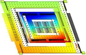
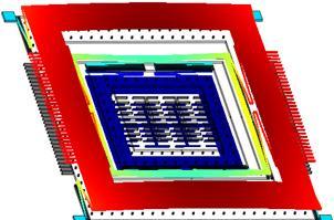
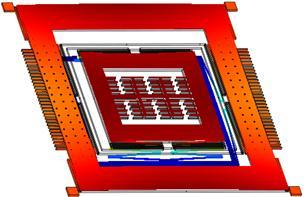
104 Table Electrostatically-actuated MetalMUMPS gyroscope mode shape comparison. Mode Shape Simulated (khz) Experimental (khz) Error (%) % % % Not Available Not Available % % 90
105 Due to the increased relative complexity of the electrostatically-actuated MetalMUMPS gyroscope, it has a high mode shape density making it difficult to differentiate between modes. Higher-energy modes typically overwhelm those with smaller amplitudes as well, which makes them difficult to identify Error Explanation There are several factors that can explain the discrepancies found between the simulated and experimental results. One source of error is the exclusion of damping from the simulated model. This is expected to reduce the resonant frequencies in each mode compared to the simulated eigenfrequencies. The damping factor is also expected to vary with each mode shape depending on the contribution of viscous shearing forces and pressure differentials across the vibrating element. An in-plane mode will be less damped compared to an out-of-plane mode because there will be a greater shear force and a smaller pressure differential due to the surface area in each plane. It is expected that the experimental in-plane resonant frequencies will be closer to the simulated values for this reason. The information contained in table 5-1 is agreeable with this theory. However, upon calculating the quality factors from the experimental data using equation 1.8 and determining the damping coefficients using equation 1.7, the damping coefficient, ζ, for each mode shape was determined to be much less than 0.1; therefore damping can be accurately neglected from the simulated model. The quality factors and damping coefficients for each experimentally determined resonant peak are shown in figures 1 and 2 in the appendix. The material properties from the COMSOL library and those of the gyroscopes can vary and cause a disparity between the simulated and experimental data. The material properties are also expected to be inconsistent within the gyroscope structure depending on imperfections and the size of the grain boundaries. The two significant properties that would affect the difference between the experimental and simulated models are density and Young s modulus. The values of 91
106 the properties are dependent on the type of fabrication method used and the thickness of the thin film. The range of values for the Young s modulus of nickel has been reported by various sources to be anywhere between 150GPa and 245GPa 21. Any deviation of the actual material properties from the default COMSOL properties is expected to shift the resonant frequencies that the mode shapes occur at. The values that were used in the simulations are contained in table 1 in the appendix, which were taken directly from the COMSOL material library. According to the analytical model, a Young s modulus of 245GPa, a difference of 12% between the simulated and experimental value, would result in a discrepancy of 5.8%. Therefore any difference in the actual value of the Young s modulus would not account for all the error reported in tables 5-1 and 5-2. The dimensions of the gyroscopes are also expected to vary between the simulated models and the prototypes. The CAD models, which were used for fabrication, were imported directly into COMSOL; the simulated and prototype dimensions are identical except for alterations made to the thermal gyroscope to simplify the structure and dimension variation due to fabrication tolerances. These variations are expected to change the spring and mass values for each element within the gyroscope s structure. The spring values are more susceptible to changes in the dimensions because of the relative thinness of the flexures. The thickness of MetalMUMPS structures can vary up to 20±10µm, which can result in large discrepancies between the actual device and the theoretical mass and spring matrices. 11 A thickness of 30µm would result in a discrepancy between the simulated and experimental results up to 50% according to the analytical model, which would account for all the error in the out-of-plane results. Two other common causes of dimensional error include slanted side-walls, an inherent limitation of the MetalMUMPS process, and mushrooming of the electroplated nickel. 92
107 Residual stresses may also be present within the structure after fabrication. They are not particularly significant in bottom-up fabrication processes such as electroplating but can still affect the resonant frequencies of a mechanical system. 93
108 5.3 Performance Analysis Thermally-Actuated MetalMUMPS Gyroscope Mode Matching The in-plane analysis in chapter 4 for the thermally-actuated gyroscope indicates that the driving and sensing modes are closely matched. The driving mode occurred at 6.0kHz and the sensing mode occurred at 5.98kHz. Having both modes directly coincide is ideal if the objective is to elicit the greatest response using the least amount of energy; however the system s performance is relatively unstable in this case. Fluctuations in temperature and pressure can affect the sensing mode s resonant frequency and change the magnitude of the response that will ultimately affect the output. It is expected that the thermally-actuated gyroscope will be highly dependent on environmental temperatures and pressures during operation, which will need to be compensated by additional circuitry. The sensitivity of environmental conditions can be tested by applying an angular velocity and changing the temperature and pressure then measuring the output. Sensitivity is one of the performance indicators of gyroscopic sensors Electrostatically-Actuated MetalMUMPS Gyroscope Predicted Mode Matching Experimental in-plane mode testing has not been performed; consequently the simulated data is used to predict the modal response of the electrostatically-actuated gyroscopes. Three in-plane modes were identified in the simulated model. At 1.6kHz the proof mass and decoupling frame vibrate in the driving direction, and at 1.9kHz the proof mass resonates in the sensing direction. The gyroscope is expected to have poor temperature and pressure sensitivity because of the high quality factor of the sensing and driving mode frequency response curves. The gyroscope also will not take advantage of mode coupling because of the relatively large difference in proximity between the driving and sensing modes. Also, the out-of-phase driving mode, estimated to occur at 2.316kHz, will negatively affect the performance. The velocity of the proof mass is reduced by 94
109 the out-of-phase motion, which will affect the response in the sensing direction; therefore excitation signals close to this frequency should be avoided during operation Electrostatically-Actuated SOI Gyroscope Predicted Mode Matching The simulated driving and sensing mode resonant frequencies was determined to be 2.159kHz and 3.298kHz respectively. The frequency span between both modes may be too great for the gyroscope to take advantage of mode matching; however it is difficult to speculate without knowing the quality factor of each peak. The driving response of the gyroscope will also be relatively small because of the large disparity between the driving and sensing modes Thermally-Actuated Gyroscope Power and Efficiency Electrical power tests and the amplitude response from the gyroscope, summarized in figure 4-8, are important to the viability of thermally-actuated gyroscope designs. A significant disadvantage of electrostatically-actuated designs is the high voltage requirement, which requires on-chip circuitry and can sometimes restrict design possibilities. Thermal actuators require much lower voltages that make them easily implemented with digital CMOS circuitry. The disadvantage of thermal actuators is their large power requirements compared to electrostatic actuators, which is evident in the power tests that were performed. The largest amplitude observed was 4.2µm, which required mW to achieve. Increasing the power only induced out-of-plane responses. Microprocessors cannot output this much current; however several adjustments can be made to drive the gyroscope with a microprocessor. Microprocessors are only capable of outputting square wave signals as opposed to the sinusoidal actuation signals were used during testing to drive the gyroscope. It was not possible to perform tests using a square wave actuation signal due to limitations of the testing equipment; however a square wave driving signal would be a better waveform to use because of its greater power 95
110 density, which would also elicit a faster response. Adjusting the voltage drop across the thermal actuator is one prerequisite for testing using a microprocessor. Currently, a 1.5V RMS drop is observed; most microprocessors output 5V. It would be more efficient if a 5V drop was observed; however the gyroscope would have to be designed and fabricated around these specifications. Future thermally-actuated gyroscopes could incorporate this in their design specifications to optimize the efficiency. The power requirements of the gyroscope would be further reduced by using on-chip circuitry. There is energy loss in the wires with the current testing setup that would be reduced if shorter interconnects were used. Also, the power used to elicit a peak-to-peak displacement of 4.2µm is not necessary. A smaller electrical current will also excite the proof mass in the sensing direction as well, albeit at a reduced response due to the decrease in driving velocity. Further testing is required to determine how low the driving current can be while still maintaining an acceptable output signal. 96
111 Chapter 6 Conclusion The objective was to determine and characterize the modal behaviour of three MEMS gyroscopic sensors using simulated models in COMSOL and through experimental methods. Each gyroscope had its own distinguishing features; one was a novel thermally-actuated design, another used an electrostatic actuation method, which was manufactured using the MetalMUMPS fabrication process and another was an out-of-plane SOI design. Simulated models were created for all three gyroscopes from CAD files to reduce the potential for dimensional error. Several mode shape resonant frequencies were solved for in each model, which were then used as predictions for the experimental PSV and PMA testing to help interpret the results. Experimental testing was then performed for the thermally-actuated gyroscope and electrostatic MetalMUMPS gyroscope. Static testing was performed first to identify the driving signal power requirements. The thermal actuator required a driving current of at least 150mA to elicit a significant response. Similarly, the electrostatic actuator required a 25V AC with 25V DC offset to actuate. Seventeen dynamic tests were performed to characterize the response of the thermal gyroscope at different driving currents. The maximum peak-to-peak displacement observed was 4.2µm at 225.4mA RMS current. Increasing the current provoked out-of-plane responses and reduced the in-plane displacement. The frequency response of the thermal actuator was determined similarly by measuring the amplitude of the displacement and varying the frequency. The frequency response of the in-plane sensing mode was also measured by using the parallel plate sensing fingers as actuators by applying a 40V AC driving signal. The natural frequency of the driving and sensing modes of the thermally-actuated gyroscope was experimentally 97
112 determined to be 6.0kHz and 5.98kHz respectively. Similarly, the driving and sensing mode resonant frequencies for the MetalMUMPS electrostatically-actuated gyroscope are 1.6kHz and 1.9kHz respectively. The out-of-plane mode shape resonant frequencies were found using an FFT. The results were compared to the eigenfrequencies found in the simulated solutions and the discrepancies were attributed to fabrication and material tolerances, residual stresses and the exclusion of damping from the simulated model. An analytical model as well as quality factors derived from the experimental results was used to determine the most significant contributor to the error that was observed. The fabrication and material tolerances were determined to be the most significant contributors to the error between the experimental and theoretical results. An analysis on each significant mode shape helped identify modes that may interfere with the sensing performance of the gyroscopes. Similarly, the locations of the natural frequencies of the driving and sensing modes were used to predict the response of the gyroscope from mode matching. 6.1 Future Work Recommendations The simulated models need additional work if they are to be useful for the fabrication of future gyroscope models. The inclusion of damping in a frequency response simulation would be useful for predicting the modal behaviour of the gyroscopes; however it will be difficult to derive an accurate viscous damping model that accounts for the variability in damping coefficients for each mode shape. Tweaking the material property settings, model dimensions and residual stresses in the current COMSOL models such that they closely match the experimental data will help with future simulations for other gyroscopes as well if the same settings are used. Completion of testing on the SOI electrostatically-actuated gyroscope would be useful for revising the simulations. 98
113 Circuitry for the capacitive sensing plates must be designed and connected as well in order to convert the capacitance to an output voltage for all gyroscopes. The significance of the modal behaviour of each gyroscope will be made explicit by measuring the performance indicators using rate table testing. Insight gained from these tests will be useful in designing future gyroscope devices. It is recommended that a new thermal-actuated gyroscope should be designed and fabricated to take advantage of the increased efficiency and ease-of-integration benefits of a thermal actuator that is intended to accept a 5V square wave driving signal. 6.2 Thesis Contribution All the simulated and experimental results were original work performed by the author. The gyroscopic sensors were designed by Rana Iqtidar Shakoor, a previous graduate student at Queen s University. 99
114 References 1 R. Feynman, There s Plenty of Room at the Bottom, Journal of Micromechanical Systems Vol. 1, No. 1, March 1992, pp M. Dahleh and W. Thomson, Theory of Vibration with Applications, 5 th Edition, Prentice-Hall Inc, 1998, ISBN X. 3 B. Zhang and D. Fang, Modeling and modification of the parallel plate variable MEMS capacitors considering deformation issue, Mechanism and Machine Theory, 44(4), 2009, pp R. Johnson, MEMS finds niche in space exploration, EE Times, W. Huang and G. Lu, Analysis of lateral instability of in-plane comb drive MEMS actuators based on a two-dimensional model, Sensors and Actuators A: Physical 113(1), 2004, pp J.-C. Chiou, Y.-J. Lin and C.-F. Kuo, Extending the traveling range with acascade electrostatic comb-drive actuator, J. Micromech. Microeng. 18 (2008) (7pp). 7 Lithography, 8 J. Ravnkilde, A. Yalcinkaya, L. Johansen and O. Hansen, Fabrication of electroplated nickel micromechanical comb resonators, Technical University of Denmark DTU, Electrochemical Society Proceedings Vol , pp J. Jahns and K. Brenner, Microoptics: From technology to applications, New York : Springer, O. Geschke, H. Klank, P. Telleman, Microsystem Engineering of Lab-on-a-Chip Devices, Ch. 6, Silicon and Cleanroom Processing (Lecture 2), Wiley-VCH, MetalMUMPs Design Handbook, Revision 2.0, MEMSCAP Inc. 12 Micragem Data Sheet, Micralyne Inc. 100
115 13 B. Bokenhorn and P. Greiff, A vibratory micromechanical gyroscope, Navigation and Control Conference, Minneapolis, MN, Aug , 1988, Technical Papers. Part 2 (A ). Washington, DC, American Institute of Aeronautics and Astronautics, 1988, p Roylance, L. M., and J. B. Angell, A Batch-Fabricated Silicon Accelerometer, IEEE Trans. Electron Devices, ED-26, 1979, pp K. Tanaka, Y. Mochida, S. Sugimoto, K. Moriya, T. Hasegawa, K. Atsuchi, and K. Ohwada, A micromachined vibrating gyroscope. Proc., Eighth IEEE Int. Conf. on Micro Electro Mechanical Systems (MEMS 95), Amsterdam, Netherlands, Jan. 1995, pp T. Juneau, A. P. Pisano, and J. H. Smith, Dual axis operation of a micromachined rate gyroscope Proc., IEEE 1997 Int. Conf. on Solid State Sensors and Actuators (Tranducers 97), Chicago, June 1997, pp Y. Mochida, M. Tamura, and K. Ohwada, A micromachined vibrating rate gyroscope with independent beams for the drive and detection modes. Proc. Twelfth IEEE Int. Conf. on Micro Electro Mechanical Systems (MEMS 99), Orlando, FL, Jan. 1999, pp C. Acar, A. M. Shkel Inherently Robust Micromachined Gyroscopes with 2-DoF Sense Mode Oscillator Journal of Microelectromechanical System, Vol 15, No.2, April 2006, pp S. Bazaz, M. Burnie, M. Hasan, Y. Lai and R. Shakoor, Electrothermally Actuated Resonant Rate Gyroscope Fabricated using the MetalMUMPs, unpublished. 20 Polytec Scanning Vibrometer: Theory Manual, Revision 8.4, Polytec Inc. 21 D.-C. Baek, T.-S. Park and S.-B. Lee, Measurement of Mechanical Properties of Electroplated Nickel Thin Film, Key Engineering Materials Vols , 2004, pp
116 Appendix Table Appendix-5-Error! Main Document Only. - Values for material properties used for simulation models. Material Young`s Modulus (GPa) Density (kg/m 3 ) Nickel Single-Crystal Silicon Table Appenix-5-Error! Main Document Only. - Thermally-actuated gyroscope dynamic testing results. SG P-P Volt. (V) Gyro P-P Volt. (V) Gyro RMS Volt. (V) RMS Current (ma) Gyro Power (mw) DC Current (ma) Peak-to- Peak (µm)


117 Figure Appendix- Error! Main Document Only. Experimentally calculated quality factors and damping coefficients of the thermally-actuated gyroscopic sensor. Figure Appendix- Error! Main Document Only. - Experimentally calculated quality factors and damping coefficients of the electrostatically-actuated MetalMUMPS gyroscopic sensor. 103
Institute for Electron Microscopy and Nanoanalysis Graz Centre for Electron Microscopy
 Institute for Electron Microscopy and Nanoanalysis Graz Centre for Electron Microscopy Micromechanics Ass.Prof. Priv.-Doz. DI Dr. Harald Plank a,b a Institute of Electron Microscopy and Nanoanalysis, Graz
MEMS Tuning-Fork Gyroscope Mid-Term Report Amanda Bristow Travis Barton Stephen Nary
 MEMS Tuning-Fork Gyroscope Mid-Term Report Amanda Bristow Travis Barton Stephen Nary Abstract MEMS based gyroscopes have gained in popularity for use as rotation rate sensors in commercial products like
EE C245 / ME C218 INTRODUCTION TO MEMS DESIGN FALL 2009 PROBLEM SET #7. Due (at 7 p.m.): Thursday, Dec. 10, 2009, in the EE C245 HW box in 240 Cory.
: Thursday, Dec. 10, 2009, in the EE C245 HW box in 240 Cory.") Issued: Thursday, Nov. 24, 2009 PROBLEM SET #7 Due (at 7 p.m.): Thursday, Dec. 10, 2009, in the EE C245 HW box in 240 Cory. 1. Gyroscopes are inertial sensors that measure rotation rate, which is an extremely
Issued: Thursday, Nov. 24, 2009 PROBLEM SET #7 Due (at 7 p.m.): Thursday, Dec. 10, 2009, in the EE C245 HW box in 240 Cory. 1. Gyroscopes are inertial sensors that measure rotation rate, which is an extremely
Design and characterization of in-plane MEMS yaw rate sensor
 Sādhanā Vol. 34, Part 4, August 2009, pp. 633 642. Printed in India Design and characterization of in-plane MEMS yaw rate sensor K P VENKATESH, NISHAD PATIL, ASHOK KUMAR PANDEY and RUDRA PRATAP CranesSci
1. Narrative Overview Questions
 Homework 4 Due Nov. 16, 010 Required Reading: Text and Lecture Slides on Downloadable from Course WEB site: http://courses.washington.edu/overney/nme498.html 1. Narrative Overview Questions Question 1
UNIT 3. By: Ajay Kumar Gautam Asst. Prof. Dev Bhoomi Institute of Technology & Engineering, Dehradun
 UNIT 3 By: Ajay Kumar Gautam Asst. Prof. Dev Bhoomi Institute of Technology & Engineering, Dehradun 1 Syllabus Lithography: photolithography and pattern transfer, Optical and non optical lithography, electron,
b. The displacement of the mass due to a constant acceleration a is x=
 EE147/247A Final, Fall 2013 Page 1 /35 2 /55 NO CALCULATORS, CELL PHONES, or other electronics allowed. Show your work, and put final answers in the boxes provided. Use proper units in all answers. 1.
DESIGN AND FABRICATION OF THE MICRO- ACCELEROMETER USING PIEZOELECTRIC THIN FILMS
 DESIGN AND FABRICATION OF THE MICRO- ACCELEROMETER USING PIEZOELECTRIC THIN FILMS JYH-CHENG YU and FU-HSIN LAI Department of Mechanical Engineering National Taiwan University of Science and Technology
Four Degrees-of-Freedom Micromachined Gyroscope
 Microsystems Laboratory Technical Report Four Degrees-of-Freedom Micromachined Gyroscope Cenk Acar 23 October 2001 Technical Report No: MSL-01003 cfl2001 Cenk Acar Contents Contents List of Figures Abstract
UNIVERSITY OF CALIFORNIA College of Engineering Department of Electrical Engineering and Computer Sciences. Fall Exam 1
 UNIVERSITY OF CALIFORNIA College of Engineering Department of Electrical Engineering and Computer Sciences EECS 143 Fall 2008 Exam 1 Professor Ali Javey Answer Key Name: SID: 1337 Closed book. One sheet
EE C245 ME C218 Introduction to MEMS Design Fall 2007
 EE C245 ME C218 Introduction to MEMS Design Fall 2007 Prof. Clark T.-C. Nguyen Dept. of Electrical Engineering & Computer Sciences University of California at Berkeley Berkeley, CA 94720 Lecture 12: Mechanics
Etching Issues - Anisotropy. Dry Etching. Dry Etching Overview. Etching Issues - Selectivity
 Etching Issues - Anisotropy Dry Etching Dr. Bruce K. Gale Fundamentals of Micromachining BIOEN 6421 EL EN 5221 and 6221 ME EN 5960 and 6960 Isotropic etchants etch at the same rate in every direction mask
EE C245 / ME C218 INTRODUCTION TO MEMS DESIGN FALL 2011 C. Nguyen PROBLEM SET #7. Table 1: Gyroscope Modeling Parameters
 Issued: Wednesday, Nov. 23, 2011. PROBLEM SET #7 Due (at 7 p.m.): Thursday, Dec. 8, 2011, in the EE C245 HW box in 240 Cory. 1. Gyroscopes are inertial sensors that measure rotation rate, which is an extremely
Foundations of MEMS. Chang Liu. McCormick School of Engineering and Applied Science Northwestern University. International Edition Contributions by
 Foundations of MEMS Second Edition Chang Liu McCormick School of Engineering and Applied Science Northwestern University International Edition Contributions by Vaishali B. Mungurwadi B. V. Bhoomaraddi
HSG-IMIT Application AG
 B4.1 Acceleration Sensors IP-Blocks for MEMS Foundry Surface Micromachining Process R. Knechtel, S. Dempwolf S. Hering X-FAB Semiconductor Foundries AG Haarberstraße 67 99097 Erfurt / Germany T. Link J.
Objectives. Fundamentals of Dynamics: Module 9 : Robot Dynamics & controls. Lecture 31 : Robot dynamics equation (LE & NE methods) and examples
 and examples") \ Module 9 : Robot Dynamics & controls Lecture 31 : Robot dynamics equation (LE & NE methods) and examples Objectives In this course you will learn the following Fundamentals of Dynamics Coriolis component
\ Module 9 : Robot Dynamics & controls Lecture 31 : Robot dynamics equation (LE & NE methods) and examples Objectives In this course you will learn the following Fundamentals of Dynamics Coriolis component
LECTURE 5 SUMMARY OF KEY IDEAS
 LECTURE 5 SUMMARY OF KEY IDEAS Etching is a processing step following lithography: it transfers a circuit image from the photoresist to materials form which devices are made or to hard masking or sacrificial
SUPPLEMENTARY INFORMATION
 In the format provided by the authors and unedited. DOI: 10.1038/NPHOTON.2016.254 Measurement of non-monotonic Casimir forces between silicon nanostructures Supplementary information L. Tang 1, M. Wang
Introduction to Photolithography
 http://www.ichaus.de/news/72 Introduction to Photolithography Photolithography The following slides present an outline of the process by which integrated circuits are made, of which photolithography is
Self-study problems and questions Processing and Device Technology, FFF110/FYSD13
 Self-study problems and questions Processing and Device Technology, FFF110/FYSD13 Version 2016_01 In addition to the problems discussed at the seminars and at the lectures, you can use this set of problems
Regents of the University of California
 Deep Reactive-Ion Etching (DRIE) DRIE Issues: Etch Rate Variance The Bosch process: Inductively-coupled plasma Etch Rate: 1.5-4 μm/min Two main cycles in the etch: Etch cycle (5-15 s): SF 6 (SF x+ ) etches
EECS C245 ME C218 Midterm Exam
 University of California at Berkeley College of Engineering EECS C245 ME C218 Midterm Eam Fall 2003 Prof. Roger T. Howe October 15, 2003 Dr. Thara Srinivasan Guidelines Your name: SOLUTIONS Circle your
CHAPTER 6: Etching. Chapter 6 1
 Chapter 6 1 CHAPTER 6: Etching Different etching processes are selected depending upon the particular material to be removed. As shown in Figure 6.1, wet chemical processes result in isotropic etching
Metal Deposition. Filament Evaporation E-beam Evaporation Sputter Deposition
 Metal Deposition Filament Evaporation E-beam Evaporation Sputter Deposition 1 Filament evaporation metals are raised to their melting point by resistive heating under vacuum metal pellets are placed on
EE C247B / ME C218 INTRODUCTION TO MEMS DESIGN SPRING 2016 C. NGUYEN PROBLEM SET #4
 Issued: Wednesday, March 4, 2016 PROBLEM SET #4 Due: Monday, March 14, 2016, 8:00 a.m. in the EE C247B homework box near 125 Cory. 1. This problem considers bending of a simple cantilever and several methods
ETCHING Chapter 10. Mask. Photoresist
 ETCHING Chapter 10 Mask Light Deposited Substrate Photoresist Etch mask deposition Photoresist application Exposure Development Etching Resist removal Etching of thin films and sometimes the silicon substrate
Y. C. Lee. Micro-Scale Engineering I Microelectromechanical Systems (MEMS)
") Micro-Scale Engineering I Microelectromechanical Systems (MEMS) Y. C. Lee Department of Mechanical Engineering University of Colorado Boulder, CO 80309-0427 leeyc@colorado.edu January 15, 2014 1 Contents
Micro-Scale Engineering I Microelectromechanical Systems (MEMS) Y. C. Lee Department of Mechanical Engineering University of Colorado Boulder, CO 80309-0427 leeyc@colorado.edu January 15, 2014 1 Contents
DEPOSITION OF THIN TiO 2 FILMS BY DC MAGNETRON SPUTTERING METHOD
 Chapter 4 DEPOSITION OF THIN TiO 2 FILMS BY DC MAGNETRON SPUTTERING METHOD 4.1 INTRODUCTION Sputter deposition process is another old technique being used in modern semiconductor industries. Sputtering
EE C247B / ME C218 INTRODUCTION TO MEMS DESIGN SPRING 2014 C. Nguyen PROBLEM SET #4
 Issued: Wednesday, Mar. 5, 2014 PROBLEM SET #4 Due (at 9 a.m.): Tuesday Mar. 18, 2014, in the EE C247B HW box near 125 Cory. 1. Suppose you would like to fabricate the suspended cross beam structure below
Integrating MEMS Electro-Static Driven Micro-Probe and Laser Doppler Vibrometer for Non-Contact Vibration Mode SPM System Design
 Tamkang Journal of Science and Engineering, Vol. 12, No. 4, pp. 399 407 (2009) 399 Integrating MEMS Electro-Static Driven Micro-Probe and Laser Doppler Vibrometer for Non-Contact Vibration Mode SPM System
SUPPLEMENTARY NOTES Supplementary Note 1: Fabrication of Scanning Thermal Microscopy Probes
 SUPPLEMENTARY NOTES Supplementary Note 1: Fabrication of Scanning Thermal Microscopy Probes Fabrication of the scanning thermal microscopy (SThM) probes is summarized in Supplementary Fig. 1 and proceeds
EE 527 MICROFABRICATION. Lecture 24 Tai-Chang Chen University of Washington
 EE 527 MICROFABRICATION Lecture 24 Tai-Chang Chen University of Washington EDP ETCHING OF SILICON - 1 Ethylene Diamine Pyrocatechol Anisotropy: (100):(111) ~ 35:1 EDP is very corrosive, very carcinogenic,
Fabrication Technology, Part I
 EEL5225: Principles of MEMS Transducers (Fall 2004) Fabrication Technology, Part I Agenda: Microfabrication Overview Basic semiconductor devices Materials Key processes Oxidation Thin-film Deposition Reading:
Etching: Basic Terminology
 Lecture 7 Etching Etching: Basic Terminology Introduction : Etching of thin films and sometimes the silicon substrate are very common process steps. Usually selectivity, and directionality are the first
December 1999 FINAL TECHNICAL REPORT 1 Mar Mar 98
 REPORT DOCUMENTATION PAGE AFRL-SR- BL_TR " Public reporting burden for this collection of information is estimated to average 1 hour per response, including the time for reviewing instruct the collection
Design and Analysis of dual Axis MEMS Capacitive Accelerometer
 International Journal of Electronics Engineering Research. ISSN 0975-6450 Volume 9, Number 5 (2017) pp. 779-790 Research India Publications http://www.ripublication.com Design and Analysis of dual Axis
Kavli Workshop for Journalists. June 13th, CNF Cleanroom Activities
 Kavli Workshop for Journalists June 13th, 2007 CNF Cleanroom Activities Seeing nm-sized Objects with an SEM Lab experience: Scanning Electron Microscopy Equipment: Zeiss Supra 55VP Scanning electron microscopes
Silicon Capacitive Accelerometers. Ulf Meriheinä M.Sc. (Eng.) Business Development Manager VTI TECHNOLOGIES
 Business Development Manager VTI TECHNOLOGIES") Silicon Capacitive Accelerometers Ulf Meriheinä M.Sc. (Eng.) Business Development Manager VTI TECHNOLOGIES 1 Measuring Acceleration The acceleration measurement is based on Newton s 2nd law: Let the acceleration
Silicon Capacitive Accelerometers Ulf Meriheinä M.Sc. (Eng.) Business Development Manager VTI TECHNOLOGIES 1 Measuring Acceleration The acceleration measurement is based on Newton s 2nd law: Let the acceleration
Lecture 18: Microfluidic MEMS, Applications
 MECH 466 Microelectromechanical Systems University of Victoria Dept. of Mechanical Engineering Lecture 18: Microfluidic MEMS, Applications 1 Overview Microfluidic Electrokinetic Flow Basic Microfluidic
IC Fabrication Technology
 IC Fabrication Technology * History: 1958-59: J. Kilby, Texas Instruments and R. Noyce, Fairchild * Key Idea: batch fabrication of electronic circuits n entire circuit, say 10 7 transistors and 5 levels
Lecture 6 Plasmas. Chapters 10 &16 Wolf and Tauber. ECE611 / CHE611 Electronic Materials Processing Fall John Labram 1/68
 Lecture 6 Plasmas Chapters 10 &16 Wolf and Tauber 1/68 Announcements Homework: Homework will be returned to you on Thursday (12 th October). Solutions will be also posted online on Thursday (12 th October)
Design and Simulation of Comb Drive Capacitive Accelerometer by Using MEMS Intellisuite Design Tool
 Design and Simulation of Comb Drive Capacitive Accelerometer by Using MEMS Intellisuite Design Tool Gireesh K C 1, Harisha M 2, Karthick Raj M 3, Karthikkumar M 4, Thenmoli M 5 UG Students, Department
How Does a Microcantilever Work?
 How Does a Cantilever Work? Participant Guide Description and Estimated Time to Complete The microcantilever is a widely used component in microsystems devices or microelectromechanical systems (MEMS).
Kurukshetra University INDIA
 American International Journal of Research in Science, Technology, Engineering & Mathematics Available online at http://www.iasir.net ISSN (Print): 2328-3491, ISSN (Online): 2328-3580, ISSN (CD-ROM): 2328-3629
EE C245 ME C218 Introduction to MEMS Design
 EE C245 ME C218 Introduction to MEMS Design Fall 2007 Prof. Clark T.-C. Nguyen Dept. of Electrical Engineering & Computer Sciences University of California at Berkeley Berkeley, CA 94720 Lecture 21: Gyros
MODELING OF T-SHAPED MICROCANTILEVER RESONATORS. Margarita Narducci, Eduard Figueras, Isabel Gràcia, Luis Fonseca, Joaquin Santander, Carles Cané
 Stresa, Italy, 5-7 April 007 MODELING OF T-SHAPED MICROCANTILEVER RESONATORS Margarita Narducci, Eduard Figueras, Isabel Gràcia, Luis Fonseca, Joaquin Santander, Carles Centro Nacional de Microelectrónica
CHAPTER 5 FIXED GUIDED BEAM ANALYSIS
 77 CHAPTER 5 FIXED GUIDED BEAM ANALYSIS 5.1 INTRODUCTION Fixed guided clamped and cantilever beams have been designed and analyzed using ANSYS and their performance were calculated. Maximum deflection
Optimizing micromechanical force detectors for measuring. magnetization at high magnetic fields
 Abstract Optimizing micromechanical force detectors for measuring magnetization at high magnetic fields Jeremy Paster University of Florida July 30, 2008 MEMS devices prove to be advantageous in magnetometry.
Table of Content. Mechanical Removing Techniques. Ultrasonic Machining (USM) Sputtering and Focused Ion Beam Milling (FIB)
 Sputtering and Focused Ion Beam Milling (FIB)") Table of Content Mechanical Removing Techniques Ultrasonic Machining (USM) Sputtering and Focused Ion Beam Milling (FIB) Ultrasonic Machining In ultrasonic machining (USM), also called ultrasonic grinding,
Table of Content Mechanical Removing Techniques Ultrasonic Machining (USM) Sputtering and Focused Ion Beam Milling (FIB) Ultrasonic Machining In ultrasonic machining (USM), also called ultrasonic grinding,
Tunable MEMS Capacitor for RF Applications
 Tunable MEMS Capacitor for RF Applications Shriram H S *1, Tushar Nimje 1, Dhruv Vakharia 1 1 BITS Pilani, Rajasthan, India *1167, 1 st Main, 2 nd Block, BEL Layout, Vidyaranyapura, Bangalore 560097; email:
Lecture 150 Basic IC Processes (10/10/01) Page ECE Analog Integrated Circuits and Systems P.E. Allen
 Page ECE Analog Integrated Circuits and Systems P.E. Allen") Lecture 150 Basic IC Processes (10/10/01) Page 1501 LECTURE 150 BASIC IC PROCESSES (READING: TextSec. 2.2) INTRODUCTION Objective The objective of this presentation is: 1.) Introduce the fabrication of
Lecture 150 Basic IC Processes (10/10/01) Page 1501 LECTURE 150 BASIC IC PROCESSES (READING: TextSec. 2.2) INTRODUCTION Objective The objective of this presentation is: 1.) Introduce the fabrication of
Development and Characterization of High Frequency Bulk Mode Resonators
 Excerpt from the Proceedings of the COMSOL Conference 008 Hannover Development and Characterization of High Frequency Bulk Mode Resonators Hossein Pakdast 1*, Zachary James Davis 1 1 DTU Nanotech, Technical
Design of a MEMS Capacitive Comb-drive Accelerometer
 Design of a MEMS Capacitive Comb-drive Accelerometer Tolga Kaya* 1, Behrouz Shiari 2, Kevin Petsch 1 and David Yates 2 1 Central Michigan University, 2 University of Michigan * kaya2t@cmich.edu Abstract:
Chapter 3 Engineering Science for Microsystems Design and Fabrication
 Lectures on MEMS and MICROSYSTEMS DESIGN and MANUFACTURE Chapter 3 Engineering Science for Microsystems Design and Fabrication In this Chapter, we will present overviews of the principles of physical and
Microfabrication for MEMS: Part I
 Microfabrication for MEMS: Part I Carol Livermore Massachusetts Institute of Technology * With thanks to Steve Senturia, from whose lecture notes some of these materials are adapted. CL: 6.777J/2.372J
Dynamization evolution of Dry Etch Tools in Semiconductor Device Fabrication Gordon Cameron Intel Corp (November 2005)
") Dynamization evolution of Dry Etch Tools in Semiconductor Device Fabrication Gordon Cameron Intel Corp (November 2005) Abstract Engineering Systems follow recognized trends of evolution; the main parameters
Dynamization evolution of Dry Etch Tools in Semiconductor Device Fabrication Gordon Cameron Intel Corp (November 2005) Abstract Engineering Systems follow recognized trends of evolution; the main parameters
Supplementary Figure 1 Detailed illustration on the fabrication process of templatestripped
 Supplementary Figure 1 Detailed illustration on the fabrication process of templatestripped gold substrate. (a) Spin coating of hydrogen silsesquioxane (HSQ) resist onto the silicon substrate with a thickness
4FNJDPOEVDUPS 'BCSJDBUJPO &UDI
 2010.5.4 1 Major Fabrication Steps in CMOS Process Flow UV light oxygen Silicon dioxide Silicon substrate Oxidation (Field oxide) photoresist Photoresist Coating Mask exposed photoresist Mask-Wafer Exposed
TMT4320 Nanomaterials November 10 th, Thin films by physical/chemical methods (From chapter 24 and 25)
") 1 TMT4320 Nanomaterials November 10 th, 2015 Thin films by physical/chemical methods (From chapter 24 and 25) 2 Thin films by physical/chemical methods Vapor-phase growth (compared to liquid-phase growth)
1 TMT4320 Nanomaterials November 10 th, 2015 Thin films by physical/chemical methods (From chapter 24 and 25) 2 Thin films by physical/chemical methods Vapor-phase growth (compared to liquid-phase growth)
CHAPTER 4 DESIGN AND ANALYSIS OF CANTILEVER BEAM ELECTROSTATIC ACTUATORS
 61 CHAPTER 4 DESIGN AND ANALYSIS OF CANTILEVER BEAM ELECTROSTATIC ACTUATORS 4.1 INTRODUCTION The analysis of cantilever beams of small dimensions taking into the effect of fringing fields is studied and
Supplementary Information Our InGaN/GaN multiple quantum wells (MQWs) based one-dimensional (1D) grating structures
 based one-dimensional (1D) grating structures") Polarized white light from hybrid organic/iii-nitrides grating structures M. Athanasiou, R. M. Smith, S. Ghataora and T. Wang* Department of Electronic and Electrical Engineering, University of Sheffield,
Polarized white light from hybrid organic/iii-nitrides grating structures M. Athanasiou, R. M. Smith, S. Ghataora and T. Wang* Department of Electronic and Electrical Engineering, University of Sheffield,
AC : MEMS FABRICATION AS A MULTIDISCIPLINARY LABORATORY
 AC 2007-524: MEMS FABRICATION AS A MULTIDISCIPLINARY LABORATORY Todd Kaiser, Montana State University Andrew Lingley, Montana State University Matt Leone, Montana State University Brad Pierson, Montana
Film Deposition Part 1
 1 Film Deposition Part 1 Chapter 11 : Semiconductor Manufacturing Technology by M. Quirk & J. Serda Spring Semester 2013 Saroj Kumar Patra Semidonductor Manufacturing Technology, Norwegian University of
E SC 412 Nanotechnology: Materials, Infrastructure, and Safety Wook Jun Nam
 E SC 412 Nanotechnology: Materials, Infrastructure, and Safety Wook Jun Nam Lecture 10 Outline 1. Wet Etching/Vapor Phase Etching 2. Dry Etching DC/RF Plasma Plasma Reactors Materials/Gases Etching Parameters
Nanostructures Fabrication Methods
 Nanostructures Fabrication Methods bottom-up methods ( atom by atom ) In the bottom-up approach, atoms, molecules and even nanoparticles themselves can be used as the building blocks for the creation of
Variable Capacitance Accelerometers: Design and Applications
 Variable Capacitance Accelerometers: Design and Applications Micromachined silicon variable-capacitance accelerometers are designed for easy manufacture and demanding applications. Tom Connolly, Endevco
MEMS INERTIAL POWER GENERATORS FOR BIOMEDICAL APPLICATIONS
 MEMS INERTIAL POWER GENERATORS FOR BIOMEDICAL APPLICATIONS P. MIAO, P. D. MITCHESON, A. S. HOLMES, E. M. YEATMAN, T. C. GREEN AND B. H. STARK Department of Electrical and Electronic Engineering, Imperial
EE C245 ME C218 Introduction to MEMS Design Fall 2007
 EE C245 ME C218 Introduction to MEMS Design Fall 2007 Prof. Clark T.-C. Nguyen Dept. of Electrical Engineering & Computer Sciences University of California at Berkeley Berkeley, CA 94720 Lecture 11: Bulk
Lithography and Etching
 Lithography and Etching Victor Ovchinnikov Chapters 8.1, 8.4, 9, 11 Previous lecture Microdevices Main processes: Thin film deposition Patterning (lithography) Doping Materials: Single crystal (monocrystal)
DQN Positive Photoresist
 UNIVESITY OF CALIFONIA, BEKELEY BEKELEY DAVIS IVINE LOS ANGELES IVESIDE SAN DIEGO SAN FANCISCO SANTA BABAA SANTA CUZ DEPATMENT OF BIOENGINEEING 94720-1762 BioE 121 Midterm #1 Solutions BEKELEY, CALIFONIA
Nanotechnology Fabrication Methods.
 Nanotechnology Fabrication Methods. 10 / 05 / 2016 1 Summary: 1.Introduction to Nanotechnology:...3 2.Nanotechnology Fabrication Methods:...5 2.1.Top-down Methods:...7 2.2.Bottom-up Methods:...16 3.Conclusions:...19
Transactions on the Built Environment vol 12, 1995 WIT Press, ISSN
 Transactions on the Built Environment vol 12, 1995 WIT Press, www.witpress.com, ISSN 1743-359 Design and analysis of a resonant gyroscope suitable for fabrication using the LIGA process L. Yao, E. Chowanietz,
Keywords. 1=magnetron sputtering, 2= rotatable cathodes, 3=substrate temperature, 4=anode. Abstract
 Managing Anode Effects and Substrate Heating from Rotatable Sputter Targets. F. Papa*, V. Bellido-Gonzalez**, Alex Azzopardi**, Dr. Dermot Monaghan**, *Gencoa Technical & Business Support in US, Davis,
There's Plenty of Room at the Bottom
 There's Plenty of Room at the Bottom 12/29/1959 Feynman asked why not put the entire Encyclopedia Britannica (24 volumes) on a pin head (requires atomic scale recording). He proposed to use electron microscope
Lecture 0: Introduction
 Lecture 0: Introduction Introduction q Integrated circuits: many transistors on one chip q Very Large Scale Integration (VLSI): bucketloads! q Complementary Metal Oxide Semiconductor Fast, cheap, low power
Introduction to Plasma
 What is a plasma? The fourth state of matter A partially ionized gas How is a plasma created? Energy must be added to a gas in the form of: Heat: Temperatures must be in excess of 4000 O C Radiation Electric
2.76/2.760 Multiscale Systems Design & Manufacturing
 2.76/2.760 Multiscale Systems Design & Manufacturing Fall 2004 MOEMS Devices for Optical communications system Switches and micromirror for Add/drops Diagrams removed for copyright reasons. MOEMS MEMS
Finite Element Analysis of Piezoelectric Cantilever
 Finite Element Analysis of Piezoelectric Cantilever Nitin N More Department of Mechanical Engineering K.L.E S College of Engineering and Technology, Belgaum, Karnataka, India. Abstract- Energy (or power)
SCME KIT OVERVIEW. Rainbow Wafer Kit
 SCME KIT OVERVIEW Rainbow Wafer Kit Micro Nano Conference I - 2011 Objectives of Each Kit The SCME kits are designed to work both as a stand-alone activity as well as to support the materials introduced
DESIGN AND ANALYSIS OF ROTATION RATE SENSOR. Modeling of vibratory MEMs Gyroscope
 DESIGN AND ANALYSIS OF ROTATION RATE SENSOR Modeling of vibratory MEMs Gyroscope 1 Priya.P.Shreshtha & 2 Sushas S.Mohite 1 Mechanical Department, Rajaram Bapu institute of Technology Islampur, Dist. Sangli,
Contactless Excitation of MEMS Resonant Sensors by Electromagnetic Driving
 Presented at the COMSOL Conference 2009 Milan University of Brescia Department of Electronics for Automation Contactless Excitation of MEMS Resonant Sensors by Electromagnetic Driving Marco Baù, VF V.
Resistance Thermometry based Picowatt-Resolution Heat-Flow Calorimeter
 Resistance Thermometry based Picowatt-Resolution Heat-Flow Calorimeter S. Sadat 1, E. Meyhofer 1 and P. Reddy 1, 1 Department of Mechanical Engineering, University of Michigan, Ann Arbor, 48109 Department
Design And Analysis of Microcantilevers With Various Shapes Using COMSOL Multiphysics Software
 Design And Analysis of Microcantilevers With Various Shapes Using COMSOL Multiphysics Software V. Mounika Reddy 1, G.V.Sunil Kumar 2 1,2 Department of Electronics and Instrumentation Engineering, Sree
Wet and Dry Etching. Theory
 Wet and Dry Etching Theory 1. Introduction Etching techniques are commonly used in the fabrication processes of semiconductor devices to remove selected layers for the purposes of pattern transfer, wafer
Thin Wafer Handling Challenges and Emerging Solutions
 1 Thin Wafer Handling Challenges and Emerging Solutions Dr. Shari Farrens, Mr. Pete Bisson, Mr. Sumant Sood and Mr. James Hermanowski SUSS MicroTec, 228 Suss Drive, Waterbury Center, VT 05655, USA 2 Thin
DEVELOPMENT OF A MEMS REPULSIVE ACTUATOR FOR LARGE OUT-OF-PLANE FORCE
 DEVELOPMENT OF A MEMS REPULSIVE ACTUATOR FOR LARGE OUT-OF-PLANE FORCE by Imran Khan A thesis submitted in conformity with the requirements for the degree of Masters of Applied Science Graduate Department
7. CONCLUSIONS & SCOPE
 7. CONCLUSIONS & SCOPE ENERGY harvesting is a critical technology for the expansion of self-governing, self-powered electronic devices. As the energy requirements of low-power electronics reduction, the
Outline. 4 Mechanical Sensors Introduction General Mechanical properties Piezoresistivity Piezoresistive Sensors Capacitive sensors Applications
 Sensor devices Outline 4 Mechanical Sensors Introduction General Mechanical properties Piezoresistivity Piezoresistive Sensors Capacitive sensors Applications Introduction Two Major classes of mechanical
Simple piezoresistive accelerometer
 Simple piezoresistive pressure sensor Simple piezoresistive accelerometer Simple capacitive accelerometer Cap wafer C(x)=C(x(a)) Cap wafer may be micromachined silicon, pyrex, Serves as over-range protection,
Introduction to Actuators PK
 Introduction to Actuators Primary Knowledge Participant Guide Description and Estimated Time to Complete This learning module is one of three SCME modules that discuss the types of components found in
Dept. of Electrical & Computer Engineering, Dept. of Mechanical Engineering University of Bridgeport, Bridgeport, CT /08/2015
 Design and Analysis of Three DOF Piezoelectric Vibration Energy Harvester Ravi Teja Purra Reddy, Xingguo Xiong, Junling Hu Dept. of Electrical & Computer Engineering, Dept. of Mechanical Engineering University
Microstructure cantilever beam for current measurement
 264 South African Journal of Science 105 July/August 2009 Research Articles Microstructure cantilever beam for current measurement HAB Mustafa and MTE Khan* Most microelectromechanical systems (MEMS) sensors
SENSOR DEVICES MECHANICAL SENSORS
 SENSOR DEVICES MECHANICAL SENSORS OUTLINE 4 Mechanical Sensors Introduction General mechanical properties Piezoresistivity Piezoresistive sensors Capacitive sensors Applications INTRODUCTION MECHANICAL
Electromagnetics in COMSOL Multiphysics is extended by add-on Modules
 AC/DC Module Electromagnetics in COMSOL Multiphysics is extended by add-on Modules 1) Start Here 2) Add Modules based upon your needs 3) Additional Modules extend the physics you can address 4) Interface
Asymmetrical heating behavior of doped Si channels in bulk silicon and in silicon-on-insulator under high current stress
 JOURNAL OF APPLIED PHYSICS VOLUME 86, NUMBER 12 15 DECEMBER 1999 Asymmetrical heating behavior of doped Si channels in bulk silicon and in silicon-on-insulator under high current stress C. N. Liao, a)
Design and fabrication of multi-dimensional RF MEMS variable capacitors
 University of South Florida Scholar Commons Graduate Theses and Dissertations Graduate School 2003 Design and fabrication of multi-dimensional RF MEMS variable capacitors Hariharasudhan T. Kannan University
Case Study of Electronic Materials Packaging with Poor Metal Adhesion and the Process for Performing Root Cause Failure Analysis
 Case Study of Electronic Materials Packaging with Poor Metal Adhesion and the Process for Performing Root Cause Failure Analysis Dr. E. A. Leone BACKGRUND ne trend in the electronic packaging industry
Nano-mechatronics. Presented by: György BudaváriSzabó (X0LY4M)
") Nano-mechatronics Presented by: György BudaváriSzabó (X0LY4M) Nano-mechatronics Nano-mechatronics is currently used in broader spectra, ranging from basic applications in robotics, actuators, sensors,
Nano-mechatronics Presented by: György BudaváriSzabó (X0LY4M) Nano-mechatronics Nano-mechatronics is currently used in broader spectra, ranging from basic applications in robotics, actuators, sensors,
EE 527 MICROFABRICATION. Lecture 25 Tai-Chang Chen University of Washington
 EE 527 MICROFABRICATION Lecture 25 Tai-Chang Chen University of Washington ION MILLING SYSTEM Kaufmann source Use e-beam to strike plasma A magnetic field applied to increase ion density Drawback Low etch
Design and Simulation of A MEMS Based Horseshoe Shaped Low Current Lorentz Deformable Mirror (LCL-DM).
.") Design and Simulation of A MEMS Based Horseshoe Shaped Low Current Lorentz Deformable Mirror (LCL-DM). Byoungyoul Park 1, Tao Chen 1, Cyrus Shafai 1 1 Electrical and Computer Engineering, University of
Design and Simulation of A MEMS Based Horseshoe Shaped Low Current Lorentz Deformable Mirror (LCL-DM). Byoungyoul Park 1, Tao Chen 1, Cyrus Shafai 1 1 Electrical and Computer Engineering, University of