Non-Destructive Contact Resistivity Measurements on Industrial Solar Cells
|
|
|
- Lambert Wade
- 6 years ago
- Views:
Transcription
: Kristopher O.")

1 Non-Destructive Contact Resistivity Measurements on Industrial Solar Cells University of Central Florida (UCF): Kristopher O. Davis, Geoffrey Gregory Foshan University, Gonda Electronic Technology: Zhihao Yang BrightSpot Automation: Andrew Gabor, Andrew Anselmo, Rob Janoch


2 Contact Resistivity Structures Linear variable spaced transfer length method (TLM) Linear equivalently spaced TLM (i.e., ladder) Circular TLM (ctlm) Schroder DK. Semiconductor Material and Device Characterization (1990). 1


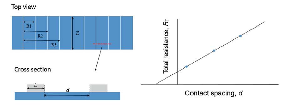
3 Linear TLM Guo, S., et al., Solar Energy, W f 2
.")
4 ctlm ctlm structures have a big advantage over linear TLM it s nondestructive Because of current flow being restricted between the inner and outer rings, no physical isolation of the test structure is required Schroder DK. Semiconductor Material and Device Characterization (1990). 3


5 Non-Destructive Contact Resistivity on Industrial Cells With BrightSpot Automation, we ve co-developed a non-destructive using circular TLM s hidden in the busbars BrightSpot Automation now builds a semi-automated tool, the ContactSpot- PRO, to implement this measurement G. Gregory, et al., 44 th IEEE PVSC,
 measured Initially curious about potential voltage drop around thinner outer rings")

6 ctlm Test Structure Designs Influence of the outer ring thickness on the total resistance (R T ) measured Initially curious about potential voltage drop around thinner outer rings Ultimately, thicker (top) and thinner (bottom) busbars yield same result, indicating voltage drop for thin outer rings is not an issue G. Gregory, et al., 44 th IEEE PVSC,
 Adding a fourth current probe only slightly reduced R T ( 2%) ContactSpot-PRO probe head designed with multiple current probes to minimize added metal")
7 Contact Probing Special attention was given to the effect of metal resistance on the measurement results Adding a third current probe, reduced R T significantly ( 35%) Adding a fourth current probe only slightly reduced R T ( 2%) ContactSpot-PRO probe head designed with multiple current probes to minimize added metal resistance 6

 7.72 Error in ρ c 35.6% % Error in ρ c 54.4% ctual R sheet (Ω/ ) 125.0 Actual R sheet (Ω/ ) 125.0 easured R sheet (Ω/ ) 121.3 Measured R sheet (Ω/ ) 116.")
8 Dimension Measurements Measurement of actual ctlm dimensions required due to variation from wafer-to-wafer and structure-to-structure ContactSpot-PRO Vision Sy Small errors in the gap distance can yield large error in R sheet and even larger error in ρ c Camera and image processing software used in the ContactSpot-PRO allow for real time measurent of all test structures measured Optical Microscope Example 1 Inner Dots Over-Estimated by 3% Example 2 Inner Dots Under-Estimated by 3% ctual ρ c (mω-cm 2 ) 5.00 Actual ρ c (mω-cm 2 ) 5.00 easured ρ c (mω-cm 2 ) 6.78 Measured ρ c (mω-cm 2 ) 7.72 Error in ρ c 35.6% % Error in ρ c 54.4% ctual R sheet (Ω/ ) Actual R sheet (Ω/ ) easured R sheet (Ω/ ) Measured R sheet (Ω/ ) Error in R sheet -2.96% % Error in R sheet -6.81% T Error (RSS) 0.27% R T Error (RSS) 0.17% 7
9 Comparison: Linear TLM vs. ctlm R sheet measured using the ctlm correlated very well with R sheet measured using linear TLM ρ c measured using the ctlm correlated well with ρ c measured using linear TLM ρ c measurements sensitive to special variations Slope = 1.1 Eq. 1 Magnitude of ρ c values make variations apparent Eq. 2 (approx.) Slope = 0.7 8
10 Current and Future Efforts More detailed uncertainty analysis Measuring large data sets with comparisons and correlations between ctlm parameters and I-V + Suns-V OC parameters More research into how this data can be used in manufacturing for R&D efforts, quality control, and process control Perform measurements and investigate results for different contact materials, cell architectures, and contact interfaces 9
11 Different Cell Architectures Al-BSF Front side ARC and passivation layer(s) Front contacts PERC Front side ARC and passivation layer(s) Front contacts n + emitter n + emitter p + BSF p-type Si Passivation and capping layer(s) p-type Si Local p + BSF Rear contact layer Rear contact layer Local back contact npert Front side ARC and passivation layer(s) Front contacts nperl Front side ARC and passivation layer(s) Front contacts p + emitter p + emitter n + BSF n-type Si Passivation and capping layer(s) Passivation and capping layer(s) n-type Si Local n + BSF Rear contact layer Local back contact Rear contact layer Local back contact 10
12 Different Cell Architectures Tunneling through SiO x layer Interfacial contact resistivity between the SiO x layer and holeselective contact Series resistance due to the bulk of the hole-selective contact (if too thick or resistive) Interfacial contact resistivity between the hole-selective contact and TCO or metal Lateral series resistance of the TCO (bifacial only) Interfacial contact resistivity between the TCO and metal p-si p-si p-si Lateral series resistance of the TCO Interfacial contact resistivity between the TCO Tunneling through SiO x layer Interfacial contact resistivity between the SiO x layer and hole-selective contact Series resistance due to the bulk of the hole-selective contact (if too thick or resistive) Tunneling through SiO x layer Interfacial contact resistivity between the SiO x layer and hole-selective contact Series resistance due to the bulk of the hole-selective contact (if too thick or resistive) Interfacial contact resistivity between the hole-selective contact and TCO or metal 11

13 Conclusion Demonstrated a non-destructive measurement of ρ c on commercial grade solar cells ctlm structures integrated into busbars do not compromise efficiency or aesthetics ContactSpot-PRO allows for fast and automated measurement of R sheet and ρ c 12

14 Thanks! Team University of Central Florida BrightSpot Automation Foshan University Gonda Electronic Technology Corresponding Author: Kristopher Davis Supported in part by the U. S Department of Energy SunShot Initiative under Award Number DE-EE and DE-EE
Contact resistance and TLM measurements
 Contact resistance and TLM measurements In measuring resistance with the four-point-probe or van der Pauw methods, we used 4 contacts (2 for current, 2 for voltage) to determine the sheet resistance of
EE 5611 Introduction to Microelectronic Technologies Fall Tuesday, September 23, 2014 Lecture 07
 EE 5611 Introduction to Microelectronic Technologies Fall 2014 Tuesday, September 23, 2014 Lecture 07 1 Introduction to Solar Cells Topics to be covered: Solar cells and sun light Review on semiconductor
Electrical Resistance
 Electrical Resistance I + V _ W Material with resistivity ρ t L Resistance R V I = L ρ Wt (Unit: ohms) where ρ is the electrical resistivity 1 Adding parts/billion to parts/thousand of dopants to pure
PHOTOVOLTAICS Fundamentals
 PHOTOVOLTAICS Fundamentals PV FUNDAMENTALS Semiconductor basics pn junction Solar cell operation Design of silicon solar cell SEMICONDUCTOR BASICS Allowed energy bands Valence and conduction band Fermi
High resolution THz scanning for optimization of dielectric layer opening process on doped Si surfaces
 High resolution THz scanning for optimization of dielectric layer opening process on doped Si surfaces P. Spinelli 1, F.J.K. Danzl 1, D. Deligiannis 1,2, N. Guillevin 1, A.R. Burgers 1, S. Sawallich 3,
Ch/ChE 140a Problem Set #3 2007/2008 SHOW ALL OF YOUR WORK! (190 Points Total) Due Thursday, February 28 th, 2008
 Due Thursday, February 28 th, 2008") Ch/ChE 140a Problem Set #3 2007/2008 SHOW ALL OF YOUR WORK! (190 Points Total) Due Thursday, February 28 th, 2008 Please read chapter 6 (pp. 175-209) of Advanced Semiconductor Fundamentals by Pierret.
Ch/ChE 140a Problem Set #3 2007/2008 SHOW ALL OF YOUR WORK! (190 Points Total) Due Thursday, February 28 th, 2008 Please read chapter 6 (pp. 175-209) of Advanced Semiconductor Fundamentals by Pierret.
Phonon and Electron Transport through Ge 2 Sb 2 Te 5 Films and Interfaces Bounded by Metals
 Supporting Online Material for Phonon and Electron Transport through Ge 2 Sb 2 Te 5 Films and Interfaces Bounded by Metals Jaeho Lee 1, Elah Bozorg-Grayeli 1, SangBum Kim 2, Mehdi Asheghi 1, H.-S. Philip
Electrons are shared in covalent bonds between atoms of Si. A bound electron has the lowest energy state.
 Photovoltaics Basic Steps the generation of light-generated carriers; the collection of the light-generated carriers to generate a current; the generation of a large voltage across the solar cell; and
Control of the fabrication process for the sensors of the CMS Silicon Strip Tracker. Anna Macchiolo. CMS Collaboration
 Control of the fabrication process for the sensors of the CMS Silicon Strip Tracker Anna Macchiolo Universita di Firenze- INFN Firenze on behalf of the CMS Collaboration 6 th International Conference on
FYS 3028/8028 Solar Energy and Energy Storage. Calculator with empty memory Language dictionaries
 Faculty of Science and Technology Exam in: FYS 3028/8028 Solar Energy and Energy Storage Date: 11.05.2016 Time: 9-13 Place: Åsgårdvegen 9 Approved aids: Type of sheets (sqares/lines): Number of pages incl.
High efficiency silicon and perovskite-silicon solar cells for electricity generation
 High efficiency silicon and perovskite-silicon solar cells for electricity generation Ali Dabirian Email: dabirian@ipm.ir 1 From Solar Energy to Electricity 2 Global accumulative PV installed In Iran it
Temperature Dependent Current-voltage Characteristics of P- type Crystalline Silicon Solar Cells Fabricated Using Screenprinting
 Temperature Dependent Current-voltage Characteristics of P- type Crystalline Silicon Solar Cells Fabricated Using Screenprinting Process Hyun-Jin Song, Won-Ki Lee, Chel-Jong Choi* School of Semiconductor
MENA9510 characterization course: Capacitance-voltage (CV) measurements
 measurements") MENA9510 characterization course: Capacitance-voltage (CV) measurements 30.10.2017 Halvard Haug Outline Overview of interesting sample structures Ohmic and schottky contacts Why C-V for solar cells? The
MENA9510 characterization course: Capacitance-voltage (CV) measurements 30.10.2017 Halvard Haug Outline Overview of interesting sample structures Ohmic and schottky contacts Why C-V for solar cells? The
EECS130 Integrated Circuit Devices
 EECS130 Integrated Circuit Devices Professor Ali Javey 10/02/2007 MS Junctions, Lecture 2 MOS Cap, Lecture 1 Reading: finish chapter14, start chapter16 Announcements Professor Javey will hold his OH at
Solar cells operation
 Solar cells operation photovoltaic effect light and dark V characteristics effect of intensity effect of temperature efficiency efficency losses reflection recombination carrier collection and quantum
MICRO-SCALE SHEET RESISTANCE MEASUREMENTS ON ULTRA SHALLOW JUNCTIONS
 MICRO-SCALE SHEET RESISTANCE MEASUREMENTS ON ULTRA SHALLOW JUNCTIONS Christian L. Petersen, Rong Lin, Dirch H. Petersen, Peter F. Nielsen CAPRES A/S, Burnaby, BC, Canada CAPRES A/S, Lyngby, Denmark We
Investigating extremely low resistance ohmic contacts to silicon carbide using a novel test structure
 Investigating extremely low resistance ohmic contacts to silicon carbide using a novel test structure Author Pan, Yue, M. Collins, Aaron, Algahtani, Fahid, W. Leech, Patrick, K. Reeves, Geoffrey, Tanner,
Silicon cell concepts - trends in research
 PV Module Technology & Applications Forum 2018 TÜV Rheinland, Köln, 29.1.2018 Silicon cell concepts - trends in research R. Brendel 1,2 & B. Lim 1 1 Institut für Solarenergieforschung Hameln ISFH in Hameln/Emmerthal
EE 434 Lecture 13. Basic Semiconductor Processes Devices in Semiconductor Processes
 EE 434 Lecture 3 Basic Semiconductor Processes Devices in Semiconductor Processes Quiz 9 The top view of a device fabricated in a bulk CMOS process is shown in the figure below a) Identify the device b)
Spectroscopic Ellipsometry (SE) in Photovoltaic Applications
 in Photovoltaic Applications") Spectroscopic Ellipsometry (SE) in Photovoltaic Applications Jianing Sun, James Hilfiker, Greg Pribil, and John Woollam c-si PVMC Metrology Workshop July 2012, San Francisco PV key issues Material selection
Spectroscopic Ellipsometry (SE) in Photovoltaic Applications Jianing Sun, James Hilfiker, Greg Pribil, and John Woollam c-si PVMC Metrology Workshop July 2012, San Francisco PV key issues Material selection
Solar Photovoltaics & Energy Systems
 Solar Photovoltaics & Energy Systems Lecture 3. Crystalline Semiconductor Based Solar Cells ChE-600 Wolfgang Tress, March 2018 1 Photovoltaic Solar Energy Conversion 2 Outline Recap: Thermodynamics of
Measurement of Semiconductor Resistivity using a Four Point Probe
 Measurement of Semiconductor Resistivity using a Four Point Probe The resistivity,, of a sample is an important parameter, since it can be related to impurity concentration (to characterize a doping process,
SUPPLEMENTARY INFORMATION
 Dirac electron states formed at the heterointerface between a topological insulator and a conventional semiconductor 1. Surface morphology of InP substrate and the device Figure S1(a) shows a 10-μm-square
Chapter 7. Solar Cell
 Chapter 7 Solar Cell 7.0 Introduction Solar cells are useful for both space and terrestrial application. Solar cells furnish the long duration power supply for satellites. It converts sunlight directly
Lecture 3: Heterostructures, Quasielectric Fields, and Quantum Structures
 Lecture 3: Heterostructures, Quasielectric Fields, and Quantum Structures MSE 6001, Semiconductor Materials Lectures Fall 2006 3 Semiconductor Heterostructures A semiconductor crystal made out of more
Novel High-Efficiency Crystalline-Si-Based Compound. Heterojunction Solar Cells: HCT (Heterojunction with Compound. Thin-layer)
") Electronic Supplementary Material (ESI) for Physical Chemistry Chemical Physics. This journal is the Owner Societies 2014 Supplementary Information for Novel High-Efficiency Crystalline-Si-Based Compound
Electronic Supplementary Material (ESI) for Physical Chemistry Chemical Physics. This journal is the Owner Societies 2014 Supplementary Information for Novel High-Efficiency Crystalline-Si-Based Compound
Challenges in to-electric Energy Conversion: an Introduction
 Challenges in Solar-to to-electric Energy Conversion: an Introduction Eray S. Aydil Chemical Engineering and Materials Science Department Acknowledgements: National Science Foundation Minnesota Initiative
The Opto-Electronic Physics That Just Broke the Efficiency Record in Solar Cells
 The Opto-Electronic Physics That Just Broke the Efficiency Record in Solar Cells Solar Energy Mini-Series Jen-Hsun Huang Engineering Center Stanford, California Sept. 26, 2011 Owen D. Miller & Eli Yablonovitch
Electro-Thermal Modelling of High Power Light Emitting Diodes Based on Experimental Device Characterisation
 Presented at the COMSOL Conference 2008 Boston Electro-Thermal Modelling of High Power Light Emitting Diodes Based on Experimental Device Characterisation Toni López Comsol Conference, Boston 2008 Outline
Lab #5 Current/Voltage Curves, Efficiency Measurements and Quantum Efficiency
 Lab #5 Current/Voltage Curves, Efficiency Measurements and Quantum Efficiency R.J. Ellingson and M.J. Heben November 4, 2014 PHYS 4580, 6280, and 7280 Simple solar cell structure The Diode Equation Ideal
Charge Extraction. Lecture 9 10/06/2011 MIT Fundamentals of Photovoltaics 2.626/2.627 Fall 2011 Prof. Tonio Buonassisi
 Charge Extraction Lecture 9 10/06/2011 MIT Fundamentals of Photovoltaics 2.626/2.627 Fall 2011 Prof. Tonio Buonassisi 2.626/2.627 Roadmap You Are Here 2.626/2.627: Fundamentals Every photovoltaic device
The Opto-Electronic Physics Which Just Broke the Efficiency Record in Solar Cells. Green Photonics Symposium at Technion Haifa, Israel, April 23, 2014
 The Opto-Electronic Physics Which Just Broke the Efficiency Record in Solar Cells Green Photonics Symposium at Technion Haifa, Israel, April 23, 2014 Eli Yablonovitch UC Berkeley Electrical Engineering
Solar Photovoltaics & Energy Systems
 Solar Photovoltaics & Energy Systems Lecture 4. Crystalline Semiconductor Based Solar Cells ChE-600 Wolfgang Tress, May 2016 1 Photovoltaic Solar Energy Conversion 2 Semiconductor vs. Heat Engine spectral
EE 527 MICROFABRICATION. Lecture 5 Tai-Chang Chen University of Washington
 EE 527 MICROFABRICATION Lecture 5 Tai-Chang Chen University of Washington MICROSCOPY AND VISUALIZATION Electron microscope, transmission electron microscope Resolution: atomic imaging Use: lattice spacing.
Thermionic Current Modeling and Equivalent Circuit of a III-V MQW P-I-N Photovoltaic Heterostructure
 Thermionic Current Modeling and Equivalent Circuit of a III-V MQW P-I-N Photovoltaic Heterostructure ARGYRIOS C. VARONIDES Physics and Electrical Engineering Department University of Scranton 800 Linden
Self-study problems and questions Processing and Device Technology, FFF110/FYSD13
 Self-study problems and questions Processing and Device Technology, FFF110/FYSD13 Version 2016_01 In addition to the problems discussed at the seminars and at the lectures, you can use this set of problems
Analysis of the Temperature Dependence of the Open-Circuit Voltage
 Vailable online at www.sciencedirect.com Energy Procedia 27 (212 ) 135 142 SiliconPV: April 3-5, 212, Leuven, Belgium Analysis of the Temperature Dependence of the Open-Circuit Voltage P. Löper a,c *,
Future Technology Pathways of Terrestrial III-V Multijunction Solar Cells for Concentrator Photovoltaic Systems
 Future Technology Pathways of Terrestrial III-V Multijunction Solar Cells for Concentrator Photovoltaic Systems Daniel C. Law 1,*, R.R. King 1, H. Yoon 1, M.J. Archer 2, A. Boca 1, C.M. Fetzer 1, S. Mesropian
Available online at ScienceDirect. Energy Procedia 92 (2016 ) 24 28
 24 28") Available online at www.sciencedirect.com ScienceDirect Energy Procedia 92 (2016 ) 24 28 6th International Conference on Silicon Photovoltaics, SiliconPV 2016 Laplacian PL image evaluation implying correction
Available online at www.sciencedirect.com ScienceDirect Energy Procedia 92 (2016 ) 24 28 6th International Conference on Silicon Photovoltaics, SiliconPV 2016 Laplacian PL image evaluation implying correction
EE 3329 Electronic Devices Syllabus ( Extended Play )
") EE 3329 - Electronic Devices Syllabus EE 3329 Electronic Devices Syllabus ( Extended Play ) The University of Texas at El Paso The following concepts can be part of the syllabus for the Electronic Devices
EE 3329 - Electronic Devices Syllabus EE 3329 Electronic Devices Syllabus ( Extended Play ) The University of Texas at El Paso The following concepts can be part of the syllabus for the Electronic Devices
Resistivity: 4-probe measurement. ELEC-L3211: Postgraduate Course in Micro and Nanoscience Libin Wang:
 Resistivity: 4-probe measurement ELEC-L3211: Postgraduate Course in Micro and Nanoscience Libin Wang: libin.wang@aalto.fi 27/10/2016 My research experience (Master thesis) Mo2C superconducting crystal
Toward a 1D Device Model Part 1: Device Fundamentals
 Toward a 1D Device Model Part 1: Device Fundamentals Lecture 7 9/29/2011 MIT Fundamentals of Photovoltaics 2.626/2.627 Fall 2011 Prof. Tonio Buonassisi 1 Learning Objectives: Toward a 1D Device Model 1.
Graded SiO x N y layers as antireflection coatings for solar cells application
 Materials Science-Poland, Vol. 24, No. 4, 2006 Graded SiO x N y layers as antireflection coatings for solar cells application M. LIPIŃSKI 1*, S. KLUSKA 2, H. CZTERNASTEK 2, P. ZIĘBA 1 1 Institute of Metallurgy
DISTRIBUTION OF POTENTIAL BARRIER HEIGHT LOCAL VALUES AT Al-SiO 2 AND Si-SiO 2 INTERFACES OF THE METAL-OXIDE-SEMICONDUCTOR (MOS) STRUCTURES
 STRUCTURES") DISTRIBUTION OF POTENTIAL BARRIER HEIGHT LOCAL VALUES AT Al-SiO 2 AND Si-SiO 2 INTERFACES OF THE ETAL-OXIDE-SEICONDUCTOR (OS) STRUCTURES KRZYSZTOF PISKORSKI (kpisk@ite.waw.pl), HENRYK. PRZEWLOCKI Institute
DISTRIBUTION OF POTENTIAL BARRIER HEIGHT LOCAL VALUES AT Al-SiO 2 AND Si-SiO 2 INTERFACES OF THE ETAL-OXIDE-SEICONDUCTOR (OS) STRUCTURES KRZYSZTOF PISKORSKI (kpisk@ite.waw.pl), HENRYK. PRZEWLOCKI Institute
Supporting Information. Monolithic perovskite-homojunction silicon tandem solar cell with over 22% efficiency
 Electronic Supplementary Material (ESI) for Energy & Environmental Science. This journal is The Royal Society of Chemistry 2017 Electronic Supplementary Information (ESI) for Energy & Environmental Science
Question 1. (Marks 16)
") 5 Question 1. (Marks 16) Consider the circuit shown in the figure, where C 1 = 6.00µF, C 2 = 3.00µF, and V = 20.0V. Capacitor C 1 is first charged by closing switch S 1. Switch S 1 is then opened, and
5 Question 1. (Marks 16) Consider the circuit shown in the figure, where C 1 = 6.00µF, C 2 = 3.00µF, and V = 20.0V. Capacitor C 1 is first charged by closing switch S 1. Switch S 1 is then opened, and
Ballistic Electron Spectroscopy of Quantum Mechanical Anti-reflection Coatings for GaAs/AlGaAs Superlattices
 Ballistic Electron Spectroscopy of Quantum Mechanical Anti-reflection Coatings for GaAs/AlGaAs Superlattices C. Pacher, M. Kast, C. Coquelin, G. Fasching, G. Strasser, E. Gornik Institut für Festkörperelektronik,
CMOS Scaling. Two motivations to scale down. Faster transistors, both digital and analog. To pack more functionality per area. Lower the cost!
 Two motivations to scale down CMOS Scaling Faster transistors, both digital and analog To pack more functionality per area. Lower the cost! (which makes (some) physical sense) Scale all dimensions and
Colour Images from Compound Semiconductor Radiation Detectors Chapter 3. Alan Owens
 Colour Images from Compound Semiconductor Radiation Detectors Chapter 3 Alan Owens Figure 3.2: Left: a diamond disk saw. Right: a wire saw used for cutting ingots into slices prior to detector preparation.
Metallic: 2n 1. +n 2. =3q Armchair structure always metallic = 2
 Properties of CNT d = 2.46 n 2 2 1 + n1n2 + n2 2π Metallic: 2n 1 +n 2 =3q Armchair structure always metallic a) Graphite Valence(π) and Conduction(π*) states touch at six points(fermi points) Carbon Nanotube:
b imaging by a double tip potential
 Supplementary Figure Measurement of the sheet conductance. Resistance as a function of probe spacing including D and 3D fits. The distance is plotted on a logarithmic scale. The inset shows corresponding
Physics 2212 GJ. Fill in bubbles for your Multiple Choice answers darkly and neatly. a b c d e 1 a b c d e. 2 a b c d e. 3 a b c d e.
 Physics 2212 GJ Name Fall 2018 Nine-digit Tech ID Quiz # Put nothing other than your name and nine-digit Tech ID in the spaces above. Free-response problems are numbered I III. Show all your work clearly,
1 Name: Student number: DEPARTMENT OF PHYSICS AND PHYSICAL OCEANOGRAPHY MEMORIAL UNIVERSITY OF NEWFOUNDLAND. Fall :00-11:00
 1 Name: DEPARTMENT OF PHYSICS AND PHYSICAL OCEANOGRAPHY MEMORIAL UNIVERSITY OF NEWFOUNDLAND Final Exam Physics 3000 December 11, 2012 Fall 2012 9:00-11:00 INSTRUCTIONS: 1. Answer all seven (7) questions.
Tunnel Diodes (Esaki Diode)
") Tunnel Diodes (Esaki Diode) Tunnel diode is the p-n junction device that exhibits negative resistance. That means when the voltage is increased the current through it decreases. Esaki diodes was named
Tunnel Diodes (Esaki Diode) Tunnel diode is the p-n junction device that exhibits negative resistance. That means when the voltage is increased the current through it decreases. Esaki diodes was named
Supplementary Figure 1. Supplementary Figure 1 Characterization of another locally gated PN junction based on boron
 Supplementary Figure 1 Supplementary Figure 1 Characterization of another locally gated PN junction based on boron nitride and few-layer black phosphorus (device S1). (a) Optical micrograph of device S1.
A. Optimizing the growth conditions of large-scale graphene films
 1 A. Optimizing the growth conditions of large-scale graphene films Figure S1. Optical microscope images of graphene films transferred on 300 nm SiO 2 /Si substrates. a, Images of the graphene films grown
AZtec LayerProbe TM. Layer thickness and composition characterisation in the SEM. ...the ultimate non-destructive, high-resolution solution.
 AZtec LayerProbe TM EDS Layer thickness and composition characterisation in the SEM...the ultimate non-destructive, high-resolution solution 300 nm 253 nm 198 nm ds AZtec LayerProbe Overview Measure layer
Lecture 18 Field-Effect Transistors 3
 Lecture 18 Field-Effect Transistors 3 Schroder: Chapters, 4, 6 1/38 Announcements Homework 4/6: Is online now. Due Today. I will return it next Wednesday (30 th May). Homework 5/6: It will be online later
EE 434 Lecture 12. Process Flow (wrap up) Device Modeling in Semiconductor Processes
 Device Modeling in Semiconductor Processes") EE 434 Lecture 12 Process Flow (wrap up) Device Modeling in Semiconductor Processes Quiz 6 How have process engineers configured a process to assure that the thickness of the gate oxide for the p-channel
EE 434 Lecture 12 Process Flow (wrap up) Device Modeling in Semiconductor Processes Quiz 6 How have process engineers configured a process to assure that the thickness of the gate oxide for the p-channel
Lecture 5 Junction characterisation
 Lecture 5 Junction characterisation Jon Major October 2018 The PV research cycle Make cells Measure cells Despair Repeat 40 1.1% 4.9% Data Current density (ma/cm 2 ) 20 0-20 -1.0-0.5 0.0 0.5 1.0 Voltage
THIN-FILM MEASUREMENT
 ADVANCED THIN-FILM MEASUREMENT SYSTEMS TAKING THE MYSTERY OUT OF THIN-FILM MEASUREMENT ABOUT THIN-FILM MEASUREMENTS THIN-FILM MEASUREMENT Introduction Thin film Thin films are very thin layers of material
Classification of Solids
 Classification of Solids Classification by conductivity, which is related to the band structure: (Filled bands are shown dark; D(E) = Density of states) Class Electron Density Density of States D(E) Examples
Engineering Challenges in Quantum Dot Displays
 Engineering Challenges in Quantum Dot Displays Any great technology that pushes the boundaries of performance also has a set of challenges to overcome. Quantum dot displays are not an exception. Whether
Sensing, Computing, Actuating
 Sensing, Computing, Actuating Sander Stuijk (s.stuijk@tue.nl) Department of Electrical Engineering Electronic Systems HEMOESISIVE SENSOS AND LINEAIZAION (Chapter.9, 5.11) 3 Applications discharge air temperature
Exam IV, Magnetism May 1 st, Exam IV, Magnetism
 Exam IV, Magnetism Prof. Maurik Holtrop Department of Physics PHYS 408 University of New Hampshire March 27 th, 2003 Name: Student # NOTE: There are 4 questions. You have until 9 pm to finish. You must
INFRARED THERMOGRAPHIC NONDESTRUCTIVE TESTING OF COMPOSITE MATERIALS: DETERMINING THERMAL PROPERTIES, DETECTING AND CHARACTERIZING HIDDEN DEFECTS
 INFRARED THERMOGRAPHIC NONDESTRUCTIVE TESTING OF COMPOSITE MATERIALS: DETERMINING THERMAL PROPERTIES, DETECTING AND CHARACTERIZING HIDDEN DEFECTS 1. Introduction Vladimir VAVILOV TOMSK POLYTECHNIC UNIVERSITY,
Semiconductor Junctions
 8 Semiconductor Junctions Almost all solar cells contain junctions between different materials of different doping. Since these junctions are crucial to the operation of the solar cell, we will discuss
Mueller Matrix based Modeling of Nonlinear Polarization Rotation in a Tensile-Strained Bulk SOA
 Mueller Matrix based Modeling of Nonlinear Polarization Rotation in a Tensile-Strained Bulk SOA Michael J. Connelly and Li-Qiang Guo Optical Communications Research Group, Department of Electronic and
VIBRO-THERMOGRAPHY OF DEBONDING DEFECTS IN COMPOSITE PLATES
 http://dx.doi.org/10.1611/qirt.017.06 VIBRO-THERMOGRAPHY OF DEBONDING DEFECTS IN COMPOSITE PLATES Liang Zhu, Xingwang Guo Beihang University, 37 Xue Yuan Rd. Haidian District, Beijing 100191,China ABSTRACT
Supplementary Materials for
 advances.sciencemag.org/cgi/content/full/4/3/e1701373/dc1 Supplementary Materials for Atomically thin gallium layers from solid-melt exfoliation Vidya Kochat, Atanu Samanta, Yuan Zhang, Sanjit Bhowmick,
Solar Cell Physics: recombination and generation
 NCN Summer School: July 2011 Solar Cell Physics: recombination and generation Prof. Mark Lundstrom lundstro@purdue.edu Electrical and Computer Engineering Purdue University West Lafayette, Indiana USA
Comparison of Ge, InGaAs p-n junction solar cell
 ournal of Physics: Conference Series PAPER OPEN ACCESS Comparison of Ge, InGaAs p-n junction solar cell To cite this article: M. Korun and T. S. Navruz 16. Phys.: Conf. Ser. 77 135 View the article online
Microwave Absorption by Light-induced Free Carriers in Silicon
 Microwave Asorption y Light-induced Free Carriers in Silicon T. Sameshima and T. Haa Tokyo University of Agriculture and Technology, Koganei, Tokyo 184-8588, Japan E-mail address: tsamesim@cc.tuat.ac.jp
Photovoltaic cell and module physics and technology. Vitezslav Benda, Prof Czech Technical University in Prague
 Photovoltaic cell and module physics and technology Vitezslav Benda, Prof Czech Technical University in Prague benda@fel.cvut.cz www.fel.cvut.cz 1 Outlines Photovoltaic Effect Photovoltaic cell structure
cheops Assemble your own planet watcher cheops Paper Model Scale 1:15
 cheops cheops Assemble your own planet watcher Paper Model Scale 1:15 About CHEOPS The CHaracterising ExOPlanet Satellite, or CHEOPS, is a space science mission dedicated to the study of known exoplanets
Sample Question Paper (PHYSICS) CLASS-XII ( ) Time Allowed: 3Hours Maximum Marks: 70
 CLASS-XII ( ) Time Allowed: 3Hours Maximum Marks: 70") Sample Question Paper (PHYSICS) CLASS-XII (2017-18) Time Allowed: 3Hours Maximum Marks: 70 General Instructions 1. All questions are compulsory. There are 26 questions in all. 2. This question paper has
Sample Question Paper (PHYSICS) CLASS-XII (2017-18) Time Allowed: 3Hours Maximum Marks: 70 General Instructions 1. All questions are compulsory. There are 26 questions in all. 2. This question paper has
Diamond. Covalent Insulators and Semiconductors. Silicon, Germanium, Gray Tin. Chem 462 September 24, 2004
 Covalent Insulators and Chem 462 September 24, 2004 Diamond Pure sp 3 carbon All bonds staggered- ideal d(c-c) - 1.54 Å, like ethane Silicon, Germanium, Gray Tin Diamond structure Si and Ge: semiconductors
Light Induced Degradation in PERC Solar Cells and comparison with OxyMap
 Light Induced Degradation in PERC Solar Cells and comparison with OxyMap J. Arumughan 1, B. Martel 2, G. Raymond 2, S. Schmitt 1, J. Theobald 1, C. Picoulet 3, X. Brun 3, R. Kopecek 1 1 International Solar
Frequency dispersion effect and parameters. extraction method for novel HfO 2 as gate dielectric
 048 SCIENCE CHINA Information Sciences April 2010 Vol. 53 No. 4: 878 884 doi: 10.1007/s11432-010-0079-8 Frequency dispersion effect and parameters extraction method for novel HfO 2 as gate dielectric LIU
Sensors and Actuators Sensors Physics
 Sensors and Actuators Sensors Physics Sander Stuijk (s.stuijk@tue.nl) Department of Electrical Engineering Electronic Systems HEMOESISIVE SENSOS (Chapter 16.3) 3 emperature sensors placement excitation
UNIVERSITY OF CALIFORNIA College of Engineering Department of Electrical Engineering and Computer Sciences. Professor Ali Javey. Spring 2009.
 UNIVERSITY OF CALIFORNIA College of Engineering Department of Electrical Engineering and Computer Sciences EE143 Professor Ali Javey Spring 2009 Exam 1 Name: SID: Closed book. One sheet of notes is allowed.
ESE370: Circuit-Level Modeling, Design, and Optimization for Digital Systems
 ESE370: Circuit-Level Modeling, Design, and Optimization for Digital Systems Lec 6: September 18, 2017 MOS Model You are Here: Transistor Edition! Previously: simple models (0 and 1 st order) " Comfortable
smal band gap Saturday, April 9, 2011
 small band gap upper (conduction) band empty small gap valence band filled 2s 2p 2s 2p hybrid (s+p)band 2p no gap 2s (depend on the crystallographic orientation) extrinsic semiconductor semi-metal electron
Senior Design Group May14-03
 Senior Design Group May14-03 Design and implementation of a cryogenic electrical characterization system for organic photovoltaic cells Martin Andersen, Mouhamadou Diallo, Nicholas Rodriguez, and Joshua
Lecture 6 PN Junction and MOS Electrostatics(III) Metal-Oxide-Semiconductor Structure
 Metal-Oxide-Semiconductor Structure") Lecture 6 PN Junction and MOS Electrostatics(III) Metal-Oxide-Semiconductor Structure Outline 1. Introduction to MOS structure 2. Electrostatics of MOS in thermal equilibrium 3. Electrostatics of MOS with
Lecture 6 PN Junction and MOS Electrostatics(III) Metal-Oxide-Semiconductor Structure Outline 1. Introduction to MOS structure 2. Electrostatics of MOS in thermal equilibrium 3. Electrostatics of MOS with
HARTING D-Sub Selection Guide
 HARTING D-Sub Selection Guide People Power Partnership D-Sub Selection Guide D-Sub Device Connectivity HARTING Connectivity & Networks generates solutions throughout the triad of Installation Technology,
ESE370: Circuit-Level Modeling, Design, and Optimization for Digital Systems
 ESE370: Circuit-Level Modeling, Design, and Optimization for Digital Systems Lec 6: September 14, 2015 MOS Model You are Here: Transistor Edition! Previously: simple models (0 and 1 st order) " Comfortable
Chapter 12 - Modern Materials
 Chapter 12 - Modern Materials 12.1 Semiconductors Inorganic compounds that semiconduct tend to have chemical formulas related to Si and Ge valence electron count of four. Semiconductor conductivity can
No reason one cannot have double-well structures: With MBE growth, can control well thicknesses and spacings at atomic scale.
 The story so far: Can use semiconductor structures to confine free carriers electrons and holes. Can get away with writing Schroedinger-like equation for Bloch envelope function to understand, e.g., -confinement
SEMICONDUCTOR MATERIAL AND DEVICE CHARACTERIZATION
 SEMICONDUCTOR MATERIAL AND DEVICE CHARACTERIZATION SEMICONDUCTOR MATERIAL AND DEVICE CHARACTERIZATION Third Edition DIETER K. SCHRODER Arizona State University Tempe, AZ A JOHN WILEY & SONS, INC., PUBLICATION
Advanced Texturing of Si Nanostructures on Low Lifetime Si Wafer
 Advanced Texturing of Si Nanostructures on Low Lifetime Si Wafer SUHAILA SEPEAI, A.W.AZHARI, SALEEM H.ZAIDI, K.SOPIAN Solar Energy Research Institute (SERI), Universiti Kebangsaan Malaysia (UKM), 43600
MODELING, DESIGN AND EXPERIMENTAL CARACHTERIZATION OF MICRO-ELECTRO ELECTRO-MECHANICAL- SYSTEMS FOR GAS- CHROMATOGRAPHIC APPLICATIONS
 MODELING, DESIGN AND EXPERIMENTAL CARACHTERIZATION OF MICRO-ELECTRO ELECTRO-MECHANICAL- SYSTEMS FOR GAS- CHROMATOGRAPHIC APPLICATIONS ENRICO COZZANI DEIS DOCTORATE CYCLE XXIII 18/01/2011 Enrico Cozzani
Section 12: Intro to Devices
 Section 12: Intro to Devices Extensive reading materials on reserve, including Robert F. Pierret, Semiconductor Device Fundamentals EE143 Ali Javey Bond Model of Electrons and Holes Si Si Si Si Si Si Si
Guidelines for more accurate determination and interpretation of effective lifetime from measured quasi-steady-state photoconductance
 Guidelines for more accurate determination and interpretation of effective lifetime from measured quasi-steady-state photoconductance 1. Introduction J. Brody, A. Rohatgi, and A. Ristow University Center
n i exp E g 2kT lnn i E g 2kT
 HOMEWORK #10 12.19 For intrinsic semiconductors, the intrinsic carrier concentration n i depends on temperature as follows: n i exp E g 2kT (28.35a) or taking natural logarithms, lnn i E g 2kT (12.35b)
(a) (b) Supplementary Figure 1. (a) (b) (a) Supplementary Figure 2. (a) (b) (c) (d) (e)
 (b) Supplementary Figure 1. (a) (b) (a) Supplementary Figure 2. (a) (b) (c) (d) (e)") (a) (b) Supplementary Figure 1. (a) An AFM image of the device after the formation of the contact electrodes and the top gate dielectric Al 2 O 3. (b) A line scan performed along the white dashed line
(a) (b) Supplementary Figure 1. (a) An AFM image of the device after the formation of the contact electrodes and the top gate dielectric Al 2 O 3. (b) A line scan performed along the white dashed line
Lab 2. Characterization of Solar Cells
 Lab 2. Characterization of Solar Cells Physics Enhancement Programme Department of Physics, Hong Kong Baptist University 1. OBJECTIVES To familiarize with the principles of commercial solar cells To characterize
High Efficiency Triple-Junction Solar Cells Employing Biomimetic Antireflective Structures
 High Efficiency Triple-Junction Solar Cells Employing Biomimetic Antireflective Structures M.Y. Chiu, C.-H. Chang, F.-Y. Chang, and Peichen Yu, Green Photonics Laboratory Department of Photonics National
Solar cells E Introduction. Equipment used for this experiment is displayed in Fig. 2.1.
 2.0 Introduction Equipment used for this experiment is displayed in Fig. 2.1. Figure 2.1 Equipment used for experiment E2. List of equipment (see Fig. 2.1): A: Solar cell B: Solar cell C: Box with slots
Quiz #1 Due 9:30am Session #10. Quiz Instructions
 2.626/2.627 Fall 2011 Fundamentals of Photovoltaics Quiz #1 Due 9:30am Session #10 Quiz Instructions The undergraduate version of this quiz (2.627) consists of four (4) multipart questions for a point