Pixellated Planar Bolometer Imaging Arrays
|
|
|
- Donald Cook
- 6 years ago
- Views:
Transcription
1 Pixellated Planar Bolometer Imaging Arrays E. Wollack, D. Chuss, H. Moseley NASA/GSFC Future Telescope Instrumentation Workshop, Green Bank, West Virginia 09/05/06
2 Summary Pixellated imaging arrays Motivation Practical realizations and parameters Design considerations and limitations How to make thing black Materials, topologies and modeling absorbers Tracking the imaging properties interelement correlations and resolution
3 Continuum Science Drivers: Extended Source Mapping Star Formation Regions Accretion / Debris Disks Cold Protostellar Gas Dust Emission Planetary, Kuiper Belt, and Comets Universe at High Red Shift Continuum Surveys / Polarimetery Cosmology Galaxy Clustering SZ / Cosmic Microwave Background Photometric Survey Support
![Single-Mode Detector: Matched to Point Source P = S A Single-Mode Detector: Distributed Source P = k b T 1000 Total Propagating Modes: Number [ - ] Multimode Array: Distributed Source n-detectors,](/docs-images/77/75916293/images/4-0.jpg "m-modes/pixel P n mk Large Area Detector: Distributed Source 2kbT P = A dω 2 λ b T 100 10 1 1 10 100 N 2 π a / λ 1 ~ 2 2 2π a λ A Ω 2 λ In principle, a well implemented multimode array is able to")
4 Single-Mode Detector: Matched to Point Source P = S A Single-Mode Detector: Distributed Source P = k b T 1000 Total Propagating Modes: Number [ - ] Multimode Array: Distributed Source n-detectors, m-modes/pixel P n mk Large Area Detector: Distributed Source 2kbT P = A dω 2 λ b T N 2 π a / λ 1 ~ 2 2 2π a λ A Ω 2 λ In principle, a well implemented multimode array is able to more rapidly map an extended image while maintaining low noise, high intrinsic detector speed, angular resolution, and control over atmospheric noise


5 Telescope Primary: - Low Pass Spatial Filter Re-imaging Optics: - Beam Waveguide to Detector - Filtering to Define Spectral Response - Cold Baffling to Limit Sensor FOV Cryostat and Supporting Electronics: - Appropriate Environment for Sensor - Cold Stage ~200 mk, ~10 μw load Pixellated Array in Focal Plane: - Image from Multiple Sensors Elements - Temporal Response Defined by Sensor Electro-Thermal Time Constant


6 Pixellated Array: Implementations SHARC II HAWC GBT Micro-machined Silicon Pop-Up Back-Terminated Grid Array GISMO
7 Selected Array Parameters: Instrument p/λ Array Size / Back Wavelength Detector Type Termination ACT x 32 Absorber 2.0mm 0.75 TES 1.3mm mm GISMO x 16 Short 2.0mm TES GBT x 8 Short 3.0mm TES SCUBA x 64 / TES Short 0.45mm x 32 / TES 0.85mm SHARC II x 32 Short 0.35mm 2.22 Semiconductor 0.45mm mm HAWC 3.3-to x 32 Absorber 0.05-to-0.3mm Semiconductor
8 Pixellated Arrays: Practical Limits Electromagnetic Considerations: Lagrange / Helmholtz Invariant: A eff Ω b / λ 2 = N modes Uncertainty Principle: Δx Δk > ½ Rayleigh Resolution Pixel Angular Acceptance Diffraction Instrumental Polarization and Coupling Efficiency Hanbury-Brown-Twiss Inherent Image Correlations Coupling: Convert incident fields from plane-wave to sensor mode set with high absorption efficiency without loss of spatial information Information Theoretic Considerations: Nyquist: Telescope is Spatial/Temporal Low-Pass Filter Shannon: S = det[log(1g ij N -1 G ij )] need to understand and characterize correlations Objective: Maximize information extraction from image by senor
9 Senor Array: Design Considerations Relatively Fast Optics Absorption Efficiency: Polarization Dependent on Incidence Angle Mutual Coupling: Degraded Noise / Angular Resolution Reflections: Ghosting in Optics Band Pass: Function of radiation incident angle and collimation (e.g., Δν eff ν ο / 2 (2 n eff f/) 2 ) Inter-Element Correlations a Function of Detector Pitch, Absorber Geometry, and Wavelength Fabrication Control / Limit Interlayer Spacing and Geometry Polarization Multimode or Appropriately Symmetrized Absorber Design Mechanical Backshort Spacing / Geometry Coupling Bolometric Absorber Process and Validation Device Stability

10

11 Pixellated Array Element: Lossy coating converts incident photons to phonon in absorber membrane Thermal sensor will have finite area with a surface impedance differing from that of the absorber, electrically long leads for electrical read out and bias Excitation Other Influences: Gaps for Thermal Conductance Minimal Heat Capacity Calibration/Bias Heater Finite Array Size / Edge Effects etc The effects of these design parameters on the absorptance can be studied for plane wave illumination via 3D electromagnet simulation for each polarization (e.g., Time-Domain TLM or Finite Element methods) by imposing periodic boundary conditions
12 Absorber: Design Considerations Compatibility with other sensor processing Predictable performance based upon DC and Optical Witnesses Decouple Optical and Thermal Design Constraints Use Electrically Thin Silicon Substrate Terminate Transmitted Power Cold and Limit FOV Maximize Sensor Absorption Efficiency Circuit Topology and Sensitivity: FSS, Back Termination, etc
13 Absorber: Finite Scattering Time HAWC TiAu_Si 300K Drude TLM: T a=5k e r=11.5, t~82um R sq~110ω/sq tau~0fs Transmission [ - ] Transmission Line (TL) Model Parameters: ε r =11.7 t sub =90μm R sq = 132 Ω/sq Transmission [ - ] Wavenumber [cm -1 ] Wavenumber [cm -1 ] TL Model RH8 Bi_on_Silicon_#6_031505_T_F(c)_005_(041505).txt Drude TLM: Transmittance ε r Si* ( ω) ε iσ ( ω) = ε r Si* r i ω 2 p ( 1 iωτ ) Physical and Lumped Element Model for Absorber with a finite relaxation timescale τ ε ω o ω Transmission [ - ] Drude TLM: Ta=5K er=11.5, t~83um Rsq~160Ω/sq tau~38fs p=1 Ef~34meV Wavenumber [cm -1 ] Implanted Si_g10_40keV_#7_T_F(c)_005_(033005).txt Drude TLM: Transmittance
14 Frequency Independent Absorber: Thin Film Resistor Metallization 10 0 Response (-) Islands and Clumps reflection absorption transmission Thickness (m) Bulk Material Limit To approximate ideal resistor, desire ohmic thin film with thickness << penetration depth over band of interest Semi-metal, disorder alloy, and degenerately doped implant can produced the desired impedance levels at long wavelengths
15 Absorbers: FSS and PSS Elements Theoretical Investigation of Frequency and Polarization Sensitivity Surface Configurations FSS_LGRID_01.C KT FSS_CGRID_01.C KT FSS_JDIPOLE_01. CKT FSS_SQUARES_0 1.CKT FSS_SSQUS_01.C KT FSS_GJDIPOLE_0 1.CKT FSS_SQUARED_0 1.CKT FSS_SSQUD_01.C KT FSS_DDIPOLE_01.CKT FSS_CDIPOLE_01.CKT FSS CSLOT_01. CKT FSS_JCROSS_01. CKT FSS_GJCROSS_0 1.CKT FSS_DSLOT_01.C KT Geometry Absorption/Emission Efficiency Bandwidth Substrate Dielectric Loading Inter-pixel Correlation when Elements are used as Focal Plane Array Detector Absorbers Tolerance / Sensitivity Study Polarization Purity s Derivation and Finite Element Validation of Computational Efficient Lumped Circuit Element Models g Z o L R Z o C p Infinite Square Loop Array and Equivalent Circuit Representation
16 Absorbers: FSS and PSS Elements FSS_LGRID_01.C KT FSS_CGRID_01.C KT FSS_JDIPOLE_01. CKT FSS_SQUARES_0 1.CKT FSS_SSQUS_01.C KT FSS_GJDIPOLE_0 1.CKT FSS_SQUARED_0 1.CKT FSS_SSQUD_01.C KT FSS_DDIPOLE_01.CKT FSS_CDIPOLE_01.CKT FSS CSLOT_01. CKT FSS_JCROSS_01. CKT p g Z o FSS_GJCROSS_0 1.CKT FSS_DSLOT_01.C KT For low p/λ gaps between elements can not s be ignored the structure is a capacitive mesh lowpass filter with ohmic loss L R C Z o Theoretical Investigation of Frequency and Polarization Sensitivity Surface Configurations Geometry Absorption/Emission Efficiency Bandwidth Substrate Dielectric Loading Inter-pixel Correlation when Elements are used as Focal Plane Array Detector Absorbers Tolerance / Sensitivity Study Polarization Purity Derivation and Finite Element Validation of Computational Efficient Lumped Circuit Element Models Infinite Square Loop Array and Equivalent Circuit Representation
17 Pixel Coupling: Beam Overlap ~η o d bs ~λ/4 d pixel ~λ ~η o dbs ~λ/4 d pixel ~λ/2
18 Pixel Coupling: Beam Overlap β ij Equivalently, treat array elements as quasioptical power splitter and consider at beam overlap at infinity
19 Pixel Coupling: Mutual Impedance Z m 2Rradl r λ ij o 2 sinϑ sinϑ exp i j ( j2πr / λ ) ij o Consider impedance matrix for array of elements. Terminate all elements in array terminated except pair currents on one pixel couple to other

20 Multimode Optical Response: An image of the array is formed at surface C. The diffraction effects are handled by propagating the second-order statistical correlations of the radiation in the k-domain Bolometer is modeled by an aperture mask. Blackbody source determines the number of modes that are initially considered in the problem Pupil stop limits the number of modes processed by the optical system.alternatively, L b can be thought of as a spatial filter that limits transverse wave vectors to <kl b /2F Withington et al. 2003

21
22 Polarization Response Observation: If detectors response is different for orthogonal polarizations, uncertainty introduced in calibration / measurement of photometric flux. Effect is estimated to be several percent level a millimeter wavelengths... Solution: 1) Ensure that the polarized response of the detector is negligible, 2) Keep track of the polarization, 3) Other Solution Loss Reflections Bandwidth Fabrication Symmetrize absorber (1-side) - Diagonal mesh (2-sides) -- Single polarization only Absorb wave after absorber Polarizer in front of array Rotating QWP - - Rotating HWP Variable Delay Modulator - -
 384 elements 1mm")


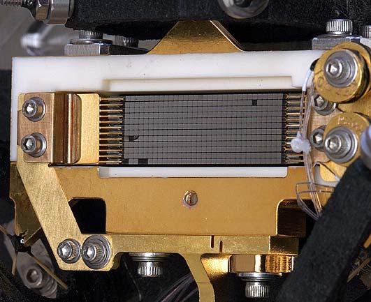
23 SHARC II: 857 GHz (350 microns) 384 elements 1mm pixels Inter-Pixel Correlation ~4% Nyquist Sampled CSO: 10.4 m primary 8.3 FWHM SHARC II Detector Estimated Point Source Response Mars
Astronomy 203 practice final examination
 Astronomy 203 practice final examination Fall 1999 If this were a real, in-class examination, you would be reminded here of the exam rules, which are as follows: You may consult only one page of formulas
The Polarimeter for Observing Inflationary Cosmology at the Reionization Epoch (POINCARE)
") The Polarimeter for Observing Inflationary Cosmology at the Reionization Epoch (POINCARE) D.T. Chuss, J. Hinderks, G. F. Hinshaw, S.H. Moseley, G.M. Voellmer, E.J. Wollack NASA Goddard Space Flight Center,
The Polarimeter for Observing Inflationary Cosmology at the Reionization Epoch (POINCARE) D.T. Chuss, J. Hinderks, G. F. Hinshaw, S.H. Moseley, G.M. Voellmer, E.J. Wollack NASA Goddard Space Flight Center,
HAWC (High Resolution Airborne Wideband Camera) A Facility Camera for SOFIA
 A Facility Camera for SOFIA") HAWC (High Resolution Airborne Wideband Camera) A Facility Camera for SOFIA D.A. Harper (UC) PI Christine Allen (GSFC) Troy Ames (GSFC) Arlin Bartels (GSFC) Sean Casey (USRA) Darren Dowell (Caltech) Rhodri
HAWC (High Resolution Airborne Wideband Camera) A Facility Camera for SOFIA D.A. Harper (UC) PI Christine Allen (GSFC) Troy Ames (GSFC) Arlin Bartels (GSFC) Sean Casey (USRA) Darren Dowell (Caltech) Rhodri
Instrumentation for sub-mm astronomy. Adam Woodcraft SUPA, University of Edinburgh
 Instrumentation for sub-mm astronomy Adam Woodcraft http://woodcraft.lowtemp.org SUPA, University of Edinburgh 1 2 Introduction Sub-mm astronomy 1 Astronomy at sub-mm wavelengths Between infrared and millimetre
Expressions for f r (T ) and Q i (T ) from Mattis-Bardeen theory
 and Q i (T ) from Mattis-Bardeen theory") 8 Appendix A Expressions for f r (T ) and Q i (T ) from Mattis-Bardeen theory The Mattis-Bardeen theory of the anomalous skin effect in superconductors [0] may be used to derive the behavior of the resonance
8 Appendix A Expressions for f r (T ) and Q i (T ) from Mattis-Bardeen theory The Mattis-Bardeen theory of the anomalous skin effect in superconductors [0] may be used to derive the behavior of the resonance
Science Objectives. Test Inflationary models, particle physics at the highest energies
 Cryogenic Detectors for Astrophysics Far-IR, Submillimeter, and CMB Harvey Moseley NASA/GSFC Science Objectives Test Inflationary models, particle physics at the highest energies Inflation Inflation should
Ground and On-Orbit Characterization and Calibration of the Geosynchronous Imaging Fourier Transform Spectrometer (GIFTS)
") Ground and On-Orbit Characterization and Calibration of the Geosynchronous Imaging Fourier Transform Spectrometer (GIFTS) John D. Elwell 1, Deron K. Scott 1 Henry E. Revercomb 2, Fred A. Best 2, Robert
Ground and On-Orbit Characterization and Calibration of the Geosynchronous Imaging Fourier Transform Spectrometer (GIFTS) John D. Elwell 1, Deron K. Scott 1 Henry E. Revercomb 2, Fred A. Best 2, Robert
Thermal noise and correlations in photon detection
 Thermal noise and correlations in photon detection Jonas Zmuidzinas The standard expressions for the noise that is due to photon fluctuations in thermal background radiation typically apply only for a
Large Scale Polarization Explorer
 Science goal and performance (Univ. Roma La Sapienza) for the LSPE collaboration Page 1 LSPE is a balloon payload aimed at: Measure large scale CMB polarization and temperature anisotropies Explore large
HAWC (High Resolution Airborne Wideband Camera) A Facility Camera for SOFIA
 A Facility Camera for SOFIA") HAWC (High Resolution Airborne Wideband Camera) A Facility Camera for SOFIA D.A. Harper (UC) PI Christine Allen (GSFC) Troy Ames (GSFC) Arlin Bartels (GSFC) Sean Casey (USRA) Darren Dowell (Caltech) Rhodri
HAWC (High Resolution Airborne Wideband Camera) A Facility Camera for SOFIA D.A. Harper (UC) PI Christine Allen (GSFC) Troy Ames (GSFC) Arlin Bartels (GSFC) Sean Casey (USRA) Darren Dowell (Caltech) Rhodri
Multiphysics Simulation of Polymer-Based Filters for Sub-Millimetre Space Optics
 Multiphysics Simulation of Polymer-Based Filters for Sub-Millimetre Space Optics N. Baccichet 1, G. Savini 1 1 Department of Physics and Astronomy, University College London, London, UK Sponsored by: EU
1 The formation and analysis of optical waveguides
 1 The formation and analysis of optical waveguides 1.1 Introduction to optical waveguides Optical waveguides are made from material structures that have a core region which has a higher index of refraction
Lasers and Electro-optics
 Lasers and Electro-optics Second Edition CHRISTOPHER C. DAVIS University of Maryland III ^0 CAMBRIDGE UNIVERSITY PRESS Preface to the Second Edition page xv 1 Electromagnetic waves, light, and lasers 1
OPTI510R: Photonics. Khanh Kieu College of Optical Sciences, University of Arizona Meinel building R.626
 OPTI510R: Photonics Khanh Kieu College of Optical Sciences, University of Arizona kkieu@optics.arizona.edu Meinel building R.626 Announcements Homework #6 is assigned, due May 1 st Final exam May 8, 10:30-12:30pm
A TES Bolometer for THz FT-Spectroscopy
 A TES Bolometer for THz FT-Spectroscopy M. Kehrt, J. Beyer, C. Monte, J. Hollandt Physikalisch-Technische Bundesanstalt Abbestraße 2-12, Berlin, Germany E-Mail: Mathias.Kehrt@PTB.de Abstract - We recently
Enhanced performance of microbolometer. using coupled feed horn antenna
 Enhanced performance of microbolometer using coupled feed horn antenna Kuntae Kim*,a, Jong-Yeon Park*, Ho-Kwan Kang*, Jong-oh Park*, Sung Moon*, Jung-ho Park a * Korea Institute of Science and Technology,
Supplementary Figure 1: SAW transducer equivalent circuit
 Supplementary Figure : SAW transducer equivalent circuit Supplementary Figure : Radiation conductance and susceptance of.6um IDT, experiment & calculation Supplementary Figure 3: Calculated z-displacement
point, corresponding to the area it cuts out: θ = (arc length s) / (radius of the circle r) in radians Babylonians:
 / (radius of the circle r) in radians Babylonians:") Astronomische Waarneemtechnieken (Astronomical Observing Techniques) 1 st Lecture: 1 September 11 This lecture: Radiometry Radiative transfer Black body radiation Astronomical magnitudes Preface: The Solid
Astronomische Waarneemtechnieken (Astronomical Observing Techniques) 1 st Lecture: 1 September 11 This lecture: Radiometry Radiative transfer Black body radiation Astronomical magnitudes Preface: The Solid
Introduction to optical waveguide modes
 Chap. Introduction to optical waveguide modes PHILIPPE LALANNE (IOGS nd année) Chapter Introduction to optical waveguide modes The optical waveguide is the fundamental element that interconnects the various
DESIGN OF METALLIC MESH ABSORBERS FOR HIGH BANDWIDTH ELECTROMAGNETIC WAVES
 Progress In Electromagnetics Research C, Vol. 8, 135 147, 2009 DESIGN OF METALLIC MESH ABSORBERS FOR HIGH BANDWIDTH ELECTROMAGNETIC WAVES T. Baron, S. Euphrasie, S. Ben Mbarek, P. Vairac and B. Cretin
Air Force Research Laboratory
 Air Force Research Laboratory Materials with Engineered Dispersion for the Enhancement of Light-Matter Interactions 10 January 2013 Ilya Vitebskiy, AFRL/RYDP Integrity Service Excellence SUBTOPIC 1 Nonreciprocal
Bolometers for submm/mm-wave astronomy
 Bolometers for submm/mm-wave astronomy Wayne S. Holland, William D. Duncan (UK ATC) & Matt Griffin (Cardiff University) Damian Audley (UK ATC) Presented at the 2nd NAIC-NRAO NRAO School on Single-Dish
arxiv: v1 [astro-ph.im] 13 Nov 2015
![arxiv: v1 [astro-ph.im] 13 Nov 2015](/thumbs/87/96678114.jpg "arxiv: v1 [astro-ph.im] 13 Nov 2015") Journal of Low Temperature Physics manuscript No. (will be inserted by the editor) arxiv:1511.04414v1 [astro-ph.im] 13 Nov 2015 D.T. Chuss A. Ali M. Amiri J. Appel C.L. Bennett F. Colazo K.L. Denis R.
Journal of Low Temperature Physics manuscript No. (will be inserted by the editor) arxiv:1511.04414v1 [astro-ph.im] 13 Nov 2015 D.T. Chuss A. Ali M. Amiri J. Appel C.L. Bennett F. Colazo K.L. Denis R.
Fundamental Limits to Wavefront Sensing in the Submillimeter
 Fundamental Limits to Wavefront Sensing in the Submillimeter E. Serabyn Jet Propulsion Laboratory, California Institute of Technology, 4800 Oak Grove Drive, Pasadena, CA, USA 91109 Copyright 2006 Society
MINIMIZING REFLECTION AND FOCUSSING OF INCIDENT WAVE TO ENHANCE ENERGY DEPOSITION IN PHOTODETECTOR S ACTIVE REGION
 Progress In Electromagnetics Research, PIER 65, 71 80, 2006 MINIMIZING REFLECTION AND FOCUSSING OF INCIDENT WAVE TO ENHANCE ENERGY DEPOSITION IN PHOTODETECTOR S ACTIVE REGION A. A. Pavel, P. Kirawanich,
Semiconductor X-Ray Detectors. Tobias Eggert Ketek GmbH
 Semiconductor X-Ray Detectors Tobias Eggert Ketek GmbH Semiconductor X-Ray Detectors Part A Principles of Semiconductor Detectors 1. Basic Principles 2. Typical Applications 3. Planar Technology 4. Read-out
Radio Astronomy An Introduction
 Radio Astronomy An Introduction Felix James Jay Lockman NRAO Green Bank, WV References Thompson, Moran & Swenson Kraus (1966) Christiansen & Hogbom (1969) Condon & Ransom (nrao.edu) Single Dish School
Document Number: SPIRE-UCF-DOC Issue 1.0. November Matt Griffin
 Sensitivity of the SPIRE Detectors to Operating Parameters Document Number: SPIRE-UCF-DOC-9 Issue. November 4 7 Matt Griffin Contents. Introduction.... List of symbols... 3. Principles of semiconductor
Paper Review. Special Topics in Optical Engineering II (15/1) Minkyu Kim. IEEE Journal of Quantum Electronics, Feb 1985
 Minkyu Kim. IEEE Journal of Quantum Electronics, Feb 1985") Paper Review IEEE Journal of Quantum Electronics, Feb 1985 Contents Semiconductor laser review High speed semiconductor laser Parasitic elements limitations Intermodulation products Intensity noise Large
Paper Review IEEE Journal of Quantum Electronics, Feb 1985 Contents Semiconductor laser review High speed semiconductor laser Parasitic elements limitations Intermodulation products Intensity noise Large
Cosmological Studies with SZE-determined Peculiar Velocities. Sarah Church Stanford University
 Cosmological Studies with SZE-determined Peculiar Velocities Sarah Church Stanford University Outline! Why Measure Peculiar Velocities? Cosmological information complements other techniques! Experimental
 Infrared thermography In microwave radiometry hν
 Atacama Submillimeter Telescope. ISM Polarimetry. C. Darren Dowell (JPL/Caltech) 2003 October 11
 2003 October 11") Atacama Submillimeter Telescope ISM Polarimetry C. Darren Dowell (JPL/Caltech) 2003 October 11 Outline Sensitivity Extended Sources: Magnetic fields confront other forces in the Galaxy. Large-scale magnetic
Atacama Submillimeter Telescope ISM Polarimetry C. Darren Dowell (JPL/Caltech) 2003 October 11 Outline Sensitivity Extended Sources: Magnetic fields confront other forces in the Galaxy. Large-scale magnetic
Continuum Observing. Continuum Emission and Single Dishes
 July 11, 2005 NAIC/NRAO Single-dish Summer School Continuum Observing Jim Condon Continuum Emission and Single Dishes Continuum sources produce steady, broadband noise So do receiver noise and drift, atmospheric
Ultra-narrow-band tunable laserline notch filter
 Appl Phys B (2009) 95: 597 601 DOI 10.1007/s00340-009-3447-6 Ultra-narrow-band tunable laserline notch filter C. Moser F. Havermeyer Received: 5 December 2008 / Revised version: 2 February 2009 / Published
Superconductivity Induced Transparency
 Superconductivity Induced Transparency Coskun Kocabas In this paper I will discuss the effect of the superconducting phase transition on the optical properties of the superconductors. Firstly I will give
Modeling of Multi-Layer Anti-Reflective Structuring in a Silicon Lens
 University of Colorado, Boulder CU Scholar Undergraduate Honors Theses Honors Program Fall 2012 Modeling of Multi-Layer Anti-Reflective Structuring in a Silicon Lens Spencer Brugger University of Colorado
Electro-Optical System. Analysis and Design. A Radiometry Perspective. Cornelius J. Willers SPIE PRESS. Bellingham, Washington USA
 Electro-Optical System Analysis and Design A Radiometry Perspective Cornelius J Willers SPIE PRESS Bellingham, Washington USA Nomenclature xvii Preface xxiii 1 Electro-Optical System Design 1 11 Introduction
UNIT I ELECTROSTATIC FIELDS
 UNIT I ELECTROSTATIC FIELDS 1) Define electric potential and potential difference. 2) Name few applications of gauss law in electrostatics. 3) State point form of Ohm s Law. 4) State Divergence Theorem.
Homework Week 3: Nanoscale and macroscale characterization Thermoelectricity: From Atoms to Systems
 Homework Week 3: Nanoscale and macroscale characterization Thermoelectricity: From Atoms to Systems Je-Hyeong Bahk and Ali Shakouri nanohub-u Fall 2013 Answer the thirteen questions including all the sub-questions
Cryogenic thermal mask for space-cold optical testing of space optical systems
 Cryogenic thermal mask for space-cold optical testing of space optical systems Dae Wook Kim ames H. Burge LOFT group College of Optical Sciences Univ. of Arizona Introduction How do the next generation
Supplementary Information Supplementary Figures
 Supplementary Information Supplementary Figures Supplementary Figure S1. Schematic defining the relevant physical parameters in our grating coupler model. The schematic shows a normally-incident light
Lecture 2: Transfer Theory
 Lecture 2: Transfer Theory Why do we study transfer theory? The light we detect arrives at us in two steps: - first, it is created by some radiative process (e.g., blackbody, synchrotron, etc etc ) -
POINCARE. Polarimeter for Observing Inflationary Cosmology at the Reionization Epoch
 POINCARE Polarimeter for Observing Inflationary Cosmology at the Reionization Epoch David T. Chuss NASA Goddard Space Flight Center CMBPol Systematics Workshop Annapolis, MD July 29, 2008 Team Johns Hopkins
Energy transport in metal nanoparticle plasmon waveguides
 Energy transport in metal nanoparticle plasmon waveguides Stefan A. Maier, Pieter G. Kik, and Harry A. Atwater California Institute of Technology Thomas J. Watson Laboratory of Applied Physics, Pasadena,
MoBiKID Kinetic Inductance Detectors for up-coming B-mode satellite experiments
 MoBiKID Kinetic Inductance Detectors for up-coming B-mode satellite experiments TIPP 17 - BEIJING INFN, Sezione di Roma Dawn of the universe: where are we? Looking into the CMB for a proof of the Inflation...
Atmospheric Extinction
 Atmospheric Extinction Calibrating stellar photometry requires correction for loss of light passing through the atmosphere. Atmospheric Rayleigh and aerosol scattering preferentially redirects blue light
Advanced Topic in Astrophysics Lecture 1 Radio Astronomy - Antennas & Imaging
 Advanced Topic in Astrophysics Lecture 1 Radio Astronomy - Antennas & Imaging Course Structure Modules Module 1, lectures 1-6 (Lister Staveley-Smith, Richard Dodson, Maria Rioja) Mon Wed Fri 1pm weeks
A Broadband Flexible Metamaterial Absorber Based on Double Resonance
 Progress In Electromagnetics Research Letters, Vol. 46, 73 78, 2014 A Broadband Flexible Metamaterial Absorber Based on Double Resonance ong-min Lee* Abstract We present a broadband microwave metamaterial
Plasmonic Photovoltaics Harry A. Atwater California Institute of Technology
 Plasmonic Photovoltaics Harry A. Atwater California Institute of Technology Surface plasmon polaritons and localized surface plasmons Plasmon propagation and absorption at metal-semiconductor interfaces
Quasi-Optical Filters
 Quasi-Optical Filters Peter Ade Cardiff School of Physics and Astronomy, Cardiff University, Queens Buildings, The Parade, Cardiff, CF24 3AA Peter.Ade@astro.cf.ac.uk Abstract: We describe the current state-of-art
Chapter 6. Fiber Optic Thermometer. Ho Suk Ryou
 Chapter 6. Fiber Optic Thermometer Ho Suk Ryou Properties of Optical Fiber Optical Fiber Composed of rod core surrounded by sheath Core: conducts electromagnetic wave Sheath: contains wave within the core
Electron-Acoustic Wave in a Plasma
 Electron-Acoustic Wave in a Plasma 0 (uniform ion distribution) For small fluctuations, n ~ e /n 0
International Distinguished Lecturer Program
 U 005-006 International Distinguished Lecturer Program Ken-ya Hashimoto Chiba University Sponsored by The Institute of Electrical and Electronics Engineers (IEEE) Ultrasonics, Ferroelectrics and Frequency
Slide 1. Temperatures Light (Optoelectronics) Magnetic Fields Strain Pressure Displacement and Rotation Acceleration Electronic Sensors
 Magnetic Fields Strain Pressure Displacement and Rotation Acceleration Electronic Sensors") Slide 1 Electronic Sensors Electronic sensors can be designed to detect a variety of quantitative aspects of a given physical system. Such quantities include: Temperatures Light (Optoelectronics) Magnetic
Slide 1 Electronic Sensors Electronic sensors can be designed to detect a variety of quantitative aspects of a given physical system. Such quantities include: Temperatures Light (Optoelectronics) Magnetic
Confocal Microscopy Imaging of Single Emitter Fluorescence and Hanbury Brown and Twiss Photon Antibunching Setup
 1 Confocal Microscopy Imaging of Single Emitter Fluorescence and Hanbury Brown and Twiss Photon Antibunching Setup Abstract Jacob Begis The purpose of this lab was to prove that a source of light can be
Detectors for IR astronomy
 Detectors for IR astronomy Where does infrared begin? Wavelength sensi?vity of the human eye vs. wavelength Note: the eye has some (limited) sensi?vity to IR light at ~1000nm (=0.5x energy of photons the
High-Resolution Gamma-Ray and Neutron Detectors For Nuclear Spectroscopy
 High-Resolution Gamma-Ray and Neutron Detectors For Nuclear Spectroscopy Thomas Niedermayr, I. D. Hau, S. Terracol, T. Miyazaki, S. E. Labov and S. Friedrich Former colleagues: M. F. Cunningham, J. N.
MERIS US Workshop. Instrument Characterization Overview. Steven Delwart
 MERIS US Workshop Instrument Characterization Overview Steven Delwart Presentation Overview On-Ground Characterisation 1. Diffuser characterisation 2. Polarization sensitivity 3. Optical Transmission 4.
Basics of Infrared Detection
 2 Basics of Infrared Detection Before the in-depth analyses of quantum well, ISBT, and QWIP a specific infrared detector we first discuss the general concept of how the temperature of an object influences
An Introduction to Radio Astronomy
 An Introduction to Radio Astronomy Bernard F. Burke Massachusetts Institute of Technology and Francis Graham-Smith Jodrell Bank, University of Manchester CAMBRIDGE UNIVERSITY PRESS Contents Preface Acknowledgements
Nonlinear Effects in Optical Fiber. Dr. Mohammad Faisal Assistant Professor Dept. of EEE, BUET
 Nonlinear Effects in Optical Fiber Dr. Mohammad Faisal Assistant Professor Dept. of EEE, BUET Fiber Nonlinearities The response of any dielectric material to the light becomes nonlinear for intense electromagnetic
Laser Basics. What happens when light (or photon) interact with a matter? Assume photon energy is compatible with energy transition levels.
 interact with a matter? Assume photon energy is compatible with energy transition levels.") What happens when light (or photon) interact with a matter? Assume photon energy is compatible with energy transition levels. Electron energy levels in an hydrogen atom n=5 n=4 - + n=3 n=2 13.6 = [ev]
What happens when light (or photon) interact with a matter? Assume photon energy is compatible with energy transition levels. Electron energy levels in an hydrogen atom n=5 n=4 - + n=3 n=2 13.6 = [ev]
THz direct detector with 2D electron gas periodic structure absorber.
 THz direct detector with D electron gas periodic structure absorber. D. Morozov a, P. Mauskopf a, I. Bacchus a, M. Elliott a, C. Dunscombe a, M. Hopkinson b, M. Henini c a School of Physics and Astronomy,
Chapter 13. Phys 322 Lecture 34. Modern optics
 Chapter 13 Phys 3 Lecture 34 Modern optics Blackbodies and Lasers* Blackbodies Stimulated Emission Gain and Inversion The Laser Four-level System Threshold Some lasers Pump Fast decay Laser Fast decay
Propagation losses in optical fibers
 Chapter Dielectric Waveguides and Optical Fibers 1-Fev-017 Propagation losses in optical fibers Charles Kao, Nobel Laureate (009) Courtesy of the Chinese University of Hong Kong S.O. Kasap, Optoelectronics
Terahertz sensing and imaging based on carbon nanotubes:
 Terahertz sensing and imaging based on carbon nanotubes: Frequency-selective detection and near-field imaging Yukio Kawano RIKEN, JST PRESTO ykawano@riken.jp http://www.riken.jp/lab-www/adv_device/kawano/index.html
Optical Fiber Signal Degradation
 Optical Fiber Signal Degradation Effects Pulse Spreading Dispersion (Distortion) Causes the optical pulses to broaden as they travel along a fiber Overlap between neighboring pulses creates errors Resulting
Advancements in mm-wave On-Wafer Measurements: A Commercial Multi-Line TRL Calibration Author: Leonard Hayden Presenter: Gavin Fisher
 Advancements in mm-wave On-Wafer Measurements: A Commercial Multi-Line TRL Calibration Author: Leonard Hayden Presenter: Gavin Fisher The title of this section is A Commercial Multi-Line TRL Calibration
MUSCAT and Toltec. Dublin KIDs workshop. Dublin 7 th September 2017
 MUSCAT and Toltec Dublin KIDs workshop Dublin 7 th September 2017 Scope of talk Overview of the MUSCAT project and the team Instrument overview System design considerations Detector design consideration
Fabry-Perot Interferometers
 Fabry-Perot Interferometers Astronomy 6525 Literature: C.R. Kitchin, Astrophysical Techniques Born & Wolf, Principles of Optics Theory: 1 Fabry-Perots are best thought of as resonant cavities formed between
Astr 2310 Thurs. March 3, 2016 Today s Topics
 Astr 2310 Thurs. March 3, 2016 Today s Topics Chapter 6: Telescopes and Detectors Optical Telescopes Simple Optics and Image Formation Resolution and Magnification Invisible Astronomy Ground-based Radio
PHYSICS nd TERM Outline Notes (continued)
") PHYSICS 2800 2 nd TERM Outline Notes (continued) Section 6. Optical Properties (see also textbook, chapter 15) This section will be concerned with how electromagnetic radiation (visible light, in particular)
PHYSICS 2800 2 nd TERM Outline Notes (continued) Section 6. Optical Properties (see also textbook, chapter 15) This section will be concerned with how electromagnetic radiation (visible light, in particular)
EE 6313 Homework Assignments
 EE 6313 Homework Assignments 1. Homework I: Chapter 1: 1.2, 1.5, 1.7, 1.10, 1.12 [Lattice constant only] (Due Sept. 1, 2009). 2. Homework II: Chapter 1, 2: 1.17, 2.1 (a, c) (k = π/a at zone edge), 2.3
FINITE-DIFFERENCE FREQUENCY-DOMAIN ANALYSIS OF NOVEL PHOTONIC
 FINITE-DIFFERENCE FREQUENCY-DOMAIN ANALYSIS OF NOVEL PHOTONIC WAVEGUIDES Chin-ping Yu (1) and Hung-chun Chang (2) (1) Graduate Institute of Electro-Optical Engineering, National Taiwan University, Taipei,
ABSTRACT. a Institute for Space Imaging Science, University of Lethbridge, Alberta, T1K 3M4, Canada; b Joint
 The spectral response of the SCUBA-2 850 and 450 micron photometric bands David A. Naylor* a, Brad G. Gom a, Sherif AbdElazim a, Per Friberg b, Daniel Bintley b, Wayne S. Holland c, Michael J. MacIntosh
EPSILON-NEAR-ZERO (ENZ) AND MU-NEAR-ZERO (MNZ) MATERIALS
 AND MU-NEAR-ZERO (MNZ) MATERIALS") EPSILON-NEAR-ZERO (ENZ) AND MU-NEAR-ZERO (MNZ) MATERIALS SARAH NAHAR CHOWDHURY PURDUE UNIVERSITY 1 Basics Design ENZ Materials Lumped circuit elements Basics Decoupling Direction emission Tunneling Basics
EPSILON-NEAR-ZERO (ENZ) AND MU-NEAR-ZERO (MNZ) MATERIALS SARAH NAHAR CHOWDHURY PURDUE UNIVERSITY 1 Basics Design ENZ Materials Lumped circuit elements Basics Decoupling Direction emission Tunneling Basics
Arbitrary Patterning Techniques for Anisotropic Surfaces, and Line Waves
 Arbitrary Patterning Techniques for Anisotropic Surfaces, and Line Waves Dan Sievenpiper, Jiyeon Lee, and Dia a Bisharat January 11, 2016 1 Outline Arbitrary Anisotropic Surface Patterning Surface wave
Effects from the Thin Metallic Substrate Sandwiched in Planar Multilayer Microstrip Lines
 Progress In Electromagnetics Research Symposium 2006, Cambridge, USA, March 26-29 115 Effects from the Thin Metallic Substrate Sandwiched in Planar Multilayer Microstrip Lines L. Zhang and J. M. Song Iowa
Cosmology Large Angular Scale Surveyor. Wednesday, September 25, 13
 Cosmology Large Angular Scale Surveyor T. Marriage for the CLASS Collaboration U. Michigan Cosmology After Planck Sep 24, 2013 CLASS Collaborators NASA GSFC D. Chuss K. Denis A. Kogut N. Miller H. Moseley
Angular-Stability Low-Profile Miniaturized Frequency Selective Surface Based on Complementary Structure
 Progress In Electromagnetics Research M, Vol. 57, 119 128, 2017 Angular-Stability Low-Profile Miniaturized Frequency Selective Surface Based on Complementary Structure Wenxing Li and Yuanyuan Li * Abstract
An Overview of the analysis of two dimensional back illuminated GaAs MESFET
 An Overview of the analysis of two dimensional back illuminated GaAs MESFET Prof. Lochan Jolly*, Ms. Sonia Thalavoor** *(A.P- Department of Electronics & Telecommunication, TCET, Mumbai Email: lochan.jolly@thakureducation.org)
Dr. Tao Li
 Tao Li taoli@nju.edu.cn Nat. Lab. of Solid State Microstructures Department of Materials Science and Engineering Nanjing University Concepts Basic principles Surface Plasmon Metamaterial Summary Light
Supplementary Information
 1 Supplementary Information 3 Supplementary Figures 4 5 6 7 8 9 10 11 Supplementary Figure 1. Absorbing material placed between two dielectric media The incident electromagnetic wave propagates in stratified
Estimation of the Cosmic Microwave Background Radiation
 S.P.Spirydovich Abstract Estimation of the Cosmic Microwave Background Radiation The author discusses some aspects of experiment, which was built to measure temperature of cosmic microwave background (CMB)
Design of Uniform Fiber Bragg grating using Transfer matrix method
 International Journal of Computational Engineering Research Vol, 3 Issue, 5 Design of Uniform Fiber Bragg grating using Transfer matrix method Deba Kumar Mahanta Department of Electrical Engineering, Assam
Chapter 7. Solar Cell
 Chapter 7 Solar Cell 7.0 Introduction Solar cells are useful for both space and terrestrial application. Solar cells furnish the long duration power supply for satellites. It converts sunlight directly
Optimizing the performance of metal-semiconductor-metal photodetectors by embedding nanoparticles in the absorption layer
 Journal of Electrical and Electronic Engineering 2015; 3(2-1): 78-82 Published online February 10, 2015 (http://www.sciencepublishinggroup.com/j/jeee) doi: 10.11648/j.jeee.s.2015030201.27 ISSN: 2329-1613
Physical Basics of Remote-Sensing with Satellites
 - Physical Basics of Remote-Sensing with Satellites Dr. K. Dieter Klaes EUMETSAT Meteorological Division Am Kavalleriesand 31 D-64295 Darmstadt dieter.klaes@eumetsat.int Slide: 1 EUM/MET/VWG/09/0162 MET/DK
Components of a generic collider detector
 Lecture 24 Components of a generic collider detector electrons - ionization + bremsstrahlung photons - pair production in high Z material charged hadrons - ionization + shower of secondary interactions
PHYSICS (PHYS) Physics (PHYS) 1. PHYS 5880 Astrophysics Laboratory
 Physics (PHYS) 1. PHYS 5880 Astrophysics Laboratory") Physics (PHYS) 1 PHYSICS (PHYS) PHYS 5210 Theoretical Mechanics Kinematics and dynamics of particles and rigid bodies. Lagrangian and Hamiltonian equations of motion. PHYS 5230 Classical Electricity And
Physics (PHYS) 1 PHYSICS (PHYS) PHYS 5210 Theoretical Mechanics Kinematics and dynamics of particles and rigid bodies. Lagrangian and Hamiltonian equations of motion. PHYS 5230 Classical Electricity And
1. Consider the biconvex thick lens shown in the figure below, made from transparent material with index n and thickness L.
 Optical Science and Engineering 2013 Advanced Optics Exam Answer all questions. Begin each question on a new blank page. Put your banner ID at the top of each page. Please staple all pages for each individual
linear polarization: the electric field is oriented in a single direction circular polarization: the electric field vector rotates
 Chapter 8 Polarimetry 8.1 Description of polarized radiation The polarization of electromagnetic radiation is described by the orientation of the wave s electric field vector. There are two different cases
4. Integrated Photonics. (or optoelectronics on a flatland)
") 4. Integrated Photonics (or optoelectronics on a flatland) 1 x Benefits of integration in Electronics: Are we experiencing a similar transformation in Photonics? Mach-Zehnder modulator made from Indium
4. Integrated Photonics (or optoelectronics on a flatland) 1 x Benefits of integration in Electronics: Are we experiencing a similar transformation in Photonics? Mach-Zehnder modulator made from Indium
ECE 484 Semiconductor Lasers
 ECE 484 Semiconductor Lasers Dr. Lukas Chrostowski Department of Electrical and Computer Engineering University of British Columbia January, 2013 Module Learning Objectives: Understand the importance of
Demonstration of Near-Infrared Negative-Index Materials
 Demonstration of Near-Infrared Negative-Index Materials Shuang Zhang 1, Wenjun Fan 1, N. C. Panoiu 2, K. J. Malloy 1, R. M. Osgood 2 and S. R. J. Brueck 2 1. Center for High Technology Materials and Department
Temperature Scales and Telescope Efficiencies
 Temperature Scales and Telescope Efficiencies Jeff Mangum (NRAO) April 11, 2006 Contents 1 Introduction 1 2 Definitions 1 2.1 General Terms.................................. 2 2.2 Efficiencies....................................
The Thermal Sieve: a diffractive baffle that provides thermal isolation of a cryogenic optical system from an ambient temperature collimator
 The Thermal Sieve: a diffractive baffle that provides thermal isolation of a cryogenic optical system from an ambient temperature collimator James H. Burge * and Dae Wook Kim College of Optical Sciences
Technique for the electric and magnetic parameter measurement of powdered materials
 Computational Methods and Experimental Measurements XIV 41 Technique for the electric and magnetic parameter measurement of powdered materials R. Kubacki,. Nowosielski & R. Przesmycki Faculty of Electronics,
Laboratory 3: Confocal Microscopy Imaging of Single Emitter Fluorescence and Hanbury Brown, and Twiss Setup for Photon Antibunching
 Laboratory 3: Confocal Microscopy Imaging of Single Emitter Fluorescence and Hanbury Brown, and Twiss Setup for Photon Antibunching Jonathan Papa 1, * 1 Institute of Optics University of Rochester, Rochester,
The Electromagnetic Properties of Materials
 The Electromagnetic Properties of Materials Electrical conduction Metals Semiconductors Insulators (dielectrics) Superconductors Magnetic materials Ferromagnetic materials Others Photonic Materials (optical)