MULTISCALE THERMAL MODELS OF NANOSTRUCTURED DEVICES. Giuseppe Romano
|
|
|
- Frederica Parrish
- 6 years ago
- Views:
Transcription
1 MULTISCALE THERMAL MODELS OF NANOSTRUCTURED DEVICES Giuseppe Romano PhD dissertation XXII CICLO TUTOR: Prof. Aldo Di Carlo COORDINATOR: Prof. Giuseppe Bianchi
2 INTRODUCTION Goodson et al. IEEE Elect. Lett. (2008)


3 INTRODUCTION Quantum DOTs based MESA Muller et al. APL (2006) Carbon nanotube based transistor Infineon
4 OUTLINE Introduction Heat transfer at the nano scale Heat transfer at the meso scale Heat transfer at the macro scale Multiscale model Conclusion
5 Scales Phonon wavelength λ 10nm P D Nanoscale? L P E?
6 Heat balance at the nanoscale Dubi. RMP (2010) The internal energy is stored and dissipated by phonons The vibration is splitted in 3N-6 normal modes (-labeled).
 ]")
7 Heating at the nanoscale VL VR µ L Absorption Emission µ R [ A. Pecchia et al. Report on Progress in Physics (2004) ]
8 Cross sections Phonon-phonon interaction [G. Romano, A. Pecchia and A. Di Carlo J. of Physics: cond. matt. (2007)] P P D E α α = ω Λ N n ) α ( [ E ( N + 1 A N ] = ω ) N Tmol Electron-phonon interaction [A. Pecchia, G. Romano and Aldo Di Carlo Physical Review B (2007)] Transport model Ground state Electron-phonon interaction Non euilibrium Green s Function (NEGF) Density Functional Theory (DFT) Born Approximation (BA)


9 Resonance effect? The absorption can prevail over the emission and cools the molecule [G. Romano, A. Gagliardi, A. Pecchia and Aldo Di Carlo et al. Physical Review B (2010)]


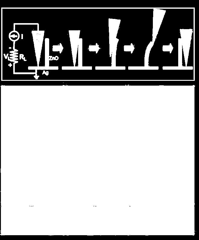
10 Collaboration with experimentalists Thermal instability of fullerenes [G. Schulze, K. Franke, A. Gagliardi, G. Romano, C. Lin, A. Rosa, T. A. Niehaus, T. Frauenheim, A. Di Carlo, A. Pecchia and J. Pascual. Physical Review Letters (2009)]
11 Scales Phonon wavelength λ 10nm Phonon mean free path Λ 100nm Nanoscale Mesoscale P D α Λ α ( N n α )? L P E E ( N + 1) A N?
12 Heat balance at the mesoscale: the gray model Euilibrium energy Thermal flux Temperature 0 e e ~ v ( se ) g = + H τ All phonons are assumed to have the same group velocity (sound velocity) Relaxation time is indipendent of energy phonons. Discontinuous Galerkin Method e T 0 J = = = T 1 4 4π 0 π 4π sv g 4πe + C e dω e dω 0 [Sreekant et al. Heat and Mass Transfer (2006)]
13 Euilibrium energy Since the euilibrium energy depends on the solution itself a self consistent loop is reuired. The first guess of the euilibium energy is a key point for the convergence speed. Usual choice: constant value This work: Fourier simulation 1000 steps 10 steps This approach speeds the convergence up to 100 times
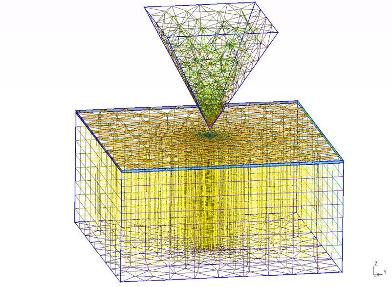
14 GaN uantum dot p-doped Al 0.25 GaN Al 0.25 GaN buffer GaN n-doped Al 0.25 GaN Length = 120 nm
15 GaN uantum dot: meso results Temperature H ~ Current E pz Strain
16 GaN uantum dot: meso results The solid angle is discretized in 18 slices T B M 358K
17 Scales Phonon wavelenght λ 10nm Phonon mean free path Λ 100nm Nanoscale Mesoscale Macroscale P D α Λ α ( N n α ) 4π ( ' s) v g e' dω? L P E E ( N + 1) A N 4π ~ H ( Ω) dω?
 = H H H n p = = J n σ J σ 2 n 2 p p T F M 319K H rec = e( φ φ )R n p")
18 Thermal transport at the macroscales Irreversible thermodynamics Onsager reciprocity relationships Local thermal euilibrium Standard Galerkin Method κ ( T ) = H H H n p = = J n σ J σ 2 n 2 p p T F M 319K H rec = e( φ φ )R n p
19 Scales Phonon wavelenght λ 10nm Phonon mean free path Λ 100nm Nanoscale Mesoscale Macroscale P D α Λ α ( N n α ) 4π ( ' s) v g e' dω κ ( T ) L P E E ( N + 1) A N 4π ~ H ( Ω) dω H

20 THE METHOD Fourier T J m M Gray T Fourier

21 Domain partitioning MACRO DOMAIN MESO DOMAIN MACRO DOMAIN

22 Multiscale model: results Kapitza resistance G. Romano, A. Pecchia and A. Di Carlo. IEEE Journal of Quantum Electronics (in preparation)
23 TiberCAD The models have been implemented in TiberCAD, a multiscale simulator of optoelectronic devices. Input TiberCORE Database Modules Models
24 Conclusion Developed and implemented a model for heating and heat dissipation at the nanoscale (NEGF-DFT) Implemented and optimized a Boltzmann based model for electromodel simulation (Discontinuous Galerkin Method) Implemented the Fourier s law for heat transport (Standard Galerkin Method) Developed and implemented the Macro/Meso multiscale model. Application of the implemented models to several systems, ranging from molecular structures to macro devices.
 4π ( ' s) v g e' dω κ ( T ) L P E E ( N + 1) A N 4π ~ H ( Ω)")
25 Future work Phonon wavelenght λ 10nm Phonon mean free path Λ 100nm Nanoscale Mesoscale Macroscale P D α Λ α ( N n α ) 4π ( ' s) v g e' dω κ ( T ) L P E E ( N + 1) A N 4π ~ H ( Ω) dω H

26 Full integration Mesoscale Nanoscale Macroscale
27 Visiting scholarships 08/ /2009 Georgia Institute of Technology, Atlanta, GA (USA) Supervisor: Prof. Zhong Lin Wang Activities: - FEM simulation of piezoelectric nanogenerators and nanopiezotronic devices. - Investigation on energy harvesting for nanoelectronics - Collaboration with experimentalists. 08/ /2008 Kyoto Institute of Technology, Kyoto (JAPAN). Supervisor: Prof. Giuseppe Pezzotti Activities: - FEM simulation of Raman shift induced by the internal stress. - Investigation on phonon deformation potentials. - Collaboration with experimentalists.
28 DIDACTIC ACTIVITIES GE2008: Nanophotonics and Nanoelectronics: technologies, devices and applications June, Otranto (Italy). International Summer School on Advanced Microelectronics. MIGAS Grenoble (France), Metodi e modelli per la matematica applicata. Prof. Vieri Mastropietro. June-july Dispositivi Elettronici. Prof. Arnaldo D amico, Scuola di Dottorato. Nanoelectronic Modeling: electronic structure and transport at the nanoscale. Prof. Gerhard Klimeck. 5-9 October, 2009
29 PRESENTATIONS G. Romano, G. Mantini, A. Di Carlo, A. D Amico, C. Falconi and Z. L. Wang. Simulation of piezoelectric nanogenerators with TiberCAD. AISEM 2010, Messina (Italy), 8 10, Feb 2010 (Poster). G. Romano, G. Penazzi and A. Di Carlo. Multiscale thermal modeling of GaN/AlGaN uantum DOT LEDs. SPIE Photonics West, San Francisco, CA (USA), 23 28, Jan 2010 (Oral). F. Sacconi, G. Romano, G. Penazzi, M. Povolotskyi, M. Auf der Maur, A. Pecchia and A. Di Carlo. Electronic and transport properties of GaN/ALGaN uantum dot based p-i-n diodes. SISPAD 2008, Hakone (Japan), 9 11, Sep 2008 (Poster). G. Romano, G. Penazzi, M. Auf der Maur, F. Sacconi, M. Povolotskyi, A. Pecchia and A. Di Carlo. TiberCAD: the new multiscale simulator for electronic and optoelectronic devices. 40th Electronic Group Meeting, Otranto (Italy), 16 18, Jun 2008 (Oral). G. Romano, G. Penazzi, M. Auf der Maur, F. Sacconi, M. Povolotskyi, A. Pecchia and A. Di Carlo. A new Multiscale simulator for electronics and optoelectronics devices. New frontiers in micro and nanophotonics, Florence (Italy), 23 26, April 2008 (Oral). G. Romano, M. Auf der Maur, M. Povolotskyi, F. Sacconi, E. Petrolati, A. Pecchia and A. Di Carlo. Multiscale approach in the heat balance problems. International summer school on advanced microelectronics, Grenoble (France), 24 29, Jun 2007 (Poster).
30 PROCEEDINGS G. Romano, G. Penazzi and A. D. Carlo. Multiscale thermal modeling of GaN/AlGaN uantum dot LEDs. Physics and Simulation of Optoelectronic Devices XVIII, 7597(1), 75971S, SPIE (2010). G. Penazzi, A. Pecchia, F. Sacconi, M. Auf der Maur, M. Povolotskyi, G. Romano and A. Di Carlo. Simulations of Optical Properties of a GaN Quantum Dot Embedded in a AlGaN Nanocolumn within a Mixed FEM/atomistic Method. 13th International Workshop on Computational Electronics (IWCE 09), 1 4 (2009). M. Auf der Maur, F. Sacconi, G. Penazzi, M. Povolotskyi, G. Romano, A. Pecchia and A. Di Carlo. Coupling atomistic and finite element approaches for the simulation of optoelectronic devices. 9th International Conference on Numerical Simulation of Optoelectronic Devices (NUSOD), (2009). A. Di Carlo, M. Auf der Maur, F. Sacconi, A. Pecchia, M. Povolotskyi, G. Penazzi and G. Romano. Multiscale atomistic simulations of high-k MOSFETs. Proceedings of the 8 th IEEE International Conference on Nanotechnology (2008). A. Pecchia, G. Romano and A. Di Carlo. Modeling of dissipative transport in molecular systems. Proceedings of the 7th IEEE International Conference on Nanotechnology, (2008). F. Sacconi, G. Romano, G. Penazzi, M. Povolotskyi, M. Auf der Maur, A. Pecchia and A. Di Carlo. Electronic and transport properties of GaN/AlGaN uantum dot-based p-in diodes. (SISPAD 2008), (sept. 2008). M. Auf der Maur, M. Povolotskyi, F. Sacconi, G. Romano, P. E. and A. Di Carlo. Multiscale Simulation of Electronic and Optoelectronic Devices with TiberCAD. SISPAD 2007, (sept. 2007).
31 JOURNAL ARTICLES (1/2) G. Romano, A. Pecchia and A. Di Carlo. Multiscale electro-thermal modeling og GaN/AlGaN uantum dot LEDs. IEEE Journal of uantum electronics, (in preparation). A. Gagliardi, G. Romano, A. Pecchia and A. Di Carlo. Simulation of Inelastic Scattering in Molecular Junctions: Application to Inelastic Electron Tunneling Spectroscopy and Dissipation Effects. Journal of Computational and Theoretical Nanoscience (in press). M. Auf der Maur, F. Sacconi, G. Penazzi, M. Povolotskyi, G. Romano, A. Pecchia and A. Di Carlo. Coupling atomistic and finite element approaches for the simulation of optoelectronic devices. Optical and Quantum Electronics (in press). G. Romano, A. Gagliardi, A. Pecchia and A. Di Carlo. Heating and cooling mechanisms in single-molecule junctions. Physical Review B, 81(11), (2010). A. Gagliardi, G. Romano, A. Pecchia, A. Di Carlo, T. FrauenheElectron-phonon scattering in molecular electronics: From inelastic electron tunnelling spectroscopy to heating effects. im and T. A. Niehaus. New Journal of Physics, 10 (2008). G. Schulze, K. Franke, A. Gagliardi, G. Romano, C. Lin, A. Rosa, T. A. Niehaus, T. Frauenheim, A. Di Carlo, A. Pecchia and J. Pascual. Resonant electron heating and molecular phonon cooling in single C60 junctions. Physical Review Letters, 100(13) (2008).
32 JOURNAL ARTICLES (2/2) A. Pecchia, G. Romano, A. Di Carlo, A. Gagliardi and T. Frauenheim. Joule heating in molecular tunnel junctions: Application to C60. Journal of Computational Electronics, 7(3), (2008). M. Auf Der Maur, M. Povolotskyi, F. Sacconi, A. Pecchia, G. Romano, G. Penazzi and A. Di Carlo. TiberCAD: Towards multiscale simulation of optoelectronic devices. Optical and Quantum Electronics, 40(14-15 SPEC. ISS.), (2008). G. Romano, A. Pecchia and A. Di Carlo. Coupling of molecular vibrons with contact phonon reservoirs. Journal of Physics Condensed Matter, 19(21) (2007). A. Pecchia, G. Romano and A. Di Carlo. Theory of heat dissipation in molecular electronics. Physical Review B, 75(3), (2007). A. Pecchia, G. Romano, A. Gagliardi, T. Frauenheim and A. Di Carlo. Heat dissipation and non-euilibrium phonon distributions in molecular devices. Journal of Computational Electronics, 6(1-3), (2007).


33 Kyoto Institute of Technology, Kyoto (Japan) Aug-Oct 2008 Theoretical piezospectroscopic Deformation potentials Raman shift Prof. Giuseppe Pezzotti


34 Georgia Institute of Technolgy, Atlanta, GA (Aug-Oct 2009) Prof. Zhong Lin Wang
Multiscale-Multiphysics modeling of nanostructured devices: The TiberCAD project.
 Multiscale-Multiphysics modeling of nanostructured devices: The TiberCAD project. M. Auf der Maur, M. Povolotskyi, F. Sacconi, G. Romano, G. Penazzi, A Gagliardi, A. Pecchia, Aldo Di Carlo, Department
The gdftb tool for quantum transport calculations. Alessandro Pecchia CNR - ISMN. University of Roma Tor Vergata
 The gdftb tool for quantum transport calculations Alessandro Pecchia CNR - ISMN Institute for Nanostractured Materials University of Roma Tor Vergata A Gagliardi, G. Romano, G. Penazzi, M. Auf der Maur,
CURRICULUM VITAE OF ALESSANDRO PECCHIA
 CURRICULUM VITAE OF ALESSANDRO PECCHIA Academic Degrees 1/10/1993-10/03/1998 Degree in Physics, Univ. of Trieste (110/110 cum laude). 1/11/1998-30/11/2001 PhD in Leeds, UK (F.W. Carter Prize as Best 2002
Electro-Thermal Transport in Silicon and Carbon Nanotube Devices E. Pop, D. Mann, J. Rowlette, K. Goodson and H. Dai
 Electro-Thermal Transport in Silicon and Carbon Nanotube Devices E. Pop, D. Mann, J. Rowlette, K. Goodson and H. Dai E. Pop, 1,2 D. Mann, 1 J. Rowlette, 2 K. Goodson 2 and H. Dai 1 Dept. of 1 Chemistry
NANO/MICROSCALE HEAT TRANSFER
 NANO/MICROSCALE HEAT TRANSFER Zhuomin M. Zhang Georgia Institute of Technology Atlanta, Georgia New York Chicago San Francisco Lisbon London Madrid Mexico City Milan New Delhi San Juan Seoul Singapore
Nanoscale Energy Transport and Conversion A Parallel Treatment of Electrons, Molecules, Phonons, and Photons
 Nanoscale Energy Transport and Conversion A Parallel Treatment of Electrons, Molecules, Phonons, and Photons Gang Chen Massachusetts Institute of Technology OXFORD UNIVERSITY PRESS 2005 Contents Foreword,
GeSi Quantum Dot Superlattices
 GeSi Quantum Dot Superlattices ECE440 Nanoelectronics Zheng Yang Department of Electrical & Computer Engineering University of Illinois at Chicago Nanostructures & Dimensionality Bulk Quantum Walls Quantum
Daniele Barettin. Classical high school Diploma at Liceo Classico Socrate, Rome, Italy. Maximum grade: 60 / 60
 Daniele Barettin Via Fiume Bianco 47a 00144, Rome Italy + 39-338 - 4114108 (mobile) Daniele.Barettin@uniroma2. it danybaret@gmail.com Italian citizen Date and place of birth: Rome, 11/06/1970 Compulsory
Nanoscale Heat Transfer and Information Technology
 Response to K.E. Goodson Nanoscale Heat Transfer and Information Technology Gang Chen Mechanical Engineering Department Massachusetts Institute of Technology Cambridge, MA 02139 Rohsenow Symposium on Future
Equilibrium Piezoelectric Potential Distribution in a Deformed ZnO Nanowire
 DOI 10.1007/s12274-009-9063-2 Research Article 00624 Equilibrium Piezoelectric Potential Distribution in a Deformed ZnO Nanowire Giulia Mantini 1,2, Yifan Gao 1, A. DʼAmico 2, C. Falconi 2, and Zhong Lin
Progress Report to AOARD
 Progress Report to AOARD C. C. (Chih-Chung) Yang The Graduate Institute of Electro-Optical Engineering National Taiwan University No. 1, Roosevelt Road, Section 4, Taipei, Taiwan (phone) 886-2-23657624
ME 4875/MTE C16. Introduction to Nanomaterials and Nanotechnology. Lecture 2 - Applications of Nanomaterials + Projects
 ME 4875/MTE 575 - C16 Introduction to Nanomaterials and Nanotechnology Lecture 2 - Applications of Nanomaterials + Projects 1 Project Teams of 4 students each Literature review of one application of nanotechnology
CURRICULUM VITAE HUAMIN LI UPDATED: DECEMBER 1, 2015 MAIN RESEARCH INTERESTS EDUCATION
 CURRICULUM VITAE HUAMIN LI UPDATED: DECEMBER 1, 2015 Postdoctoral Research Associate Center for Low Energy Systems Technology (LEAST), Department of Electrical Engineering University of Notre Dame, B20
Intraband emission of GaN quantum dots at λ =1.5 μm via resonant Raman scattering
 Intraband emission of GaN quantum dots at λ =1.5 μm via resonant Raman scattering L. Nevou, F. H. Julien, M. Tchernycheva, J. Mangeney Institut d Electronique Fondamentale, UMR CNRS 8622, University Paris-Sud
Non-equilibrium Green s functions: Rough interfaces in THz quantum cascade lasers
 Non-equilibrium Green s functions: Rough interfaces in THz quantum cascade lasers Tillmann Kubis, Gerhard Klimeck Department of Electrical and Computer Engineering Purdue University, West Lafayette, Indiana
2. TranSIESTA 1. SIESTA. DFT In a Nutshell. Introduction to SIESTA. Boundary Conditions: Open systems. Greens functions and charge density
 1. SIESTA DFT In a Nutshell Introduction to SIESTA Atomic Orbitals Capabilities Resources 2. TranSIESTA Transport in the Nanoscale - motivation Boundary Conditions: Open systems Greens functions and charge
Heat/phonons Transport in Nanostructures and Phononics
 ELTE, Budapest 14 May, 2009 Heat/phonons Transport in Nanostructures and Phononics LI Baowen ( 李保文 ) Centre for Computational Science and Engineering, FOS, & Department of Physics NUS Graduate School for
Nanotechnology, the Technology of Small Thermodynamic Systems 1
 Contents Chapter 1 Nanotechnology, the Technology of Small Thermodynamic Systems 1 1.1 Introduction 1 1.2 Origins of Nanotechnology 1 1.3 What Nanotechnology Is 4 1.3.1 What Can Nanotechnology Do For Us?
Nanomaterials and their Optical Applications
 Nanomaterials and their Optical Applications Winter Semester 2013 Lecture 02 rachel.grange@uni-jena.de http://www.iap.uni-jena.de/multiphoton Lecture 2: outline 2 Introduction to Nanophotonics Theoretical
Achieving a higher performance in bilayer graphene FET Strain Engineering
 SISPAD 2015, September 9-11, 2015, Washington, DC, USA Achieving a higher performance in bilayer graphene FET Strain Engineering Fan W. Chen, Hesameddin Ilatikhameneh, Gerhard Klimeck and Rajib Rahman
Impact Factor Journals of Physics
 Impact Journals of Physics Indexed in ISI Web of Science (JCR SCI, 2016) Compiled By: Arslan Sheikh In Charge Reference & Research Section Library Information Services COMSATS Institute of Information
IH2654 Nanoelectronics, 9hp autumn 2012, period 1 and ****** Nanoelectronics, PhD course
 IH2654 Nanoelectronics, 9hp autumn 2012, period 1 and ****** Nanoelectronics, PhD course For Master programs in Nanotechnology and E, F, ME and PhD students (Previously: 2B1234, 6p and 4H1716, 4p) https://www.kth.se/social/course/ih2654/
3-month progress Report
 3-month progress Report Graphene Devices and Circuits Supervisor Dr. P.A Childs Table of Content Abstract... 1 1. Introduction... 1 1.1 Graphene gold rush... 1 1.2 Properties of graphene... 3 1.3 Semiconductor
Lecture #2 Nanoultrasonic imaging
 Lecture #2 Nanoultrasonic imaging Dr. Ari Salmi www.helsinki.fi/yliopisto 24.1.2014 1 Background Matemaattis-luonnontieteellinen tiedekunta / Henkilön nimi / Esityksen nimi www.helsinki.fi/yliopisto 24.1.2014
Basic Semiconductor Physics
 Chihiro Hamaguchi Basic Semiconductor Physics With 177 Figures and 25 Tables Springer 1. Energy Band Structures of Semiconductors 1 1.1 Free-Electron Model 1 1.2 Bloch Theorem 3 1.3 Nearly Free Electron
Solar Thermoelectric Energy Conversion
 Solar Thermoelectric Energy Conversion Gang Chen Massachusetts Institute of Technology Cambridge, MA 02139 Email: gchen2@mit.edu http://web.mit.edu/nanoengineering NSF Nanoscale Science and Engineering
Graphene Canada Montreal Oct. 16, 2015 (International Year of Light)
") Luminescence Properties of Graphene A. Beltaos 1,2,3, A. Bergren 1, K. Bosnick 1, N. Pekas 1, A. Matković 4, A. Meldrum 2 1 National Institute for Nanotechnology (NINT), 11421 Saskatchewan Drive, Edmonton,
Luminescence Properties of Graphene A. Beltaos 1,2,3, A. Bergren 1, K. Bosnick 1, N. Pekas 1, A. Matković 4, A. Meldrum 2 1 National Institute for Nanotechnology (NINT), 11421 Saskatchewan Drive, Edmonton,
PTES2016 Program for Conference (Venue: Nan Yang Hotel)
") PTES2016 Program for Conference (Venue: Nan Yang Hotel) Thursday, 26 May, 2016 07:30-08:00 Registration 08:00-08:30 Opening Ceremony and Photograph Morning Session I: Thermoelectrics Chair: Prof. Fuli
PTES2016 Program for Conference (Venue: Nan Yang Hotel) Thursday, 26 May, 2016 07:30-08:00 Registration 08:00-08:30 Opening Ceremony and Photograph Morning Session I: Thermoelectrics Chair: Prof. Fuli
How a single defect can affect silicon nano-devices. Ted Thorbeck
 How a single defect can affect silicon nano-devices Ted Thorbeck tedt@nist.gov The Big Idea As MOS-FETs continue to shrink, single atomic scale defects are beginning to affect device performance Gate Source
Device and Monte Carlo Simulation of GaN material and devices. Presenter: Ziyang Xiao Advisor: Prof. Neil Goldsman University of Maryland
 Device and Monte Carlo Simulation of GaN material and devices Presenter: Ziyang Xiao Advisor: Prof. Neil Goldsman University of Maryland 2/23 OUTLINE - GaN Introduction and Background Device Simulation
Acoustic metamaterials in nanoscale
 Acoustic metamaterials in nanoscale Dr. Ari Salmi www.helsinki.fi/yliopisto 12.2.2014 1 Revisit to resonances Matemaattis-luonnontieteellinen tiedekunta / Henkilön nimi / Esityksen nimi www.helsinki.fi/yliopisto
eterostrueture Integrated Thermionic Refrigeration
 eterostrueture Integrated Thermionic Refrigeration Ali Shakouri, and John E. Bowers Department of Electrical and Computer Engineering University of California, Santa Barbara, CA USA 936 ABSTRACT Thermionic
The Physics of Nanoelectronics
 The Physics of Nanoelectronics Transport and Fluctuation Phenomena at Low Temperatures Tero T. Heikkilä Low Temperature Laboratory, Aalto University, Finland OXFORD UNIVERSITY PRESS Contents List of symbols
Introduction to Optoelectronic Device Simulation by Joachim Piprek
 NUSOD 5 Tutorial MA Introduction to Optoelectronic Device Simulation by Joachim Piprek Outline:. Introduction: VCSEL Example. Electron Energy Bands 3. Drift-Diffusion Model 4. Thermal Model 5. Gain/Absorption
Infrared Reflectivity Spectroscopy of Optical Phonons in Short-period AlGaN/GaN Superlattices
 Infrared Reflectivity Spectroscopy of Optical Phonons in Short-period AlGaN/GaN Superlattices J. B. Herzog, A. M. Mintairov, K. Sun, Y. Cao, D. Jena, J. L. Merz. University of Notre Dame, Dept. of Electrical
Spectroscopy at nanometer scale
 Spectroscopy at nanometer scale 1. Physics of the spectroscopies 2. Spectroscopies for the bulk materials 3. Experimental setups for the spectroscopies 4. Physics and Chemistry of nanomaterials Various
Nanophononics. Zlatan Aksamija. Thermal Generation, Transport, and Conversion at the Nanoscale. edited by
 Nanophononics Thermal Generation, Transport, and Conversion at the Nanoscale edited by Nanophononics Nanophononics Thermal Generation, Transport, and Conversion at the Nanoscale edited by Published by
Title: Ultrafast photocurrent measurement of the escape time of electrons and holes from
 Title: Ultrafast photocurrent measurement of the escape time of electrons and holes from carbon nanotube PN junction photodiodes Authors: Nathaniel. M. Gabor 1,*, Zhaohui Zhong 2, Ken Bosnick 3, Paul L.
Semiconductor Physical Electronics
 Semiconductor Physical Electronics Sheng S. Li Department of Electrical Engineering University of Florida Gainesville, Florida Plenum Press New York and London Contents CHAPTER 1. Classification of Solids
GAMINGRE 8/1/ of 7
 FYE 09/30/92 JULY 92 0.00 254,550.00 0.00 0 0 0 0 0 0 0 0 0 254,550.00 0.00 0.00 0.00 0.00 254,550.00 AUG 10,616,710.31 5,299.95 845,656.83 84,565.68 61,084.86 23,480.82 339,734.73 135,893.89 67,946.95
Neutron and x-ray spectroscopy
 Neutron and x-ray spectroscopy B. Keimer Max-Planck-Institute for Solid State Research outline 1. self-contained introduction neutron scattering and spectroscopy x-ray scattering and spectroscopy 2. application
Seminars in Nanosystems - I
 Seminars in Nanosystems - I Winter Semester 2011/2012 Dr. Emanuela Margapoti Emanuela.Margapoti@wsi.tum.de Dr. Gregor Koblmüller Gregor.Koblmueller@wsi.tum.de Seminar Room at ZNN 1 floor Topics of the
Center for Integrated Nanotechnologies (CINT) Bob Hwang Co-Director, Sandia National Laboratories
 Bob Hwang Co-Director, Sandia National Laboratories") Center for Integrated Nanotechnologies (CINT) Bob Hwang Co-Director, Sandia National Laboratories Department of Energy Nanoscience Centers Molecular Foundry Center for Nanoscale Materials Center for Functional
Center for Integrated Nanotechnologies (CINT) Bob Hwang Co-Director, Sandia National Laboratories Department of Energy Nanoscience Centers Molecular Foundry Center for Nanoscale Materials Center for Functional
Импакт-факторы зарубежных научных журналов по физике
 Импакт-факторы зарубежных научных журналов по физике Импактфактор Название журнала п/п 1. REVIEWS OF MODERN 30.254 2. ASTROPHYSICAL JOURNAL SUPPLEMENT SER 14.428 3. MATERIALS SCIENCE & ENGINEERING R-REPORTS
Project Periodic Report
 Project Periodic Report Publishable Summary Grant Agreement n. 256959 Project title Nanoscale energy management for powering ICT devices Project acronym NANOPOWER Call identifier FP7-ICT-2009-5 Funding
Other SPM Techniques. Scanning Probe Microscopy HT10
 Other SPM Techniques Scanning Near-Field Optical Microscopy (SNOM) Scanning Capacitance Microscopy (SCM) Scanning Spreading Resistance Microscopy (SSRM) Multiprobe techniques Electrostatic Force Microscopy,
Self-assembled SiGe single hole transistors
 Self-assembled SiGe single hole transistors G. Katsaros 1, P. Spathis 1, M. Stoffel 2, F. Fournel 3, M. Mongillo 1, V. Bouchiat 4, F. Lefloch 1, A. Rastelli 2, O. G. Schmidt 2 and S. De Franceschi 1 1
Quantum and Non-local Transport Models in Crosslight Device Simulators. Copyright 2008 Crosslight Software Inc.
 Quantum and Non-local Transport Models in Crosslight Device Simulators Copyright 2008 Crosslight Software Inc. 1 Introduction Quantization effects Content Self-consistent charge-potential profile. Space
Supplementary Information: The origin of high thermal conductivity and ultra-low thermal expansion in copper-graphite composites
 Supplementary Information: The origin of high thermal conductivity and ultra-low thermal expansion in copper-graphite composites Izabela Firkowska, André Boden, Benji Boerner, and Stephanie Reich S1 Thermal
Special Topics in Semiconductor Nanotechnology ECE 598XL
 Special Topics in Semiconductor Nanotechnology ECE 598XL Fall 2009 ECE 598XL Syllabus Overview: size matters Formation Process Characterization SOA device applications and potentials Homework or quizzes
Cooling dynamics of glass-embedded metal nanoparticles
 Cooling dynamics of glass-embedded metal nanoparticles Vincent Juvé, Paolo Maioli, Aurélien Crut, Francesco Banfi,, Damiano Nardi, Claudio Giannetti, Stefano Dal Conte, Natalia Del Fatti and Fabrice Vallée
Variation of Electronic State of CUBOID Quantum Dot with Size
 Nano Vision, Vol.1 (1), 25-33 (211) Variation of Electronic State of CUBOID Quantum Dot with Size RAMA SHANKER YADAV and B. S. BHADORIA* Department of Physics, Bundelkhand University, Jhansi-284128 U.P.
GaN-based Devices: Physics and Simulation
 GaN-based Devices: Physics and Simulation Joachim Piprek NUSOD Institute Collaborators Prof. Shuji Nakamura, UCSB Prof. Steve DenBaars, UCSB Dr. Stacia Keller, UCSB Dr. Tom Katona, now at S-ET Inc. Dr.
Spectroscopy at nanometer scale
 Spectroscopy at nanometer scale 1. Physics of the spectroscopies 2. Spectroscopies for the bulk materials 3. Experimental setups for the spectroscopies 4. Physics and Chemistry of nanomaterials Various
GaN and GaN/AlGaN Heterostructure Properties Investigation and Simulations. Ziyang (Christian) Xiao Neil Goldsman University of Maryland
 Xiao Neil Goldsman University of Maryland") GaN and GaN/AlGaN Heterostructure Properties Investigation and Simulations Ziyang (Christian) Xiao Neil Goldsman University of Maryland OUTLINE 1. GaN (bulk) 1.1 Crystal Structure 1.2 Band Structure Calculation
GaN and GaN/AlGaN Heterostructure Properties Investigation and Simulations Ziyang (Christian) Xiao Neil Goldsman University of Maryland OUTLINE 1. GaN (bulk) 1.1 Crystal Structure 1.2 Band Structure Calculation
Spectroscopic Study of FTO/CdSe (MPA)/ZnO Artificial Atoms Emitting White Color
/ZnO Artificial Atoms Emitting White Color") Spectroscopic Study of FTO/CdSe (MPA)/ZnO Artificial Atoms Emitting White Color Batal MA *, and Alyamani K Department of Physics, College of Science, Aleppo, Syria * Corresponding author: Batal MA, Department
Spectroscopic Study of FTO/CdSe (MPA)/ZnO Artificial Atoms Emitting White Color Batal MA *, and Alyamani K Department of Physics, College of Science, Aleppo, Syria * Corresponding author: Batal MA, Department
Lecture 35: Introduction to Quantum Transport in Devices
 ECE-656: Fall 2011 Lecture 35: Introduction to Quantum Transport in Devices Mark Lundstrom Purdue University West Lafayette, IN USA 1 11/21/11 objectives 1) Provide an introduction to the most commonly-used
Contents. Preface to the first edition
 Contents List of authors Preface to the first edition Introduction x xi xiii 1 The nanotechnology revolution 1 1.1 From micro- to nanoelectronics 2 1.2 From the macroscopic to the nanoscopic world 4 1.3
Electrical and Optical Properties. H.Hofmann
 Introduction to Nanomaterials Electrical and Optical Properties H.Hofmann Electrical Properties Ohm: G= σw/l where is the length of the conductor, measured in meters [m], A is the cross-section area of
graphene nano-optoelectronics Frank Koppens ICFO, The institute of photonic sciences, Barcelona
 graphene nano-optoelectronics Frank Koppens ICFO, The institute of photonic sciences, Barcelona Graphene research at ICFO Frank Koppens: group Nano-optoelectronics (~100% graphene) Nano-optics and plasmonics
RAJASTHAN TECHNICAL UNIVERSITY, KOTA
 RAJASTHAN TECHNICAL UNIVERSITY, KOTA (Electronics & Communication) Submitted By: LAKSHIKA SOMANI E&C II yr, IV sem. Session: 2007-08 Department of Electronics & Communication Geetanjali Institute of Technical
Molecular Dynamics Study of Thermal Rectification in Graphene Nanoribbons
 Molecular Dynamics Study of Thermal Rectification in Graphene Nanoribbons Jiuning Hu 1* Xiulin Ruan 2 Yong P. Chen 3# 1School of Electrical and Computer Engineering and Birck Nanotechnology Center, Purdue
Interaction between Single-walled Carbon Nanotubes and Water Molecules
 Workshop on Molecular Thermal Engineering Univ. of Tokyo 2013. 07. 05 Interaction between Single-walled Carbon Nanotubes and Water Molecules Shohei Chiashi Dept. of Mech. Eng., The Univ. of Tokyo, Japan
6.730 Physics for Solid State Applications
 6.730 Physics for Solid State Applications Lecture 29: Electron-phonon Scattering Outline Bloch Electron Scattering Deformation Potential Scattering LCAO Estimation of Deformation Potential Matrix Element
Nanoscience, MCC026 2nd quarter, fall Quantum Transport, Lecture 1/2. Tomas Löfwander Applied Quantum Physics Lab
 Nanoscience, MCC026 2nd quarter, fall 2012 Quantum Transport, Lecture 1/2 Tomas Löfwander Applied Quantum Physics Lab Quantum Transport Nanoscience: Quantum transport: control and making of useful things
Current-Driven Phenomena in NANOELECTRONICS. Edited by Tamar Seideman Northwestern University
 Current-Driven Phenomena in NANOELECTRONICS Edited by Tamar Seideman Northwestern University Published by Pan Stanford Publishing Pte. Ltd. Penthouse Level, Suntec Tower 3 8 Temasek Boulevard Singapore
AKIN AKTURK Carlsbad Drive Gaithersburg, MD 20879, USA
 AKIN AKTURK 1335 Carlsbad Drive Gaithersburg, MD 20879, USA Tel: 240 463 1859 Email: akin.akturk@gmail.com akturka@umd.edu http://www.ece.umd.edu/~akturka EDUCATION Ph. D., Electrical & Computer Engineering,
Olivier Bourgeois Institut Néel
 Olivier Bourgeois Institut Néel Outline Introduction: necessary concepts: phonons in low dimension, characteristic length Part 1: Transport and heat storage via phonons Specific heat and kinetic equation
Report on 7th US-Japan Joint Seminar on Nanoscale Transport Phenomena Science and Engineering
 Report on 7th US-Japan Joint Seminar on Nanoscale Transport Phenomena Science and Engineering December 11-14, 2011, Shima, Japan co-chairs: Shigeo Maruyama, Kazuyoshi Fushinobu, Jennifer Lukes, Li Shi
Nanoelectronics. Topics
 Nanoelectronics Topics Moore s Law Inorganic nanoelectronic devices Resonant tunneling Quantum dots Single electron transistors Motivation for molecular electronics The review article Overview of Nanoelectronic
Thermoelectricity: From Atoms to Systems
 Thermoelectricity: From Atoms to Systems Week 3: Thermoelectric Characterization Lecture 3.6: Summary of Week 3 By Ali Shakouri Professor of Electrical and Computer Engineering Birck Nanotechnology Center
QUANTUM SIMULATION OF NANOCRYSTALLINE COMPOSITE THERMOELECTRIC PROPERTIES
 Proceedings of the ASME 2009 InterPACK Conference IPACK2009 July 19-23, 2009, San Francisco, California, USA Proceedings of ASME/Pacific Rim Technical Conference and Exhibition on Packaging and Integration
Molecular Dynamics Study of Thermal Rectification in Graphene Nanoribbons
 Int J Thermophys (2012) 33:986 991 DOI 10.1007/s10765-012-1216-y Molecular Dynamics Study of Thermal Rectification in Graphene Nanoribbons Jiuning Hu Xiulin Ruan Yong P. Chen Received: 26 June 2009 / Accepted:
5.74 Introductory Quantum Mechanics II
 MIT OpenCourseWare http://ocw.mit.edu 5.74 Introductory Quantum Mechanics II Spring 009 For information about citing these materials or our Terms of Use, visit: http://ocw.mit.edu/terms. Andrei Tokmakoff,
SCORM Based Nano Scale Electronic Devices Modeling Methodology
 Fifth LACCEI International Latin American and Caribbean Conference for Engineering and Technology (LACCEI 2007) Developing Entrepreneurial Engineers for the Sustainable Growth of Latin America and the
Carbon Nanocone: A Promising Thermal Rectifier
 Carbon Nanocone: A Promising Thermal Rectifier Nuo Yang 1, Gang Zhang 2, a) 3,1, b) and Baowen Li 1 Department of Physics and Centre for Computational Science and Engineering, National University of Singapore,
Analysis of flip flop design using nanoelectronic single electron transistor
 Int. J. Nanoelectronics and Materials 10 (2017) 21-28 Analysis of flip flop design using nanoelectronic single electron transistor S.Rajasekaran*, G.Sundari Faculty of Electronics Engineering, Sathyabama
Chapter 3 Properties of Nanostructures
 Chapter 3 Properties of Nanostructures In Chapter 2, the reduction of the extent of a solid in one or more dimensions was shown to lead to a dramatic alteration of the overall behavior of the solids. Generally,
Physics and Material Science of Semiconductor Nanostructures
 Physics and Material Science of Semiconductor Nanostructures PHYS 570P Prof. Oana Malis Email: omalis@purdue.edu Course website: http://www.physics.purdue.edu/academic_programs/courses/phys570p/ 1 Course
 www.iue.tuwien.ac.at/wigner-wiki/ quantum r rmnh h h E a n = a E b n = b h h h n = 1 n = 1 n = 1 0.53 h h n h cos sin 1 1 N ψ = 1 N! ϕ n1 (x 1 ) ϕ n2 (x 1 ) ϕ nn (x 1 ) ϕ n1 (x 2 ) ϕ n2 (x 2
Dottoressa Maria Grazia Carrara. Curriculum Vitae
 Dottoressa Maria Grazia Carrara Personal Data Born in Milan citizen Italian Research grants Curriculum Vitae University of Milano Bicocca via degli Arcimboldi 6 UI-20133 Milano (MI), Italy. +39 02 50317479
MCC026:Nanoscience. at the border between chemistry and physics. Samuel Lara-Avila
 MCC026:Nanoscience at the border between chemistry and physics Samuel Lara-Avila Quantum Device Physics Lab Department of Microtechnology and Nanoscience (MC2) November, 2016 Nanoscience Femto 10-15 Nano:
Büttiker s probe in molecular electronics: Applications to charge and heat transport
 Büttiker s probe in molecular electronics: Applications to charge and heat transport Dvira Segal Department of Chemistry University of Toronto Michael Kilgour (poster) Büttiker s probe in molecular electronics:
chiral m = n Armchair m = 0 or n = 0 Zigzag m n Chiral Three major categories of nanotube structures can be identified based on the values of m and n
 zigzag armchair Three major categories of nanotube structures can be identified based on the values of m and n m = n Armchair m = 0 or n = 0 Zigzag m n Chiral Nature 391, 59, (1998) chiral J. Tersoff,
Nanoscience galore: hybrid and nanoscale photonics
 Nanoscience galore: hybrid and nanoscale photonics Pavlos Lagoudakis SOLAB, 11 June 2013 Hybrid nanophotonics Nanostructures: light harvesting and light emitting devices 2 Hybrid nanophotonics Nanostructures:
SYLLABUS FINDING NANO Syllabus NanoSCI DISCOVERING NANOTECHNOLOGY AND CULTURE IN GERMANY
 1. Syllabus NanoSCI Course title: NanoSCI - Electronic Properties of Nanoengineered Materials Catalog description: Physics and technology of nanoengineered materials and devices. Semiconductor nanostructures.
Carrier Loss Analysis for Ultraviolet Light-Emitting Diodes
 Carrier Loss Analysis for Ultraviolet Light-Emitting Diodes Joachim Piprek, Thomas Katona, Stacia Keller, Steve DenBaars, and Shuji Nakamura Solid State Lighting and Display Center University of California
Computational Study of the Electronic Performance of Cross-Plane Superlattice Peltier Devices
 Purdue University Purdue e-pubs Birck and NCN Publications Birck Nanotechnology Center 3- Computational Study of the Electronic Performance of Cross-Plane Superlattice Peltier Devices Changwook Jeong Network
Understanding Nanoplasmonics. Greg Sun University of Massachusetts Boston
 Understanding Nanoplasmonics Greg Sun University of Massachusetts Boston Nanoplasmonics Space 100pm 1nm 10nm 100nm 1μm 10μm 100μm 1ns 100ps 10ps Photonics 1ps 100fs 10fs 1fs Time Surface Plasmons Surface
Trench IGBT failure mechanisms evolution with temperature and gate resistance under various short-circuit conditions
 Author manuscript, published in "Microelectronics Reliability vol.47 (7) pp.173-1734" Trench IGBT failure mechanisms evolution with temperature and gate resistance under various short-circuit conditions
PHYSICS OF SEMICONDUCTORS AND THEIR HETEROSTRUCTURES
 PHYSICS OF SEMICONDUCTORS AND THEIR HETEROSTRUCTURES Jasprit Singh University of Michigan McGraw-Hill, Inc. New York St. Louis San Francisco Auckland Bogota Caracas Lisbon London Madrid Mexico Milan Montreal
Quantum Mechanical Modeling of Electron-Photon Interactions in Nanoscale Devices
 Progress In Electromagnetics Research, Vol. 154, 163 170, 2015 Quantum Mechanical Modeling of Electron-Photon Interactions in Nanoscale Devices Rulin Wang 1, Yu Zhang 2, Guanhua Chen 2, and Chiyung Yam
Vibrational modes of silicon metalattices from atomistic and finite-element calculations
 Vibrational modes of silicon metalattices from atomistic and finite-element calculations Yihuang Xiong, Weinan hen, Ismaila Dabo Materials Science and Engineering, Penn State University October 6 th, 216
Structure and Dynamics : An Atomic View of Materials
 Structure and Dynamics : An Atomic View of Materials MARTIN T. DOVE Department ofearth Sciences University of Cambridge OXFORD UNIVERSITY PRESS Contents 1 Introduction 1 1.1 Observations 1 1.1.1 Microscopic
Supporting Information
 Electronic Supplementary Material (ESI) for Nanoscale. This journal is The Royal Society of Chemistry 2015 Supporting Information Single Layer Lead Iodide: Computational Exploration of Structural, Electronic
Challenges for Materials to Support Emerging Research Devices
 Challenges for Materials to Support Emerging Research Devices C. Michael Garner*, James Hutchby +, George Bourianoff*, and Victor Zhirnov + *Intel Corporation Santa Clara, CA + Semiconductor Research Corporation
Recap (so far) Low-Dimensional & Boundary Effects
 Low-Dimensional & Boundary Effects") Recap (so far) Ohm s & Fourier s Laws Mobility & Thermal Conductivity Heat Capacity Wiedemann-Franz Relationship Size Effects and Breakdown of Classical Laws 1 Low-Dimensional & Boundary Effects Energy
Recap (so far) Ohm s & Fourier s Laws Mobility & Thermal Conductivity Heat Capacity Wiedemann-Franz Relationship Size Effects and Breakdown of Classical Laws 1 Low-Dimensional & Boundary Effects Energy
Curriculum Vitae M. J. Iqbal Version 14 Sep 2018
 Curriculum Vitae M. J. Iqbal Version 14 Sep 2018 Personal Data Full Name: Muhammad Javaid Iqbal Current Position: Assistant Professor (TTS) Citizenship: i Phone: +92-42-99233133-5 ext. 104 Postal Address:
Curriculum Vitae - Ramoona Shehzadi
 Curriculum Vitae - Ramoona Shehzadi Department of Physics University of the Punjab Lahore, Pakistan Phone: +92-42-99231243 Email: ramoona.physics@pu.edu.pk Personal Date of Birth Marital Status Nationality
Advanced Workshop on Energy Transport in Low-Dimensional Systems: Achievements and Mysteries October 2012
 2371-2 Advanced Workshop on Energy Transport in Low-Dimensional Systems: Achievements and Mysteries 15-24 October 2012 Atomistic Simulations of Thermal Transport in Nanostructured Semiconductors (Thermal