Quantum Informa,on with NV- Centers (QINVC)
|
|
|
- Jayson Blankenship
- 5 years ago
- Views:
Transcription
1 Quantum Informa,on with NV- Centers (QINVC) Jan Meijer (Uni Leipzig) Coopera,on between CEA Saclay France, ENS Cachan France, University StuKgart Germany, University Leipzig Germany, University Warwick United Kingdom


2 Partner 1: CEA- Saclay, Paris D. Esteve group Research Group in Quantum Electronics, CEA- Saclay, France Exper,se: Daniel Esteve (Coordinator) Superconduc,ng quantum circuits Mesoscopic physics Hybrid systems Patrice Bertet


3 Partner 2: ENS Cachan, Paris J.- F. Roch group Exper,se: Quantum op,cs Op,cal and spin proper,es of NV centers AFM with NV- centers Jean- Francois ROCH
 Jörg Wrachtrup")


4 Partner 3: Uni Stutgart (Germany) Jörg Wrachtrup group Exper,se: Spin physics and spin proper,es Direct coupling Inventor of the NV centers as quantum device Jörg Wrachtrup
 J.")


5 Partner 4: University Leipzig (Germany) J. Meijer group Exper,se: Single ion Implanta,on First crea,on of ar,fical NV centers S. Pezzagna J. Meijer S. Pezzagna Small 2010 (Former Prof. Butz group)
")

6 Partner 5: Uni. Warwick (United Kingdom) Mark Newton group Exper,se: Diamond crystal grown (E6) NMR, ESR
7 Material Science Group Solid state quantum Physics P5 Uni Warwick Diamond Growth Characterisa,on P4 Uni Leipzig Addressing of Single NVs P1 CEA Saclay Superconduc,ng Hybrid Circuts P2 ENS Cachan Quantum Op,cs P3(Uni. StuKgart) Spin Physcis Start 2011 ; Dura,on 36 month
 Why NV")
8 Quantum Informa,on with NV- Centers (QINVC) Why NV Centers?


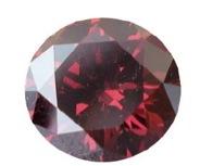
9 Color centers in diamond G- Band: Sp 2 - Inclusion H3- center 3H- Center NV- center Pink star: 62 Mio. Euro J. Rödiger, A. Zaitsev,J. Meijer et. al Unpubl,

10 NV proper,es
 V N V N The main goal to do spin-spin coupling (for the distance < 20 nm with T 2 ~ 1 ms) Lesik et al 2013 G.Balasubramanian et al.")
11 NV Spin proper,es Optically Detected Magnetic Resonance dark state Fluorescence (a. u.) bright state MW frequency (GHz) V N V N The main goal to do spin-spin coupling (for the distance < 20 nm with T 2 ~ 1 ms) Lesik et al 2013 G.Balasubramanian et al., Nature Materials 8, (2009) P.Neumann et al., Nature Physics 6, (2010)
12 NV- centers Easy to ini,alized Long T2,mes, low decoherence Single shot readout Quantum gate opera,on Scalable - > DiVincenzo criteria to build a quantum computer


13 Two Strategies: AFM Quantem Bus hybrid system with superconduc,ng qubits

14 Hybrid Quantum Computer

15 Hybrid System CEA Sacley

16 Single Spin Coupling CEA Sacley

17 AFM Quantum Bus Cachan, UStuK
18 RealizaFon idea: producfon of NV- centers by N implantafon into diamond requirements: technical solufons to implant countable single ions with nm spafal resolufon Physical solu,on: high yield produc,on of NV centers, charge state control, mobility of NV

19 Our aims for NV centres Nanoscalability Nanometer placement Scalability / Reproducibility Shallow centres bulk centres Conversion efficiency Charge state Overall properbes Using Nitrogen ion implantabon
 in diamond N + ions 1 MeV N + ions 5")

20 Ion implantabon - straggling Proton beam (3 MeV) in diamond N + ions 1 MeV N + ions 5 kev 750 nm Low straggling => high resolution Simula,on with SRIM J. Ziegler, hkp://srim.org

21 CreaBon efficiency (N - > NV) Scan of the diamond surface implanted with 1x10 13 nitrogen/cm² 20µm Pezzagna et al., New Journal of Physics 2010, 12,


22 Ion implantabon towards nm resolubon Collimation apertur e Positioning + AFM, STM Resolution of the table ~ 1 nm Meijer et al., Appl. Phys. A 91, 567 (2008)


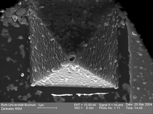
23 Atomic force microscope 50µm Hole made by Focussed Ion Beam Ga + 30keV Tip hole


24 Reduced hole => below 20 nm Non Contact Mode: We can implant into pillars, phtomic crystalls etc. Pezzagna et al., Small. 6, 2117 (2010)
 In")


25 Nitrogen Focused Ion Beam (FIB) In collabora,on with Orsay Physics A wide range of applica,ons Lesik et al., Phys. Stat. Sol. A (2013) Cachan, ULeip
26 High resolubon ion implantabon «Meijer, APL (2005) «Pezzagna, PSSa (2011) «Spinicelli, NJP (2011) «Toyli, NanoLeK (2010) «Lesik, PSSa (2013) «Pezzagna, Small (2010) Pezzagna et al., New J Phys. 13, (2011)
27 RealizaFon idea: producfon of NV- centers by N implantafon into diamond requirements: technical solufons to implant countable single ions with nm spafal resolufon Physical solu,on: high yield produc,on of NV centers, charge state control, mobility of NV

28 Material: E6: 3x3 mm (100) op,cal grade! 100kV CN - Implantaion NV- center H3- center NV 0 NV - 3H- Center ULeip, UStuK J. Rödiger, A. Zaitsev, J. Meijer et. al Unpubl,
29 Crea,on Efficiency UStuK, Warwick
30 Crea,on Efficiency 10x Improvment by anneling op,miza,on

31 No 1100 C 90 min Cachan, ULeip resolu,on 5 nm Wildanger, Roch, Meijer 2012 in prep. Diffusion of single NV? Op,cal detec,on of single NVs:


32 ODMR for orienta,on control Magne,c field Wildanger, Roch, Meijer 2012 in prep.


33 ODMR: Orienta,on of single NVs? No 1100 C 90 min Wildanger, Roch, Meijer 2012 in prep.
34 Charge state control Ac,ve control by applied voltage


35 Individual Adressing Ac,ve control by applied voltage CB 5,47eV 2,0eV 1,2eV NV - NV 0 NV +? Φ E F VB Charge state of NV
36 Bipolar: In- plane PIN- Diode Lohrmann, et al. APL 2011 SP- LED by growing: N. Mizuochi et al. Nature photonics 2012

37 PL- Intensity of a single NV from NV - to NV 0 Lohrmann et al unpubl. May be a dynamic process? beker NV + - > NV -?

38 Addressing of NVs by ac,ve charge control MW Ini,aliza,on

39 Addressing of NVs by ac,ve charge control MW Ini,aliza,on
40 Addressing of NVs by ac,ve charge control Ini,aliza,on
41 Addressing of NVs by ac,ve charge control Ini,aliza,on
42 Conclusion Material science: Op,miza,on in NV produc,on Addressing of NV within 15 nm NVs stable un,l 1300 C No 1100 C First results in coupling NV and superconduc,ng qubits Opimiza,on of the AFM- bus system


43 Thank You! coopera,on with I. Rangelow,Ilmenau and L. Bischop FZR
Towards quantum simulator based on nuclear spins at room temperature
 Towards quantum simulator based on nuclear spins at room temperature B. Naydenov and F. Jelezko C. Müller, Xi Kong, T. Unden, L. McGuinness J.-M. Cai and M.B. Plenio Institute of Theoretical Physics, Uni
Photoelectric readout of electron spin qubits in diamond at room temperature
 Photoelectric readout of electron spin qubits in diamond at room temperature. Bourgeois,, M. Gulka, J. Hruby, M. Nesladek, Institute for Materials Research (IMO), Hasselt University, Belgium IMOMC division,
Coherent manipulation of qubits for quantum hardware : the example of spins in diamond
 GDR CNRS - Nice, 25 mars 2011 Coherent manipulation of qubits for quantum hardware : the example of spins in diamond Jean-François ROCH Lab. de Photonique Quantique et Moléculaire Ecole Normale
Precision sensing using quantum defects
 Precision sensing using quantum defects Sang-Yun Lee 3rd Institute of Physics, University of Stuttgart, Germany Quantum and Nano Control, IMA at University of Minnesota April 14, 2016 Single spin probes
Hybrid Quantum Circuit with a Superconducting Qubit coupled to a Spin Ensemble
 Hybrid Quantum Circuit with a Superconducting Qubit coupled to a Spin Ensemble, Cécile GREZES, Andreas DEWES, Denis VION, Daniel ESTEVE, & Patrice BERTET Quantronics Group, SPEC, CEA- Saclay Collaborating
Maskless and targeted creation of arrays of colour centres in diamond using focused ion beam technology
 Maskless and targeted creation of arrays of colour centres in diamond using focused ion beam technology Margarita Lesik 1,2, Piernicola Spinicelli 1, Sébastien Pezzagna *,1, Patrick Happel 1, Vincent Jacques
Room-Temperature Quantum Sensing in CMOS: On-Chip Detection of Electronic Spin States in Diamond Color Centers for Magnetometry
 Room-Temperature Quantum Sensing in CMOS: On-Chip Detection of Electronic Spin States in Diamond Color Centers for Magnetometry Mohamed I. Ibrahim*, Christopher Foy*, Donggyu Kim*, Dirk R. Englund, and
Magnetic Resonance in Quantum Information
 Magnetic Resonance in Quantum Information Christian Degen Spin Physics and Imaging group Laboratory for Solid State Physics www.spin.ethz.ch Content Features of (nuclear) magnetic resonance Brief History
Implantation of labelled single nitrogen vacancy centers in diamond using 15 N
 Implantation of labelled single nitrogen vacancy centers in diamond using 15 N J. R. Rabeau *, P. Reichart School of Physics, Microanalytical Research Centre, The University of Melbourne, Parkville, Victoria
Quantum manipulation of NV centers in diamond
 Quantum manipulation of NV centers in diamond 12.09.2014 The University of Virginia Physics Colloquium Alex Retzker Jianming Cai, Andreas Albrect, M. B. Plenio,Fedor Jelezko, P. London, R. Fisher,B. Nayedonov,
Nitrogen-Vacancy Centers in Diamond A solid-state defect with applications from nanoscale-mri to quantum computing
 Nitrogen-Vacancy Centers in Diamond A solid-state defect with applications from nanoscale-mri to quantum computing Research into nitrogen-vacancy centers in diamond has exploded in the last decade (see
Shallow Donors in Silicon as Electron and Nuclear Spin Qubits Johan van Tol National High Magnetic Field Lab Florida State University
 Shallow Donors in Silicon as Electron and Nuclear Spin Qubits Johan van Tol National High Magnetic Field Lab Florida State University Overview Electronics The end of Moore s law? Quantum computing Spin
Optical determination and magnetic manipulation of single nitrogen-vacancy color center in diamond nanocrystal
 Optical determination and magnetic manipulation of single nitrogen-vacancy color center in diamond nanocrystal Ngoc Diep Lai, Dingwei Zheng, François Treussart, Jean-François Roch To cite this version:
Lecture 2, March 2, 2017
 Lecture 2, March 2, 2017 Last week: Introduction to topics of lecture Algorithms Physical Systems The development of Quantum Information Science Quantum physics perspective Computer science perspective
Single Photon Generation & Application
 Single Photon Generation & Application Photon Pair Generation: Parametric down conversion is a non-linear process, where a wave impinging on a nonlinear crystal creates two new light beams obeying energy
Quantum Optics. Manipulation of «simple» quantum systems
 Quantum Optics Manipulation of «simple» quantum systems Antoine Browaeys Institut d Optique, Palaiseau, France Quantum optics = interaction atom + quantum field e g ~ 1960: R. Glauber (P. Nobel. 2005),
Quantum control of spin qubits in silicon
 Quantum control of spin qubits in silicon Belita Koiller Instituto de Física Universidade Federal do Rio de Janeiro Brazil II Quantum Information Workshop Paraty, 8-11 September 2009 Motivation B.E.Kane,
Quantum control of proximal spins using nanoscale magnetic resonance imaging
 Quantum control of proximal spins using nanoscale magnetic resonance imaging M. S. Grinolds, P. Maletinsky, S. Hong, M. D. Lukin, R. L. Walsworth and A. Yacoby Nature Physics vol 7 (5) pp.1-6, 2011 DOI:
Silicon-based Quantum Computation. Thomas Schenkel
 Silicon-based Quantum Computation Thomas Schenkel E. O. Lawrence Berkeley National Laboratory T_Schenkel@LBL.gov http://www-ebit.lbl.gov/ Thomas Schenkel, Accelerator and Fusion Research Superconductors
Magnetic Resonance in Quantum
 Magnetic Resonance in Quantum Information Christian Degen Spin Physics and Imaging group Laboratory for Solid State Physics www.spin.ethz.ch Content Features of (nuclear) magnetic resonance Brief History
Quantum Information NV Centers in Diamond General Introduction. Zlatko Minev & Nate Earnest April 2011
 Quantum Information NV Centers in Diamond General Introduction Zlatko Minev & Nate Earnest April 2011 QIP & QM & NVD Outline Interest in Qubits. Why? Quantum Information Motivation Qubit vs Bit Sqrt(Not)
Skyrmions in symmetric bilayers
 Skyrmions in symmetric bilayers A. Hrabec, J. Sampaio, J.Miltat, A.Thiaville, S. Rohart Lab. Physique des Solides, Univ. Paris-Sud, CNRS, 91405 Orsay, France I. Gross, W. Akhtar, V. Jacques Lab. Charles
Driving Qubit Transitions in J-C Hamiltonian
 Qubit Control Driving Qubit Transitions in J-C Hamiltonian Hamiltonian for microwave drive Unitary transform with and Results in dispersive approximation up to 2 nd order in g Drive induces Rabi oscillations
MSN551 LITHOGRAPHY II
 MSN551 Introduction to Micro and Nano Fabrication LITHOGRAPHY II E-Beam, Focused Ion Beam and Soft Lithography Why need electron beam lithography? Smaller features are required By electronics industry:
MIT Department of Nuclear Science & Engineering
 1 MIT Department of Nuclear Science & Engineering Thesis Prospectus for the Bachelor of Science Degree in Nuclear Science and Engineering Nicolas Lopez Development of a Nanoscale Magnetometer Through Utilization
Solid-State Spin Quantum Computers
 Solid-State Spin Quantum Computers 1 NV-Centers in Diamond P Donors in Silicon Kane s Computer (1998) P- doped silicon with metal gates Silicon host crystal + 31 P donor atoms + Addressing gates + J- coupling
Deterministic Coherent Writing and Control of the Dark Exciton Spin using Short Single Optical Pulses
 Deterministic Coherent Writing and Control of the Dark Exciton Spin using Short Single Optical Pulses Ido Schwartz, Dan Cogan, Emma Schmidgall, Liron Gantz, Yaroslav Don and David Gershoni The Physics
Superconducting Qubits Lecture 4
 Superconducting Qubits Lecture 4 Non-Resonant Coupling for Qubit Readout A. Blais, R.-S. Huang, A. Wallraff, S. M. Girvin, and R. J. Schoelkopf, PRA 69, 062320 (2004) Measurement Technique Dispersive Shift
resonances in diamond
 Enhanced dual-beam excitation photoelectric detection of NV magnetic resonances in diamond E. Bourgeois a,b, E. Londero c, K. Buczak d, Y. Balasubramaniam b, G. Wachter d, J. Stursa e, K. Dobes f, F. Aumayr
Electrical Control of Single Spins in Semiconductor Quantum Dots Jason Petta Physics Department, Princeton University
 Electrical Control of Single Spins in Semiconductor Quantum Dots Jason Petta Physics Department, Princeton University g Q 2 m T + S Mirror U 3 U 1 U 2 U 3 Mirror Detector See Hanson et al., Rev. Mod. Phys.
Distributing Quantum Information with Microwave Resonators in Circuit QED
 Distributing Quantum Information with Microwave Resonators in Circuit QED M. Baur, A. Fedorov, L. Steffen (Quantum Computation) J. Fink, A. F. van Loo (Collective Interactions) T. Thiele, S. Hogan (Hybrid
Electron spin qubits in P donors in Silicon
 Electron spin qubits in P donors in Silicon IDEA League lectures on Quantum Information Processing 7 September 2015 Lieven Vandersypen http://vandersypenlab.tudelft.nl Slides with black background courtesy
Inves&ga&on of atomic processes in laser produced plasmas for the short wavelength light sources
 Inves&ga&on of atomic processes in laser produced plasmas for the short wavelength light sources Akira Sasaki Quantum Beam Science Directorate Japan Atomic Energy Agency Introduc&on EUV source at λ=6.5nm
Nuclear spin control in diamond. Lily Childress Bates College
 Nuclear spin control in diamond Lily Childress Bates College nanomri 2010 Hyperfine structure of the NV center: Excited state? Ground state m s = ±1 m s = 0 H = S + gµ S 2 z B z r s r r + S A N I N + S
Let's Build a Quantum Computer!
 Let's Build a Quantum Computer! 31C3 29/12/2014 Andreas Dewes Acknowledgements go to "Quantronics Group", CEA Saclay. R. Lauro, Y. Kubo, F. Ong, A. Palacios-Laloy, V. Schmitt PhD Advisors: Denis Vion,
From nanophysics research labs to cell phones. Dr. András Halbritter Department of Physics associate professor
 From nanophysics research labs to cell phones Dr. András Halbritter Department of Physics associate professor Curriculum Vitae Birth: 1976. High-school graduation: 1994. Master degree: 1999. PhD: 2003.
Nanoscale magnetic imaging with single spins in diamond
 Nanoscale magnetic imaging with single spins in diamond Ania Bleszynski Jayich UC Santa Barbara Physics AFOSR Nanoelectronics Review Oct 24, 2016 Single spin scanning magnetometer Variable temperature
Strain and Temperature Dependence of Defect Formation at AlGaN/GaN High Electron Mobility Transistors on a Nanometer Scale
 Strain and Temperature Dependence of Defect Formation at AlGaN/GaN High Electron Mobility Transistors on a Nanometer Scale Chung-Han Lin Department of Electrical & Computer Engineering, The Ohio State
Lecture 2, March 1, 2018
 Lecture 2, March 1, 2018 Last week: Introduction to topics of lecture Algorithms Physical Systems The development of Quantum Information Science Quantum physics perspective Computer science perspective
Lecture 18 Luminescence Centers
 Lecture 18 Luminescence Centers Read: FS9 (Al2O3 sapphire with different colors) Purdue University Spring 2016 Prof. Yong P. Chen (yongchen@purdue.edu) Lecture 18 (3/24/2016) Slide 1 Basic physics: Vibronic
Quantum Optics in Wavelength Scale Structures
 Quantum Optics in Wavelength Scale Structures SFB Summer School Blaubeuren July 2012 J. G. Rarity University of Bristol john.rarity@bristol.ac.uk Confining light: periodic dielectric structures Photonic
Side resonances and metastable excited state of NV - center in diamond
 Side resonances and metastable excited state of NV - center in diamond Alexander Ivanov 1 and Alexei Ivanov 1 1 Immanuel Kant Baltic Federal University, Nevskogo 14, 236041 Kaliningrad, Russia. aivanov023@gmail.com,
Magnetic Resonance at the quantum limit and beyond
 Magnetic Resonance at the quantum limit and beyond Audrey BIENFAIT, Sebastian PROBST, Xin ZHOU, Denis VION, Daniel ESTEVE, & Patrice BERTET Quantronics Group, SPEC, CEA-Saclay, France Jarryd J. Pla, Cheuk
DISTRIBUTION A: Distribution approved for public release.
 AFRL-AFOSR-CL-TR-2017-0006 Diamond Quantum Nanoemitters 150113 Jeronimo Maze PONTIFICIA UNIVERSIDAD CATOLICA DE CHILE 05/05/2017 Final Report DISTRIBUTION A: Distribution approved for public release. Air
SUPPLEMENTARY INFORMATION
 SUPPLEMENTARY INFORMATION doi: 10.1038/nnano.2011.64 Quantum measurement and orientation tracking of fluorescent nanodiamonds inside living cells L. P. McGuinness, Y. Yan, A. Stacey, D. A. Simpson, L.
SPIN MICROSCOPE BASED ON OPTICALLY DETECTED MAGNETIC RESONANCE
 SPIN MICROSCOPE BASED ON OPTICALLY DETECTED MAGNETIC RESONANCE Boris M. Chernobrod and Gennady P. Berman Theoretical Division, Los Alamos National Laboratory, Los Alamos, NM 87545 Abstract We propose a
Ultra-High-Sensitivity emiccd Cameras Enable Diamond Quantum Dynamics Research
 2015 Princeton Instruments, Inc. All rights reserved. Ultra-High-Sensitivity emiccd Cameras Enable Diamond Quantum Dynamics Research The PI-MAX4:512EM emiccd camera deliver[s] quantitative, ultra-high-sensitivity
tip conducting surface
 PhysicsAndMathsTutor.com 1 1. The diagram shows the tip of a scanning tunnelling microscope (STM) above a conducting surface. The tip is at a potential of 1.0 V relative to the surface. If the tip is sufficiently
Quantum Technologies CCEM Workshop March 23 rd, 2017
 Quantum Technologies CCEM Workshop March 23 rd, 2017 JT Janssen Welcome to the National Physical Laboratory The first quantum revolution h V n f 2 e 1 The second quantum revolution Superposition Entanglement
Confocal Microscope Imaging of Single-Emitter Fluorescence and Photon Antibunching
 Confocal Microscope Imaging of Single-Emitter Fluorescence and Photon Antibunching By Dilyana Mihaylova Abstract The purpose of this lab is to study different types of single emitters including quantum
Study and Manipulation of Photoluminescent NV Color Center in Diamond
 Study and Manipulation of Photoluminescent NV Color Center in Diamond Étude et Manipulation des Propriétés de Spin du Centre Coloré photoluminescent NV dans des nanocristaux de diamant to obtain the title
Commensurability-dependent transport of a Wigner crystal in a nanoconstriction
 NPCQS2012, OIST Commensurability-dependent transport of a Wigner crystal in a nanoconstriction David Rees, RIKEN, Japan Kimitoshi Kono (RIKEN) Paul Leiderer (University of Konstanz) Hiroo Totsuji (Okayama
Quantum technologies based on nitrogen-vacancy centers in diamond: towards applications in (quantum) biology
 biology") Quantum technologies based on nitrogen-vacancy centers in diamond: towards applications in (quantum) biology 3 E 532 nm 1 2δω 1 Δ ESR 0 1 A 1 3 A 2 Microwaves 532 nm polarization Pulse sequence detection
Quantum technologies based on nitrogen-vacancy centers in diamond: towards applications in (quantum) biology 3 E 532 nm 1 2δω 1 Δ ESR 0 1 A 1 3 A 2 Microwaves 532 nm polarization Pulse sequence detection
Single atom doping for quantum device development in diamond and silicon
 Single atom doping for quantum device development in diamond and silicon C. D. Weis and A. Schuh Lawrence Berkeley National Laboratory, 1 Cyclotron Road, Berkeley, California 94114 and Technical University
Imaging Methods: Scanning Force Microscopy (SFM / AFM)
") Imaging Methods: Scanning Force Microscopy (SFM / AFM) The atomic force microscope (AFM) probes the surface of a sample with a sharp tip, a couple of microns long and often less than 100 Å in diameter.
Imaging Methods: Scanning Force Microscopy (SFM / AFM) The atomic force microscope (AFM) probes the surface of a sample with a sharp tip, a couple of microns long and often less than 100 Å in diameter.
2.0 Basic Elements of a Quantum Information Processor. 2.1 Classical information processing The carrier of information
 QSIT09.L03 Page 1 2.0 Basic Elements of a Quantum Information Processor 2.1 Classical information processing 2.1.1 The carrier of information - binary representation of information as bits (Binary digits).
Lecture 2: Double quantum dots
 Lecture 2: Double quantum dots Basics Pauli blockade Spin initialization and readout in double dots Spin relaxation in double quantum dots Quick Review Quantum dot Single spin qubit 1 Qubit states: 450
Quantum error correction on a hybrid spin system. Christoph Fischer, Andrea Rocchetto
 Quantum error correction on a hybrid spin system Christoph Fischer, Andrea Rocchetto Christoph Fischer, Andrea Rocchetto 17/05/14 1 Outline Error correction: why we need it, how it works Experimental realization
Magnetic Resonance with Single Nuclear-Spin Sensitivity. Alex Sushkov
 1 Magnetic Resonance with Single Nuclear-Spin Sensitivity Alex Sushkov 2 MRI scanner $2 million 7 tons 1500 liters of He 3 4 5 µm magnetic force microscopy (MFM) image of hard drive surface topological
MSE 321 Structural Characterization
 Auger Spectroscopy Auger Electron Spectroscopy (AES) Scanning Auger Microscopy (SAM) Incident Electron Ejected Electron Auger Electron Initial State Intermediate State Final State Physical Electronics
CMSC 33001: Novel Computing Architectures and Technologies. Lecture 06: Trapped Ion Quantum Computing. October 8, 2018
 CMSC 33001: Novel Computing Architectures and Technologies Lecturer: Kevin Gui Scribe: Kevin Gui Lecture 06: Trapped Ion Quantum Computing October 8, 2018 1 Introduction Trapped ion is one of the physical
Room temperature entanglement between distant single spins in diamond.
 Room temperature entanglement between distant single spins in diamond. F.Dolde 1, I.Jakobi 1, B.Naydenov 1, 2, N.Zhao 1, S.Pezzagna 3, C.Trautmann 4,5, J.Meijer 3, P.Neumann 1, F.Jelezko 1,2, and J.Wrachtrup
Anisotropic interactions of a single spin and dark-spin spectroscopy in diamond
 Anisotropic interactions of a single spin and dark-spin spectroscopy in diamond R. J. Epstein, F. M. Mendoa, Y. K. Kato & D. D. Awschalom * Center for Spintronics and Quantum Computation, University of
Hyperfine Interaction Estimation of Nitrogen Vacancy Center in Diamond
 Hyperfine Interaction Estimation of Nitrogen Vacancy Center in Diamond Yutaka Shikano Massachusetts Institute of Technology Tokyo Institute of Technology In collaboration with Shu Tanaka (Kinki University,
Impact of Reabsorption on the Emission Spectra and Recombination. Dynamics of Hybrid Perovskite Single Crystals
 Impact of Reabsorption on the Emission Spectra and Recombination Dynamics of Hybrid Perovskite Single Crystals Hiba Diab, 1 Christophe Arnold, 2 Ferdinand Lédée, 1 Gaëlle Trippé-Allard, 1 Géraud Delport,
400 nm Solid State Qubits (1) Daniel Esteve GROUP. SPEC, CEA-Saclay
 Daniel Esteve GROUP. SPEC, CEA-Saclay") 400 nm Solid State Qubits (1) S D Daniel Esteve QUAN UM ELECT RONICS GROUP SPEC, CEA-Saclay From the Copenhagen school (1937) Max Planck front row, L to R : Bohr, Heisenberg, Pauli,Stern, Meitner, Ladenburg,
400 nm Solid State Qubits (1) S D Daniel Esteve QUAN UM ELECT RONICS GROUP SPEC, CEA-Saclay From the Copenhagen school (1937) Max Planck front row, L to R : Bohr, Heisenberg, Pauli,Stern, Meitner, Ladenburg,
Spin electric coupling and coherent quantum control of molecular nanomagnets
 Spin electric coupling and coherent quantum control of molecular nanomagnets Dimitrije Stepanenko Department of Physics University of Basel Institute of Physics, Belgrade February 15. 2010 Collaborators:
Quantum Computation with Neutral Atoms Lectures 14-15
 Quantum Computation with Neutral Atoms Lectures 14-15 15 Marianna Safronova Department of Physics and Astronomy Back to the real world: What do we need to build a quantum computer? Qubits which retain
vapour deposition. Raman peaks of the monolayer sample grown by chemical vapour
 Supplementary Figure 1 Raman spectrum of monolayer MoS 2 grown by chemical vapour deposition. Raman peaks of the monolayer sample grown by chemical vapour deposition (S-CVD) are peak which is at 385 cm
simulations of the Polarization dependence of the light Potential equation in quantum ComPUting
 simulations of the Polarization dependence of the light Potential equation in quantum ComPUting bert david Copsey, student author dr. Katharina gillen, research advisor abstract Many methods of quantum
Lawrence Berkeley National Laboratory Lawrence Berkeley National Laboratory
 Lawrence Berkeley National Laboratory Lawrence Berkeley National Laboratory Title Single ion implantation for solid state quantum computer development Permalink https://escholarship.org/uc/item/0zb737fz
Ultrafast single photon emitting quantum photonic structures. based on a nano-obelisk
 Ultrafast single photon emitting quantum photonic structures based on a nano-obelisk Je-Hyung Kim, Young-Ho Ko, Su-Hyun Gong, Suk-Min Ko, Yong-Hoon Cho Department of Physics, Graduate School of Nanoscience
Quantum computation and quantum information
 Quantum computation and quantum information Chapter 7 - Physical Realizations - Part 2 First: sign up for the lab! do hand-ins and project! Ch. 7 Physical Realizations Deviate from the book 2 lectures,
SUPPLEMENTARY INFORMATION
 doi:10.1038/nature12036 We provide in the following additional experimental data and details on our demonstration of an electrically pumped exciton-polariton laser by supplementing optical and electrical
From trapped ions to macroscopic quantum systems
 7th International Summer School of the SFB/TRR21 "Control of Quantum Correlations in Tailored Matter 21-13 July 2014 From trapped ions to macroscopic quantum systems Peter Rabl Yesterday... Trapped ions:
Mn in GaAs: from a single impurity to ferromagnetic layers
 Mn in GaAs: from a single impurity to ferromagnetic layers Paul Koenraad Department of Applied Physics Eindhoven University of Technology Materials D e v i c e s S y s t e m s COBRA Inter-University Research
Prospects for Superconducting Qubits. David DiVincenzo Varenna Course CLXXXIII
 Prospects for Superconducting ubits David DiVincenzo 26.06.2012 Varenna Course CLXXXIII uantum error correction and the future of solid state qubits David DiVincenzo 26.06.2012 Varenna Course CLXXXIII
Short Course in Quantum Information Lecture 8 Physical Implementations
 Short Course in Quantum Information Lecture 8 Physical Implementations Course Info All materials downloadable @ website http://info.phys.unm.edu/~deutschgroup/deutschclasses.html Syllabus Lecture : Intro
Cavity QED with quantum dots in microcavities
 Cavity QED with quantum dots in microcavities Martin van Exter, Morten Bakker, Thomas Ruytenberg, Wolfgang Löffler, Dirk Bouwmeester (Leiden) Ajit Barve, Larry Coldren (UCSB) Motivation and Applications
Introduction to Nanotechnology Chapter 5 Carbon Nanostructures Lecture 1
 Introduction to Nanotechnology Chapter 5 Carbon Nanostructures Lecture 1 ChiiDong Chen Institute of Physics, Academia Sinica chiidong@phys.sinica.edu.tw 02 27896766 Carbon contains 6 electrons: (1s) 2,
Quantum Information Science (QIS)
") Quantum Information Science (QIS) combination of three different fields: Quantum Physics QIS Computer Science Information Theory Lecture 1 - Outline 1. Quantum Mechanics 2. Computer Science History 3.
Quantum Information Science (QIS) combination of three different fields: Quantum Physics QIS Computer Science Information Theory Lecture 1 - Outline 1. Quantum Mechanics 2. Computer Science History 3.
Universal valence-band picture of. the ferromagnetic semiconductor GaMnAs
 Universal valence-band picture of the ferromagnetic semiconductor GaMnAs Shinobu Ohya *, Kenta Takata, and Masaaki Tanaka Department of Electrical Engineering and Information Systems, The University of
Coherent control of solid state nuclear spin nano-ensembles
 www.nature.com/npjqi ARTICLE OPEN Thomas Unden 1, Nikolas Tomek 1, Timo Weggler 1, Florian Frank 1, Paz London 2, Jonathan Zopes 3, Christian Degen 3, Nicole Raatz 4, Jan Meijer 4, Hideyuki Watanabe 5,
arxiv: v3 [cond-mat.mes-hall] 10 May 2017
![arxiv: v3 [cond-mat.mes-hall] 10 May 2017](/thumbs/71/65757524.jpg "arxiv: v3 [cond-mat.mes-hall] 10 May 2017") Article Nanoscale Sensing Using Point Defects in Single-Crystal Diamond: Recent Progress on Nitrogen Vacancy Center-Based Sensors arxiv:1704.04011v3 [cond-mat.mes-hall] 10 May 2017 Ettore Bernardi, Richard
Article Nanoscale Sensing Using Point Defects in Single-Crystal Diamond: Recent Progress on Nitrogen Vacancy Center-Based Sensors arxiv:1704.04011v3 [cond-mat.mes-hall] 10 May 2017 Ettore Bernardi, Richard
Semiconductor-Detectors
 Semiconductor-Detectors 1 Motivation ~ 195: Discovery that pn-- junctions can be used to detect particles. Semiconductor detectors used for energy measurements ( Germanium) Since ~ 3 years: Semiconductor
Optical Magnetometry Using Nitrogen-Vacancy Centers
 Optical Magnetometry Using Nitrogen-Vacancy Centers Michael Onyszczak Department of Physics and Astronomy, Iowa State University, Ames, IA 50011, U.S.A. Submitted: August 18, 2017 Revised: October 19,
measurement and reduc,on of low- level radon background in the KATRIN experiment Florian M. Fränkle for the KATRIN Collabora9on
 measurement and reduc,on of low- level radon background in the KATRIN experiment Florian M. Fränkle for the KATRIN Collabora9on outline the KATRIN experiment pre-spectrometer background measurement radon
Saroj P. Dash. Chalmers University of Technology. Göteborg, Sweden. Microtechnology and Nanoscience-MC2
 Silicon Spintronics Saroj P. Dash Chalmers University of Technology Microtechnology and Nanoscience-MC2 Göteborg, Sweden Acknowledgement Nth Netherlands University of Technology Sweden Mr. A. Dankert Dr.
Universal enhancement of the optical readout fidelity of single electron spins at nitrogen-vacancy centers in diamond
 Selected for a Viewpoint in Physics PHYSICAL REVIEW B 8, 3525 2 Universal enhancement of the optical readout fidelity of single electron spins at nitrogen-vacancy centers in diamond M. Steiner, P. Neumann,*
Chapter 10: Wave Properties of Particles
 Chapter 10: Wave Properties of Particles Particles such as electrons may demonstrate wave properties under certain conditions. The electron microscope uses these properties to produce magnified images
Quantum physics in quantum dots
 Quantum physics in quantum dots Klaus Ensslin Solid State Physics Zürich AFM nanolithography Multi-terminal tunneling Rings and dots Time-resolved charge detection Moore s Law Transistors per chip 10 9
Opto-electronic Characterization of Perovskite Thin Films & Solar Cells
 Opto-electronic Characterization of Perovskite Thin Films & Solar Cells Arman Mahboubi Soufiani Supervisors: Prof. Martin Green Prof. Gavin Conibeer Dr. Anita Ho-Baillie Dr. Murad Tayebjee 22 nd June 2017
Квантовые цепи и кубиты
 Квантовые цепи и кубиты Твердотельные наноструктуры и устройства для квантовых вычислений Лекция 2 А.В. Устинов Karlsruhe Institute of Technology, Germany Russian Quantum Center, Russia Trapped ions Degree
The nitrogen-vacancy colour centre in diamond
 The nitrogen-vacancy colour centre in diamond arxiv:1302.3288v1 [cond-mat.mtrl-sci] 14 Feb 2013 Marcus W. Doherty, a,b Neil B. Manson, b Paul Delaney, c Fedor Jelezko, d Jörg Wrachtrup e and Lloyd C.L.
Optical Investigation of the Localization Effect in the Quantum Well Structures
 Department of Physics Shahrood University of Technology Optical Investigation of the Localization Effect in the Quantum Well Structures Hamid Haratizadeh hamid.haratizadeh@gmail.com IPM, SCHOOL OF PHYSICS,
Quantum Condensed Matter Physics Lecture 12
 Quantum Condensed Matter Physics Lecture 12 David Ritchie QCMP Lent/Easter 2016 http://www.sp.phy.cam.ac.uk/drp2/home 12.1 QCMP Course Contents 1. Classical models for electrons in solids 2. Sommerfeld
Solid State Device Fundamentals
 Solid State Device Fundamentals ENS 345 Lecture Course by Alexander M. Zaitsev alexander.zaitsev@csi.cuny.edu Tel: 718 982 2812 Office 4N101b 1 Outline - Goals of the course. What is electronic device?
SUPPLEMENTARY INFORMATION
 Quantitative nanoscale vortex imaging using a cryogenic quantum magnetometer L. Thiel, D. Rohner, M. Ganzhorn, P.Appel, E. Neu, B. Müller, R. Kleiner, D. Koelle, and P. Maletinsky (Dated: March 7, 2016)
Nanoscience galore: hybrid and nanoscale photonics
 Nanoscience galore: hybrid and nanoscale photonics Pavlos Lagoudakis SOLAB, 11 June 2013 Hybrid nanophotonics Nanostructures: light harvesting and light emitting devices 2 Hybrid nanophotonics Nanostructures:
Physics and Material Science of Semiconductor Nanostructures
 Physics and Material Science of Semiconductor Nanostructures PHYS 570P Prof. Oana Malis Email: omalis@purdue.edu Course website: http://www.physics.purdue.edu/academic_programs/courses/phys570p/ 1 Course