Radiation Hardness Study on Double Sided 3D Sensors after Proton and Neutron Irradiation up to HL-LHC Fluencies
|
|
|
- Caren Hines
- 5 years ago
- Views:
Transcription
1 Radiation Hardness Study on Double Sided 3D Sensors after Proton and Neutron Irradiation up to HL-LHC Fluencies D M S Sultan 1, G.-F. Dalla Betta 1, R. Mendicino 1, M. Boscardin 2 1 University of Trento and INFN, Italy 2 Fondazione Bruno Kessler (FBK), Italy INFN Laboratori Nazionali di Legnaro (Padova)
2 OUTLINE Introduction & Motivation Results from the electrical characterizations: Passing-Through Columns (IBL technology) Modified Non-Passing-Through Columns Comparative Investigations Conclusion
 328 C. Kenney et. al.")
 - Fast response times - smaller trapping probability after irradiation High radiation hardness Cell Shielding Effect Active Edge and")
3 p D M S SULTAN S. Parker et. al. NIMA 395 (1997) 328 C. Kenney et. al. IEEE TNS 48(6) (2001) 2405 n n Introduction p 3D Radiation Sensors ADVANTAGES: Electrode distance and active substrate thickness decoupled: - Low depletion voltage (~10 V, before irradiation) - Fast response times - smaller trapping probability after irradiation High radiation hardness Cell Shielding Effect Active Edge and Slim-Edge Technology Sensitivity up to few µm from the edge DISADVANTAGES: Non uniform spatial response Higher capacitance with respect to planar Complicated technology (wafer bonding, DRIE, etc.) support wafer oxide C. Kenney et. al. IEEE TNS 46(4) (1999) 1224
 (2008), 2775 G. Pellegrini et. Al.")
 Back-side accessible Easier assembly")
4 Double-sided 3D sensors FBK (Trento, Italy) CNM (Barcelona, Spain) A. Zoboli et. al., IEEE TNS 55(5) (2008), 2775 G. Pellegrini et. Al. NIMA 592(2008), 38 Support wafer is not used reduced process complexity First Joint Production of 3D pixels accomplished for ATLAS IBL (FBK & CNM) Back-side accessible Easier assembly within a detector system Active edge not feasible Slim edge

 (2013) 2357")

5 FBK 3D Pixels for ATLAS IBL Electrical tests FEI4 G. Giacomini, et al., IEEE TNS 60(3) (2013) 2357 p-irrad, 5e15 n eq cm -2 The ATLAS IBL Collaboration, JINST 7 (2012) P11010
6 Charge collection in FE-I4 pixels with 90 Sr beta source S. Grinstein, Sh. Tsiskaridze, A. Micelli, C. Gemme

 For further improvements, it is important to learn more about breakdown behavior")
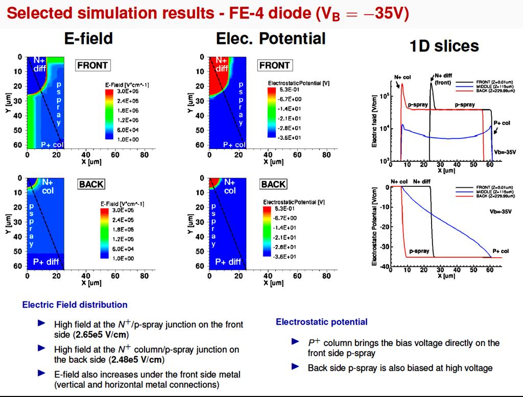
7 Breakdown voltage in FBK sensors In FBK 3D sensors the intrinsic breakdown occurs at the n + /p-spray junctions G. Giacomini et. al., IEEE TNS 60(3) (2013) 2357 P-spray doping reduction improved V bd from ~20 V (ATLAS08) to >60 V (IBL production, A09-II) For further improvements, it is important to learn more about breakdown behavior High P-Spray Lower Low P-Spray P-Spray Most critical regions for breakdown
 22 26 Comparable electric field peaks on front side and back side for std.")
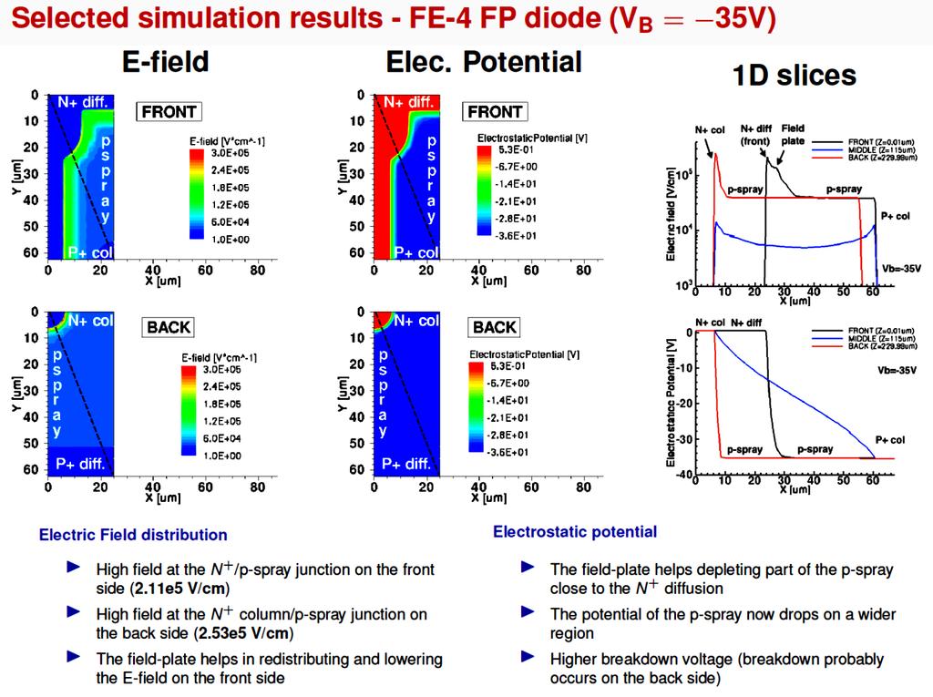
8 Field-Plate Effect on Electric field 35V w/o FP w FP M. Povoli et al, NIMA 699 (2013) Comparable electric field peaks on front side and back side for std. structures The field-plate helps in redistributing and lowering the E-field on the front side (breakdown on the back side )


9 Improved design Most critical zone for VV bd removed Intrinsic Breakdown Increases up to 70 V V M. Povoli et al, NIMA 699 (2013) Dalla Betta et al, (NSS/MIC), 2013 IEEE
10 Since breakdown voltage improves with ionizing dose (higher oxide charge), the same improvement should be observed after irradiation Is it also better after irradiation? Dedicated irradiation tests were performed to check this point a) 800 MeV protons at LANSCE facility Thanks to Martin Hoeferkamp and Sally Seidel b) TRIGA reactor neutrons at JSI Ljubljana, Slovenia Thanks to Vladimir Cindro


11 Layout Diversity µm 56.6 µm Field Plate 67.3 µm Considered Simulation zone Different shapes, sizes and column configurations Different distances between n+ and p+ regions With and without field-plate (Passing Through Col. 3D Si Sensors) & Only with field plate (Non Passing Through Col. 3D Si Sensors)
12 IBL 3D Passing-Through Sensor with Proton Irrad. DATA: R. Mendicino et al, V bbbb has shown to be dependent of Layout Diversity, Field-plate inclusion and Irrad. fluencies. Field-plate improves to have Greater Breakdown Voltage. High fluencies evidently improves the breakdown voltage Field-plate has maintained on all Modified IBL process and next generation

13 IBL 3D Passing-Through Sensor with Proton Irrad. Measured at 1KHz Depletion Voltage increases around 100 V for proton irradiation fluencies up to 2x10 15 nn eeee /cccc 2
14 IBL 3D Passing-Through Sensor with Neutron Irrad. DATA: R. Mendicino et al, Breakdown voltage dependance upon different neutron irrad. fluencies has addressed Leakage current increases with higher fluencies Smooth increase of breakdown voltage shows quite good agreement with expectation (low gamma ray background Lower Surface Damage) Lower breakdown achieved here in comparison to the effect from Proton irrad. anticipates the contribution from bulk damage mostly!
15 IBL 3D Passing-Through Sensor with Neutron Irrad. Measured at 1KHz Depletion voltage increases with higher irradiation fluences At high fluencies, full depletion voltage can not be achieved due to breakdown 5e 1111 Good agreement with expectation!!
16 Current (µa) 5 D M S SULTAN 3D Non Passing-Through Sensor with Proton I-V of Different Proton Irrad. Fluencies [-10 o C] 15 Breakdown Voltage, VV FEI4 LANCSE 7.3e 15 bbbb, increased upto 260V for FEI4 & 290V for CMS at higher FEI4 LANCSE 4e 15 irrad. Dose FEI4 LANCSE 6.9e 14 For CMS, VV bbbb has seen ~290 V just for 10 CMS LANCSE 4e 15 nominal 4ee 15 nn eeee /cccc 2 CMS LANCSE 6.9e 14 At VV bbbb,sharp increase in the current points to probable n-col. tip-effect 4e Voltage (V) SHR Agrreement up to large voltages near to VV bbbb both CMS & FEI4 Activation Energy has considered 1.21 ev.
17 3D Non Passing-Through Sensor with Proton Measured at 1KHz Measured at 1KHz 6.9e14 4e15 7.3e15 Full depletion voltage shifts at higher voltage with the appliance of higher irrad. Dose. For the fluence, 5ee 15 nn eeee /cccc 2, it is evedent that Full depletion voltage shifts to >~100V Bias Operation range becomes limited at higher fluencies At more LH-HLC fluence, this effect would appear more adversely.
18 3D Non Passing-Through Sensor with Neutron Irrad. Breakdown Voltage, VV bbbb, reaches up to 200 V at higher neutron Irradiation nn eeee /cccc 2 Neutron irrad. VV bbbb is lower than Proton irrad. Still the sharp breakdown appeared. Arrhenius plot has shown quite good agreement with SRH theory up to large voltage

19 3D Non Passing-Through Sensor with Neutron As expected, full depletion voltage appears at very near to Breakdown Voltage, VV bbbb. Surface damage is comparatively Smaller in Neutron Irrad. than Proton Irrad V V Increment of irrad. dose increases the full depletion voltage Significantly, limiting bias operating range!
20 Voltage(V) D M S SULTAN Passing Through with Proton Irrad. FEI4 Breakdown FEI4 Depletion CMS Breakdown CMS Depletion ~50 V (Approx. operating bias voltage range) Depletion Voltage Comparative Investigations Breakdown Voltage Fluence x Passing Through with Neutron Irrad. Voltage(V) Non Passing Through with Proton Irrad. ~135 V (Approx. operating bias voltage range) Breakdown Voltage ~80 V (Approx. operating bias voltage range) 100 FEI4 Breakdown 50 Depletion FEI4 Depletion Voltage CMS Breakdown CMS Depletion Fluence x Non passing Passing Through with Neutron Irrad. 300 Voltage(V) Fully depletion voltage appears almost at V bbbb FEI4 Breakdown FEI4 Depletion Fluence x Voltage(V) FEI4 Breakdown FEI4 Depletion Breakdown Voltage ~19 V (Approx. operating bias voltage range) Depletion Voltage Fluence x 10 15
21 Conclusion The extended electrical characterization of IBL and modified 3D-DDTC sensors of FBK 4-inch tech. has been shown up to large fluencies The critical analysis of IBL 3D batches limitation regarding V bd has been addressed Ongoing limitation of Modified IBL 3D batches has pointed to n-column tip effect Modified technology showed promising candidate for complying the radiation hardness of foreseen HL-LHC Charge collection efficiency within new non-passing through technology yet to be investigated.
22 Thank You for Paying Your Attention!
23 Backup Slides
24 Marco Povoli et al, Impact Ionization effect Pre-Irrad. Condition) on leakage current was widely seen on Passing Through Col. 3D Sensors at lower temperature
25 Jiaguo Zhang, PhD Thesis, University of Hamburg, 2013
26
27

28
AIDA-2020 Advanced European Infrastructures for Detectors at Accelerators. Conference/Workshop Paper
 AIDA-2020-CONF-2016-007 AIDA-2020 Advanced European Infrastructures for Detectors at Accelerators Conference/Workshop Paper Measurements and TCAD Simulations of Bulk and Surface Radiation Damage Effects
RD50 Recent Results - Development of radiation hard sensors for SLHC
 - Development of radiation hard sensors for SLHC Anna Macchiolo Max-Planck-Institut für Physik Föhringer Ring 6, Munich, Germany E-mail: Anna.Macchiolo@mppmu.mpg.de on behalf of the RD50 Collaboration
Simulation results from double-sided and standard 3D detectors
 Simulation results from double-sided and standard 3D detectors David Pennicard, University of Glasgow Celeste Fleta, Chris Parkes, Richard Bates University of Glasgow G. Pellegrini, M. Lozano - CNM, Barcelona
Radiation hardness of Low Gain Amplification Detectors (LGAD)
") Radiation hardness of Low Gain Amplification Detectors (LGAD) G. Kramberger, V. Cindro, I. Mandić, M. Mikuž Ϯ, M. Zavrtanik Jožef Stefan Institute, Ljubljana, Slovenia Ϯ also University of Ljubljana, Faculty
Radiation hardness of Low Gain Amplification Detectors (LGAD) G. Kramberger, V. Cindro, I. Mandić, M. Mikuž Ϯ, M. Zavrtanik Jožef Stefan Institute, Ljubljana, Slovenia Ϯ also University of Ljubljana, Faculty
Mara Bruzzi INFN and University of Florence, Italy and SCIPP, UC Santa Cruz, USA
 SCIPP 06/16 September 2006 Capacitance-Voltage analysis at different temperatures in heavily irradiated silicon detectors Mara Bruzzi INFN and University of Florence, Italy and SCIPP, UC Santa Cruz, USA
Charge Collection and Capacitance-Voltage analysis in irradiated n-type magnetic Czochralski silicon detectors
 Charge Collection and Capacitance-Voltage analysis in irradiated n-type magnetic Czochralski silicon detectors M. K. Petterson, H.F.-W. Sadrozinski, C. Betancourt SCIPP UC Santa Cruz, 1156 High Street,
Ranjeet Dalal, Ashutosh Bhardwaj, Kirti Ranjan, Kavita Lalwani and Geetika Jain
 Simulation of Irradiated Si Detectors, Ashutosh Bhardwaj, Kirti Ranjan, Kavita Lalwani and Geetika Jain CDRST, Department of physics and Astrophysics, University of Delhi, India E-mail: rdalal@cern.ch
Silicon Detectors for the slhc an Overview of Recent RD50 Results
 Silicon Detectors for the slhc an Overview of Recent Results Institut für Experimentelle Kernphysik on behalf of the Collaboration 1 Overview Radiation environment and requirements for silicon sensors
Combined Bulk and Surface Radiation Damage Effects at Very High Fluences in Silicon Detectors: Measurements and TCAD Simulations
 Combined Bulk and Surface Radiation Damage Effects at Very High Fluences in Silicon Detectors: Measurements and TCAD Simulations F. Moscatelli, D. Passeri, Member, IEEE, A. Morozzi, Student Member, IEEE,
World irradiation facilities for silicon detectors
 World irradiation facilities for silicon detectors Vladimir Cindro Jožef Stefan Institute Jamova 39, 1000 Ljubljana, Slovenia E-mail: vladimir.cindro@ijs.si Several irradiation facilities are used for
Design, Simulation, Fabrication, and Preliminary Tests of 3D CMS Pixel Detectors for the Super-LHC
 Physics Physics Research Publications Purdue University Year 2010 Design, Simulation, Fabrication, and Preliminary Tests of 3D CMS Pixel Detectors for the Super-LHC O. Koybasi, D. Bortoletto, T. E. Hansen,
X-ray induced radiation damage in segmented p + n silicon sensors
 in segmented p + n silicon sensors Jiaguo Zhang, Eckhart Fretwurst, Robert Klanner, Joern Schwandt Hamburg University, Germany E-mail: jiaguo.zhang@desy.de Deutsches Elektronen-Synchrotron (DESY), Germany
Development of Radiation Hard Si Detectors
 Development of Radiation Hard Si Detectors Dr. Ajay K. Srivastava On behalf of Detector Laboratory of the Institute for Experimental Physics University of Hamburg, D-22761, Germany. Ajay K. Srivastava
Development of a Radiation Hard CMOS Monolithic Pixel Sensor
 Development of a Radiation Hard CMOS Monolithic Pixel Sensor M. Battaglia 1,2, D. Bisello 3, D. Contarato 2, P. Denes 2, D. Doering 2, P. Giubilato 2,3, T.S. Kim 2, Z. Lee 2, S. Mattiazzo 3, V. Radmilovic
Aspects of radiation hardness for silicon microstrip detectors
 Aspects of radiation hardness for silicon microstrip detectors Richard Wheadon, INFN Pisa, Via Livornese 1291, S. Piero a Grado, Pisa, Italy Abstract The ways in which radiation damage affects the properties
Characterization of Irradiated Doping Profiles. Wolfgang Treberspurg, Thomas Bergauer, Marko Dragicevic, Manfred Krammer, Manfred Valentan
 Characterization of Irradiated Doping Profiles, Thomas Bergauer, Marko Dragicevic, Manfred Krammer, Manfred Valentan Vienna Conference on Instrumentation (VCI) 14.02.2013 14.02.2013 2 Content: Experimental
Tracking Detector Material Issues for the slhc
 Tracking Detector Material Issues for the slhc Hartmut F.-W. Sadrozinski SCIPP, UC Santa Cruz, CA 95064 Hartmut F.-W. Sadrozinski, US ATLAS Upgrade Meeting Nov 10, 2005 1 Outline of the talk - Motivation
3D Sensor Measurements at Univ. New Mexico
 3D Sensor Measurements at Univ. New Mexico Martin Hoeferkamp 10 Nov 2005 Introduction Framework: to assist ATLAS in selecting a technology for pixel sensors in the upgrade era. Specifically: to evaluate
SURVEY OF RECENT RADIATION DAMGE STUDIES AT HAMBURG
 SURVEY OF RECENT RADIATION DAMGE STUDIES AT HAMBURG E. Fretwurst 1, D. Contarato 1, F. Hönniger 1, G. Kramberger 2 G. Lindström 1, I. Pintilie 1,3, A. Schramm 1, J. Stahl 1 1 Institute for Experimental
Preliminary measurements of charge collection and DLTS analysis of p + /n junction SiC detectors and simulations of Schottky diodes
 Preliminary measurements of charge collection and DLTS analysis of p + /n junction SiC detectors and simulations of Schottky diodes F.Moscatelli, A.Scorzoni, A.Poggi, R.Nipoti DIEI and INFN Perugia and
Radiation Damage in Silicon Particle Detectors in High Luminosity Experiments
 Radiation Damage in Silicon Particle Detectors in High Luminosity Experiments Agnieszka Obłąkowska-Mucha AGH UST Kraków within the framework of RD50 Collaboration & LHCb VELO Group 2nd Jagiellonian Symposium
Semiconductor materials and detectors for future very high luminosity colliders
 Semiconductor materials and detectors for future very high luminosity colliders Andrea Candelori Istituto Nazionale di Fisica Nucleare (INFN), Italy On behalf of the CERN Collaboration (http://rd5.web.cern.ch/rd5/)
Radiation Effects nm Si 3 N 4
 The Active DEPFET Pixel Sensor: Irradiation Effects due to Ionizing Radiation o Motivation / Radiation Effects o Devices and Facilities o Results o Summary and Conclusion MPI Semiconductor Laboratory Munich
Energy calibration of the threshold of Medipix for ATLAS
 Energy calibration of the threshold of Medipix for ATLAS Céline Lebel Université de Montréal lebel@lps.umontreal.ca presenting for the Institut of Experimental and Applied Physics of the Czech Technical
PoS(VERTEX2015)027. Semiconductor neutron detectors
027. Semiconductor neutron detectors") a,b, A. Bagolini c, M. Boscardin c,b, G.-F. Dalla Betta a,b, M. Dalla Palma a,d, A. Quaranta a,d a Department of Industrial Engineering, University of Trento, Via Sommarive 9, 38123 Trento, Italy b INFN
a,b, A. Bagolini c, M. Boscardin c,b, G.-F. Dalla Betta a,b, M. Dalla Palma a,d, A. Quaranta a,d a Department of Industrial Engineering, University of Trento, Via Sommarive 9, 38123 Trento, Italy b INFN
Joint ICTP-IAEA Workshop on Physics of Radiation Effect and its Simulation for Non-Metallic Condensed Matter.
 2359-3 Joint ICTP-IAEA Workshop on Physics of Radiation Effect and its Simulation for Non-Metallic Condensed Matter 13-24 August 2012 Electrically active defects in semiconductors induced by radiation
Simulation of Radiation Effects on Semiconductors
 Simulation of Radiation Effects on Semiconductors Design of Low Gain Avalanche Detectors Dr. David Flores (IMB-CNM-CSIC) Barcelona, Spain david.flores@imb-cnm.csic.es Outline q General Considerations Background
RD50 Collaboration Overview: Development of New Radiation Hard Detectors
 RD50 Collaboration Overview: Development of New Radiation Hard Detectors FRONTIER DETECTORS FOR FRONTIER PHYSICS 13th Pisa Meeting on Advanced Detectors 28.05.2015 Susanne Kuehn, Albert-Ludwigs-University
Radiation Hard Silicon Particle Detectors for Phase-II LHC Trackers
 Radiation Hard Silicon Particle Detectors for Phase-II LHC Trackers Agnieszka Obłąkowska-Mucha AGH UST Kraków on behalf of the Collaboration 14th Topical Seminar on Innovative Particle and Radiation Detectors
Control of the fabrication process for the sensors of the CMS Silicon Strip Tracker. Anna Macchiolo. CMS Collaboration
 Control of the fabrication process for the sensors of the CMS Silicon Strip Tracker Anna Macchiolo Universita di Firenze- INFN Firenze on behalf of the CMS Collaboration 6 th International Conference on
physics/ Sep 1997
 GLAS-PPE/97-6 28 August 1997 Department of Physics & Astronomy Experimental Particle Physics Group Kelvin Building, University of Glasgow, Glasgow, G12 8QQ, Scotland. Telephone: +44 - ()141 3398855 Fax:
Soft Breakdown in Ultra-Thin Gate Oxides
 Soft Breakdown in Ultra-Thin Gate Oxides Dipartimento di Elettronica e Informatica Università di Padova via Gradenigo 6a, 35131 Padova, Italy Outline Introduction: radiation effects on thin oxide Radiation
CMS Note Mailing address: CMS CERN, CH-1211 GENEVA 23, Switzerland
 Available on CMS information server CMS NOTE 2001/023 The Compact Muon Solenoid Experiment CMS Note Mailing address: CMS CERN, CH-1211 GENEVA 23, Switzerland May 18, 2001 Investigations of operating scenarios
Advantages / Disadvantages of semiconductor detectors
 Advantages / Disadvantages of semiconductor detectors Semiconductor detectors have a high density (compared to gas detector) large energy loss in a short distance diffusion effect is smaller than in gas
University of Trento Dept. Industrial Engineering INFN Laboratori Nazionali di Legnaro HYDE
 Polysiloxane based systems for scintillating and hybrid neutron detectors Alberto Quaranta University of Trento Dept. Industrial Engineering INFN Laboratori Nazionali di Legnaro 2009-20112011 HYDE 2012-20142014
DEVELOPMENT OF RADIATION HARD CZOCHRALSKI SILICON PARTICLE DETECTORS
 DEVELOPMENT OF RADIATION HARD CZOCHRALSKI SILICON PARTICLE DETECTORS Helsinki Institute of Physics, CERN/EP, Switzerland Microelectronics Centre, Helsinki University of Technology, Finland Okmetic Ltd.,
TCT and CCE measurements for 9 MeV and 24 GeV/c irradiated n-type MCz-Si pad
 TCT and CCE measurements for 9 MeV and 24 GeV/c irradiated n-type MCz-Si pad J. Härkönen 1), E. Tuovinen 1), S. Czellar 1), I. Kassamakov 1), P. Luukka 1), E. Tuominen 1), S. Väyrynen 2) and J. Räisänen
Radiation damage models: comparison between Silvaco and Synopsys
 Radiation damage models: comparison between Silvaco and Synopsys J. Beyer a), M. Bomben b), A. Macchiolo a), R. Nisius a) a) Max Planck Institut für Physik, München b) LPNHE & Université Paris Diderot,
Study of radiation damage induced by 82 MeV protons on multipixel Geiger-mode avalanche photodiodes
 Study of radiation damage induced by 82 MeV protons on multipixel Geiger-mode avalanche photodiodes Y. Musienko*, S. Reucroft, J. Swain (Northeastern University, Boston) D. Renker, K. Dieters (PSI, Villigen)
Semiconductor-Detectors
 Semiconductor-Detectors 1 Motivation ~ 195: Discovery that pn-- junctions can be used to detect particles. Semiconductor detectors used for energy measurements ( Germanium) Since ~ 3 years: Semiconductor
M. De Napoli, F. Giacoppo, G. Raciti, E. Rapisarda, C. Sfienti. Laboratori Nazionali del Sud (LNS) INFN University of Catania. IPRD Oct.
 INFN University of Catania. IPRD Oct.") M. De Napoli, F. Giacoppo, G. Raciti, E. Rapisarda, C. Sfienti Laboratori Nazionali del Sud (LNS) INFN University of Catania IPRD08 1-4 Oct. Siena Silicon carbide (SiC) is expected to be applied to high-power
M. De Napoli, F. Giacoppo, G. Raciti, E. Rapisarda, C. Sfienti Laboratori Nazionali del Sud (LNS) INFN University of Catania IPRD08 1-4 Oct. Siena Silicon carbide (SiC) is expected to be applied to high-power
A t XFEL experiment, sensors should have. Capacitance calculations in p + n silicon pixel sensors using three dimensional TCAD simulation approach
 Capacitance calculations in p + n silicon pixel sensors using three dimensional TCAD simulation approach Ajay K. Srivastava a,1 E. Fretwurst a, R.Klanner a a Institute for Experimental Physics, University
EUROPEAN ORGANIZATION FOR NUCLEAR RESEARCH STUDIES OF THE RADIATION HARDNESS OF OXYGEN-ENRICHED SILICON DETECTORS
 EUROPEAN ORGANIZATION FOR NUCLEAR RESEARCH CERN EP/98 62 11 Juin 1998 STUDIES OF THE RADIATION HARDNESS OF OXYGEN-ENRICHED SILICON DETECTORS A. Ruzin, G. Casse 1), M. Glaser, F. Lemeilleur CERN, Geneva,
Research and Development for the ATLAS Forward Calorimetry at the Phase-II LHC
 631 Proceedings of the LHCP2015 Conference, St. Petersburg, Russia, August 31 - September 5, 2015 Editors: V.T. Kim and D.E. Sosnov Research and Development for the ATLAS Forward Calorimetry at the Phase-II
GaN for use in harsh radiation environments
 4 th RD50 - Workshop on radiation hard semiconductor devices for very high luminosity colliders GaN for use in harsh radiation environments a (W Cunningham a, J Grant a, M Rahman a, E Gaubas b, J Vaitkus
Challenges for Silicon Pixel Sensors at the XFEL. Table of Content
 Challenges for Silicon Pixel Sensors at the XFEL R.Klanner (Inst. Experimental Physics, Hamburg University) work by J.Becker, E.Fretwurst, I.Pintilie, T.Pöhlsen, J.Schwandt, J.Zhang Table of Content 1.Introduction:
Epitaxial SiC Schottky barriers for radiation and particle detection
 Epitaxial SiC Schottky barriers for radiation and particle detection M. Bruzzi, M. Bucciolini, R. D'Alessandro, S. Lagomarsino, S. Pini, S. Sciortino INFN Firenze - Università di Firenze F. Nava INFN Bologna
Polycrystalline CdTe Detectors: A Luminosity Monitor for the LHC
 EUROPEAN ORGANIZATION FOR NUCLEAR RESEARCH CERN AB DIVISION CERN-AB-2003-003 BDI Polycrystalline CdTe Detectors: A Luminosity Monitor for the LHC E. Gschwendtner; M. Placidi; H. Schmickler Abstract The
Guard Ring Simulations for n-on-p Silicon Particle Detectors
 Physics Physics Research Publications Purdue University Year 2010 Guard Ring Simulations for n-on-p Silicon Particle Detectors O. Koybasi G. Bolla D. Bortoletto This paper is posted at Purdue e-pubs. http://docs.lib.purdue.edu/physics
Lecture 8. Detectors for Ionizing Particles
 Lecture 8 Detectors for Ionizing Particles Content Introduction Overview of detector systems Sources of radiation Radioactive decay Cosmic Radiation Accelerators Interaction of Radiation with Matter General
ATL-INDET /04/2000
 Evolution of silicon micro-strip detector currents during proton irradiation at the CERN PS ATL-INDET-2000-009 17/04/2000 R.S.Harper aλ, P.P.Allport b, L.Andricek c, C.M.Buttar a, J.R.Carter d, G.Casse
Radiation Damage in Silicon Detectors - An introduction for non-specialists -
 CERN EP-TA1-SD Seminar 14.2.2001 Radiation Damage in Silicon Detectors - An introduction for non-specialists - Michael Moll CERN EP - Geneva ROSE Collaboration (CERN RD48) ROSE - Research and Development
Measurement of the acceptor removal rate in silicon pad diodes
 Measurement of the acceptor removal rate in silicon pad diodes P. Dias de Almeida a,b, I. Mateu a,c, M. Fernández Garcia d, M. Moll a a CERN b Fundação para a Ciência e a Tecnologia (FCT) c Centro de Investigaciones
Pixel Capacitance Planar and DNW-Sensors. Hans Krüger, Bonn University
 Pixel Capacitance Planar and D-Sensors Hans Krüger, Bonn University Planar Pixel Sensor Capacitance Total sensor capacitance C d = C a + C a + C p A Capacitance to backplane C a ε r d (parallel plate capacitor)
Electrically active defects in semiconductors induced by radiation
 Electrically active defects in semiconductors induced by radiation Ivana Capan Rudjer Boskovic Institute, Croatia http://www.irb.hr/users/capan Outline Radiation damage Capacitance transient techniques
Characterisation of silicon sensor materials and designs for the CMS Tracker Upgrade
 Characterisation of silicon sensor materials and designs for the CMS Tracker Upgrade KIT - Karlsruhe Institute of Technology (DE) E-mail: alexander.dierlamm@cern.ch During the high luminosity phase of
Update on Timepix3 Telescope & Grazing Angles Results
 Update on Timepix Telescope & Grazing Angles Results on behalf of the VELO Testbeam Group th Beam Telescopes and Test Beams workshop Barcelona -7//7 Timepix Telescope th BTTB - //7 Timepix Telescope Device
D. Meier. representing the RD42 Collaboration. Bristol University, CERN, CPP Marseille, Lawrence Livermore National Lab, LEPSI
 Diamond as a Particle Detector D. Meier representing the RD42 Collaboration Bristol University, CERN, CPP Marseille, Lawrence Livermore National Lab, LEPSI Strasbourg, Los Alamos National Lab, MPIK Heidelberg,
Correction of the electric resistivity distribution of Si wafers using selective neutron transmutation doping (SNTD) in MARIA nuclear research reactor
 in MARIA nuclear research reactor") NUKLEONIKA 2012;57(3):363 367 ORIGINAL PAPER Correction of the electric resistivity distribution of Si wafers using selective neutron transmutation doping (SNTD) in MARIA nuclear research reactor Mikołaj
NUKLEONIKA 2012;57(3):363 367 ORIGINAL PAPER Correction of the electric resistivity distribution of Si wafers using selective neutron transmutation doping (SNTD) in MARIA nuclear research reactor Mikołaj
CMS Note Mailing address: CMS CERN, CH-1211 GENEVA 23, Switzerland
 Available on CMS information server CMS NOTE 199/11 The Compact Muon Solenoid Experiment CMS Note Mailing address: CMS CERN, CH-1211 GENEVA 23, Switzerland 11 February 199 Temperature dependence of the
Introduction to Radiation Testing Radiation Environments
 http://www.maxwell.com/microelectronics/products/radtest/intro.html Introduction to Radiation Testing Quick links: Radiation Environments Total Dose Testing Single Event Effects Testing Neutron Testing
Silicon Detectors in High Energy Physics
 Thomas Bergauer (HEPHY Vienna) IPM Teheran 22 May 2011 Sunday: Schedule Semiconductor Basics (45 ) Silicon Detectors in Detector concepts: Pixels and Strips (45 ) Coffee Break Strip Detector Performance
Geant4 simulation for LHC radiation monitoring
 University of Wollongong Research Online Faculty of Engineering and Information Sciences - Papers: Part A Faculty of Engineering and Information Sciences 2006 Geant4 simulation for LHC radiation monitoring
Lecture 18. New gas detectors Solid state trackers
 Lecture 18 New gas detectors Solid state trackers Time projection Chamber Full 3-D track reconstruction x-y from wires and segmented cathode of MWPC z from drift time de/dx information (extra) Drift over
Radiation damage in diamond sensors at the CMS experiment of the LHC
 Radiation damage in diamond sensors at the CMS experiment of the LHC Moritz Guthoff on behalf of the CMS beam monitoring group ADAMAS Workshop 2012, GSI, Germany IEKP-KIT / CERN KIT University of the State
Charge Collection and Space Charge Distribution in Epitaxial Silicon Detectors after Neutron-Irradiation
 Charge Collection and Space Charge Distribution in Epitaxial Silicon Detectors after Neutron-Irradiation Thomas Pöhlsen, Julian Becker, Eckhart Fretwurst, Robert Klanner, Jörn Lange Hamburg University
The R&D for ATLAS pixels for slhc
 The R&D for ATLAS pixels for slhc Marco Bomben LPNHE Outline Introduction LHC & ATLAS The LHC upgrade The Pixel upgrade The IBL project The R&D for a new Inner Detector: the Planar Pixel Sensor Upgrade
Lecture 2. Introduction to semiconductors Structures and characteristics in semiconductors. Fabrication of semiconductor sensor
 Lecture 2 Introduction to semiconductors Structures and characteristics in semiconductors Semiconductor p-n junction Metal Oxide Silicon structure Semiconductor contact Fabrication of semiconductor sensor
PoS(Vertex 2016)004. ATLAS IBL operational experience
004. ATLAS IBL operational experience") ATLAS IBL operational experience High Energy Accelerator Research Organization (KEK) - Oho Tsukuba Ibaraki, 0-080, Japan E-mail: yosuke.takubo@kek.jp The Insertable B-Layer (IBL) is the inner most pixel
ATLAS IBL operational experience High Energy Accelerator Research Organization (KEK) - Oho Tsukuba Ibaraki, 0-080, Japan E-mail: yosuke.takubo@kek.jp The Insertable B-Layer (IBL) is the inner most pixel
Development and characterization of 3D semiconductor X-rays detectors for medical imaging
 Development and characterization of 3D semiconductor X-rays detectors for medical imaging Marie-Laure Avenel, Eric Gros d Aillon CEA-LETI, DETectors Laboratory marie-laure.avenel@cea.fr Outlines Problematic
Neutron irradiation test of Hamamatsu, SensL and AdvanSiD UV-extended SiPMs
 Prepared for submission to JINST Neutron irradiation test of Hamamatsu, SensL and AdvanSiD UV-extended SiPMs arxiv:171.6239v3 [physics.ins-det] 15 Mar 18 M. Cordelli a E. Diociaiuti, a,e,2 R. Donghia,
Edgeless sensors for full-field X-ray imaging
 Edgeless sensors for full-field X-ray imaging 12 th iworid in Cambridge July 14 th, 2010 Marten Bosma 12 th iworid, Cambridge - July 14 th, 2010 Human X-ray imaging High spatial resolution Low-contrast
Radiation Tolerant Tracking Detectors for the slhc. Mara Bruzzi Florence University, INFN and SCIPP
 Radiation Tolerant Tracking Detectors for the slhc Mara Bruzzi Florence University, INFN and SCIPP Outline of the talk - Motivations - Radiation damage in FZ Si high resistivity detectors - Defect engineering
Characterization of 3D thermal neutron semiconductor detectors
 Characterization of 3D thermal neutron semiconductor detectors J.Uher 1, C.Fröjdh 2, J.Jakůbek 1, C.Kenney 3, Z.Kohout 4, V.Linhart 1, S.Parker 5, S.Petersson 2, S.Pospíšil 1, G.Thungström 2 (1),, Czech
Gabriele Simi Università di Padova
 From the pn junction to the particle detector Gabriele Simi Università di Padova Scuola Nazionale "Rivelatori ed Elettronica per Fisica delle Alte Energie, Astrofisica, Applicazioni Spaziali e Fisica Medica"
Fast Polycrystalline-CdTe Detector for LHC Luminosity Measurements
 EUROPEAN ORGANIZATION FOR NUCLEAR RESEARCH CERN SL DIVISION CERN SL-2002-001 BI Fast Polycrystalline-CdTe Detector for LHC Luminosity Measurements E. Rossa, E. Gschwendtner, M. Placidi, H. Schmickler,
Review of Semiconductor Drift Detectors
 Pavia October 25, 2004 Review of Semiconductor Drift Detectors Talk given by Pavel Rehak following a presentation on 5 th Hiroshima Symposium of Semiconductor Tracking Detectors Outline of the Review Principles
Solid State Detectors
 Solid State Detectors Most material is taken from lectures by Michael Moll/CERN and Daniela Bortoletto/Purdue and the book Semiconductor Radiation Detectors by Gerhard Lutz. In gaseous detectors, a charged
CVD Diamond History Introduction to DDL Properties of Diamond DDL Proprietary Contact Technology Detector Applications BDD Sensors
 Diamond Detectors CVD Diamond History Introduction to DDL Properties of Diamond DDL Proprietary Contact Technology Detector Applications BDD Sensors Kevin Oliver CEO Alex Brown Sales & Marketing 20 May,
Solid State Detectors Semiconductor detectors Halbleiterdetektoren
 Solid State Detectors Semiconductor detectors Halbleiterdetektoren Doris Eckstein DESY Where are solid state detectors used? > Nuclear Physics: Energy measurement of charged particles (particles up to
Defect characterization in silicon particle detectors irradiated with Li ions
 Defect characterization in silicon particle detectors irradiated with Li ions M. Scaringella, M. Bruzzi, D. Menichelli, A. Candelori, R. Rando Abstract--High Energy Physics experiments at future very high
arxiv: v1 [physics.ins-det] 25 May 2017
![arxiv: v1 [physics.ins-det] 25 May 2017](/thumbs/93/111674203.jpg "arxiv: v1 [physics.ins-det] 25 May 2017") physica status solidi Description of radiation damage in diamond sensors using an effective defect model Florian Kassel *,1,2, Moritz Guthoff 2, Anne Dabrowski 2, Wim de Boer 1 1 Institute for Experimental
physica status solidi Description of radiation damage in diamond sensors using an effective defect model Florian Kassel *,1,2, Moritz Guthoff 2, Anne Dabrowski 2, Wim de Boer 1 1 Institute for Experimental
Numerical Modelling of Si sensors for HEP experiments and XFEL
 Numerical Modelling of Si sensors for HEP experiments and XFEL Ajay K. Srivastava 1, D. Eckstein, E. Fretwurst, R. Klanner, G. Steinbrück Institute for Experimental Physics, University of Hamburg, D-22761
Radiation background simulation and verification at the LHC: Examples from the ATLAS experiment and its upgrades
 at the LHC: Examples from the ATLAS experiment and its upgrades On behalf of the ATLAS Inner Detector University of Sheffield E-mail: Ian.Dawson@cern.ch The high collision rates at the new energy and luminosity
ATLAS Inner Detector Upgrade
 ATLAS Inner Detector Upgrade 11th Topical Seminar on Innovative Particle and Radiation Detectors Siena, Italy 3 October 2008 Paul Dervan, Liverpool University On behave of the: ATLAS High Luminosity Upgrade
Simulation for LHC Radiation Background
 Simulation for LHC Radiation Background Optimisation of monitoring detectors and experimental validation M. Glaser1, S. Guatelli2, B. Mascialino2, M. Moll1, M.G. Pia2, F. Ravotti1 1 CERN, Geneva, Switzerland
RADIATION HARDNESS OF SILICON DETECTORS FOR APPLICATIONS IN HIGH-ENERGY PHYSICS EXPERIMENTS. E. Fretwurst, M. Kuhnke, G. Lindström, M.
 Journal of Optoerlectronics and Advanced Mateials Vol. 2, No. 5, 2, p. 575-588 Section 4: Semiconductors RADIATION HARDNESS OF SILICON DETECTORS FOR APPLICATIONS IN HIGH-ENERGY PHYSICS EXPERIMENTS E. Fretwurst,
Test Simulation of Neutron Damage to Electronic Components using Accelerator Facilities
 Test Simulation of Neutron Damage to Electronic Components using Accelerator Facilities Donald King, Patrick Griffin, Ed Bielejec, William Wampler, Chuck Hembree, Kyle McDonald, Tim Sheridan, George Vizkelethy,
Diamond (Radiation) Detectors Are Forever! Harris Kagan
 Detectors Are Forever! Harris Kagan") Diamond (Radiation) Detectors Are Forever! Outline of the Talk Introduction to Diamond Recent Results Applications Summary Diamond (Radiation) Detectors Are Forever! (page 1) Introduction Motivation: Tracking
Diamond (Radiation) Detectors Are Forever! Outline of the Talk Introduction to Diamond Recent Results Applications Summary Diamond (Radiation) Detectors Are Forever! (page 1) Introduction Motivation: Tracking
Building a Tracking Detector for the P2 Experiment
 Building a Tracking Detector for the P Experiment DPG Frühjahrstagung, Hamburg 016 Marco Zimmermann Institute for Nuclear Physics March 3, 016 The P Experiment: Overview The Idea Precision measurement
HEROICA: a test facility for the characterization of BEGe detectors for the GERDA experiment
 Physikalisches Institut Kepler Center for Astro and Particle Physics : a test facility for the characterization of BEGe detectors for the GERDA experiment Raphael Falkenstein for the GERDA collaboration
CERN LHC Experiment Radiation Monitoring (RADMON)
") RADMON Seminar IEAP-CTU CERN LHC Experiment Radiation Monitoring (RADMON) Federico Ravotti CERN TS-LEA, Geneva, Switzerland CEM 2 - University Montpellier II, Montpellier, France Maurice Glaser, Michael
RADMON Seminar IEAP-CTU CERN LHC Experiment Radiation Monitoring (RADMON) Federico Ravotti CERN TS-LEA, Geneva, Switzerland CEM 2 - University Montpellier II, Montpellier, France Maurice Glaser, Michael
Outline. Introduction, motivation Readout electronics, Peltier cooling Input J-FETsJ
 Progress in low energy X-rayX spectroscopy using semi-insulating insulating GaAs detectors F. Dubecký 1, B. Zaťko 1, P. Boháček 1, L. Ryć 2, E. Gombia 2, and V. Nečas 3 1 IEE SAS, Bratislava, Slovakia
H4IRRAD generic simulation results
 1. Introduction H4IRRAD generic simulation results 1. 11. 2010 The radiation field present in LHC critical areas can cause radiation damage on non specifically designed electronic equipment due to Single
PoS(Vertex2014)024. Diamond particle detector systems. Alexander Oh University of Manchester
024. Diamond particle detector systems. Alexander Oh University of Manchester") University of Manchester E-mail: alexander.oh@manchester.ac.uk Diamond detectors have been used in HEP experiments at the LHC and upgrades are foreseen during the shutdown phase before LHC restarts its
University of Manchester E-mail: alexander.oh@manchester.ac.uk Diamond detectors have been used in HEP experiments at the LHC and upgrades are foreseen during the shutdown phase before LHC restarts its
Silicon Detectors in High Energy Physics
 Thomas Bergauer (HEPHY Vienna) IPM Teheran 22 May 2011 Sunday: Schedule Silicon Detectors in Semiconductor Basics (45 ) Detector concepts: Pixels and Strips (45 ) Coffee Break Strip Detector Performance
Modelling of Diamond Devices with TCAD Tools
 RADFAC Day - 26 March 2015 Modelling of Diamond Devices with TCAD Tools A. Morozzi (1,2), D. Passeri (1,2), L. Servoli (2), K. Kanxheri (2), S. Lagomarsino (3), S. Sciortino (3) (1) Engineering Department
Components of a generic collider detector
 Lecture 24 Components of a generic collider detector electrons - ionization + bremsstrahlung photons - pair production in high Z material charged hadrons - ionization + shower of secondary interactions
arxiv:physics/ v2 [physics.ins-det] 18 Jul 2000
![arxiv:physics/ v2 [physics.ins-det] 18 Jul 2000](/thumbs/86/94459867.jpg "arxiv:physics/ v2 [physics.ins-det] 18 Jul 2000") Lorentz angle measurements in irradiated silicon detectors between 77 K and 3 K arxiv:physics/759v2 [physics.ins-det] 18 Jul 2 W. de Boer a, V. Bartsch a, J. Bol a, A. Dierlamm a, E. Grigoriev a, F. Hauler
Lorentz angle measurements in irradiated silicon detectors between 77 K and 3 K arxiv:physics/759v2 [physics.ins-det] 18 Jul 2 W. de Boer a, V. Bartsch a, J. Bol a, A. Dierlamm a, E. Grigoriev a, F. Hauler
Guard Ring Width Impact on Impact Parameter Performances and Structure Simulations
 LHCb-2003-034, VELO Note 13th May 2003 Guard Ring Width Impact on Impact Parameter Performances and Structure Simulations authors A Gouldwell, C Parkes, M Rahman, R Bates, M Wemyss, G Murphy The University