Gabriele Simi Università di Padova
|
|
|
- Natalie Collins
- 6 years ago
- Views:
Transcription
1 From the pn junction to the particle detector Gabriele Simi Università di Padova Scuola Nazionale "Rivelatori ed Elettronica per Fisica delle Alte Energie, Astrofisica, Applicazioni Spaziali e Fisica Medica" INFN Laboratori Nazionali di Legnaro, Aprile G.Simi, scuola rivelatori Legnaro 1
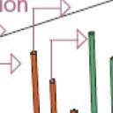
2 Outline Advantages and disadvantages of semiconductor detectors Basic semiconductor properties PN junction Basic silicon detector design Signal formation Position resolution Microstrip vertex detectors Silicon Trackers at LHC Future prospects G.Simi, scuola rivelatori Legnaro 2
3 Advantages of semiconductor detectors Silicon detectors are a kind of solid state ionization chamber 10x lower energy per ionization pair : ~3eV compared to gas (2040 ev/pair) and scintillators ( ev to create a photon) small signal fluctuations High density => Large stopping power compact detectors faster response (~10ns) Smaller diffusion effect (<10 m) better achievable spatial resolution Their use started in the '80s to measure the lifetime of short living particles (charm) Use of planar production technology and integrated circuit readout standard industrial technology cheap G.Simi, scuola rivelatori Legnaro 3
4 Disadvantages of semiconductor detectors No internal amplification small signals needs low noise electronics With a few exceptions High cost per unit surface Silicon bulk material but also interconnects and electronics Large number of readout channels Large power consumption cooling is needed G.Simi, scuola rivelatori Legnaro 4


5
6 Basic Semiconductor Properties G.Simi, scuola rivelatori Legnaro 6
 to reduce thermal generation Cmpound semiconductors IVIV: SiGe, SiC (UV) IIIV: GaAs Nuclear physics gamma IIVI: ZnSe, CdTe (High Z) spectroscopy * usually considered an isolator 25.")
7 Types of semiconductors Elemental semiconductors: Silicon Room temperature Standard industrial technology for integrated circuits Tracking and Vertexing for HEP experiements Germanium Needs cooling (liquid nitrogen) to reduce thermal generation Cmpound semiconductors IVIV: SiGe, SiC (UV) IIIV: GaAs Nuclear physics gamma IIVI: ZnSe, CdTe (High Z) spectroscopy * usually considered an isolator G.Simi, scuola rivelatori Legnaro 7
8 Crystal Structure Many properties relevant for the utilization as detectors are related to the solid state structure of the semiconductor crystal Si, Ge and Diamond* Crystal structure is the diamond lattice Each atom surrounded by four neighbors at the corners of a tetrahedron IIIV es. GaAs Zincblende lattice Two sublattices shifted by one quarter along the diagonal of the cube G.Simi, scuola rivelatori Legnaro 8


9


10


11


12

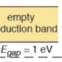
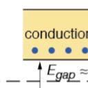
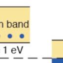
13 Intrinsic carrier concentration Extremely pure semiconductors acre called intrinsic At thermal equilibrium the density of electrons and holes is equal n e =n h =n i The carrier density is Eg 2 n i = Nc Nv e KT T 3/2 e Eg 2 KT Eg 1.12 ev 1.43 ev 0.67 ev For silicon there is ~ 1 electron every atoms The intrinsic Fermi level in a pure semiconductor is near the center of the gap 2 In general even in non pure semicondutors np=n i where n and p are the concentrations for negative and positive carriers G.Simi, scuola rivelatori Legnaro 13
 E For pure Si@300K ρ= 1 e(μ n n μ p p) n= p=1.4510 10 cm 3 ρ=230 k Ωcm How to change the electrical properties, for example increase the conductivity? 25.03.")
14 Carrier mobility and resistivity v e =μ e E v h = μ h E μ e = e τ e m n μ h = e τ h m h m * is the effective mass is the average time between collisions is the mobility For Si@300K μ e =450 cm 2 /Vs μ h =1450 cm 2 /Vs J drift =e(μ n nμ p p) E For pure Si@300K ρ= 1 e(μ n n μ p p) n= p= cm 3 ρ=230 k Ωcm How to change the electrical properties, for example increase the conductivity? G.Simi, scuola rivelatori Legnaro 14
15 Properties summary Material Property Si Ge GaAs GaP CdTe Diamond* Z ;33 31;15 48;52 6 (g/cm 3 ) Eg(eV) at 300K r e at 300K (cm 2 /Vs) h at 300K (cm 2 /Vs) Resistivity 300K( cm) Breakdown field (V/cm) Energy to create eh pair ~ < ~ < ~10 8 ~10 9 > ~ ~ G.Simi, scuola rivelatori Legnaro 15
16 An interesting point G.Simi, scuola rivelatori Legnaro 16

17 An interesting point (cont.) G.Simi, scuola rivelatori Legnaro 17
18 PN Junction G.Simi, scuola rivelatori Legnaro 18
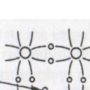
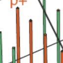
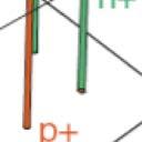
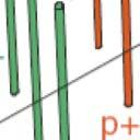
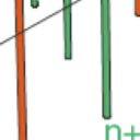
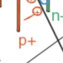
19 Doping Doping consists in adding to pure semiconductor crystal small amounts elements with three(b, Ga, Al, In) or five electrons in the outer shell (P, As, Sb): these are called extrinsic semiconductors They tend to integrate in the lattice forming four covalent bonds with the surrounding silicon atoms therefore: Group III elements (eg B) tend to create holes in the valence band tend to capture electrons in the conduction band; they are called acceptors and the semiconductor is ptype Group V elements (eg P) tend to create electrons in the conduction band and captures holes in the conduction band; they are called donors and the semiconductor is ntype ptype ntype G.Simi, scuola rivelatori Legnaro 19
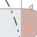
20 Carrier concentration in ptype semicondutors Ptype dopants generate energy levels near the valence band At room temperature they are ionized and increase the hole carriers concentration If the density of dopants is N a >> n i the effective carrier concentration of majority carriers is p = N a The hole concentration (minority carriers) is reduced to n= ni 2/ N a Electron energy Resistivity is reduced to 1/(e N a ) Conduction band Conduction band E C The Fermi level moves close to the valence band E a E V Acceptor level ~0.05eV Valence band Electron energy E C E a E V Valence band Ionized acceptor Fermi energy ~0.05eV G.Simi, scuola rivelatori Legnaro 20
21 Carrier concentration in ntype semicondutors Ntype dopants generate energy levels near the conduction band At room temperature they are ionized and increase the electron carriers concentration If the density of dopants is N d >> n i the effective carrier concentration of majority carriers is n = N d The hole concentration (minority carriers) is reduced to p= ni 2/ N d Electron energy Resistivity is reduced to 1/(e n N d ) Conduction band Conduction band E The Fermi level moves close to ~0.05eV the conduction C band E d Donor level E C E d E V Valence band Electron energy E V Valence band ~0.05eV Fermi energy Ionized donor G.Simi, scuola rivelatori Legnaro 21


22 PN junction ptype ntype We can create a PN junction by diffusing donors and acceptor elements into an intrinsic semiconductor In ptype there is excess positive carriers, in ntype there is excess negative carr G.Simi, scuola rivelatori Legnaro 22
23 PN junction ptype ntype We can create a PN junction by diffusing donors and acceptor elements into a semiconductor At the interface the difference in electron and holes concentration causes diffusion of excessive carriers to the other material until equilibrium is reached and the Fermi energy become the same G.Simi, scuola rivelatori Legnaro 23
24 PN junction ptype Na Nd ntype We can create a PN junction by diffusing donors and acceptor elements into a semiconductor At the interface the difference in electron and holes concentration causes diffusion of excessive carriers to the other material until equilibrium is reached and the Fermi energy become the same The remaining ions create a region of space charge and an electric field which stops further diffusion The charge density is equal to the acceptor and donor densities Na, Nd G.Simi, scuola rivelatori Legnaro 24
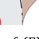
25 PN junction Depletion region ptype Na E Nd ntype We can create a PN junction by diffusing donors and acceptor elements into a semiconductor At the interface the difference in electron and holes concentration causes diffusion of excessive carriers to the other material until equilibrium is reached and the Fermi energy become the same The remaining ions create a region of space charge and an electric field which stops further diffusion In the space charge region there are no free of charge carriers: depletion region G.Simi, scuola rivelatori Legnaro 25
26 PN junction Depletion region ptype Na E Nd ntype Conduction band diffusion E=q V B I ; V BI~ 0.6V (for Si) Electron energy E C E V Valence band Conduction band Fermi energy diffusion Valence band The energy of the bands shift in order to keep the Fermi energy uniform G.Simi, scuola rivelatori Legnaro 26


27
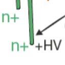
28 Reverse biased PN junction with asymmetric doping Depletion region Na Nd ptype ntype E Na 0 V r Acceptor and donor concentration Nd n x Free carriers concentration p x Space charge Q Q x G.Simi, scuola rivelatori Legnaro 28
29 Reverse biased PN junction with asymmetric doping Depletion region Na Nd ptype ntype E 0 V r Electric field x E=E max en eff ε x Eelctric Potential V r x Space charge Q Q W x W = 2 ε(v r V BI ) en eff G.Simi, scuola rivelatori Legnaro 29
30 Typical PN Junction A typical PN junction in high purity silicon detector Neff(p) = cm 3, Neff(bulk)=10 12 cm 3 Wp=0.2 m, Wbulk=28 m PN junction is reverse biased until the whole depth of the detector is depleted Typical thickness W=300 m Vdepl = 68V Max thickness is given by breakdown voltage Si E BR =310 5 V /cm ; N eff = cm 3 ; W max = ε E BR en eff =2 cm G.Simi, scuola rivelatori Legnaro 30


31


32
33 Basic detector design G.Simi, scuola rivelatori Legnaro 33
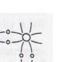
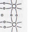
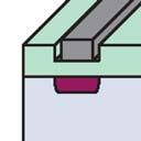
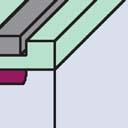
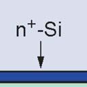
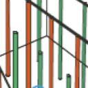
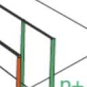
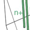
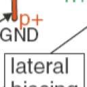
34 A Basic silicon detector Take a pn diode Ptype surface implant Ntype Silicon bulk G.Simi, scuola rivelatori Legnaro 34
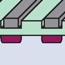
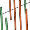
35 A Basic silicon detector Take a pn diode Segment it Ptype surface implant p p p p p p p Add a back contact n Ntype Silicon bulk N Ohmic contact G.Simi, scuola rivelatori Legnaro 35
36 A Basic silicon detector Take a pn diode Segment it Ptype surface implant p p p p p p p Add a back contact Apply reverse voltage Ntype Silicon bulk n N Ohmic contact G.Simi, scuola rivelatori Legnaro 36
37 A Basic silicon detector Take a pn diode Segment it Ptype surface implant p p p p p p p Add a back contact Apply reverse voltage Depletion zone grows from pn junction towards back side Ntype Silicon bulk n N Ohmic contact G.Simi, scuola rivelatori Legnaro 37
38 A Basic silicon detector Take a pn diode Segment it Add a back contact Ptype surface implant p p p p p p p Apply reverse voltage Depletion zone grows from pn junction towards back side Ntype Silicon bulk n N Ohmic contact G.Simi, scuola rivelatori Legnaro 38
39 A Basic silicon detector Take a pn diode Segment it Ptype surface implant p p p p p p p Add a back contact Apply reverse voltage Depletion zone grows from pn junction towards back side Ntype Silicon bulk n N Ohmic contact G.Simi, scuola rivelatori Legnaro 39
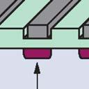
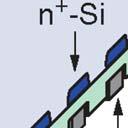
40 A Basic silicon detector Take a pn diode Segment it Add a back contact Apply reverse voltage Depletion zone grows from pn junction towards back side p p p p p p p n Minimum ionizing particle generates electron hole pairs G.Simi, scuola rivelatori Legnaro 40
41 Signal formation and position resolution G.Simi, scuola rivelatori Legnaro 41
42 Ionizing energy loss G.Simi, scuola rivelatori Legnaro 42
43 Ionization signal and Fluctuations in energy loss The energy required to create an electron hole pair is bigger that the bad gap because some energy is lost in vibrations of the lattice Eeh=3.62eV In a thin (300 m) silicon detector the distribution of energy loss is described by a Landau function The Landau function has an asymmetric distribution with tails at large energy losses Most probable value is better defined experimentally Most probable energy loss in 300 m silicon is 79keV = 22'000 pairs 73eh pairs/ m Mean energy loss is 116keV = 32'000 pairs 107eh pairs/ m G.Simi, scuola rivelatori Legnaro 43
44 Intrinsic energy resolution Energy resolution depends on statistical fluctuations of the number of pairs produced Energy loss is due to ionization and lattice exitations However if a particle is completely absorbed the total energy is fixed (event by event) therefore this introduces a correlation between the number of ionizations and the number of lattice excitations. Since the number of phonons is large its relative fluctuation is small As a result the fluctuation in the number of ionizations is smaller than the one derived from Poisson statistics (Ei= energy to create eh pair) σ( E) E = FE i E F~0.1 for Si and Ge E alpha =5MeV (E)=3.5kEV [ignoring electronics noise][check numbers!] G.Simi, scuola rivelatori Legnaro 44
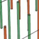
45 A Basic silicon detector Take a pn diode Segment it Add a back contact Apply reverse voltage Depletion zone grows from pn junction towards back side p p p p p p p n E Minimum ionizing particle generates electron hole pairs Charges drift toward the electrodes and induce a signal G.Simi, scuola rivelatori Legnaro 45

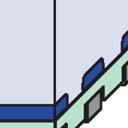
46 A Basic silicon detector Bias resistors to decouple strips R~M p p p p p p p n E G.Simi, scuola rivelatori Legnaro 46
47 A Basic silicon detector Bias resistors to decouple strips R~M Amplify the signal p p p p p p p n E G.Simi, scuola rivelatori Legnaro 47
48 A Basic silicon detector Bias resistors to decouple strips R~M Amplify the signal Add a capacitor to block leakage current SiO2 p p p p p p p n E G.Simi, scuola rivelatori Legnaro 48
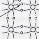
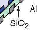
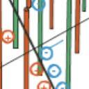
49 Signal formation Moving charge carriers induce a current signal on the electrodes In a simplified parallel plate geometry the induced current is given by the Ramo theorem δq p = q δ x W = δq n I p = q v x W = e μe x W = I n p p p p p p p carriers induce signal when they move both electrons and hole induce a negative current on the p strips and a positive signal on the n strips Current signal is bigger when charge is near p strip because the field is bigger Induced charge is the same for electrons and holes, collection time is different x q v v q n E G.Simi, scuola rivelatori Legnaro 49
50 Signal formation In a strip detector the field is not uniform near the strips so a weighting field has to be used to compute the signal In addition a track transversing the detector creates pairs along the trajectory p p p p p p p n E Collection time can be reduced operating the detector with overbias. Limited by veolicty saturation G.Simi, scuola rivelatori Legnaro 50
51 Position resolution Most important performance parameter of tracking detectors Lmited by Delta rays (already mentioned) Diffusion Binary or analogue readout Strip pitch Signal/noise ratio p p p p p p p n E G.Simi, scuola rivelatori Legnaro 51
; D= KT e μ σ (x)= pitch (12) electrodes diffusion widens the")
52 Resolution for a single strip hit Position resolution More than one strip is hit => cluster Analogue readout allows interpolation between strips => improves resolution Resolution limited by fluctuations due to noise Few m have been obtained in test beams Diffusion While the ionization charge drifts towards the σ D = (2 Dt); D= KT e μ σ (x)= pitch (12) electrodes diffusion widens the cloud of charge Since D~ and t~1/ D is equal for electrons and holes Diffusion acts differently depending on where the ionization is generated G.Simi, scuola rivelatori Legnaro 52

53 Floating strips Strip pitch determines the single strip resolution but requires large number of electronics channels and large power Introduce strip not connected to frontelectronics in between readout strips p p p p p p p n E The signal is transferred by capacitive coupling to the readout strips Use analog readout to recover the position precision Example:pitch 50 m G.Simi, scuola rivelatori Legnaro 53


54

55 Double sided strip detectors Needs also routing for signals Fanout circuits G.Simi, scuola rivelatori Legnaro 55
56 Microstrip vertex detectors G.Simi, scuola rivelatori Legnaro 56
 Resolution of 4.5 m reading out every 3 rd strip 24 cm 2 area Aim: measuring charm lifetime 25.03.15 G.")
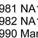
57 Microstrip detectors First strip detector was built by CERN Munich group Was fabricated using a commercial planar process First proof of principle of the use of a position sensitive silicon detector in HEP experiment NA11 (1980) Resolution of 4.5 m reading out every 3 rd strip 24 cm 2 area Aim: measuring charm lifetime G.Simi, scuola rivelatori Legnaro 57

58 Aleph vertex detector G.Simi, scuola rivelatori Legnaro 58

59 Delphi Vertex detector G.Simi, scuola rivelatori Legnaro 59

60 The Power of the Vertex detector (ALEPH) G.Simi, scuola rivelatori Legnaro 60

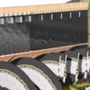
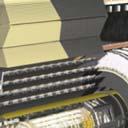
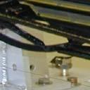
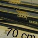
61 BABAR Silicon Vertex Tracker 5 layers Silicon Surface 457cm 2 in L cm 2 in L5 Shift of focus from vertexing to vertexing tracking 70 cm G.Simi, scuola rivelatori Legnaro 61

62 BABAR Silicon Vertex Tracker Double sided nbulk silcon sensors, 630 k cm Double sided nbulk silcon sensors, 630 k cm 5 layers: radius from cm 5 layers: radius from cm Arch shaped outer layer modules to reduce Lrad Stand alone tracking for 70 MeV< pt < 120 MeV Stand alone tracking for 70 MeV< pt < 120 MeV Angular acceptance limited by bending magnets Angular acceptance limited by bending magnets
63 SVT Hit Performance Hit efficiency Hit resolution on z side Hit Efficiency tipically 97% Hit Resolution for pt>1gev/c, wafers Layer 13: 1015 m Layer 45: 3040 m
64 SVT Tracking and PID performance Soft efficiency >70% for pt>50 MeV/c Use pulse height height measurement to extract de/dx 2 separation between kaons and pions up to 500 MeV/c and between kaons and protons up to 1 GeV/c
65 Radiation damage will be the limiting factor to the lifetime of the SVT Two different aspects: A) Radiation damage to the sensors: Instantaneous Creation of pstop shorts => inefficiency From integrated radiation (bulk damage) Increase in leakage current => shot noise Change in the depletion voltage and typeinversion => electronics noise Damages to the crystalline structure => decrease in charge collection efficiency
66 B) Radiation damage to the electronics: Increase in noise => decrease S/N Decrease in gain => decrease S/N Digital failures => inefficiency All these issues have been addressed in the past with projects aimed to quantify the impact on the SVT operation and lifetime
67 Instantaneous radiation damage to the sensors Intense burst of radiation =>discharge of detector capacitor =>Vbias (40V) momentarily drops across the coupling capacitors deposited charge needed Q R = C D ƒ C N C P C N ƒ C P V Bias C2.6 nc / strip on a time scale < = R Bias C det ~1ms => critical radiation: 1 Rad/1 ms
68 Damage Rate All the sensors have been tested for AC breakdown up to 20V during construction A later study on detectors with a pitch similar to the SVT inner layers has shown an expected rate of failures of about 12% The effect has been observed in the real system: 65 pinholes / 20k channels in L1,2
69 Bulk damage: increase in Si leakage current This effects implies an increase in the noise and a potential problem to bias the detector to very high voltages Measuring the leakage current of SVT Si wafers vs. time allows to evaluate the radiation damage IV measurements performed since 1999 Current 40V and the radiation dose estimated from the nearby PIN diode 0.58/0.02 A/Mrad/cm T=17 o C => 1mA hardware limit is not an issue
 C 2 vs V curve indicates typeinversion results in ~ agreement with NIEL scaling hypothesis (not obvious): 3MRad Leakage current increase of order 2")
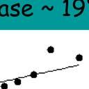
70 Bulk damage: depletion voltage 1/C 2 1/C 2 Voltage (V) Voltage (V) Irradiation with 0.9 GeV e beam at Elettra (Trieste, ) C 2 vs V curve indicates typeinversion results in ~ agreement with NIEL scaling hypothesis (not obvious): 3MRad Leakage current increase of order 2 A/Mrad/cm 2 (T=23 o C) in agreement with measurement in the real SVT After typeinversion up to 5MRad detector electrical properties still look OK


71
72 Noise Prediction Instantaneus damage to Silicon: OK (also for Trickle Inj.) FEE chips damage: signal/noise OK up to 5 Mrad digital funct. OK up to 5 MRad Offset (in progress) Bulk damage to Silicon: V_depl OK up to 10 Mrad I_leak OK > 10 MRad Noise (ENC) SVT SVT layer1 L1Signal/Noise vs do 30 Total S/N Total Noise I leak noise ATOM noise 0 CCE (in progress) Dose (Mrad) Signal/Noise Column B Column E Column F Colum
73 Performance with high background Look at hit efficiency and hit resolution as a function of occupancy in Hit the efficiency FEE Drop off after 20% Hit resolution Slope is 6 m/10% The effect is expected to be significant in 1/10 of layer 1
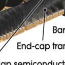
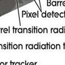
74 LHC Trackers

75 Tevatron and LHC Emphasis shifted from vertexing to tracking in a large volume: CMS vs DELPHI Detector modules, readout electronics and services inside tracking volume material budget constraints
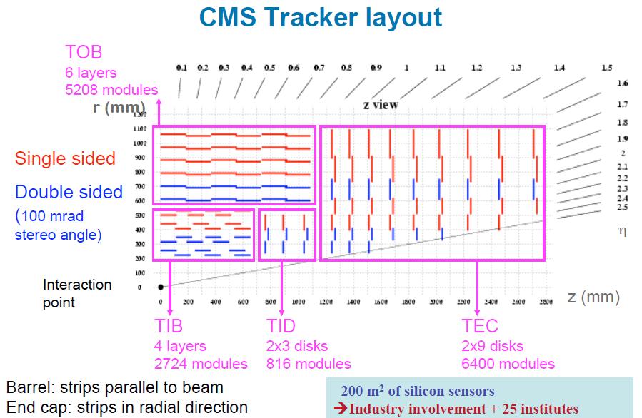
76
77

78 CMS contruction simple process...
 large signal to noise")
79 Pixel detectors The principle of pixel detectors is an array of small independent Si pads Provide unambiguous hit even in high occupancy Small pixel area small capacitance (1fF/pix) large signal to noise (~100:1)


80


81


82


83
84


85
Semiconductor-Detectors
 Semiconductor-Detectors 1 Motivation ~ 195: Discovery that pn-- junctions can be used to detect particles. Semiconductor detectors used for energy measurements ( Germanium) Since ~ 3 years: Semiconductor
Silicon Detectors in High Energy Physics
 Thomas Bergauer (HEPHY Vienna) IPM Teheran 22 May 2011 Sunday: Schedule Silicon Detectors in Semiconductor Basics (45 ) Detector concepts: Pixels and Strips (45 ) Coffee Break Strip Detector Performance
Advantages / Disadvantages of semiconductor detectors
 Advantages / Disadvantages of semiconductor detectors Semiconductor detectors have a high density (compared to gas detector) large energy loss in a short distance diffusion effect is smaller than in gas
Semiconductor Detectors
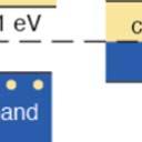
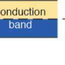
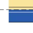
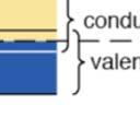
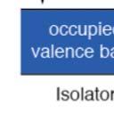
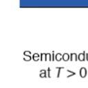
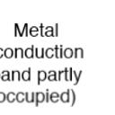
 Semiconductor Detectors Summary of Last Lecture Band structure in Solids: Conduction band Conduction band thermal conductivity: E g > 5 ev Valence band Insulator Charge carrier in conductor: e - Charge
Solid State Detectors Semiconductor detectors Halbleiterdetektoren
 Solid State Detectors Semiconductor detectors Halbleiterdetektoren Doris Eckstein DESY Where are solid state detectors used? > Nuclear Physics: Energy measurement of charged particles (particles up to
Lecture 18. New gas detectors Solid state trackers
 Lecture 18 New gas detectors Solid state trackers Time projection Chamber Full 3-D track reconstruction x-y from wires and segmented cathode of MWPC z from drift time de/dx information (extra) Drift over
Semiconductor Detectors are Ionization Chambers. Detection volume with electric field Energy deposited positive and negative charge pairs
 1 V. Semiconductor Detectors V.1. Principles Semiconductor Detectors are Ionization Chambers Detection volume with electric field Energy deposited positive and negative charge pairs Charges move in field
Chap. 11 Semiconductor Diodes
 Chap. 11 Semiconductor Diodes Semiconductor diodes provide the best resolution for energy measurements, silicon based devices are generally used for charged-particles, germanium for photons. Scintillators
Lecture 2. Introduction to semiconductors Structures and characteristics in semiconductors
 Lecture 2 Introduction to semiconductors Structures and characteristics in semiconductors Semiconductor p-n junction Metal Oxide Silicon structure Semiconductor contact Literature Glen F. Knoll, Radiation
Components of a generic collider detector
 Lecture 24 Components of a generic collider detector electrons - ionization + bremsstrahlung photons - pair production in high Z material charged hadrons - ionization + shower of secondary interactions
Lecture 2. Introduction to semiconductors Structures and characteristics in semiconductors
 Lecture 2 Introduction to semiconductors Structures and characteristics in semiconductors Semiconductor p-n junction Metal Oxide Silicon structure Semiconductor contact Literature Glen F. Knoll, Radiation
Instrumentation for Flavor Physics - Lesson I
 Instrumentation for Flavor Physics - Lesson I! Fisica delle Particelle Università di Milano a.a 2013/2014 Outline Lesson I Introduction Basics for detector design Vertex detectors Lesson II Tracking detectors
Chapter 1 Overview of Semiconductor Materials and Physics
 Chapter 1 Overview of Semiconductor Materials and Physics Professor Paul K. Chu Conductivity / Resistivity of Insulators, Semiconductors, and Conductors Semiconductor Elements Period II III IV V VI 2 B
Lecture 2. Introduction to semiconductors Structures and characteristics in semiconductors. Fabrication of semiconductor sensor
 Lecture 2 Introduction to semiconductors Structures and characteristics in semiconductors Semiconductor p-n junction Metal Oxide Silicon structure Semiconductor contact Fabrication of semiconductor sensor
Experimental Particle Physics
 Experimental Particle Physics Particle Interactions and Detectors Lecture 2 2nd May 2014 Fergus Wilson, RAL 1/31 How do we detect particles? Particle Types Charged (e - /K - /π - ) Photons (γ) Electromagnetic
Semiconductor X-Ray Detectors. Tobias Eggert Ketek GmbH
 Semiconductor X-Ray Detectors Tobias Eggert Ketek GmbH Semiconductor X-Ray Detectors Part A Principles of Semiconductor Detectors 1. Basic Principles 2. Typical Applications 3. Planar Technology 4. Read-out
Solid State Detectors
 Solid State Detectors Most material is taken from lectures by Michael Moll/CERN and Daniela Bortoletto/Purdue and the book Semiconductor Radiation Detectors by Gerhard Lutz. In gaseous detectors, a charged
Experimental Particle Physics
 Experimental Particle Physics Particle Interactions and Detectors Lecture 2 17th February 2010 Fergus Wilson, RAL 1/31 How do we detect particles? Particle Types Charged (e - /K - /π - ) Photons (γ) Electromagnetic
Classification of Solids
 Classification of Solids Classification by conductivity, which is related to the band structure: (Filled bands are shown dark; D(E) = Density of states) Class Electron Density Density of States D(E) Examples
Introduction to Semiconductor Physics. Prof.P. Ravindran, Department of Physics, Central University of Tamil Nadu, India
 Introduction to Semiconductor Physics 1 Prof.P. Ravindran, Department of Physics, Central University of Tamil Nadu, India http://folk.uio.no/ravi/cmp2013 Review of Semiconductor Physics Semiconductor fundamentals
Detectors for High Energy Physics
 Detectors for High Energy Physics Ingrid-Maria Gregor, DESY DESY Summer Student Program 2017 Hamburg July 26th/27th Overview I. Detectors for Particle Physics II. Interaction with Matter } Wednesday III.
Lecture 2. Semiconductor Physics. Sunday 4/10/2015 Semiconductor Physics 1-1
 Lecture 2 Semiconductor Physics Sunday 4/10/2015 Semiconductor Physics 1-1 Outline Intrinsic bond model: electrons and holes Charge carrier generation and recombination Intrinsic semiconductor Doping:
Energetic particles and their detection in situ (particle detectors) Part II. George Gloeckler
 Part II. George Gloeckler") Energetic particles and their detection in situ (particle detectors) Part II George Gloeckler University of Michigan, Ann Arbor, MI University of Maryland, College Park, MD Simple particle detectors Gas-filled
Energetic particles and their detection in situ (particle detectors) Part II George Gloeckler University of Michigan, Ann Arbor, MI University of Maryland, College Park, MD Simple particle detectors Gas-filled
Lecture 1. OUTLINE Basic Semiconductor Physics. Reading: Chapter 2.1. Semiconductors Intrinsic (undoped) silicon Doping Carrier concentrations
 silicon Doping Carrier concentrations") Lecture 1 OUTLINE Basic Semiconductor Physics Semiconductors Intrinsic (undoped) silicon Doping Carrier concentrations Reading: Chapter 2.1 EE105 Fall 2007 Lecture 1, Slide 1 What is a Semiconductor? Low
Lecture 1 OUTLINE Basic Semiconductor Physics Semiconductors Intrinsic (undoped) silicon Doping Carrier concentrations Reading: Chapter 2.1 EE105 Fall 2007 Lecture 1, Slide 1 What is a Semiconductor? Low
Experimental Particle Physics
 Experimental Particle Physics Particle Interactions and Detectors 20th February 2007 Fergus Wilson, RAL 1 How do we detect Particles? Particle Types Charged (e - /K - /π - ) Photons (γ) Electromagnetic
Tracking in High Energy Physics: Silicon Devices!
 Tracking in High Energy Physics: Silicon Devices! G. Leibenguth XIX Graduiertenkolleg Heidelberg 11-12. October 2007 Content Part 1: Basics on semi-conductor Part 2: Construction Part 3: Two Examples Part
PN Junction
 P Junction 2017-05-04 Definition Power Electronics = semiconductor switches are used Analogue amplifier = high power loss 250 200 u x 150 100 u Udc i 50 0 0 50 100 150 200 250 300 350 400 i,u dc i,u u
Chemistry Instrumental Analysis Lecture 8. Chem 4631
 Chemistry 4631 Instrumental Analysis Lecture 8 UV to IR Components of Optical Basic components of spectroscopic instruments: stable source of radiant energy transparent container to hold sample device
Lecture 8. Detectors for Ionizing Particles
 Lecture 8 Detectors for Ionizing Particles Content Introduction Overview of detector systems Sources of radiation Radioactive decay Cosmic Radiation Accelerators Interaction of Radiation with Matter General
Tracking detectors for the LHC. Peter Kluit (NIKHEF)
") Tracking detectors for the LHC Peter Kluit (NIKHEF) Overview lectures part I Principles of gaseous and solid state tracking detectors Tracking detectors at the LHC Drift chambers Silicon detectors Modeling
Tracking detectors for the LHC Peter Kluit (NIKHEF) Overview lectures part I Principles of gaseous and solid state tracking detectors Tracking detectors at the LHC Drift chambers Silicon detectors Modeling
EE 5344 Introduction to MEMS CHAPTER 5 Radiation Sensors
 EE 5344 Introduction to MEMS CHAPTER 5 Radiation Sensors 5. Radiation Microsensors Radiation µ-sensors convert incident radiant signals into standard electrical out put signals. Radiant Signals Classification
Development of Radiation Hard Si Detectors
 Development of Radiation Hard Si Detectors Dr. Ajay K. Srivastava On behalf of Detector Laboratory of the Institute for Experimental Physics University of Hamburg, D-22761, Germany. Ajay K. Srivastava
EECS130 Integrated Circuit Devices
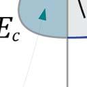
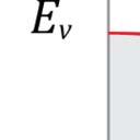
 EECS130 Integrated Circuit Devices Professor Ali Javey 8/30/2007 Semiconductor Fundamentals Lecture 2 Read: Chapters 1 and 2 Last Lecture: Energy Band Diagram Conduction band E c E g Band gap E v Valence
1 Name: Student number: DEPARTMENT OF PHYSICS AND PHYSICAL OCEANOGRAPHY MEMORIAL UNIVERSITY OF NEWFOUNDLAND. Fall :00-11:00
 1 Name: DEPARTMENT OF PHYSICS AND PHYSICAL OCEANOGRAPHY MEMORIAL UNIVERSITY OF NEWFOUNDLAND Final Exam Physics 3000 December 11, 2012 Fall 2012 9:00-11:00 INSTRUCTIONS: 1. Answer all seven (7) questions.
Radiation Detector 2016/17 (SPA6309)
") Radiation Detector 2016/17 (SPA6309) Semiconductor detectors (Leo, Chapter 10) 2017 Teppei Katori Semiconductor detectors are used in many situations, mostly for some kind of high precision measurement.
Radiation Detector 2016/17 (SPA6309) Semiconductor detectors (Leo, Chapter 10) 2017 Teppei Katori Semiconductor detectors are used in many situations, mostly for some kind of high precision measurement.
Chem 481 Lecture Material 3/20/09
 Chem 481 Lecture Material 3/20/09 Radiation Detection and Measurement Semiconductor Detectors The electrons in a sample of silicon are each bound to specific silicon atoms (occupy the valence band). If
Quiz #1 Practice Problem Set
 Name: Student Number: ELEC 3908 Physical Electronics Quiz #1 Practice Problem Set? Minutes January 22, 2016 - No aids except a non-programmable calculator - All questions must be answered - All questions
Semiconductor Physics fall 2012 problems
 Semiconductor Physics fall 2012 problems 1. An n-type sample of silicon has a uniform density N D = 10 16 atoms cm -3 of arsenic, and a p-type silicon sample has N A = 10 15 atoms cm -3 of boron. For each
Semiconductors. SEM and EDAX images of an integrated circuit. SEM EDAX: Si EDAX: Al. Institut für Werkstoffe der ElektrotechnikIWE
 SEM and EDAX images of an integrated circuit SEM EDAX: Si EDAX: Al source: [Cal 99 / 605] M&D-.PPT, slide: 1, 12.02.02 Classification semiconductors electronic semiconductors mixed conductors ionic conductors
Review of Semiconductor Fundamentals
 ECE 541/ME 541 Microelectronic Fabrication Techniques Review of Semiconductor Fundamentals Zheng Yang (ERF 3017, email: yangzhen@uic.edu) Page 1 Semiconductor A semiconductor is an almost insulating material,
ORTEC. Review of the Physics of Semiconductor Detectors. Interaction of Ionizing Radiation with Semiconductor Detectors. Heavy Charged Particles
 ORTEC Review of the Physics of Historically, semiconductor detectors were conceived as solid-state ionization chambers. To obtain a high-electric-field, low-current, solid-state device for detection and
Section 12: Intro to Devices
 Section 12: Intro to Devices Extensive reading materials on reserve, including Robert F. Pierret, Semiconductor Device Fundamentals Bond Model of Electrons and Holes Si Si Si Si Si Si Si Si Si Silicon
Section 12: Intro to Devices
 Section 12: Intro to Devices Extensive reading materials on reserve, including Robert F. Pierret, Semiconductor Device Fundamentals EE143 Ali Javey Bond Model of Electrons and Holes Si Si Si Si Si Si Si
electronics fundamentals
 electronics fundamentals circuits, devices, and applications THOMAS L. FLOYD DAVID M. BUCHLA Lesson 1: Diodes and Applications Semiconductors Figure 1-1 The Bohr model of an atom showing electrons in orbits
The outline. 1) Detector parameters: efficiency, geometrical acceptance, dead-time, resolution, linearity. 2) gaseous ionization chambers
 Detector parameters: efficiency, geometrical acceptance, dead-time, resolution, linearity. 2) gaseous ionization chambers") The outline 1) Detector parameters: efficiency, geometrical acceptance, dead-time, resolution, linearity 2) gaseous ionization chambers 3) proportional counters- ionization measurement 4) silicon detectors
The outline 1) Detector parameters: efficiency, geometrical acceptance, dead-time, resolution, linearity 2) gaseous ionization chambers 3) proportional counters- ionization measurement 4) silicon detectors
Unit IV Semiconductors Engineering Physics
 Introduction A semiconductor is a material that has a resistivity lies between that of a conductor and an insulator. The conductivity of a semiconductor material can be varied under an external electrical
Semiconductor Physics Problems 2015
 Semiconductor Physics Problems 2015 Page and figure numbers refer to Semiconductor Devices Physics and Technology, 3rd edition, by SM Sze and M-K Lee 1. The purest semiconductor crystals it is possible
Epitaxial SiC Schottky barriers for radiation and particle detection
 Epitaxial SiC Schottky barriers for radiation and particle detection M. Bruzzi, M. Bucciolini, R. D'Alessandro, S. Lagomarsino, S. Pini, S. Sciortino INFN Firenze - Università di Firenze F. Nava INFN Bologna
A semiconductor is an almost insulating material, in which by contamination (doping) positive or negative charge carriers can be introduced.
 positive or negative charge carriers can be introduced.") Semiconductor A semiconductor is an almost insulating material, in which by contamination (doping) positive or negative charge carriers can be introduced. Page 2 Semiconductor materials Page 3 Energy levels
Semiconductor A semiconductor is an almost insulating material, in which by contamination (doping) positive or negative charge carriers can be introduced. Page 2 Semiconductor materials Page 3 Energy levels
Junction Diodes. Tim Sumner, Imperial College, Rm: 1009, x /18/2006
 Junction Diodes Most elementary solid state junction electronic devices. They conduct in one direction (almost correct). Useful when one converts from AC to DC (rectifier). But today diodes have a wide
EECS143 Microfabrication Technology
 EECS143 Microfabrication Technology Professor Ali Javey Introduction to Materials Lecture 1 Evolution of Devices Yesterday s Transistor (1947) Today s Transistor (2006) Why Semiconductors? Conductors e.g
CMS Note Mailing address: CMS CERN, CH-1211 GENEVA 23, Switzerland
 Available on CMS information server CMS NOTE 199/11 The Compact Muon Solenoid Experiment CMS Note Mailing address: CMS CERN, CH-1211 GENEVA 23, Switzerland 11 February 199 Temperature dependence of the
KATIHAL FİZİĞİ MNT-510
 KATIHAL FİZİĞİ MNT-510 YARIİLETKENLER Kaynaklar: Katıhal Fiziği, Prof. Dr. Mustafa Dikici, Seçkin Yayıncılık Katıhal Fiziği, Şakir Aydoğan, Nobel Yayıncılık, Physics for Computer Science Students: With
EE301 Electronics I , Fall
 EE301 Electronics I 2018-2019, Fall 1. Introduction to Microelectronics (1 Week/3 Hrs.) Introduction, Historical Background, Basic Consepts 2. Rewiev of Semiconductors (1 Week/3 Hrs.) Semiconductor materials
For the following statements, mark ( ) for true statement and (X) for wrong statement and correct it.
 for true statement and (X) for wrong statement and correct it.") Benha University Faculty of Engineering Shoubra Electrical Engineering Department First Year communications. Answer all the following questions Illustrate your answers with sketches when necessary. The
Benha University Faculty of Engineering Shoubra Electrical Engineering Department First Year communications. Answer all the following questions Illustrate your answers with sketches when necessary. The
Consider a uniformly doped PN junction, in which one region of the semiconductor is uniformly doped with acceptor atoms and the adjacent region is
 CHAPTER 7 The PN Junction Consider a uniformly doped PN junction, in which one region of the semiconductor is uniformly doped with acceptor atoms and the adjacent region is uniformly doped with donor atoms.
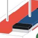
The Hermes Recoil Silicon Detector
 The Hermes Recoil Silicon Detector Introduction Detector design considerations Silicon detector overview TIGRE microstrip sensors Readout electronics Test beam results Vertex 2002 J. Stewart DESY Zeuthen
EE143 Fall 2016 Microfabrication Technologies. Evolution of Devices
 EE143 Fall 2016 Microfabrication Technologies Prof. Ming C. Wu wu@eecs.berkeley.edu 511 Sutardja Dai Hall (SDH) 1-1 Evolution of Devices Yesterday s Transistor (1947) Today s Transistor (2006) 1-2 1 Why
Introduction to Silicon Detectors. G.Villani STFC Rutherford Appleton Laboratory Particle Physics Department
 Introduction to Silicon Detectors G.Villani STFC Rutherford Appleton Laboratory Particle Physics Department 1 Outlook Introduction to physics of Si and detection Examples of detectors Radiation effects
Chapter 7. The pn Junction
 Chapter 7 The pn Junction Chapter 7 PN Junction PN junction can be fabricated by implanting or diffusing donors into a P-type substrate such that a layer of semiconductor is converted into N type. Converting
EEE4106Z Radiation Interactions & Detection
 EEE4106Z Radiation Interactions & Detection 2. Radiation Detection Dr. Steve Peterson 5.14 RW James Department of Physics University of Cape Town steve.peterson@uct.ac.za May 06, 2015 EEE4106Z :: Radiation
Final Examination EE 130 December 16, 1997 Time allotted: 180 minutes
 Final Examination EE 130 December 16, 1997 Time allotted: 180 minutes Problem 1: Semiconductor Fundamentals [30 points] A uniformly doped silicon sample of length 100µm and cross-sectional area 100µm 2
Review of Semiconductor Drift Detectors
 Pavia October 25, 2004 Review of Semiconductor Drift Detectors Talk given by Pavel Rehak following a presentation on 5 th Hiroshima Symposium of Semiconductor Tracking Detectors Outline of the Review Principles
Electro - Principles I
 Electro - Principles I Page 10-1 Atomic Theory It is necessary to know what goes on at the atomic level of a semiconductor so the characteristics of the semiconductor can be understood. In many cases a
D. Meier. representing the RD42 Collaboration. Bristol University, CERN, CPP Marseille, Lawrence Livermore National Lab, LEPSI
 Diamond as a Particle Detector D. Meier representing the RD42 Collaboration Bristol University, CERN, CPP Marseille, Lawrence Livermore National Lab, LEPSI Strasbourg, Los Alamos National Lab, MPIK Heidelberg,
Engineering 2000 Chapter 8 Semiconductors. ENG2000: R.I. Hornsey Semi: 1
 Engineering 2000 Chapter 8 Semiconductors ENG2000: R.I. Hornsey Semi: 1 Overview We need to know the electrical properties of Si To do this, we must also draw on some of the physical properties and we
Midterm I - Solutions
 UNIVERSITY OF CALIFORNIA College of Engineering Department of Electrical Engineering and Computer Sciences EECS 130 Spring 2008 Professor Chenming Hu Midterm I - Solutions Name: SID: Grad/Undergrad: Closed
Silicon Detectors. Particle Physics
 Mitglied der Helmholtz-Gemeinschaft Silicon Detectors for Particle Physics 9. August 2012 Ralf Schleichert, Institut für Kernphysik Outline Different Cameras Silicon Detectors Taking Pictures in Particle
Semiconductor Detectors
 Radiation Measurement Systems Semiconductor Detectors Ho Kyung Kim Pusan National University Semiconductors Differences btwn semiconductor & gas as a material for radiation detectors Higher (1,000 ) Free
physics/ Sep 1997
 GLAS-PPE/97-6 28 August 1997 Department of Physics & Astronomy Experimental Particle Physics Group Kelvin Building, University of Glasgow, Glasgow, G12 8QQ, Scotland. Telephone: +44 - ()141 3398855 Fax:
Session 6: Solid State Physics. Diode
 Session 6: Solid State Physics Diode 1 Outline A B C D E F G H I J 2 Definitions / Assumptions Homojunction: the junction is between two regions of the same material Heterojunction: the junction is between
CMS Note Mailing address: CMS CERN, CH-1211 GENEVA 23, Switzerland
 Available on CMS information server CMS NOTE 1996/005 The Compact Muon Solenoid Experiment CMS Note Mailing address: CMS CERN, CH-1211 GENEVA 23, Switzerland Performance of the Silicon Detectors for the
Introduction to Transistors. Semiconductors Diodes Transistors
 Introduction to Transistors Semiconductors Diodes Transistors 1 Semiconductors Typical semiconductors, like silicon and germanium, have four valence electrons which form atomic bonds with neighboring atoms
Spring Semester 2012 Final Exam
 Spring Semester 2012 Final Exam Note: Show your work, underline results, and always show units. Official exam time: 2.0 hours; an extension of at least 1.0 hour will be granted to anyone. Materials parameters
The photovoltaic effect occurs in semiconductors where there are distinct valence and
 How a Photovoltaic Cell Works The photovoltaic effect occurs in semiconductors where there are distinct valence and conduction bands. (There are energies at which electrons can not exist within the solid)
Chap. 1 (Introduction), Chap. 2 (Components and Circuits)
, Chap. 2 (Components and Circuits)") CHEM 455 The class describes the principles and applications of modern analytical instruments. Emphasis is placed upon the theoretical basis of each type of instrument, its optimal area of application,
CHEM 455 The class describes the principles and applications of modern analytical instruments. Emphasis is placed upon the theoretical basis of each type of instrument, its optimal area of application,
Semiconductor Physics fall 2012 problems
 Semiconductor Physics fall 2012 problems 1. An n-type sample of silicon has a uniform density N D = 10 16 atoms cm -3 of arsenic, and a p-type silicon sample has N A = 10 15 atoms cm -3 of boron. For each
Silicon Detectors in High Energy Physics
 Thomas Bergauer (HEPHY Vienna) IPM Teheran 22 May 2011 Sunday: Schedule Semiconductor Basics (45 ) Silicon Detectors in Detector concepts: Pixels and Strips (45 ) Coffee Break Strip Detector Performance
collisions of electrons. In semiconductor, in certain temperature ranges the conductivity increases rapidly by increasing temperature
 1.9. Temperature Dependence of Semiconductor Conductivity Such dependence is one most important in semiconductor. In metals, Conductivity decreases by increasing temperature due to greater frequency of
Semiconductors. Semiconductors also can collect and generate photons, so they are important in optoelectronic or photonic applications.
 Semiconductors Semiconducting materials have electrical properties that fall between true conductors, (like metals) which are always highly conducting and insulators (like glass or plastic or common ceramics)
smal band gap Saturday, April 9, 2011
 small band gap upper (conduction) band empty small gap valence band filled 2s 2p 2s 2p hybrid (s+p)band 2p no gap 2s (depend on the crystallographic orientation) extrinsic semiconductor semi-metal electron
ECE 340 Lecture 27 : Junction Capacitance Class Outline:
 ECE 340 Lecture 27 : Junction Capacitance Class Outline: Breakdown Review Junction Capacitance Things you should know when you leave M.J. Gilbert ECE 340 Lecture 27 10/24/11 Key Questions What types of
V BI. H. Föll: kiel.de/matwis/amat/semi_en/kap_2/backbone/r2_2_4.html. different electrochemical potentials (i.e.
 Consider the the band diagram for a homojunction, formed when two bits of the same type of semicondutor (e.g. Si) are doped p and ntype and then brought into contact. Electrons in the two bits have different
Atoms? All matters on earth made of atoms (made up of elements or combination of elements).
.") Chapter 1 Atoms? All matters on earth made of atoms (made up of elements or combination of elements). Atomic Structure Atom is the smallest particle of an element that can exist in a stable or independent
Chapter 1 Atoms? All matters on earth made of atoms (made up of elements or combination of elements). Atomic Structure Atom is the smallest particle of an element that can exist in a stable or independent
OPTI510R: Photonics. Khanh Kieu College of Optical Sciences, University of Arizona Meinel building R.626
 OPTI510R: Photonics Khanh Kieu College of Optical Sciences, University of Arizona kkieu@optics.arizona.edu Meinel building R.626 Announcements Homework #6 is assigned, due May 1 st Final exam May 8, 10:30-12:30pm
ELECTRONIC DEVICES AND CIRCUITS SUMMARY
 ELECTRONIC DEVICES AND CIRCUITS SUMMARY Classification of Materials: Insulator: An insulator is a material that offers a very low level (or negligible) of conductivity when voltage is applied. Eg: Paper,
2 The Sensor. 2.1 Introduction. Au: Kindly check wheather all the headings are ok as typeset. Modify if necessary.
 2 The Sensor Abstract. The sensor is the part of the detector system where the interaction with the radiation takes place, and which delivers the signal to the readout electronics. The signal is produced
Ga and P Atoms to Covalent Solid GaP
 Ga and P Atoms to Covalent Solid GaP Band Gaps in Binary Group III-V Semiconductors Mixed Semiconductors Affect of replacing some of the As with P in GaAs Band Gap (ev) (nm) GaAs 1.35 919 (IR) GaP 2.24
Aspects of radiation hardness for silicon microstrip detectors
 Aspects of radiation hardness for silicon microstrip detectors Richard Wheadon, INFN Pisa, Via Livornese 1291, S. Piero a Grado, Pisa, Italy Abstract The ways in which radiation damage affects the properties
Ranjeet Dalal, Ashutosh Bhardwaj, Kirti Ranjan, Kavita Lalwani and Geetika Jain
 Simulation of Irradiated Si Detectors, Ashutosh Bhardwaj, Kirti Ranjan, Kavita Lalwani and Geetika Jain CDRST, Department of physics and Astrophysics, University of Delhi, India E-mail: rdalal@cern.ch
Charge Carriers in Semiconductor
 Charge Carriers in Semiconductor To understand PN junction s IV characteristics, it is important to understand charge carriers behavior in solids, how to modify carrier densities, and different mechanisms
SILICON PARTICLE DETECTOR
 SILICON PARTICLE DETECTOR Supervised Learning Project Eslikumar Adiandhra 12D260012 Department of Physics, IIT Bombay Guide: Prof. Raghava Varma Department of Physics, IIT Bombay November 8, 2015 Abstract
Lecture 9: Metal-semiconductor junctions
 Lecture 9: Metal-semiconductor junctions Contents 1 Introduction 1 2 Metal-metal junction 1 2.1 Thermocouples.......................... 2 3 Schottky junctions 4 3.1 Forward bias............................
Charge Collection and Capacitance-Voltage analysis in irradiated n-type magnetic Czochralski silicon detectors
 Charge Collection and Capacitance-Voltage analysis in irradiated n-type magnetic Czochralski silicon detectors M. K. Petterson, H.F.-W. Sadrozinski, C. Betancourt SCIPP UC Santa Cruz, 1156 High Street,
ET3034TUx Utilization of band gap energy
 ET3034TUx - 3.3.1 - Utilization of band gap energy In the last two weeks we have discussed the working principle of a solar cell and the external parameters that define the performance of a solar cell.
Semiconductor Device Physics
 1 Semiconductor Device Physics Lecture 1 http://zitompul.wordpress.com 2 0 1 3 2 Semiconductor Device Physics Textbook: Semiconductor Device Fundamentals, Robert F. Pierret, International Edition, Addison
Electronics The basics of semiconductor physics
 Electronics The basics of semiconductor physics Prof. Márta Rencz, Gergely Nagy BME DED September 16, 2013 The basic properties of semiconductors Semiconductors conductance is between that of conductors
Semiconductor physics I. The Crystal Structure of Solids
 Lecture 3 Semiconductor physics I The Crystal Structure of Solids 1 Semiconductor materials Types of solids Space lattices Atomic Bonding Imperfection and doping in SOLIDS 2 Semiconductor Semiconductors
Lecture (02) Introduction to Electronics II, PN Junction and Diodes I
 Introduction to Electronics II, PN Junction and Diodes I") Lecture (02) Introduction to Electronics II, PN Junction and Diodes I By: Dr. Ahmed ElShafee ١ Agenda Current in semiconductors/conductors N type, P type semiconductors N Type Semiconductor P Type Semiconductor
Lecture (02) Introduction to Electronics II, PN Junction and Diodes I By: Dr. Ahmed ElShafee ١ Agenda Current in semiconductors/conductors N type, P type semiconductors N Type Semiconductor P Type Semiconductor
Semiconductor Physics and Devices
 The pn Junction 1) Charge carriers crossing the junction. 3) Barrier potential Semiconductor Physics and Devices Chapter 8. The pn Junction Diode 2) Formation of positive and negative ions. 4) Formation