Magnetism and Epitaxy
|
|
|
- Maximillian Davis
- 5 years ago
- Views:
Transcription


1 Integration of Functional Oxides and Semiconductors: Magnetism and Epitaxy Alex Demkov The University of Texas at Austin Texas A&M University, Commerce, November 2013


2 People involved: Hosung Seo Miri Choi Patrick Ponath Kristy Kormondy Agham Posadas Chandrima Mitra Chungwei Lin Richard Hatch
3 Outline of the talk Introduction Magnetism in Oxides Molecular Beam Epitaxy COX LaCoO 3 on Si Conclusions

4 Advances in Oxide Epitaxy
5 Epitaxial oxide on semiconductors BaTiO 3 on Ge SrTiO 3 on Si Model Experiment R. McKee, F. Walker, M. Chisholm, PRL (1998) R. McKee, F. Walker, M. Chisholm, Science 293, 468 (2001)

 H.")
6 SrTiO 3 /LaAlO 3 heterostructure: H. W. Hwang et al., Nature 427, 423 (2004) H. W. Hwang, Science 313, 1895 (2006)


7 N. Reyren et al., Science (2007) A. Brinkman et al., Nature Materials 6, 493 (2007)


8

9 Conceptual structure of the 3-D heterogeneous optoelectronic integrated system-on-silicon for an intelligent vehicle system s variable signal-processing functions depending on the moving speed of the car. K.-W. Lee, A. Noriki, K. Kiyoyama, T. Fukushima, T. Tanaka, and M. Koyanagi, IEEE Trans. Electron Dev. 58, 748 (2011).

10 Diverse Accessible Heterogeneous Integration (DAHI): Compound Semiconductor Materials on Si, Electronic-photonic heterogeneous integration


![Erwin Schrödinger [Ar] =](/docs-images/93/111827552/images/11-3.jpg "1s 2 2s 2 2p 6 3s 2 3p 6")
11 Transition metals A transition metal is one which forms one or more stable ions which have incompletely filled d orbitals. Erwin Schrödinger [Ar] = 1s 2 2s 2 2p 6 3s 2 3p 6 [Ti] = [Ar]3d 2 4s 2 [V] = [Ar]3d 3 4s 2

:")
 t 2g Ligand field theory E S")
12 Perovskite oxides ABO 3 z A - Ligand B O TM y x CaTiO 3, BaTiO 3, SrHfO 3, MO 6 - Count Lev Alekseevich Perovski Octahedral symmetry (O h ): Energy 10 Dq e g High spin Low spin Fe 3+ (d 5 ) t 2g Ligand field theory E S -E T =2J

13 Molecular Orbital Theory M 3d e g * 10 Dq t 2g * e g 10 Dq t 2g O 2p t 2g M 3d e g c O 2p Important energies: crystal filed splitting 10Dq exchange energy J charge transfer energy c


14 Ferroelectricity BaTiO 3 V.L. Ginzburg L.D. Landau B.M. Vul

15 Molecular Beam Epitaxy Epitaxy: ordered growth on a monocrystalline substrate From two Greek words: epi -above and taxis -in ordered manner

16 MBE was invented in the late 1960s at Bell Laboratories by J. R. Arthur and Alfred Y. Cho
17


18 Making Nothing: Vacuum Pumps Torr Torr Torr Torr


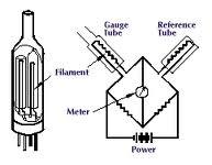
19 Vacuum Chamber Flanges Manipulators Vacuum gauges Transfer rods


20 Knudsen Cell Martin Hans Christian Knudsen ( ) E-gun evaporator


21 Quartz Crystal Monitor Jacques Curie Pierre Curie

22 RHEED

23


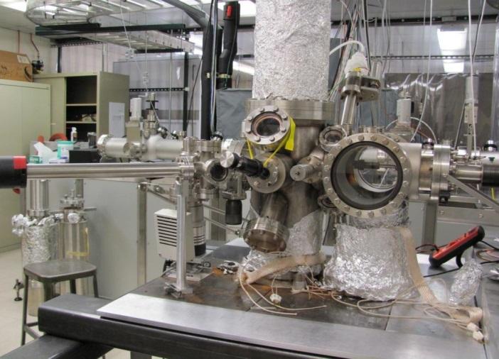

24 Materials Physics Laboratory

 ( ) (")

![ψ = ε + ] [ ]](/docs-images/93/111827552/images/25-3.jpg "[ ] [ ] [ ] [.")


 ( ) (")
 (")


 ( ) (")
25 Theoretical methods i i i i i x m F R E F = = ) ( ) ( ) ( r r r V m i i i ψ ψ = ε + ] [ ] [ ] [ ] [ ] [. n E E n E n E n E H n E XC ion ion ion elec Hartree E K KS = Ψ Ψ = ) ( ) ( ) ( r r r V m i i i KS ψ ψ = ε + ) ( ) ( ) ( ) ( r V dr r r r n r V r V XC ext KS + + = i xc i i i i i xc i i i i V Z V E E Φ Σ Φ + Φ Σ Φ + = ) ( ) ( ε ε ε
 5 0-5 -10 vacuum LAO")
 5 4 LAO LAO")


26 SrTiO 3 /LaAlO 3 heterostructure: 10 Average POT (ev) vacuum LAO STO LAO vacuum Distance along the 001 (A) 5 4 LAO LAO LAO LAO LAO STO STO STO STO STO LAO LAO LAO LAO LAO STO Ti-d orbital 1st interface layer 3 Energy (ev) LAO LAO E F E gsto =3.2eV DOS J.K. Lee and AAD, Phys. Rev. B 78, (2008) Energy (ev)


27 COX: Crystalline oxide on semiconductor BaTiO 3 on Ge SrTiO 3 on Si Model Experiment R. McKee, F. Walker, M. Chisholm, PRL (1998) R. McKee, F. Walker, M. Chisholm, Science 293, 468 (2001)

 0.5 =3.84 Å a STO =3.")
28 A. Geometry: Silicon Si and STO are very different! 45 rotation ABO 3 A-layer B-layer a Si /(2) 0.5 =3.84 Å a STO =3.905 Å B. Chemistry:?

")

29 Zintl intermetallics : SrAl 2 -e Sr Al Al Al Si P Zintl Alchemy Edward Zintl ( ) fcc Al metal SrAl 2 structure ti10 SrAl 4 structure
.")
 Crystallize at 550 C Main SrTiO 3 deposition 4x10⁻⁷ torr O 2 at 550 C Co-evaporation of Sr and Ti at 1 monolayer")
30 SrTiO 3 deposition on Si Sr-assisted SiO 2 desorption Y. Wei et al., J. Vac. Sci. Technol. B 20, 1402 (2002). B. K. Moon and H. Ishiwara, Jpn. J. Appl. Phys., Part 2 33, L472 (1994). ½ monolayer Sr on Si (Zintl template layer) Edward Zintl Initial amorphous SrTiO 3 seed layer at 200 C (4 unit cells) Crystallize at 550 C Main SrTiO 3 deposition 4x10⁻⁷ torr O 2 at 550 C Co-evaporation of Sr and Ti at 1 monolayer per minute 20 unit cells (fully relaxed) STO <110> STO <100>


31 D. Smith, Arizona State 5.98 nm 1.72 nm J. Bruley and C. Dubourdieu, IBM
32 Integrating ferromagnets on Si (001) 7.0x x10-5 Magnetic moment (emu) 5.0x x x x x Temperature (K) Magnetic moment (µ B /Co) Magnetic field (koe)
33 Properties and applications La 1-x Sr x CoO 3 Properties Co 3+ : 3d ev gap semiconductor Non-magnetic at low temperature but paramagnetic at room temperature Epitaxial strain induces ferromagnetism* Spin state transitions Low, intermediate, high-spin Metal-insulator transition when doped Possible applications Electrode (Sr-doped) Cathode material for solid oxide fuel cells Epitaxial oxide electrode for perovskite multilayers Gas sensors / catalysis Magnetic semiconductor Spintronics t 2g e g Fuchs et al., PRB 75, (2007) Rondinelli&Spaldin, PRB 79, (2009) NO Gupta&Mahadevan, PRB 79, (2009) YES
 S = 1 High")
 E F e g * (W 4 ev) *Low")
34 LaCoO 3 Low spin (LS) S = 0 Intermediate spin (IS) S = 1 High spin (HS) S = 2 t 2g * (W 1.5 ev) E F e g * (W 4 ev) *Low spin (LS); S = 0
35 Energy vs. strain DOS (a.u.) Energy (ev/cell) d(yz) / d(xz) t 2g* e g * NM (a - a - c 0 ) NM (a 0 a 0 c - ) NM (a - a - c - ) Homo. IS Strain (%) Energy (ev) d(yz) / d(xz) IS e g * t 2g * Half-metallic IS is stabilized beyond 3.8%. Experimentally, strained LCO on STO is insulating. Experimental critical strain is less than 3.8%.
36 Issues related to MBE growth of LCO on Si Direct deposition of La, Co on Si in oxygen at high temperature will form CoSi 2 and SiO 2 Incommensurate or amorphous Prevents epitaxy Phase formation range of LaCoO 3 requires both high oxygen chemical potential and high temperature Typical MBE growth conditions using molecular oxygen (10-6 torr) results in Co 2+ oxidation state To overcome these difficulties we will use an SrTiO 3 /Si pseudo substrate Use an epitaxial template layer SrTiO 3 on Si Use activated oxygen atomic oxygen from rf plasma source

37 Growth of LaCoO 3 on STO/silicon Atomic oxygen 300 W rf power 1x10⁻⁵ torr background oxygen pressure Substrate temperature 750 C Co-deposition of La and Co with matched fluxes 2 unit cells per minute rate Slow cooling in oxygen 10 C per minute to 100 C LCO <110> LCO <100>

38 Cross-section TEM LaCoO 3 8 nm SrTiO 3 6 nm SiO 2 Si
39 X-ray diffraction 30 nm LCO/8 nm STO/Si Core level spectra (XPS) La 3d 3/2 La 3d 5/2 O 1s Co 2p La 3d Intensity (a.u.) Co 2p 1/2 Co 2p 3/2 O 1s No secondary phases (La 4 Co 3 O 10,La 2 CoO 4, CoO) LaCoO 3 lattice parameters (bulk a = 3.80 Å) c = 3.77 Å a = 3.89 Å Strained to SrTiO 3 (a = 3.90 Å) Binding energy (ev) No Co metal detected in XPS Spectra consistent with literature data for single crystal
40 Magnetization vs. temperature 7.0x x10-5 H = 1 koe Field cooled Magnetic moment (emu) 5.0x x x x x T C = 85 K Temperature (K)
41 Magnetization vs. field T = 10 K Magnetic moment (µ B /Co) Magnetic field (koe) Posadas, et al., Appl. Phys. Lett. 98, , (2011).
42 Energy vs. strain DOS (a.u.) Energy (ev/cell) d(yz) / d(xz) t 2g* e g * NM (a - a - c 0 ) NM (a 0 a 0 c - ) NM (a - a - c - ) Homo. IS Strain (%) Energy (ev) d(yz) / d(xz) IS e g * t 2g * Half-metallic IS is stabilized beyond 3.8%. Experimentally, strained LCO on STO is insulating. Experimental critical strain is less than 3.8%.


43 Supercells independent Co sites 2 in-plane, 2 out-of-plane Identical site - 8 independent Co sites 2 in-plane, 4 out-of-plane - 8 independent Co sites 4 in-plane, 2 out-of-plane

 HS/LS (1:1) 1.0 0.")
")
44 Energy vs. strain: HS/LS mixed states Energy (ev/cell) 1.2 Non-magnetic Homo. IS HS/LS (1:3) HS/LS (1:1) Strain (%) Seo, et al., Phys. Rev. B 86, (2012). 3.8% 2.5%
45 Band gap change as a function of strain Energy (ev) strain (%) d x 2 -y 2 d 3z 2 -r 2 d xy d yz, d xz D 4h Compressive Cubic, O h D 4h Tensile d 3z 2 -r d 2 x 2 -y 2 d yz, d xz d xy

 TD = -4 b + b / 2-2 0 2 4 in out Δ TD (%)")
46 Strain accommodation LaCoO 3 SrTiO 3 Corner-sharing octahedral network with relatively rigid CoO 6 units under epitaxial stress c a b out b -3 in -6-9 ( bin bout ) TD = -4 b + b / in out Δ TD (%) strain (%)
 θ out ( ) 182 175 168 161 154 NM HS/LS θ 0 = 162.")
47 Bond lengths and angles Δ TD (%) NM HS site LS site strain (%) θ in ( ) θ 0 = NM HS/LS strain (%) θ out ( ) NM HS/LS θ 0 = strain (%)


48 Voltage-switchable magnetoresistance in LaCoO 3 SEM image of device Normally nonmagnetic LaCoO 3 becomes ferromagnetic below 85 K under tensile strain No magnetoresistance above T C for both voltage polarities Magnetoresistance observed only below T C and for only positive voltage Critical voltage needed to observe magentoresistance In collaboration with Ed Yu, UT Austin
49 Summary First demonstration of epitaxial growth of magnetic LaCoO 3 on silicon. High quality crystalline LaCoO 3 layer epitaxially strained to underlying SrTiO 3 buffer (XRD, TEM, XPS), T C ~ 85 K (SQUID) Beyond biaxial tensile strain of 2.5% local magnetic moments, originating from HS (S=2) states of Co 3+ ions, emerge in the LS Co 3+ matrix. The HS/LS state is insulating. The stabilization of the FM state is attributed to increased compliance of LCO when it has higher concentration of HS Co 3+ ions. Despite the energy cost to excite LS Co 3+ to HS state, LCO chooses this option and gains energy above tensile strain of 2.5% owing to the softness of the HS CoO 6 clusters. In contrast, compressive strain could not produce a magnetic state in LCO.
JOHN G. EKERDT RESEARCH FOCUS
 JOHN G. EKERDT RESEARCH FOCUS We study the surface, growth and materials chemistry of ultrathin metal and dielectric films. Our work seeks to: 1) develop and understand the reactions and chemistry that
JOHN G. EKERDT RESEARCH FOCUS
 JOHN G. EKERDT RESEARCH FOCUS We study the surface, growth and materials chemistry of metal, dielectric, ferroelectric, and polymer thin films. We seek to understand and describe nucleation and growth
What so special about LaAlO3/SrTiO3 interface? Magnetism, Superconductivity and their coexistence at the interface
 What so special about LaAlO3/SrTiO3 interface? Magnetism, Superconductivity and their coexistence at the interface Pramod Verma Indian Institute of Science, Bangalore 560012 July 24, 2014 Pramod Verma
2D MBE Activities in Sheffield. I. Farrer, J. Heffernan Electronic and Electrical Engineering The University of Sheffield
 2D MBE Activities in Sheffield I. Farrer, J. Heffernan Electronic and Electrical Engineering The University of Sheffield Outline Motivation Van der Waals crystals The Transition Metal Di-Chalcogenides
1 Corresponding author:
 Scanning Tunneling Microscopy Study of Cr-doped GaN Surface Grown by RF Plasma Molecular Beam Epitaxy Muhammad B. Haider, Rong Yang, Hamad Al-Brithen, Costel Constantin, Arthur R. Smith 1, Gabriel Caruntu
Nanoxide electronics
 Nanoxide electronics Alexey Kalabukhov Quantum Device Physics Laboratory MC2, room D515 Alexei.kalaboukhov@chalmers.se Playing Lego with oxide materials: G. Rijnders, D.H.A. Blank, Nature 433, 369 (2005)
Fabrication and Characteristic Investigation of Multifunctional Oxide p-n Heterojunctions
 Advances in Science and Technology Vol. 45 (2006) pp. 2582-2587 online at http://www.scientific.net (2006) Trans Tech Publications, Switzerland Fabrication and Characteristic Investigation of Multifunctional
Aberration-corrected TEM studies on interface of multilayered-perovskite systems
 Aberration-corrected TEM studies on interface of multilayered-perovskite systems By Lina Gunawan (0326114) Supervisor: Dr. Gianluigi Botton November 1, 2006 MSE 702(1) Presentation Outline Literature Review
Spin pumping in Ferromagnet-Topological Insulator-Ferromagnet Heterostructures Supplementary Information.
 Spin pumping in Ferromagnet-Topological Insulator-Ferromagnet Heterostructures Supplementary Information. A.A. Baker,, 2 A.I. Figueroa, 2 L.J. Collins-McIntyre, G. van der Laan, 2 and T., a) Hesjedal )
Department of Electrical Engineering and Information Systems, Tanaka-Ohya lab.
 Observation of the room-temperature local ferromagnetism and its nanoscale expansion in the ferromagnetic semiconductor Ge 1 xfe x Yuki K. Wakabayashi 1 and Yukio Takahashi 2 1 Department of Electrical
Harvesting Heat through Seebeck Spin Tunneling Effect
 Harvesting Heat through Seebeck Spin Tunneling Effect Costel Constantin James Madison University Science Enabled by Photon Source, May 2012 Outline 1. Spintronics vs. Spin Caloritronics. 2. Novel Spin
X-Ray Photoelectron Spectroscopy (XPS) Prof. Paul K. Chu
 Prof. Paul K. Chu") X-Ray Photoelectron Spectroscopy (XPS) Prof. Paul K. Chu X-ray Photoelectron Spectroscopy Introduction Qualitative analysis Quantitative analysis Charging compensation Small area analysis and XPS imaging
X-Ray Photoelectron Spectroscopy (XPS) Prof. Paul K. Chu X-ray Photoelectron Spectroscopy Introduction Qualitative analysis Quantitative analysis Charging compensation Small area analysis and XPS imaging
Nanoxide electronics
 Nanoxide electronics Alexey Kalabukhov Quantum Device Physics Laboratory MC2, room D515 Alexei.kalaboukhov@chalmers.se Playing Lego with oxide materials: G. Rijnders, D.H.A. Blank, Nature 433, 369 (2005)
Influence of Size on the Properties of Materials
 Influence of Size on the Properties of Materials M. J. O Shea Kansas State University mjoshea@phys.ksu.edu If you cannot get the papers connected to this work, please e-mail me for a copy 1. General Introduction
Solid State Science and Technology, Vol. 13, No 1 & 2 (2005) ISSN
 ISSN") FABRICATION OF Bi-Ti-O THIN FILM PRESSURE SENSOR PREPARED BY ELECTRON BEAM EVAPORATION METHOD Chong Cheong Wei, Muhammad Yahaya and Muhamad Mat Salleh Institue of Microengineering and Nanoelectronics,
FABRICATION OF Bi-Ti-O THIN FILM PRESSURE SENSOR PREPARED BY ELECTRON BEAM EVAPORATION METHOD Chong Cheong Wei, Muhammad Yahaya and Muhamad Mat Salleh Institue of Microengineering and Nanoelectronics,
Outline. Introduction: graphene. Adsorption on graphene: - Chemisorption - Physisorption. Summary
 Outline Introduction: graphene Adsorption on graphene: - Chemisorption - Physisorption Summary 1 Electronic band structure: Electronic properties K Γ M v F = 10 6 ms -1 = c/300 massless Dirac particles!
in this web service Cambridge University Press
 High-k Materials Mat. Res. Soc. Symp. Proc. Vol. 670 2001 Materials Research Society Materials and Physical Properties of Novel High-k and Medium-k Gate Dielectrics Ran Liu, Stefan Zollner, Peter Fejes,
SUPPLEMENTARY INFORMATION
 Titanium d xy ferromagnetism at the LaAlO 3 /SrTiO 3 interface J.-S. Lee 1,*, Y. W. Xie 2, H. K. Sato 3, C. Bell 3, Y. Hikita 3, H. Y. Hwang 2,3, C.-C. Kao 1 1 Stanford Synchrotron Radiation Lightsource,
Studying Metal to Insulator Transitions in Solids using Synchrotron Radiation-based Spectroscopies.
 PY482 Lecture. February 28 th, 2013 Studying Metal to Insulator Transitions in Solids using Synchrotron Radiation-based Spectroscopies. Kevin E. Smith Department of Physics Department of Chemistry Division
TMT4320 Nanomaterials November 10 th, Thin films by physical/chemical methods (From chapter 24 and 25)
") 1 TMT4320 Nanomaterials November 10 th, 2015 Thin films by physical/chemical methods (From chapter 24 and 25) 2 Thin films by physical/chemical methods Vapor-phase growth (compared to liquid-phase growth)
1 TMT4320 Nanomaterials November 10 th, 2015 Thin films by physical/chemical methods (From chapter 24 and 25) 2 Thin films by physical/chemical methods Vapor-phase growth (compared to liquid-phase growth)
MSE 321 Structural Characterization
 Auger Spectroscopy Auger Electron Spectroscopy (AES) Scanning Auger Microscopy (SAM) Incident Electron Ejected Electron Auger Electron Initial State Intermediate State Final State Physical Electronics
Holcomb Group Capabilities
 Holcomb Group Capabilities Synchrotron Radiation & Ultrafast Optics West Virginia University mikel.holcomb@mail.wvu.edu The Physicists New Playground The interface is the device. - Herbert Kroemer, beginning
Magnetic Circular Dichroism spectroscopy in epitaxial La 0.7 Sr 0.3 MnO 3 thin films
 Magnetic Circular Dichroism spectroscopy in epitaxial La 0.7 Sr 0.3 MnO 3 thin films T. K. Nath 1 and J. R. Neal 2, G. A. Gehring 2 1 Dept. of Physics and Meteorology, Indian Institute Technology of Kharagpur,
Stripes developed at the strong limit of nematicity in FeSe film
 Stripes developed at the strong limit of nematicity in FeSe film Wei Li ( ) Department of Physics, Tsinghua University IASTU Seminar, Sep. 19, 2017 Acknowledgements Tsinghua University Prof. Qi-Kun Xue,
Material Science II. d Electron systems
 Material Science II. d Electron systems 1. Electronic structure of transition-metal ions (May 23) 2. Crystal structure and band structure (June 13) 3. Mott s (June 20) 4. Metal- transition (June 27) 5.
Research Highlights. Salient results from our group. Mixed phosphides in Sn-P and Sn-Mn-P systems
 Research Highlights Dilute magnetic semiconductors and Spintronics Spintronics is a branch of electronics emerged from the dilute magnetic semiconductor in an aspect of utilization of the spin in addition
Strain-induced single-domain growth of epitaxial SrRuO 3 layers on SrTiO 3 : a high-temperature x-ray diffraction study
 Strain-induced single-domain growth of epitaxial SrRuO 3 layers on SrTiO 3 : a high-temperature x-ray diffraction study Arturas Vailionis 1, Wolter Siemons 1,2, Gertjan Koster 1 1 Geballe Laboratory for
Origin of Metallic States at Heterointerface between Band Insulators LaAlO 3 and SrTiO 3
 Origin of Metallic States at Heterointerface between Band Insulators LaAlO 3 and SrTiO 3 K. Yoshimatsu 1, R. Yasuhara 1, H. Kumigashira 1, 2, *, and M. Oshima 1, 2 1 Department of Applied Chemistry, University
Chris G. Van de Walle
 Complex oxide interfaces Chris G. Van de Walle Anderson Janotti, Lars Bjaalie, Luke Gordon, Burak Himmetoglu, K. Krishnaswamy Materials Department, University of California, Santa Barbara ES213 June 11-14,
STRUCTURAL AND MAGNETOTRANSPORT STUDY OF SrTiO 3-δ /Si STRUCTURES GROWN BY MOLECULAR BEAM EPITAXY. Daniel Alexander Currie, B.S.
 STRUCTURAL AND MAGNETOTRANSPORT STUDY OF SrTiO 3-δ /Si STRUCTURES GROWN BY MOLECULAR BEAM EPITAXY By Daniel Alexander Currie, B.S. A thesis submitted to the Graduate Council of Texas State University in
Angle-Resolved Two-Photon Photoemission of Mott Insulator
 Angle-Resolved Two-Photon Photoemission of Mott Insulator Takami Tohyama Institute for Materials Research (IMR) Tohoku University, Sendai Collaborators IMR: H. Onodera, K. Tsutsui, S. Maekawa H. Onodera
Making the Invisible Visible: Probing Antiferromagnetic Order in Novel Materials
 Making the Invisible Visible: Probing Antiferromagnetic Order in Novel Materials Elke Arenholz Lawrence Berkeley National Laboratory Antiferromagnetic contrast in X-ray absorption Ni in NiO Neel Temperature
High resolution ion beam analysis. Torgny Gustafsson
 High resolution ion beam analysis Torgny Gustafsson Review articles and Books L. C. Feldman, J. W. Mayer and S. T. Picraux, Materials Analysis by Ion Channeling, Academic Press (1982) I. Stensgaard, Surface
Spettroscopia risonante di stati elettronici: un approccio impossibile senza i sincrotroni
 Spettroscopia risonante di stati elettronici: un approccio impossibile senza i sincrotroni XAS, XMCD, XES, RIXS, ResXPS: introduzione alle spettroscopie risonanti * Dipartimento di Fisica - Politecnico
Electronic structure calculations results from LDA+U method
 Electronic structure calculations results from LDA+U method Vladimir I. Anisimov Institute of Metal Physics Ekaterinburg, Russia LDA+U method applications Mott insulators Polarons and stripes in cuprates
Supplementary Figure 1 SEM image for the bulk LCO.
 Supplementary Figure 1 SEM image for the bulk LCO. S1 Supplementary Figure 2 TEM and HRTEM images of LCO nanoparticles. (a)-(c) TEM, HRTEM images, and SAED pattern for the 60 nm LCO, respectively. (d)-(f)
Ferromagnetism and Anomalous Hall Effect in Graphene
 Ferromagnetism and Anomalous Hall Effect in Graphene Jing Shi Department of Physics & Astronomy, University of California, Riverside Graphene/YIG Introduction Outline Proximity induced ferromagnetism Quantized
Room-temperature tunable microwave properties of strained SrTiO 3 films
 JOURNAL OF APPLIED PHYSICS VOLUME 96, NUMBER 11 1 DECEMBER 2004 Room-temperature tunable microwave properties of ed SrTiO 3 films Wontae Chang, a) Steven W. Kirchoefer, Jeffrey M. Pond, Jeffrey A. Bellotti,
Supplementary Figure 1 Comparison between normalized and unnormalized reflectivity of
 Supplementary Figures Supplementary Figure 1 Comparison between normalized and unnormalized reflectivity of bulk SrTiO 3. The normalized high-energy reflectivity (0.5 35 ev) of SrTiO 3 is compared to the
Physics of Semiconductors
 Physics of Semiconductors 9 th 2016.6.13 Shingo Katsumoto Department of Physics and Institute for Solid State Physics University of Tokyo Site for uploading answer sheet Outline today Answer to the question
Challenges for Materials to Support Emerging Research Devices
 Challenges for Materials to Support Emerging Research Devices C. Michael Garner*, James Hutchby +, George Bourianoff*, and Victor Zhirnov + *Intel Corporation Santa Clara, CA + Semiconductor Research Corporation
Magnetism in correlated-electron materials
 Magnetism in correlated-electron materials B. Keimer Max-Planck-Institute for Solid State Research focus on delocalized electrons in metals and superconductors localized electrons: Hinkov talk outline
Energy Spectroscopy. Ex.: Fe/MgO
 Energy Spectroscopy Spectroscopy gives access to the electronic properties (and thus chemistry, magnetism,..) of the investigated system with thickness dependence Ex.: Fe/MgO Fe O Mg Control of the oxidation
Challenges and Opportunities. Prof. J. Raynien Kwo 年
 Nanoelectronics Beyond Si: Challenges and Opportunities Prof. J. Raynien Kwo 年 立 Si CMOS Device Scaling Beyond 22 nm node High κ,, Metal gates, and High mobility channel 1947 First Transistor 1960 1960
TRANSVERSE SPIN TRANSPORT IN GRAPHENE
 International Journal of Modern Physics B Vol. 23, Nos. 12 & 13 (2009) 2641 2646 World Scientific Publishing Company TRANSVERSE SPIN TRANSPORT IN GRAPHENE TARIQ M. G. MOHIUDDIN, A. A. ZHUKOV, D. C. ELIAS,
Rashba spin-orbit coupling in the oxide 2D structures: The KTaO 3 (001) Surface
 Surface") Rashba spin-orbit coupling in the oxide 2D structures: The KTaO 3 (001) Surface Sashi Satpathy Department of Physics University of Missouri, Columbia, USA E Ref: K. V. Shanavas and S. Satpathy, Phys. Rev.
Rashba spin-orbit coupling in the oxide 2D structures: The KTaO 3 (001) Surface Sashi Satpathy Department of Physics University of Missouri, Columbia, USA E Ref: K. V. Shanavas and S. Satpathy, Phys. Rev.
Spectroscopy of correlated electrons in nickelates and titanates
 Spectroscopy of correlated electrons in nickelates and titanates Metal-insulator transitions and novel 2DEGs Dept. of Physics University of CA, Santa Barbara Strong Electron Correlations Materials which
arxiv:cond-mat/ v1 [cond-mat.mtrl-sci] 7 Feb 2002
![arxiv:cond-mat/ v1 [cond-mat.mtrl-sci] 7 Feb 2002](/thumbs/92/108939501.jpg "arxiv:cond-mat/ v1 [cond-mat.mtrl-sci] 7 Feb 2002") Electronic structures of doped anatase TiO : Ti x M x O (M=Co, Mn, Fe, Ni) Min Sik Park, S. K. Kwon, and B. I. Min Department of Physics and electron Spin Science Center, Pohang University of Science and
Electronic structures of doped anatase TiO : Ti x M x O (M=Co, Mn, Fe, Ni) Min Sik Park, S. K. Kwon, and B. I. Min Department of Physics and electron Spin Science Center, Pohang University of Science and
Recent Developments in Magnetoelectrics Vaijayanti Palkar
 Recent Developments in Magnetoelectrics Vaijayanti Palkar Department of Condensed Matter Physics & Materials Science Tata Institute of Fundamental Research Mumbai 400 005, India. Tata Institute of Fundamental
Temperature dependence of spin diffusion length in silicon by Hanle-type spin. precession
 Temperature dependence of spin diffusion length in silicon by Hanle-type spin precession T. Sasaki 1,a), T. Oikawa 1, T. Suzuki 2, M. Shiraishi 3, Y. Suzuki 3, and K. Noguchi 1 SQ Research Center, TDK
Epitaxial piezoelectric heterostructures for ultrasound micro-transducers
 15 th Korea-U.S. Forum on Nanotechnology Epitaxial piezoelectric heterostructures for ultrasound micro-transducers Seung-Hyub Baek Center for Electronic Materials Korea Institute of Science and Technology
Solid Surfaces, Interfaces and Thin Films
 Hans Lüth Solid Surfaces, Interfaces and Thin Films Fifth Edition With 427 Figures.2e Springer Contents 1 Surface and Interface Physics: Its Definition and Importance... 1 Panel I: Ultrahigh Vacuum (UHV)
Thermal Stress and Strain in a GaN Epitaxial Layer Grown on a Sapphire Substrate by the MOCVD Method
 CHINESE JOURNAL OF PHYSICS VOL. 48, NO. 3 June 2010 Thermal Stress and Strain in a GaN Epitaxial Layer Grown on a Sapphire Substrate by the MOCVD Method H. R. Alaei, 1 H. Eshghi, 2 R. Riedel, 3 and D.
SEMICONDUCTOR GROWTH TECHNIQUES. Introduction to growth techniques (bulk, epitaxy) Basic concepts in epitaxy (MBE, MOCVD)
 Basic concepts in epitaxy (MBE, MOCVD)") SEMICONDUCTOR GROWTH TECHNIQUES Introduction to growth techniques (bulk, epitaxy) Basic concepts in epitaxy (MBE, MOCVD) Growth Processes Bulk techniques (massive semiconductors, wafers): Si, compounds
SEMICONDUCTOR GROWTH TECHNIQUES Introduction to growth techniques (bulk, epitaxy) Basic concepts in epitaxy (MBE, MOCVD) Growth Processes Bulk techniques (massive semiconductors, wafers): Si, compounds
Center for Integrated Nanostructure Physics (CINAP)
") Center for Integrated Nanostructure Physics (CINAP) - Institute for Basic Science (IBS) was launched in 2012 by the Korean government to promote basic science in Korea - Our Center was established in 2012
Center for Integrated Nanostructure Physics (CINAP) - Institute for Basic Science (IBS) was launched in 2012 by the Korean government to promote basic science in Korea - Our Center was established in 2012
Rh 3d. Co 2p. Binding Energy (ev) Binding Energy (ev) (b) (a)
 Binding Energy (ev) (b) (a)") Co 2p Co(0) 778.3 Rh 3d Rh (0) 307.2 810 800 790 780 770 Binding Energy (ev) (a) 320 315 310 305 Binding Energy (ev) (b) Supplementary Figure 1 Photoemission features of a catalyst precursor which was
Co 2p Co(0) 778.3 Rh 3d Rh (0) 307.2 810 800 790 780 770 Binding Energy (ev) (a) 320 315 310 305 Binding Energy (ev) (b) Supplementary Figure 1 Photoemission features of a catalyst precursor which was
Structure analysis: Electron diffraction LEED TEM RHEED
 Structure analysis: Electron diffraction LEED: Low Energy Electron Diffraction SPA-LEED: Spot Profile Analysis Low Energy Electron diffraction RHEED: Reflection High Energy Electron Diffraction TEM: Transmission
When transition metals are incorporated into a certain site of the BiT, some of BiT-LaTMO 3
 Band gap tuning in ferroelectric Bi 4 Ti 3 O 12 by alloying LaTMO 3 (TM = Ti, V, Cr, Mn, Co, Ni, and Al) Woo Seok Choi and Ho Nyung Lee Materials Science and Technology Division, Oak Ridge National Laboratory,
Nanoelectronics 09. Atsufumi Hirohata Department of Electronics. Quick Review over the Last Lecture
 Nanoelectronics 09 Atsufumi Hirohata Department of Electronics 13:00 Monday, 12/February/2018 (P/T 006) Quick Review over the Last Lecture ( Field effect transistor (FET) ): ( Drain ) current increases
Thin Film Bi-based Perovskites for High Energy Density Capacitor Applications
 ..SKELETON.. Thin Film Bi-based Perovskites for High Energy Density Capacitor Applications Colin Shear Advisor: Dr. Brady Gibbons 2010 Table of Contents Chapter 1 Introduction... 1 1.1 Motivation and Objective...
Proximity-induced magnetization dynamics, interaction effects, and phase transitions on a topological surface
 Proximity-induced magnetization dynamics, interaction effects, and phase transitions on a topological surface Ilya Eremin Theoretische Physik III, Ruhr-Uni Bochum Work done in collaboration with: F. Nogueira
single-layer transition metal dichalcogenides MC2
 single-layer transition metal dichalcogenides MC2 Period 1 1 H 18 He 2 Group 1 2 Li Be Group 13 14 15 16 17 18 B C N O F Ne 3 4 Na K Mg Ca Group 3 4 5 6 7 8 9 10 11 12 Sc Ti V Cr Mn Fe Co Ni Cu Zn Al Ga
A new era in surface diffraction pulsed laser deposition of complex metal oxide thin films
 A new era in surface diffraction pulsed laser deposition of complex metal oxide thin films Phil Willmott, Christian Schlepütz tz,, Roger Herger, Oliver Bunk, and Bruce Patterson Beamline X04SA Materials
Basics of DFT applications to solids and surfaces
 Basics of DFT applications to solids and surfaces Peter Kratzer Physics Department, University Duisburg-Essen, Duisburg, Germany E-mail: Peter.Kratzer@uni-duisburg-essen.de Periodicity in real space and
Direct observation of a Ga adlayer on a GaN(0001) surface by LEED Patterson inversion. Xu, SH; Wu, H; Dai, XQ; Lau, WP; Zheng, LX; Xie, MH; Tong, SY
 surface by LEED Patterson inversion. Xu, SH; Wu, H; Dai, XQ; Lau, WP; Zheng, LX; Xie, MH; Tong, SY") Title Direct observation of a Ga adlayer on a GaN(0001) surface by LEED Patterson inversion Author(s) Xu, SH; Wu, H; Dai, XQ; Lau, WP; Zheng, LX; Xie, MH; Tong, SY Citation Physical Review B - Condensed
Title Direct observation of a Ga adlayer on a GaN(0001) surface by LEED Patterson inversion Author(s) Xu, SH; Wu, H; Dai, XQ; Lau, WP; Zheng, LX; Xie, MH; Tong, SY Citation Physical Review B - Condensed
Colossal magnetoresistance:
 Colossal magnetoresistance: Ram Seshadri (seshadri@mrl.ucsb.edu) The simplest example of magnetoresistance is transverse magnetoresistance associated with the Hall effect: H + + + + + + + + + + E y - -
arxiv:cond-mat/ v1 9 Aug 2006
 Correlation-Driven Charge Order at a Mott Insulator - Band Insulator Digital Interface Rossitza Pentcheva 1 and Warren E. Pickett 2 1 Department of Earth and Environmental Sciences, University of Munich,
Lecture contents. Stress and strain Deformation potential. NNSE 618 Lecture #23
 1 Lecture contents Stress and strain Deformation potential Few concepts from linear elasticity theory : Stress and Strain 6 independent components 2 Stress = force/area ( 3x3 symmetric tensor! ) ij ji
Curvature-enhanced Spin-orbit Coupling and Spinterface Effect in Fullerene-based Spin Valves
 Supplementary Information Curvature-enhanced Spin-orbit Coupling and Spinterface Effect in Fullerene-based Spin Valves Shiheng Liang 1, Rugang Geng 1, Baishun Yang 2, Wenbo Zhao 3, Ram Chandra Subedi 1,
Excitonic Condensation in Systems of Strongly Correlated Electrons. Jan Kuneš and Pavel Augustinský DFG FOR1346
 Excitonic Condensation in Systems of Strongly Correlated Electrons Jan Kuneš and Pavel Augustinský DFG FOR1346 Motivation - unconventional long-range order incommensurate spin spirals complex order parameters
Correlation-Driven Charge Order at a Mott Insulator - Band Insulator Digital Interface
 Correlation-Driven Charge Order at a Mott Insulator - Band Insulator Digital Interface Rossitza Pentcheva 1 and Warren E. Pickett 2 1 Department of Earth and Environmental Sciences, University of Munich,
CITY UNIVERSITY OF HONG KONG. Theoretical Study of Electronic and Electrical Properties of Silicon Nanowires
 CITY UNIVERSITY OF HONG KONG Ë Theoretical Study of Electronic and Electrical Properties of Silicon Nanowires u Ä öä ªqk u{ Submitted to Department of Physics and Materials Science gkö y in Partial Fulfillment
Photoemission Spectroscopy
 FY13 Experimental Physics - Auger Electron Spectroscopy Photoemission Spectroscopy Supervisor: Per Morgen SDU, Institute of Physics Campusvej 55 DK - 5250 Odense S Ulrik Robenhagen,
MS482 Materials Characterization ( 재료분석 ) Lecture Note 5: RBS
 Lecture Note 5: RBS") 2016 Fall Semester MS482 Materials Characterization ( 재료분석 ) Lecture Note 5: RBS Byungha Shin Dept. of MSE, KAIST 1 Course Information Syllabus 1. Overview of various characterization techniques (1 lecture)
2016 Fall Semester MS482 Materials Characterization ( 재료분석 ) Lecture Note 5: RBS Byungha Shin Dept. of MSE, KAIST 1 Course Information Syllabus 1. Overview of various characterization techniques (1 lecture)
Unclassified Unclassified Unclassified UL Standard Form 2981Rev. 2-89) (EG)
 (EG)") REPORT DOCUMENTATION PAGE 1 Form Approved R R OMB No. 0704-0188 Public reporting burden for this collection of information is estimated to average 1 hour per response, including the time for reviewing
REPORT DOCUMENTATION PAGE 1 Form Approved R R OMB No. 0704-0188 Public reporting burden for this collection of information is estimated to average 1 hour per response, including the time for reviewing
Dopant and Self-Diffusion in Semiconductors: A Tutorial
 Dopant and Self-Diffusion in Semiconductors: A Tutorial Eugene Haller and Hughes Silvestri MS&E, UCB and LBNL FLCC Tutorial 1/26/04 1 FLCC Outline Motivation Background Fick s Laws Diffusion Mechanisms
Hidden Interfaces and High-Temperature Magnetism in Intrinsic Topological Insulator - Ferromagnetic Insulator Heterostructures
 Hidden Interfaces and High-Temperature Magnetism in Intrinsic Topological Insulator - Ferromagnetic Insulator Heterostructures Valeria Lauter Quantum Condensed Matter Division, Oak Ridge National Laboratory,
of Spontaneous and field-induced
 Magneto-Optics of Spontaneous and field-induced induced Vortices in twinned YBa 2 Cu 3 O 7-δ /La 1-x Sr x MnO 3 bilayers Superconductivity Group (Politecnico di Torino): Roberto Gerbaldo, Gianluca Ghigo,
File name: Supplementary Information Description: Supplementary Figures, Supplementary Notes, Supplementary Tables, Supplementary References
 File name: Supplementary Information Description: Supplementary Figures, Supplementary Notes, Supplementary Tables, Supplementary References Supplementary Figure 1 Illustration of the reaction chamber
4. Interpenetrating simple cubic
 2 1. The correct structure t of CsClCl crystal is 1. Simple cubic 2. Body centered cubic 3. Face centered cubic 4. Interpenetrating simple cubic If corner as well as the particle at the center are same
Materials and Devices in Electrical Engineering
 Examination WS 02/03 Materials and Devices in Electrical Engineering Monday 17 th of March, 9:00 11:00, International Department, SR. 203 Notice 1. It is allowed to use any kind of aids (books, scripts,
Hydrogenated Graphene
 Hydrogenated Graphene Stefan Heun NEST, Istituto Nanoscienze-CNR and Scuola Normale Superiore Pisa, Italy Outline Epitaxial Graphene Hydrogen Chemisorbed on Graphene Hydrogen-Intercalated Graphene Outline
S emiconductor heterostructures have brought about prominent advances in a variety of mainstream electronics
 OPEN SUBJECT AREAS: SURFACES, INTERFACES AND THIN FILMS ELECTRONIC PROPERTIES AND MATERIALS SPINTRONICS MAGNETIC PROPERTIES AND MATERIALS Tuning the entanglement between orbital reconstruction and charge
Oxygen Diffusion Pathways in Brownmillerite SrCoO2.5: Influence of Structure and Chemical Potential Abstract Introduction
 Oxygen Diffusion Pathways in Brownmillerite SrCoO 2.5 : Influence of Structure and Chemical Potential Chandrima Mitra, Tricia Meyer, Ho Nyung Lee, and Fernando A. Reboredo Materials Science and Technology
Titanium d xy ferromagnetism at the LaAlO 3 /SrTiO 3 interface
 Titanium d xy ferromagnetism at the LaAlO 3 /SrTiO 3 interface SLAC-PUB-15439 J.-S. Lee 1,*, Y. W. Xie 2, H. K. Sato 3, C. Bell 3, Y. Hikita 3, H. Y. Hwang 2,3, C.-C. Kao 1 1 Stanford Synchrotron Radiation
From 180º stripe domains to more exotic patterns of polarization in ferroelectric nanostructures. A first principles view
 From 180º stripe domains to more exotic patterns of polarization in ferroelectric nanostructures. A first principles view Pablo Aguado-Puente Javier Junquera Ferroelectricity: Basic definitions Existence
X-ray Imaging and Spectroscopy of Individual Nanoparticles
 X-ray Imaging and Spectroscopy of Individual Nanoparticles A. Fraile Rodríguez, F. Nolting Swiss Light Source Paul Scherrer Institut, Switzerland Intensity [a.u.] 1.4 1.3 1.2 1.1 D 8 nm 1 1 2 3 1.0 770
SECOND PUBLIC EXAMINATION. Honour School of Physics Part C: 4 Year Course. Honour School of Physics and Philosophy Part C C3: CONDENSED MATTER PHYSICS
 2753 SECOND PUBLIC EXAMINATION Honour School of Physics Part C: 4 Year Course Honour School of Physics and Philosophy Part C C3: CONDENSED MATTER PHYSICS TRINITY TERM 2011 Wednesday, 22 June, 9.30 am 12.30
Mesoscopic Spintronics
 Mesoscopic Spintronics Taro WAKAMURA (Université Paris-Sud) Lecture 1 Today s Topics 1.1 History of Spintronics 1.2 Fudamentals in Spintronics Spin-dependent transport GMR and TMR effect Spin injection
Electrostatic charging and redox effects in oxide heterostructures
 Electrostatic charging and redox effects in oxide heterostructures Peter Littlewood 1,2,3 Nick Bristowe 3 & Emilio Artacho 3,6 Miguel Pruneda 4 and Massimiliano Stengel 5 1 Argonne National Laboratory
X-ray absorption spectroscopy.
 X-ray absorption spectroscopy www.anorg.chem.uu.nl/people/staff/frankdegroot/ X-ray absorption spectroscopy www.anorg.chem.uu.nl/people/staff/frankdegroot/ Frank de Groot PhD: solid state chemistry U Nijmegen
Modified Becke-Johnson (mbj) exchange potential
 exchange potential") Modified Becke-Johnson (mbj) exchange potential Hideyuki Jippo Fujitsu Laboratories LTD. 2015.12.21-22 OpenMX developer s meeting @ Kobe Overview: mbj potential The semilocal exchange potential adding
Modified Becke-Johnson (mbj) exchange potential Hideyuki Jippo Fujitsu Laboratories LTD. 2015.12.21-22 OpenMX developer s meeting @ Kobe Overview: mbj potential The semilocal exchange potential adding
X-Ray Magnetic Dichroism. S. Turchini ISM-CNR
 X-Ray Magnetic Dichroism S. Turchini SM-CNR stefano.turchini@ism.cnr.it stefano.turchini@elettra.trieste.it Magnetism spin magnetic moment direct exchange: ferro antiferro superexchange 3d Ligand 2p 3d
Lecture 1. Introduction to Electronic Materials. Reading: Pierret 1.1, 1.2, 1.4,
 Lecture 1 Introduction to Electronic Materials Reading: Pierret 1.1, 1.2, 1.4, 2.1-2.6 Atoms to Operational Amplifiers The goal of this course is to teach the fundamentals of non-linear circuit elements
Supporting Information
 Supporting Information Stabilizing double perovskite for effective bifunctional oxygen electrocatalysis in alkaline conditions Bin Hua a, Yi-Fei Sun a, Meng Li a, Ning Yan b, *, Jian Chen c, Ya-Qian Zhang
LOW-TEMPERATURE Si (111) HOMOEPITAXY AND DOPING MEDIATED BY A MONOLAYER OF Pb
 HOMOEPITAXY AND DOPING MEDIATED BY A MONOLAYER OF Pb") LOW-TEMPERATURE Si (111) HOMOEPITAXY AND DOPING MEDIATED BY A MONOLAYER OF Pb O.D. DUBON, P.G. EVANS, J.F. CHERVINSKY, F. SPAEPEN, M.J. AZIZ, and J.A. GOLOVCHENKO Division of Engineering and Applied Sciences,
LOW-TEMPERATURE Si (111) HOMOEPITAXY AND DOPING MEDIATED BY A MONOLAYER OF Pb O.D. DUBON, P.G. EVANS, J.F. CHERVINSKY, F. SPAEPEN, M.J. AZIZ, and J.A. GOLOVCHENKO Division of Engineering and Applied Sciences,
arxiv:cond-mat/ v1 [cond-mat.str-el] 27 Oct 2003
![arxiv:cond-mat/ v1 [cond-mat.str-el] 27 Oct 2003](/thumbs/71/65811887.jpg "arxiv:cond-mat/ v1 [cond-mat.str-el] 27 Oct 2003") Magnetic versus crystal field linear dichroism in NiO thin films arxiv:cond-mat/0310634v1 [cond-mat.str-el] 27 Oct 2003 M. W. Haverkort, 1 S. I. Csiszar, 2 Z. Hu, 1 S. Altieri, 3 A. Tanaka, 4 H. H. Hsieh,
Magnetic versus crystal field linear dichroism in NiO thin films arxiv:cond-mat/0310634v1 [cond-mat.str-el] 27 Oct 2003 M. W. Haverkort, 1 S. I. Csiszar, 2 Z. Hu, 1 S. Altieri, 3 A. Tanaka, 4 H. H. Hsieh,
Surface Sensitivity & Surface Specificity
 Surface Sensitivity & Surface Specificity The problems of sensitivity and detection limits are common to all forms of spectroscopy. In its simplest form, the question of sensitivity boils down to whether
Planar Hall Effect in Magnetite (100) Films
 Films") Planar Hall Effect in Magnetite (100) Films Xuesong Jin, Rafael Ramos*, Y. Zhou, C. McEvoy and I.V. Shvets SFI Nanoscience Laboratories, School of Physics, Trinity College Dublin, Dublin 2, Ireland 1 Abstract.
Planar Hall Effect in Magnetite (100) Films Xuesong Jin, Rafael Ramos*, Y. Zhou, C. McEvoy and I.V. Shvets SFI Nanoscience Laboratories, School of Physics, Trinity College Dublin, Dublin 2, Ireland 1 Abstract.
Nanostructure. Materials Growth Characterization Fabrication. More see Waser, chapter 2
 Nanostructure Materials Growth Characterization Fabrication More see Waser, chapter 2 Materials growth - deposition deposition gas solid Physical Vapor Deposition Chemical Vapor Deposition Physical Vapor