Phonon Transport Experiment
|
|
|
- Leslie McDonald
- 5 years ago
- Views:
Transcription


1 Phonon Transport Experiment David G. Cahill Department of Materials Science and Engineering, Materials Research Laboratory, Department of Mechanical Sciences and Engineering University of Illinois at Urbana-Champaign
2 Outline Take a step back and ask What have we accomplished in the past 10 years? What do we want to accomplish in the next 10 years?
3 Scientific Revolution Type I (Galison) Acknowledge G. Whitesides Priestley award address, 2007, similar talk at APS Kavli mesoscale physics session 4 days ago. New techniques enable scientific revolutions STM, then AFM, nucleated nanoscience PCR made molecular genetics possible NMR revolutionized organic synthesis Not in the same league but we have done well: TDTR, micro-fabricated test platforms, cantileverbased probes have completely changed what we can do.
4 TDTR, MEMS-based, scanning thermal probe
5 Scientific Revolution Type I Where are the next revolutionary tools? Greater time/space/excitationtype/energy/momentum resolution? Certainly an important endeavor, but what theory or model do we want to probe or test? Fishing is often underappreciated but we need to fish in productive waters (more about that later).
6 Scientific Revolution Type II (Kuhn) Revolutions occur only when there is no way out; when current theories are incompatible with experimental evidence. Ultraviolet catastrophe, Einstein heat capacity of solids, led to quantum mechanics Harder to declare success here. What theories or conventional wisdoms have been overturned? New science of thermal phonons in roughened Si nanostructures, if proven correct. Thermal conductivity below the amorphous limit. Suspensions of spherical nanoparticles did not survive.
7 Scientific activities (Kuhn) Normal science is driven by puzzles. This is what most of us do, most of the time: further develop an existing scientific paradigm. Whitesides puts it more pointedly: the answer is already known before the work starts; the answer is not important; the interest lies largely in the elegance of the solution. But he goes on (to paraphrase Kuhn): normal science is essential and required to select specific scientific puzzles for the intense cultivation that makes clear the fundamental limitations of science and that occasionally leads to scientific revolution.
8 Compare clean interface with a layer of CVD graphene inserted at the interface Clean interface has the weak pressure dependence expected from diffuse-mismatch (DMM) calculations. Insert graphene: low conductance and strong pressure dependence. At P>8 GPa, weak interface becomes strong and conductance is high.
9 Scientific activities (Kuhn) Scientific discovery is driven by problems. Whitesides take on this: larger scale questions in which the answer does matter; in which the strategy to a solution is not known; in which it is not even known that there is a solution. Arun would probably state that ARPA-E is interested in research on energy problems What are the limits for energy storage with minimum volume and mass? What problems do we have in our community? How can close can we approach the perfect thermal insulator? What are upper and lower limits to the thermal conductivity of a polymer? How can we implement a solid-state heat switch?
10 Technology pull and Pasteur s quadrant Potential for advancing understanding Stamp collecting Stokes, 1997 Potential for creating something useful


11 For thermal transport: Ken s quadrant Potential for advancing understanding Li s Too many people end up here. Interesting to discuss what goes wrong. Ken s Tim s Potential for creating something useful
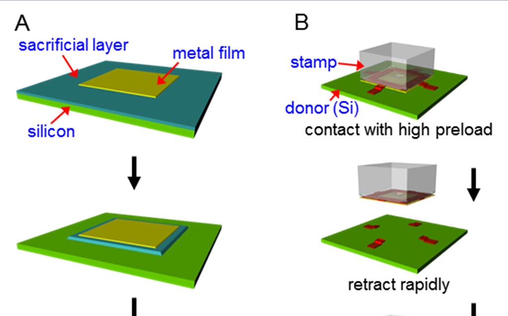
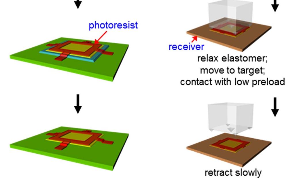
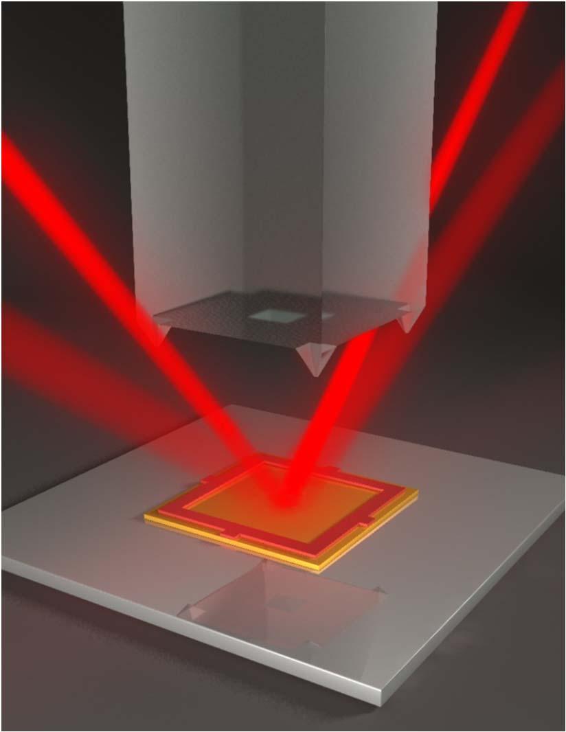
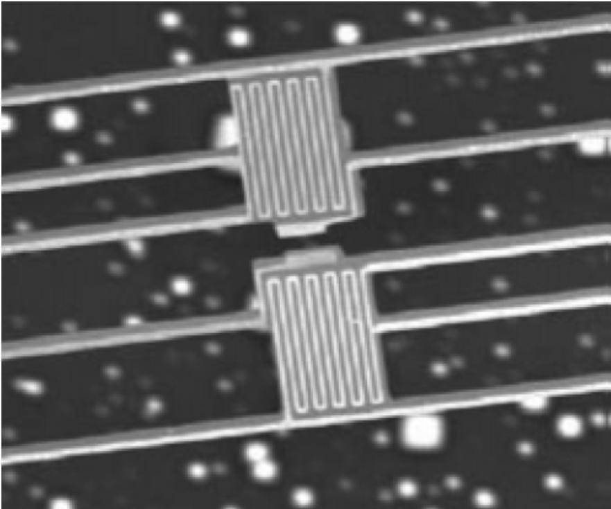
12 Assemble interfaces by transfer-printing
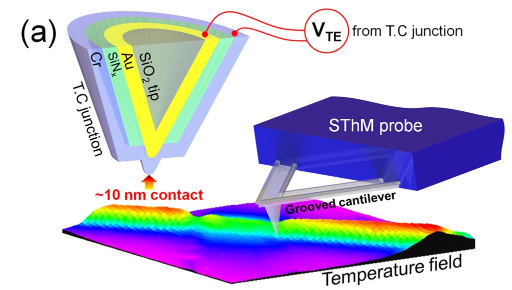
 (a) near-field")
 conduction across true area")
13 Possible mechanisms for heat transfer at an interface between two elastically stiff solids (Persson 2010) (a) near-field electromagnetic radiation (b) gas conduction (c) conduction through H 2 O liquid bridges (d) conduction across true area of contact
Thermal conductance of weak and strong interfaces
 Thermal conductance of weak and strong interfaces David G. Cahill, Wen-Pin Hsieh, Mark Losego, Paul Braun, Dong-Wook Oh, Seok Kim, Eric Pop, Sanjiv Sinha, Paul Braun, and John Rogers Department of Materials
Comparison of the 3ω method and time-domain
 Comparison of the 3ω method and time-domain thermoreflectance David G. Cahill, Shawn Putnam, Yee Kan Koh Materials Research Lab and Department of Materials Science and Engineering, U. of Illinois, Urbana,
Electronic thermal transport in nanoscale metal layers
 Electronic thermal transport in nanoscale metal layers David Cahill, Richard Wilson, Wei Wang, Joseph Feser Department of Materials Science and Engineering Materials Research Laboratory University of Illinois
Ultralow thermal conductivity and the thermal conductance of interfaces
 Ultralow thermal conductivity and the thermal conductance of interfaces David G. Cahill, C. Chiritescu, Y.-K. Koh, X. Zheng, W.-P. Hsieh Materials Research Lab and Department of Materials Science, U. of
extremes of heat conduction: Pushing the boundaries of the thermal conductivity of materials
 extremes of heat conduction: Pushing the boundaries of the thermal conductivity of materials David G. Cahill C. Chiritescu, W.-P. Hsieh, B. Chen, D. Li, G. Hohensee Department of Materials Science and
Olivier Bourgeois Institut Néel
 Olivier Bourgeois Institut Néel Outline Introduction: necessary concepts: phonons in low dimension, characteristic length Part 1: Transport and heat storage via phonons Specific heat and kinetic equation
Nanoscale Surface Physics PHY 5XXX
 SYLLABUS Nanoscale Surface Physics PHY 5XXX Spring Semester, 2006 Instructor: Dr. Beatriz Roldán-Cuenya Time: Tuesday and Thursday 4:00 to 5:45 pm Location: Theory: MAP 306, Laboratory: MAP 148 Office
Nanoscale thermal transport and the thermal conductance of interfaces
 Nanoscale thermal transport and the thermal conductance of interfaces David G. Cahill Scott Huxtable, Zhenbin Ge, Paul Bruan Materials Research Laboratory and Department of Materials Science Zhaohui Wang,
9.3. Total number of phonon modes, total energy and heat capacity
 Phys50.nb 6 E = n = n = exp - (9.9) 9... History of the Planck distribution or the Bose-Einstein distribution. his distribution was firstly discovered by Planck in the study of black-body radiation. here,
Fabrication at the nanoscale for nanophotonics
 Fabrication at the nanoscale for nanophotonics Ilya Sychugov, KTH Materials Physics, Kista silicon nanocrystal by electron beam induced deposition lithography Outline of basic nanofabrication methods Devices
NANOSCIENCE: TECHNOLOGY AND ADVANCED MATERIALS
 UNIVERSITY OF SOUTHAMPTON PHYS6014W1 SEMESTER 2 EXAMINATIONS 2012-2013 NANOSCIENCE: TECHNOLOGY AND ADVANCED MATERIALS DURATION 120 MINS (2 Hours) This paper contains 8 questions Answer ALL questions in
Nanotechnology Fabrication Methods.
 Nanotechnology Fabrication Methods. 10 / 05 / 2016 1 Summary: 1.Introduction to Nanotechnology:...3 2.Nanotechnology Fabrication Methods:...5 2.1.Top-down Methods:...7 2.2.Bottom-up Methods:...16 3.Conclusions:...19
Time-resolved magneto-optical Kerr effect for studies of phonon thermal transport
 Time-resolved magneto-optical Kerr effect for studies of phonon thermal transport David G. Cahill, Jun Liu, Judith Kimling, Johannes Kimling, Department of Materials Science and Engineering University
Outline Scanning Probe Microscope (SPM)
") AFM Outline Scanning Probe Microscope (SPM) A family of microscopy forms where a sharp probe is scanned across a surface and some tip/sample interactions are monitored Scanning Tunneling Microscopy (STM)
AFM Outline Scanning Probe Microscope (SPM) A family of microscopy forms where a sharp probe is scanned across a surface and some tip/sample interactions are monitored Scanning Tunneling Microscopy (STM)
Coupling of heat and spin currents at the nanoscale in cuprates and metallic multilayers
 Coupling of heat and spin currents at the nanoscale in cuprates and metallic multilayers David G. Cahill, Greg Hohensee, and Gyung-Min Choi Department of Materials Science and Engineering University of
High-resolution Characterization of Organic Ultrathin Films Using Atomic Force Microscopy
 High-resolution Characterization of Organic Ultrathin Films Using Atomic Force Microscopy Jing-jiang Yu Nanotechnology Measurements Division Agilent Technologies, Inc. Atomic Force Microscopy High-Resolution
Subject Index. See https://pubs.acs.org/sharingguidelines for options on how to legitimately share published articles.
 Subject Index Downloaded via 148.251.232.83 on July 22, 2018 at 01:11:58 (UTC). See https://pubs.acs.org/sharingguidelines for options on how to legitimately share published articles. A American Chemical
Plasmonic sensing of heat transport and phase change near solid-liquid interfaces
 Plasmonic sensing of heat transport and phase change near solid-liquid interfaces David G. Cahill and Jonglo Park Department of Materials Science and Engineering University of Illinois at Urbana-Champaign
ETH Rüschlikon the people and their research
 ETH Zurich @ Rüschlikon the people and their research Prof. Dr. Dimos Poulikakos, Laboratory of Thermodynamics in Emerging Technologies and Coordinator of the Nanotechnology Center, ETH Zurich The Vision
Scanning Probe Microscopy. Amanda MacMillan, Emmy Gebremichael, & John Shamblin Chem 243: Instrumental Analysis Dr. Robert Corn March 10, 2010
 Scanning Probe Microscopy Amanda MacMillan, Emmy Gebremichael, & John Shamblin Chem 243: Instrumental Analysis Dr. Robert Corn March 10, 2010 Scanning Probe Microscopy High-Resolution Surface Analysis
OPTICAL PROPERTIES AND SPECTROSCOPY OF NANOAAATERIALS. Jin Zhong Zhang. World Scientific TECHNISCHE INFORMATIONSBIBLIOTHEK
 OPTICAL PROPERTIES AND SPECTROSCOPY OF NANOAAATERIALS Jin Zhong Zhang University of California, Santa Cruz, USA TECHNISCHE INFORMATIONSBIBLIOTHEK Y World Scientific NEW JERSEY. t'on.don SINGAPORE «'BEIJING
CSCI 2570 Introduction to Nanocomputing
 CSCI 2570 Introduction to Nanocomputing The Emergence of Nanotechnology John E Savage Purpose of the Course The end of Moore s Law is in sight. Researchers are now exploring replacements for standard methods
Report on 7th US-Japan Joint Seminar on Nanoscale Transport Phenomena Science and Engineering
 Report on 7th US-Japan Joint Seminar on Nanoscale Transport Phenomena Science and Engineering December 11-14, 2011, Shima, Japan co-chairs: Shigeo Maruyama, Kazuyoshi Fushinobu, Jennifer Lukes, Li Shi
master thesis STM studies of molecules for molecular electronics
 STM studies of molecules for molecular electronics Experimental study of single organic molecules by Scanning Tunneling Microscope (STM) and spectroscopy at low temperature Experimental STM images of Aza-BODIPY
Nanostructure. Materials Growth Characterization Fabrication. More see Waser, chapter 2
 Nanostructure Materials Growth Characterization Fabrication More see Waser, chapter 2 Materials growth - deposition deposition gas solid Physical Vapor Deposition Chemical Vapor Deposition Physical Vapor
Outlook. U.S. Army Research Office. 18 May 2017
 UNCLASSIFIED Outlook U.S. Army Research Office 18 May 2017 Dr. David M. Stepp Director, Engineering Sciences Division Chief, Materials Science U.S. Army Research Office david.m.stepp.civ@mail.mil 919-549-4329
Seminars in Nanosystems - I
 Seminars in Nanosystems - I Winter Semester 2011/2012 Dr. Emanuela Margapoti Emanuela.Margapoti@wsi.tum.de Dr. Gregor Koblmüller Gregor.Koblmueller@wsi.tum.de Seminar Room at ZNN 1 floor Topics of the
REFLECTIONS ON THE PAST, PRESENT AND FUTURE OF CONDENSED MATTER PHYSICS. A. J. Leggett
 REFLECTIONS ON THE PAST, PRESENT AND FUTURE OF CONDENSED MATTER PHYSICS A. J. Leggett Department of Physics University of Illinois at Urbana-Champaign American Physical Society March Meeting March 2016
Title Single Row Nano-Tribological Printing: A novel additive manufacturing method for nanostructures
 Nano-Tribological Printing: A novel additive manufacturing method for nanostructures H.S. Khare, N.N. Gosvami, I. Lahouij, R.W. Carpick hkhare@seas.upenn.edu carpick@seas.upenn.edu carpick.seas.upenn.edu
Phonon II Thermal Properties
 Phonon II Thermal Properties Physics, UCF OUTLINES Phonon heat capacity Planck distribution Normal mode enumeration Density of states in one dimension Density of states in three dimension Debye Model for
Picosecond spin caloritronics
 Picosecond spin caloritronics David Cahill, Johannes Kimling, and Gyung-Min Choi Department of Materials Science and Engineering, Materials Research Laboratory, University of Illinois at Urbana-Champaign
Growth of Graphene Architectures on SiC
 Wright State University CORE Scholar Special Session 5: Carbon and Oxide Based Nanostructured Materials (2012) Special Session 5 6-2012 Growth of Graphene Architectures on SiC John J. Boeckl Weijie Lu
Institute of Materials Science of Mulhouse. Vincent Roucoules. UMR 7361 CNRS. 27 th november, 2017 SULZBACH- ROSEMBERG (GERMANY)
") Institute of Materials Science of Mulhouse Director(s): Mulhouse Cathie Vix Vincent Roucoules UMR 7361 CNRS www.is2m.uha.fr 10,0 µ 27 th november, 2017 SULZBACH- ROSEMBERG (GERMANY) Institute of Materials
Institute of Materials Science of Mulhouse Director(s): Mulhouse Cathie Vix Vincent Roucoules UMR 7361 CNRS www.is2m.uha.fr 10,0 µ 27 th november, 2017 SULZBACH- ROSEMBERG (GERMANY) Institute of Materials
Welcome to NANO* 2000
 Lecture Zero Welcome to NANO* 2000 First - the "big picture" of the course and the course outline -grading scheme - exam schedule - review paper - lab (Jay) last revision September 4 2013: MDB 0-1 NANO*
Explain how Planck resolved the ultraviolet catastrophe in blackbody radiation. Calculate energy of quanta using Planck s equation.
 Objectives Explain how Planck resolved the ultraviolet catastrophe in blackbody radiation. Calculate energy of quanta using Planck s equation. Solve problems involving maximum kinetic energy, work function,
CHAPTER 7 ELECTRODYNAMICS
 CHAPTER 7 ELECTRODYNAMICS Outlines 1. Electromotive Force 2. Electromagnetic Induction 3. Maxwell s Equations Michael Faraday James C. Maxwell 2 Summary of Electrostatics and Magnetostatics ρ/ε This semester,
Time and space resolved spectroscopy of nanoenergetic materials Dana Dlott
 Time and space resolved spectroscopy of nanoenergetic materials Dana Dlott Hyunung Yu Selezion A. Hambir School of Chemical Sciences and Fredrick Seitz Materials Research Laboratory University of Illinois
Scanning Tunneling Microscopy. how does STM work? the quantum mechanical picture example of images how can we understand what we see?
 Scanning Tunneling Microscopy how does STM work? the quantum mechanical picture example of images how can we understand what we see? Observation of adatom diffusion with a field ion microscope Scanning
Supporting Information
 Supporting Information Assembly and Densification of Nanowire Arrays via Shrinkage Jaehoon Bang, Jonghyun Choi, Fan Xia, Sun Sang Kwon, Ali Ashraf, Won Il Park, and SungWoo Nam*,, Department of Mechanical
NUS Italian Graphene Centre workshop 2014 : Talks Schedule
 NUS Italian Graphene Centre workshop 2014 : Talks Schedule Time Monday, March 17 Tuesday, March 18 8:30 9:00 Opening by Prof Antonio Castro Neto (NUS) 9:00 9:45 Prof Vittorio Pellegrini (ITT) Prof Antonio
Introduction to Scanning Probe Microscopy Zhe Fei
 Introduction to Scanning Probe Microscopy Zhe Fei Phys 590B, Apr. 2019 1 Outline Part 1 SPM Overview Part 2 Scanning tunneling microscopy Part 3 Atomic force microscopy Part 4 Electric & Magnetic force
Thermally Functional Liquid Crystal Networks by Magnetic Field Driven Molecular Orientation
 Supporting information Thermally Functional Liquid Crystal Networks by Magnetic Field Driven Molecular Orientation Jungwoo Shin, Minjee Kang, Tsunghan Tsai, Cecilia Leal, Paul V. Braun and David G. Cahill*,
Scienza e Tecnologia dei Materiali Ceramici. Modulo 2: Materiali Nanostrutturati
 Università degli Studi di Trieste Dipartimento di Ingegneria e Architettura A.A. 2016-2017 Scienza e Tecnologia dei Materiali Ceramici Modulo 2: Materiali Nanostrutturati - Lezione 5 - Vanni Lughi vlughi@units.it
There s plenty of room at the bottom! - R.P. Feynman, Nanostructure: a piece of material with at least one dimension less than 100 nm in extent.
 Nanostructures and Nanotechnology There s plenty of room at the bottom! - R.P. Feynman, 1959 Materials behave differently when structured at the nm scale than they do in bulk. Technologies now exist that
Self-assembled nanostructures for antireflection optical coatings
 Self-assembled nanostructures for antireflection optical coatings Yang Zhao 1, Guangzhao Mao 2, and Jinsong Wang 1 1. Deaprtment of Electrical and Computer Engineering 2. Departmentof Chemical Engineering
Nanoparticle Devices. S. A. Campbell, ECE C. B. Carter, CEMS H. Jacobs, ECE J. Kakalios, Phys. U. Kortshagen, ME. Institute of Technology
 Nanoparticle Devices S. A. Campbell, ECE C. B. Carter, CEMS H. Jacobs, ECE J. Kakalios, Phys. U. Kortshagen, ME Applications of nanoparticles Flash Memory Tiwari et al., Appl. Phys. Lett. 68, 1377, 1996.
Optimization of MnO2 Electrodeposits using Graphenated Carbon Nanotube Electrodes for Supercapacitors
 Optimization of MnO2 Electrodeposits using Graphenated Carbon Nanotube Electrodes for Supercapacitors Waleed Nusrat, 100425398 PHY 3090U Material Science Thursday April 9 th 2015 Researchers optimize the
Contents. Preface to the first edition
 Contents List of authors Preface to the first edition Introduction x xi xiii 1 The nanotechnology revolution 1 1.1 From micro- to nanoelectronics 2 1.2 From the macroscopic to the nanoscopic world 4 1.3
Interdisciplinary Nanoscience Center University of Aarhus, Denmark. Design and Imaging. Assistant Professor.
 Interdisciplinary Nanoscience Center University of Aarhus, Denmark Design and Imaging DNA Nanostructures Assistant Professor Wael Mamdouh wael@inano.dk Molecular Self-assembly Synthesis, SPM microscopy,
2D Materials Research Activities at the NEST lab in Pisa, Italy. Stefan Heun NEST, Istituto Nanoscienze-CNR and Scuola Normale Superiore, Pisa, Italy
 2D Materials Research Activities at the NEST lab in Pisa, Italy Stefan Heun NEST, Istituto Nanoscienze-CNR and Scuola Normale Superiore, Pisa, Italy 2D Materials Research Activities at the NEST lab in
Lecture 3. Self-assembled Monolayers (SAM)
") 10.524 Lecture 3. Self-assembled Monolayers (SAM) Instructor: Prof. Zhiyong Gu (Chemical Engineering & UML CHN/NCOE Nanomanufacturing Center) Lecture 3: Self-assembled Monolayers (SAMs) Table of Contents
10.524 Lecture 3. Self-assembled Monolayers (SAM) Instructor: Prof. Zhiyong Gu (Chemical Engineering & UML CHN/NCOE Nanomanufacturing Center) Lecture 3: Self-assembled Monolayers (SAMs) Table of Contents
From nanophysics research labs to cell phones. Dr. András Halbritter Department of Physics associate professor
 From nanophysics research labs to cell phones Dr. András Halbritter Department of Physics associate professor Curriculum Vitae Birth: 1976. High-school graduation: 1994. Master degree: 1999. PhD: 2003.
April 13, 2011 Exam 4, Friday. Review sheet posted. Sky Watch 4 due. Review session Thursday, 5 6 PM, Room WEL 3.502, right here! Reading: Chapter 9,
 April 13, 2011 Exam 4, Friday. Review sheet posted. Sky Watch 4 due. Review session Thursday, 5 6 PM, Room WEL 3.502, right here! Reading: Chapter 9, Sections 9.5.2, 9.6.1, 9.6.2. 9.7, 9.8; Chapter 10,
Nanotechnology where size matters
 Nanotechnology where size matters J Emyr Macdonald Overview Ways of seeing very small things What is nanotechnology and why is it important? Building nanostructures What we can do with nanotechnology?
Lecture Outline Chapter 30. Physics, 4 th Edition James S. Walker. Copyright 2010 Pearson Education, Inc.
 Lecture Outline Chapter 30 Physics, 4 th Edition James S. Walker Chapter 30 Quantum Physics Units of Chapter 30 Blackbody Radiation and Planck s Hypothesis of Quantized Energy Photons and the Photoelectric
Ultrafast laser-based metrology for micron-scale measurements of thermal transport, coefficient of thermal expansion, and temperature
 Ultrafast laser-based metrology for micron-scale measurements of thermal transport, coefficient of thermal expansion, and temperature David G. Cahill, Xuan Zheng, Chang-Ki Min, Ji-Yong Park Materials Research
Morphological evolution of single-crystal ultrathin solid films
 Western Kentucky University From the SelectedWorks of Mikhail Khenner March 29, 2010 Morphological evolution of single-crystal ultrathin solid films Mikhail Khenner, Western Kentucky University Available
Surface Science (Chemistry)
") Surface Science Mankind has studied surface and interface phenomena since antiquity. In old Babylon a form of divination, called lecanomancy, involved an examination of the properties of oil poured into
Surface Science Mankind has studied surface and interface phenomena since antiquity. In old Babylon a form of divination, called lecanomancy, involved an examination of the properties of oil poured into
Instrumentation and Operation
 Instrumentation and Operation 1 STM Instrumentation COMPONENTS sharp metal tip scanning system and control electronics feedback electronics (keeps tunneling current constant) image processing system data
 http://www.physics.ucdavis.edu/condensed_matter.html A brief introduction to Condensed Matter Physics at Davis and an overview of the Condensed Matter Experiment Group The Past-- 30 Years of Nobel Prizes
Current and Emergent Developments
 Self Assembly and Biologically Inspired Processes in Applied Nanotechnology: Current and Emergent Developments Charles Ostman VP, Electronics & Photonics Forum chair NanoSig Senior Consultant Silicon Valley
Nanobiotechnology. Place: IOP 1 st Meeting Room Time: 9:30-12:00. Reference: Review Papers. Grade: 40% midterm, 60% final report (oral + written)
") Nanobiotechnology Place: IOP 1 st Meeting Room Time: 9:30-12:00 Reference: Review Papers Grade: 40% midterm, 60% final report (oral + written) Midterm: 5/18 Oral Presentation 1. 20 minutes each person
Nanobiotechnology Place: IOP 1 st Meeting Room Time: 9:30-12:00 Reference: Review Papers Grade: 40% midterm, 60% final report (oral + written) Midterm: 5/18 Oral Presentation 1. 20 minutes each person
Research Grants Approved and Funded
 Research Grants Approved and Funded Koratkar has won 35 grants (totaling ~ $9.7 Million) from several agencies such as the National Science Foundation, Office of Naval Research, Army Research Office, Advanced
Physics Open House Boston University Physics Department
 2012 Boston University Physics Department What are the Big Questions? Dept. of Energy BESAC Report (2007): Directing Boston UniversityMatter Slideshow Title and Goes Energy: Here Five Challenges for Science
Scalable Nanomaterials and Nanostructures for Energy and Flexible Electronics
 Scalable Nanomaterials and Nanostructures for Energy and Flexible Electronics Liangbing (Bing) Hu MSE & Energy Center University of Maryland College Park Email: binghu@umd.edu 1 Transparent Paper from
what happens if we make materials smaller?
 what happens if we make materials smaller? IAP VI/10 ummer chool 2007 Couvin Prof. ns outline Introduction making materials smaller? ynthesis how do you make nanomaterials? Properties why would you make
Pure Science; The Pursuit of Things With No Foreseeable Benefit. By Cory Cluff
 Pure Science; The Pursuit of Things With No Foreseeable Benefit. By Cory Cluff In American history many madmen have carried out wasteful schemes of great scope in the name of science. They have frittered
Chapter 1 Introduction
 Chapter 1 Introduction A nanometer (nm) is one billionth (10-9 ) of a meter. Nanoscience can be defined as the science of objects and phenomena occurring at the scale of 1 to 100 nm. The range of 1 100
Déposition séléctive le rêve reviens
 Willkommen Welcome Bienvenue Déposition séléctive le rêve reviens Patrik Hoffmann Michael Reinke, Yury Kuzminykh Ivo Utke, Carlos Guerra-Nunez, Ali Dabirian, Xavier Multone, Tristan Bret, Estelle Halary-Wagner,
2015 Summer School on Emergent Phenomena in Quantum Materials. Program Overview
 Emergent Phenomena in Quantum Materials Program Overview Each talk to be 45min with 15min Q&A. Monday 8/3 8:00AM Registration & Breakfast 9:00-9:10 Welcoming Remarks 9:10-10:10 Eugene Demler Harvard University
Material Analysis. What do you want to know about your sample? How do you intend to do for obtaining the desired information from your sample?
 Material Analysis What do you want to know about your sample? How do you intend to do for obtaining the desired information from your sample? Why can you acquire the proper information? Symmetrical stretching
 For info and ordering all the 4 versions / languages of this book please visit: http://trl.lab.uic.edu/pon Contents Preface vii Chapter 1 Advances in Atomic and Molecular Nanotechnology Introduction 1
Modeling and Computation Core (MCC)
") List of Research by Research Cluster Modeling and Computation Core (MCC) GOAL 1: Develop multiscale theories and materials databank that complement experimental approaches for materials design Objective
List of Research by Research Cluster Modeling and Computation Core (MCC) GOAL 1: Develop multiscale theories and materials databank that complement experimental approaches for materials design Objective
Fabrication of ordered array at a nanoscopic level: context
 Fabrication of ordered array at a nanoscopic level: context Top-down method Bottom-up method Classical lithography techniques Fast processes Size limitations it ti E-beam techniques Small sizes Slow processes
UV-vis Analysis of the Effect of Sodium Citrate on the Size and the Surface Plasmon Resonance of Au NPs. Eman Mousa Alhajji
 UV-vis Analysis of the Effect of Sodium Citrate on the Size and the Surface Plasmon Resonance of Au NPs Eman Mousa Alhajji North Carolina State University Department of Materials Science and Engineering
Supporting Information for
 Supporting Information for Enhancing the Thermal Conductance of Polymer and Sapphire Interface via Self-Assembled Monolayer Kun Zheng,,+ Fangyuan Sun,,+ Jie Zhu, *,, Yongmei Ma, *, Xiaobo Li, Dawei Tang,
Reviewers' comments: Reviewer #1 (Remarks to the Author):
:") Reviewers' comments: Reviewer #1 (Remarks to the Author): The work is very interesting as it presents a way to reduce the ohmic losses in the metals in the finite range of frequencies. In this the work
Reviewers' comments: Reviewer #1 (Remarks to the Author): The work is very interesting as it presents a way to reduce the ohmic losses in the metals in the finite range of frequencies. In this the work
Transport through Andreev Bound States in a Superconductor-Quantum Dot-Graphene System
 Transport through Andreev Bound States in a Superconductor-Quantum Dot-Graphene System Nadya Mason Travis Dirk, Yung-Fu Chen, Cesar Chialvo Taylor Hughes, Siddhartha Lal, Bruno Uchoa Paul Goldbart University
Micro Chemical Vapor Deposition System: Design and Verification
 Micro Chemical Vapor Deposition System: Design and Verification Q. Zhou and L. Lin Berkeley Sensor and Actuator Center, Department of Mechanical Engineering, University of California, Berkeley 2009 IEEE
Institute for Functional Imaging of Materials (IFIM)
") Institute for Functional Imaging of Materials (IFIM) Sergei V. Kalinin Guiding the design of materials tailored for functionality Dynamic matter: information dimension Static matter Functional matter Imaging
Institute for Functional Imaging of Materials (IFIM) Sergei V. Kalinin Guiding the design of materials tailored for functionality Dynamic matter: information dimension Static matter Functional matter Imaging
QS School Summary
 2018 NSF/DOE/AFOSR Quantum Science Summer School June 22, 2018 QS 3 2018 School Summary Kyle Shen (Cornell) Some Thank yous! A Big Thanks to Caroline Brockner!!! Also to our fantastic speakers! Kavli Institute
City University of Hong Kong. Course Syllabus. offered by Department of Physics and Materials Science with effect from Semester A 2016 / 17
 City University of Hong Kong offered by Department of Physics and Materials Science with effect from Semester A 2016 / 17 Part I Course Overview Course Title: Nanostructures and Nanotechnology Course Code:
Nanoscale Energy Transport and Conversion A Parallel Treatment of Electrons, Molecules, Phonons, and Photons
 Nanoscale Energy Transport and Conversion A Parallel Treatment of Electrons, Molecules, Phonons, and Photons Gang Chen Massachusetts Institute of Technology OXFORD UNIVERSITY PRESS 2005 Contents Foreword,
ESS 5855 Surface Engineering for. MicroElectroMechanicalechanical Systems. Fall 2010
 ESS 5855 Surface Engineering for Microelectromechanical Systems Fall 2010 MicroElectroMechanicalechanical Systems Miniaturized systems with integrated electrical and mechanical components for actuation
Bandgap engineering through nanocrystalline magnetic alloy grafting on. graphene
 Electronic Supplementary Material (ESI) for Physical Chemistry Chemical Physics. This journal is the Owner Societies 2014 Electronic Supplementary Information (ESI) for Bandgap engineering through nanocrystalline
What is the role of simulation in nanoscience research?
 ChE/MSE 557 Intro part 2 What is the role of simulation in nanoscience research? 1 Opportunities for Simulation Simulation Simulation complements both experiment and theory. Extends window of observation
Hawking & the Universe
 Hawking & the Universe This is a supplement to the lecture given on Jan 26, 2015, by Dr. Mounib El Eid, Physics department, AUB. It may motivate the reader to explore some of the presented issues. There
TEACHING MICRO/NANOSCALE HEAT TRANSFER
 56 Purdue Heat Transfer Celebration April 3-5, 2002, West Lafayette, IN TEACHING MICRO/NANOSCALE HEAT TRANSFER Gang Chen Mechanical Engineering Department Massachusetts Institute of Technology Cambridge,
Doctor of Philosophy
 FEMTOSECOND TIME-DOMAIN SPECTROSCOPY AND NONLINEAR OPTICAL PROPERTIES OF IRON-PNICTIDE SUPERCONDUCTORS AND NANOSYSTEMS A Thesis Submitted for the degree of Doctor of Philosophy IN THE FACULTY OF SCIENCE
Lecture 30: Kinetics of Epitaxial Growth: Surface Diffusion and
 Lecture 30: Kinetics of Epitaxial Growth: Surface Diffusion and Nucleation Today s topics Understanding the basics of epitaxial techniques used for surface growth of crystalline structures (films, or layers).
Impact of disorder and topology in two dimensional systems at low carrier densities
 Impact of disorder and topology in two dimensional systems at low carrier densities A Thesis Submitted For the Degree of Doctor of Philosophy in the Faculty of Science by Mohammed Ali Aamir Department
May the Force be with you: High-speed Atomic Force Microscopes for Synchrotron Sample Holders Luca Costa
 May the Force be with you: High-speed Atomic Force Microscopes for Synchrotron Sample Holders Luca Costa ESRF, The European Synchrotron 71 Rue des Martyrs, 38000 Grenoble, France EXP DIV - THE SURFACE
Thermal characterization of Au-Si multilayer using 3- omega method
 Thermal characterization of Au-Si multilayer using 3- omega method Sunmi Shin Materials Science and Engineering Program Abstract As thermal management becomes a serious issue in applications of thermoelectrics,
Supplementary Information for Solution-Synthesized Chevron Graphene Nanoribbons Exfoliated onto H:Si(100)
") Supplementary Information for Solution-Synthesized Chevron Graphene Nanoribbons Exfoliated onto H:Si(100) Adrian Radocea,, Tao Sun,, Timothy H. Vo, Alexander Sinitskii,,# Narayana R. Aluru,, and Joseph
Supplementary Information for Solution-Synthesized Chevron Graphene Nanoribbons Exfoliated onto H:Si(100) Adrian Radocea,, Tao Sun,, Timothy H. Vo, Alexander Sinitskii,,# Narayana R. Aluru,, and Joseph
ARFTG 84th WORKSHOP The New Frontiers for Microwave Measurements
 84th ARFTG Microwave Measurement Conference ARFTG 84th WORKSHOP The New Frontiers for Microwave Measurements December 3rd, 2014 Boulder, Colorado St. Julien Hotel 84 th ARFTG Topic: The New Frontiers for
Techniques useful in biodegradation tracking and biodegradable polymers characterization
 Techniques useful in biodegradation tracking and biodegradable polymers characterization Version 1 Wanda Sikorska and Henryk Janeczek 1 Knowledge on biodegradable polymers structures is essential for the
Thermal Transport in Graphene and other Two-Dimensional Systems. Li Shi. Department of Mechanical Engineering & Texas Materials Institute
 Thermal Transport in Graphene and other Two-Dimensional Systems Li Shi Department of Mechanical Engineering & Texas Materials Institute Outline Thermal Transport Theories and Simulations of Graphene Raman
The Dielectric Function of a Metal ( Jellium )
") The Dielectric Function of a Metal ( Jellium ) Total reflection Plasma frequency p (10 15 Hz range) Why are Metals Shiny? An electric field cannot exist inside a metal, because metal electrons follow the
The Dielectric Function of a Metal ( Jellium ) Total reflection Plasma frequency p (10 15 Hz range) Why are Metals Shiny? An electric field cannot exist inside a metal, because metal electrons follow the
[ ( )] + exp 2α / ( k B T) [ ] + exp 3α / k B T
![[ ( )] + exp 2α / ( k B T) [ ] + exp 3α / k B T](/thumbs/81/84416061.jpg "[ ( )] + exp 2α / ( k B T) [ ] + exp 3α / k B T") hermal Physics Homework #10 (optional) (19 points) 1 Your work on this homework set will not be accepted after 3 p.m. on December 4 (W) 1. (3 points) A common mistake people make when they try to calculate
hermal Physics Homework #10 (optional) (19 points) 1 Your work on this homework set will not be accepted after 3 p.m. on December 4 (W) 1. (3 points) A common mistake people make when they try to calculate
Notes: Pythagorean Triples
 Math 5330 Spring 2018 Notes: Pythagorean Triples Many people know that 3 2 + 4 2 = 5 2. Less commonly known are 5 2 + 12 2 = 13 2 and 7 2 + 24 2 = 25 2. Such a set of integers is called a Pythagorean Triple.