Mobility enhancement and highly efficient gating of monolayer MoS 2 transistors with Polymer Electrolyte
|
|
|
- Noreen Powers
- 5 years ago
- Views:
Transcription
1 Mobility enhancement and highly efficient gating of monolayer MoS 2 transistors with Polymer Electrolyte Ming-Wei Lin 1, Lezhang Liu 1, Qing Lan 1, Xuebin Tan 2, Kulwinder Dhindsa 1, Peng Zeng 2, Vaman M. Naik 3, Mark Ming-Cheng Cheng 2 1, a), and Zhixian Zhou 1 Department of Physics and Astronomy, Wayne State University, Detroit, MI Department of Electrical and Computer Engineering, Wayne State University, Detroit, MI Department of Natural Sciences, University of Michigan-Dearborn Dearborn, MI Abstract We report electrical characterization of monolayer molybdenum disulfide (MoS 2 ) devices using a thin layer of polymer electrolyte consisting of poly(ethylene oxide) (PEO) and lithium perchlorate (LiClO 4 ) as both a contact-barrier reducer and channel mobility booster. We find that bare MoS 2 devices (without polymer electrolyte) fabricated on Si/SiO 2 have low channel mobility and large contact resistance, both of which severely limit the field-effect mobility of the devices. A thin layer of PEO/ LiClO 4 deposited on top of the devices not only substantially reduces the contact resistance but also boost the channel mobility, leading up to three-orders-ofmagnitude enhancement of the field-effect mobility of the device. When the polymer electrolyte is used as a gate medium, the MoS 2 field-effect transistors exhibit excellent device characteristics such as a near ideal subthreshold swing and an on/off ratio of 10 6 as a result of the strong gatechannel coupling. a) Author to whom correspondence should be addressed, electronic mail: zxzhou@wayne.edu 1
2 1. Introduction Graphene has opened the tantalizing possibility of post-silicon high performance electronics because of its one atomic-layer thickness and extraordinarily high carrier mobility [1-4]. However, the lack of an appreciable bandgap in graphene poses a major problem for conventional digital applications. As a semiconducting analogue of graphene, single-layer MoS 2 has a direct bandgap of ~1.8 ev, which makes it a suitable channel material for low power digital electronics.[5] Similar to graphene, atomic layers of covalently bonded S-Mo-S unites can be extracted from bulk MoS 2 crystals by a mechanical cleavage technique due to relatively weak van der Waals interactions between the layers. However, the carrier mobility in monolayer and few-layer MoS 2 field-effect transistors (FETs) fabricated on Si/SiO 2 substrates are typically in the range of cm 2 V -1 s -1, which is not only orders of magnitude lower than that of graphene but also substantially lower than the phonon-scattering-limited mobility in bulk MoS 2 (which is on the order of 100 cm 2 V -1 s -1 ). [6-9] Radisavljevic et al. have recently shown that the mobility of monolayer MoS 2 FETs can be improved to at least 200 cm 2 V -1 s -1 by depositing a thin layer of HfO 2 high-κ gate dielectric on top of MoS 2 devices, where the significant mobility enhancement was attributed to the suppression of Coulomb scattering due to the high-κ environment and modification of phonon dispersion.[10] However, it is not clear to what extent the observed mobility increase can be attributed to the screening of charged impurities and phonon dispersion modification. On the one hand, a temperature-dependent electrical transport study of monolayer and few-layer MoS 2 FETs by Ghatak et al. suggests that the relatively low mobility in MoS 2 FET devices fabricated on Si/SiO 2 substrate is a channel effect, largely limited by the chargeimpurity-induced electron localization.[7] On the other hand, Lee et al. showed that the 2
3 mobility in MoS 2 FETs fabricated on Si/SiO 2 substrate can be largely underestimated due to the Schottky barriers at the MoS 2 /metal contacts.[11] In this article, we report a simple method to fabricate high mobility (~10 2 cm 2 V -1 s -1 ) MoS 2 FETs by covering the devices with a thin layer of polymer electrolyte (PE) consisting of poly(ethylene oxide) (PEO) and lithium perchlorate (LiClO 4 ). The estimated room-temperature field-effect mobility of the monolayer MoS 2 FETs increases by up to three orders of magnitude upon adding the PE. To study the respective influence of the MoS 2 /metal contacts and MoS 2 channel on the device characteristics, we fabricated multiple devices with different channel lengths on a single ribbon of monolayer MoS 2 with uniform width. Electrical characterization of these devices reveals that the PE-induced mobility enhancement can be attributed partially to the drastic reduction of contact resistance and partially to the increase of the channel mobility. The improvement of the channel mobility is likely due to the neutralization of the uncorrelated charged impurities on or near the MoS 2 channel by the counter ions in the PE.[12-14] Furthermore, we demonstrate for the first time that near ideal gate-channel coupling can be achieved in our PE gated MoS 2 FETs with the subthreshold swing approaching the theoretical limit of 60 mv dec -1 at room temperature for metal oxide semiconductor field-effect transistors (MOSFETs). 2. Experimental Details Monolayer MoS 2 flakes were produced by repeated splitting of MoS 2 crystals by a mechanical cleavage method, and subsequently transferred to degenerately doped silicon substrates covered with a 290 nm-thick thermal oxide layer.[6, 15] An optical microscope was used to identify monolayer (and few-layer) MoS 2 samples, which were further characterized by non-contact 3
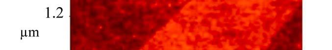
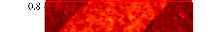
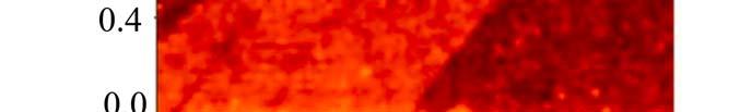
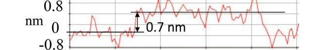
4 mode atomic force microscopy (AFM) and Raman spectroscopy. Figure 1a shows an atomic force microscopy (AFM) image of a typical monolayer MoS 2. From a line scan of the AFM image (figure 1b), we estimate that the MoS 2 sample is ~ 0.7 nm thick, corresponding to a single layer.[8, 10] Raman Spectra were collected using a Jobin Yvon Horiba Triax 550 spectrometer, a liquid-nitrogen cooled charge-coupled device (CCD) detector, an Olympus model BX41 microscope with a 100 objective, and a Modu-Laser (Stellar-Pro-L) Argon-ion laser operating at nm. The laser spot size was ~ 1 µm in diameter and the laser power at the sample was maintained at low level (~ 200 µw) to avoid any heating effect. The Raman spectrum of the sample shows two peaks at cm -1 and 403 cm -1 (figure 1c), which can be associated with the in-plane E 1 2g and out-of-plane A 1g vibrations of a monolayer MoS 2, respectively.[16] FET devices of monolayer MoS 2 were fabricated using standard electron beam lithography and electron beam deposition of 5 nm of Ti and 50 nm of Au.[17] A PE was prepared in air by dissolving PEO and LiClO 4 in the 8:1 weight ratio in de-ionized water, and then drop casted onto the MoS 2 devices, where the PE gate electrodes were simultaneously patterned on the substrate along with the drain and source electrodes.[18] The PE-electrode was kept very close to the device channel; and the coverage of the PE was also limited to within an area of less than 100 µm around the channel and PE-electrode. Figure 2a shows a micrograph of a typical MoS 2 device with schematically illustrated PE. Electrical properties of the devices were measured by a Keithley 4200 semiconductor parameter analyzer in vacuum (~ Torr) and at room temperature (unless otherwise specified) both before and after adding the PE. The electrical measurements were conducted in both the Si back gate (with or without PE) and PEgate configurations. As schematically shown in figure 4a, when a positive (negative) voltage is applied to a PE-gate-electrode near the device channel, negative(positive) and positive (negative) 4
5 ions in the PE accumulate on the gate electrode and channel, respectively, forming electric double layers (EDL) at their interfaces with the electrolyte.[19] 3. Results and discussions We first measured the electrical properties of several monolayer MoS 2 FET devices without PE and found a consistently low mobility between 0.1 and 1.5 cm 2 V -1 S -1, which is in agreement with the values reported in the literature.[6, 7, 20] Upon adding the PE, a significant mobility increase is observed in all devices. Figure 2b shows the low-bias linear conductivity defined as ơ = L/W I ds /V ds versus back gate voltage in a typical monolayer MoS 2 device (device A) before and after adding the PE layer. Here L, W, I ds, and V ds are the channel length (5.9 µm), channel width (0.6 µm), drain-source current, and drain-source voltage, respectively. The field-effect mobility estimated from the linear region of the transfer characteristics of the device using the formula µ= Δơ /(C bg ΔV g ) before and after adding the PE is ~0.1 cm 2 V -1 s -1 and ~ 150 cm 2 V -1 S -1, respectively. Here C bg = F cm -2 is the capacitance between the channel and the back gate per unit area (C bg = Ɛ 0 Ɛ r /d; Ɛ r = 3.9; d = 290 nm). Similar mobility improvement has been observed in monolayer MoS 2 FETs by Radisavljevic et al. upon depositing a thin layer of HfO 2 on top, which was attributed to the suppression of the Coulomb scattering due the high-κ dielectric environment and modification of phonon dispersion in MoS 2 monolayers.[10] However, the dielectric constant of the PE (Ɛ = 5) used in this study is much lower than that of HfO 2.[21] Moreover, the mobility of the devices drops drastically upon cooling below the freezing temperature of the ions in the PE, ruling out dielectric screening as the dominant mechanism responsible for the mobility enhancement in our devices (see figure 3c and detailed discussion below). 5
6 A possible mechanism for the field-effect mobility improvement in our devices is the ionic screening effect. At any given back gate voltage, the free counter ions in the PE accumulate on the graphene surface to neutralize the uncorrelated charged impurities.[12-14] Two orders of magnitude increase of mobility has been previously observed in graphene FETs immersed in ionic solutions, which was attributed to the ionic screening of charged impurity scattering in graphene.[12, 14] Although the PE is expected to introduce additional charged impurities, studies on PE gated carbon nanotube and graphene FETs show that the mobility of these devices remains high (on the order of 10 3 cm 2 V -1 s -1 ) upon adding PEO/LiClO 4 PE. [1, 8, 19, 22] One likely scenario is that the Li + and ClO - 4 ions accumulated on the channel surfaces are correlated in contrast to the uncorrelated initial charged impurities near or on the channel surfaces. Even modest correlations in the position of charged impurities has been shown to substantially increase the mobility in graphene.[23] Therefore, the neutralization of the uncorrelated charged impurities on or near the MoS 2 surface by the counter ions from the PE is likely, at least partially, responsible for the orders of magnitude increase of the mobility upon addition of PE. A second possibility is that the mobility of our MoS 2 devices without PE is substantially underestimated due to the presence of Schottky barriers at the MoS 2 /metal contacts (the contact resistance was not excluded in calculating the mobility). Figure 3a shows the drain-source current ( I ds ) versus bias voltage ( V ds ) measured at different back gate voltages for the same MoS 2 device (device A) before depositing the PE. Although the device exhibits linear and symmetric I ds -V ds dependence at low V ds (figure 3a inset), the I ds -V ds behavior is non-linear and asymmetric at high bias-voltages. When the drain and source electrode connections are physically exchanged, the I ds -V ds characteristics also change suggesting the presence of asymmetry and possibly non-negligible Schottky barriers at the contacts. It has been recently 6
7 reported that the current flow in MoS 2 can be largely limited by the contact barriers leading to a significant underestimate of the mobility.[11] Modeling the I ds -V ds characteristics of individual MoS 2 flakes with proper consideration of the contact barriers yields mobility values comparable to the estimated field-effect mobility in our PE-covered monolayer MoS 2 devices as well as that reported in HfO 2 -covered MoS 2 devices.[10] Liu et al. have further demonstrated that the fieldeffect mobility of multilayer ( ~ 20 monolayers) MoS 2 FETs exceeds 500 cm 2 /V.s due to the smaller bandgap (thus smaller Schottky barrier) compared to monolayer MoS 2.[24] Therefore, a substantial reduction of the contact barriers is also likely to significantly increase the slope of the transfer characteristics (dơ/dv g ), leading to a higher estimated field-effect mobility. To shed more light on the origin of the PE-induced mobility enhancement in our MoS 2 FET devices, it is necessary to investigate the respective contributions of the MoS 2 /metal contacts and the MoS 2 channel to the total resistance of the device at various gate voltages before and after adding the PE. In figure 3b, we plot the resistances of multiple FETs fabricated on the same monolayer MoS 2 ribbon with uniform width as a function of the channel length before adding the PE, where each resistance value is calculated from the slope of the I ds -V ds characteristics in the low- bias linear regime as shown in the inset of figure 3a. It is obvious that the resistance increases nearly linearly with the channel length, from which the contact resistance is estimated to be 40 MΩ and 150 MΩ at V bg = 40 and 30 V, respectively. The scattering of data at V bg = 30 V may be due to the contact resistance variation among different devices. The channel resistance for the device with L = 5.9 µm ( device A ) is several times larger than its contact resistance at all gate voltages, suggesting that the field-effect behavior in our long channel devices is dominated by the channel instead of the contacts. This finding is consistent with that of Radisavljevic et al. [10] Upon applying the PE, the low-bias resistance of the device 7
8 decreases to below 2 MΩ for V bg > 3 V as shown in the figure 3b inset. In the linear region of the transfer characteristics (from which the field-effect mobility is estimated), the total resistance of the device (device A) with PE remains below 7 MΩ, which is significantly lower than either the contact resistance or the channel resistance alone without the PE. This finding shows that covering our single layer MoS 2 FETs with PE not only reduces the channel resistance but also lowers the contact barriers, both of which are critical to improving the field-effect mobility of the MoS 2 FETs. While the improvement of the channel mobility can be attributed to the neutralization of uncorrelated charged impurities, the reduction of the contact barriers could be due to the modification of the metal work function at the contacts by the PE. It has been shown that the adsorption of certain molecules on electrode-metal surfaces can induce a strong decrease in the work function.[25] As our MoS 2 devices are n-type, reducing the work function lowers the Schottky barriers at the contacts. [11] Due to the interplay of the variations in the channel mobility enhancement and contact barrier reduction, the resistance of the devices does not follow the linear dependence on the channel length, making it difficult to accurately extract the contact resistance in MoS 2 devices with PE. Addition of a top dielectric medium has also been shown to increase the back gate capacitance by up to two orders of magnitude in graphene FETs, leading to an overestimation of the mobility when this dramatic capacitance increase was not accounted for.[26, 27] In order to rule out this possibility and further verify that the increase of dơ/dv g upon applying the PE was indeed due to the combined effects of contact resistance reduction and channel mobility increase, we show in Figure 3c the transfer characteristics of another monolayer MoS 2 device (device B) measured below and above the freezing temperature of the Li + and ClO - 4 ions. The nearly two orders of magnitude lower dơ/dv g (which is proportional to the mobility) at 220 K than at 295 K 8
9 is likely due to the freezing of both the Li + and ClO - 4 ions inside the PEO polymer. Thus they are no longer able to dynamically neutralize the charged impurities on or near the MoS 2 channel as the charged impurities (including those in the SO 2 dielectric) move and redistribute during the back gate voltage sweeps. [23] [28] The dramatic decrease of the mobility below the freezing temperature of Li + and ClO - 4 ions eliminates the possibility of overestimating the mobility in PE covered MoS 2 devices due to the dielectric-media-induced capacitance increase. To further rule out the possibility of PE induced capacitance increase as a major cause of the observed mobility increase, we also estimated the back gate capacitance with PE from the drain-source current versus PE-gate voltage ( I ds -V tg ) measured at different V bg values as shown in figure 3d. When V bg is changed by 40 V, the I ds - V tg curve shifts by V along the V tg axis. Assuming that the PE-gate capacitance ( C tg ) is ~ 10-6 F/cm 2 [19], the back gate capacitance with PE is estimated to be ~ 10-8 F/cm 2 ( based on C bg = V tg / V bg C tg ) consistent with the C bg value without PE, suggesting that the PE does not substantially influence the back gate capacitance. In addition to serving as a contact-barrier reducer and channel-mobility booster, the PE can also be used as a gate material to substantially improve the gate efficiency by taking advantage of the large EDL capacitance at the PE/MoS 2 interface. In order to avoid chemically induced sample degradation, the applied PE-gate voltage was limited to a conservative range, in which the leak current was maintained below 200 pa. The Raman spectra of the single layer MoS 2 before adding the PE and after removing the PE (upon completion of all electrical measurements) are nearly identical, excluding the possibility of electrochemically induced sample degradation. Figure 4b shows the transfer characteristic of device B (the same device as in figure 3c) measured in the PE-gate configuration. The overall PE-gate dependence of the drain-source current closely resemble those reported in reference [10], where 30 nm of HfO 2 was 9
10 used as the top-gate dielectric. The transfer characteristics remain essentially unchanged at different gate voltage sweeping rates. For a drain-source voltage of 300 mv, a current on-off ratio of 10 6 is reached for -2 < V tg < 0.5 V, and a subthreshold swing ( S ) of ~ 62 mv/decade is obtain. This S value is notably smaller than the S = 74 mv/decade reported in reference [10], and approaches the theoretical limit of 60 mv/decade, indicating that the gate efficiency of our PE-gated MoS 2 device is close to 1. Such a large gate efficiency can be attributed to the large EDL capacitance of the PE. The near ideal subthreshold swing along with the strongly linear dependence of I ds on V ds at various top-gate voltages (figure 4b inset) further suggests that the PE reduces the Schottky barriers to nearly ohmic.[29] 4. Conclusion We have fabricated high mobility and high gate-efficiency monolayer MoS 2 FETs by simply adding PEO/LiClO 4 PE on top of the devices. A channel-length dependent study of the device characteristics suggests that the over 10 3 time mobility increase upon adding the PE is due partially to the reduction of contact resistance and partially to the enhancement of channel mobility by the PE. We have also demonstrated excellent device performance with a nearly ideal subthreshhold swing (~ 60 mv/decade at room temperature) and an on/off ratio of 10 6 in PEgated devices. Acknowledgement This work was supported by NSF (No. ECCS ). Part of this research was conducted at the Center for Nanophase Materials Sciences under project # CNMS
11 [1] Bolotin K. I., Sikes K. J., Jiang Z., Klima M., Fudenberg G., Hone J., Kim P. and Stormer H. L Ultrahigh electron mobility in suspended graphene Solid State Commun [2] Bolotin K. I., Sikes K. J., Hone J., Stormer H. L. and Kim P Temperature Dependent Transport in Suspended Graphene Phys. Rev. Lett [3] Du X., Skachko I., Barker A. and Andrei E. Y Approaching ballistic transport in suspended graphene Nat Nano [4] Dean C. R., Young A. F., MericI, LeeC, WangL, SorgenfreiS, WatanabeK, TaniguchiT, KimP, Shepard K. L. and HoneJ 2010 Boron nitride substrates for high quality graphene electronics Nat Nano [5] Yoon Y., Ganapathi K. and Salahuddin S How Good Can Monolayer MoS2 Transistors Be? Nano Letters [6] Novoselov K. S., Jiang D., Schedin F., Booth T. J., Khotkevich V. V., Morozov S. V. and Geim A. K Two dimensional atomic crystals Proc. Natl. Acad. Sci [7] Ghatak S., Pal A. N. and Ghosh A Nature of Electronic States in Atomically Thin MoS2 Field Effect Transistors ACS Nano [8] Li H., Yin Z., He Q., Li H., Huang X., Lu G., Fam D. W. H., Tok A. I. Y., Zhang Q. and Zhang H Fabrication of Single and Multilayer MoS2 Film Based Field Effect Transistors for Sensing NO at Room Temperature Small 8 63 [9] Fivaz R. and Mooser E Mobility of Charge Carriers in Semiconducting Layer Structures Phys. Rev [10] Radisavljevic B., Radenovic A., Brivio J., Giacometti V. and Kis A Single layer MoS2 transistors Nat Nano [11] Lee K., Kim H. Y., Lotya M., Coleman J. N., Kim G. T. and Duesberg G. S Electrical Characteristics of Molybdenum Disulfide Flakes Produced by Liquid Exfoliation Advanced Materials [12] Chen F., Xia J. and Tao N Ionic Screening of Charged Impurity Scattering in Graphene Nano Letters [13] Ang P. K., Wang S., Bao Q., Thong J. T. L. and Loh K. P High Throughput Synthesis of Graphene by Intercala on∠Exfolia on of Graphite Oxide and Study of Ionic Screening in Graphene Transistor ACS Nano [14] Wang S., Ang P. K., Wang Z., Tang A. L. L., Thong J. T. L. and Loh K. P High Mobility, Printable, and Solution Processed Graphene Electronics Nano Lett [15] Novoselov K. S., Geim A. K., Morozov S. V., Jiang D., Zhang Y., Dubonos S. V., Grigorieva I. V. and Firsov A. A Electric Field Effect in Atomically Thin Carbon Films Science [16] Lee C., Yan H., Brus L. E., Heinz T. F., Hone J. and Ryu S Anomalous Lattice Vibrations of Single and Few Layer MoS2 ACS Nano [17] Lin M. W., Ling C., Agapito L. A., Kioussis N., Zhang Y., Cheng M. M. C., Wang W. L., Kaxiras E. and Zhou Z Approaching the intrinsic band gap in suspended high mobility graphene nanoribbons Phys. Rev. B [18] Cheng L., Setzler G., Lin M. W., Dhindsa K., Jin J., Yoon H. J., Kim S. S., Cheng M. M. C., Widjaja N. and Zhou Z Electrical transport properties of graphene nanoribbons produced from sonicating graphite in solution Nanotechnology [19] Pachoud A., Jaiswal M., Ang P. K., Loh K. P. and à zyilmaz B Graphene transport at high carrier densities using a polymer electrolyte gate EPL
12 [20] Yin Z., Li H., Li H., Jiang L., Shi Y., Sun Y., Lu G., Zhang Q., Chen X. and Zhang H Single Layer MoS2 Phototransistors ACS Nano 6 74 [21] Das A., Pisana S., Chakraborty B., Piscanec S., Saha S. K., Waghmare U. V., Novoselov K. S., Krishnamurthy H. R., Geim A. K., Ferrari A. C. and Sood A. K Monitoring dopants by Raman scattering in an electrochemically top gated graphene transistor Nat Nano [22] Lu C., Fu Q., Huang S. and Liu J Polymer Electrolyte Gated Carbon Nanotube Field Effect Transistor Nano Letters [23] Yan J. and Fuhrer M. S Correlated Charged Impurity Scattering in Graphene Phys. Rev. Lett [24] Liu H. and Ye P. D MoS2 Dual Gate MOSFET With Atomic Layer Deposited Al2O3 as Top Gate Dielectric IEEE Electron Device Lett [25] Kim B. K., Kim J. J., So H. M., Kong K. j., Chang H., Lee J. O. and Park N Carbon nanotube diode fabricated by contact engineering with self assembled molecules Appl. Phys. Lett [26] Xia J. L., Chen F., Wiktor P., Ferry D. K. and Tao N. J Effect of Top Dielectric Medium on Gate Capacitance of Graphene Field Effect Transistors: Implications in Mobility Measurements and Sensor Applications Nano Letters [27] Chen F., Xia J., Ferry D. K. and Tao N Dielectric Screening Enhanced Performance in Graphene FET Nano Letters [28] Lambert J., de Loubens G., Guthmann C., Saint Jean M. and Mélin T Dispersive charge transport along the surface of an insulating layer observed by electrostatic force microscopy Phys. Rev. B [29] Siddons G. P., Merchin D., Back J. H., Jeong J. K. and Shim M Highly Efficient Gating and Doping of Carbon Nanotubes with Polymer Electrolytes Nano Lett
13 Figure 1. (a) AFM image of a monolayer MoS 2 sample deposited on SiO 2 surface. (b) Line profile of the MoS 2 sample in (a). (c) A Raman spectrum of the same MoS 2 sample. Figure 2. (a) An optical micrograph of a typical MoS 2 FET device with schematically sketched PE. (b) Conductivity of a representative MoS 2 FET (device A) measured in the Siback gate configuration before and after adding the PEO/LiClO 4 PE. Figure 3. (a) Current-voltage characteristics of device A measured at various gate voltages before adding the PEO/LiClO 4 PE. (b) Resistance of FET devices fabricated on the same Monolayer MoS 2 (where device A was fabricated) as an function of channel length measured at different back gate voltages. (c) Conductivity as a function of back gate voltage of device B measured at temperatures below and above the freezing temperature of the ions in the PE. (d) Drain-source current versus PE-gate voltage of a MoS 2 FET device (device C) measured at V ds = 100 mv and various back gate voltages. The inset in (a) is the low-bias linear region of (a); and the inset in (b) is the Resistance of device A as a function of back gate voltage after adding the PEO/LiClO 4 PE. Figure 4. (a) A schematic illustration of the working principle of PE-gated MoS 2 FETs. (b) Drain-source current versus PE-gate voltage of a Monolayer MoS 2 FET device (device B) measured at different drain-source voltages. The inset show the current-voltage characteristics at different PE gate voltages. 13

14 Figure 1 14

15 Figure 2 15
16 Figure 3 16

17 Figure 4 17
Supplementary Information for
 Supplementary Information for Highly Stable, Dual-Gated MoS 2 Transistors Encapsulated by Hexagonal Boron Nitride with Gate-Controllable Contact Resistance and Threshold Voltage Gwan-Hyoung Lee, Xu Cui,
High Mobility Ambipolar MoS 2 Field-Effect Transistors: Substrate and Dielectric Effects
 High Mobility Ambipolar MoS 2 Field-Effect Transistors: Substrate and Dielectric Effects Wenzhong Bao, Xinghan Cai, Dohun Kim, Karthik Sridhara, and Michael S. Fuhrer Center for Nanophysics and Advanced
Contact Engineering of Two-Dimensional Layered Semiconductors beyond Graphene
 Contact Engineering of Two-Dimensional Layered Semiconductors beyond Graphene Zhixian Zhou Department of Physics and Astronomy Wayne State University Detroit, Michigan Outline Introduction Ionic liquid
Intrinsic Electronic Transport Properties of High. Information
 Intrinsic Electronic Transport Properties of High Quality and MoS 2 : Supporting Information Britton W. H. Baugher, Hugh O. H. Churchill, Yafang Yang, and Pablo Jarillo-Herrero Department of Physics, Massachusetts
(a) (b) Supplementary Figure 1. (a) (b) (a) Supplementary Figure 2. (a) (b) (c) (d) (e)
 (b) Supplementary Figure 1. (a) (b) (a) Supplementary Figure 2. (a) (b) (c) (d) (e)") (a) (b) Supplementary Figure 1. (a) An AFM image of the device after the formation of the contact electrodes and the top gate dielectric Al 2 O 3. (b) A line scan performed along the white dashed line
(a) (b) Supplementary Figure 1. (a) An AFM image of the device after the formation of the contact electrodes and the top gate dielectric Al 2 O 3. (b) A line scan performed along the white dashed line
In the quest for flexible electronics in
 Improved Carrier Mobility in Few-Layer MoS 2 Field-Effect Transistors with Ionic-Liquid Gating Meeghage Madusanka Perera, Ming-Wei Lin, Hsun-Jen Chuang, Bhim Prasad Chamlagain, Chongyu Wang, Xuebin Tan,
SUPPLEMENTARY INFORMATION
 Hihly efficient ate-tunable photocurrent eneration in vertical heterostructures of layered materials Woo Jon Yu, Yuan Liu, Hailon Zhou, Anxian Yin, Zhen Li, Yu Huan, and Xianfen Duan. Schematic illustration
Drift-diffusion model for single layer transition metal dichalcogenide field-effect transistors
 Drift-diffusion model for single layer transition metal dichalcogenide field-effect transistors David Jiménez Departament d'enginyeria Electrònica, Escola d'enginyeria, Universitat Autònoma de Barcelona,
crystals were phase-pure as determined by x-ray diffraction. Atomically thin MoS 2 flakes were
 Nano Letters (214) Supplementary Information for High Mobility WSe 2 p- and n-type Field Effect Transistors Contacted by Highly Doped Graphene for Low-Resistance Contacts Hsun-Jen Chuang, Xuebin Tan, Nirmal
Supporting Information Available:
 Supporting Information Available: Photoresponsive and Gas Sensing Field-Effect Transistors based on Multilayer WS 2 Nanoflakes Nengjie Huo 1, Shengxue Yang 1, Zhongming Wei 2, Shu-Shen Li 1, Jian-Bai Xia
Supplementary Figure 2 Photoluminescence in 1L- (black line) and 7L-MoS 2 (red line) of the Figure 1B with illuminated wavelength of 543 nm.
 and 7L-MoS 2 (red line) of the Figure 1B with illuminated wavelength of 543 nm.") PL (normalized) Intensity (arb. u.) 1 1 8 7L-MoS 1L-MoS 6 4 37 38 39 4 41 4 Raman shift (cm -1 ) Supplementary Figure 1 Raman spectra of the Figure 1B at the 1L-MoS area (black line) and 7L-MoS area (red
PL (normalized) Intensity (arb. u.) 1 1 8 7L-MoS 1L-MoS 6 4 37 38 39 4 41 4 Raman shift (cm -1 ) Supplementary Figure 1 Raman spectra of the Figure 1B at the 1L-MoS area (black line) and 7L-MoS area (red
Supporting Information. by Hexagonal Boron Nitride
 Supporting Information High Velocity Saturation in Graphene Encapsulated by Hexagonal Boron Nitride Megan A. Yamoah 1,2,, Wenmin Yang 1,3, Eric Pop 4,5,6, David Goldhaber-Gordon 1 * 1 Department of Physics,
Sub-5 nm Patterning and Applications by Nanoimprint Lithography and Helium Ion Beam Lithography
 Sub-5 nm Patterning and Applications by Nanoimprint Lithography and Helium Ion Beam Lithography Yuanrui Li 1, Ahmed Abbas 1, Yuhan Yao 1, Yifei Wang 1, Wen-Di Li 2, Chongwu Zhou 1 and Wei Wu 1* 1 Department
Tunneling characteristics of graphene
 Tunneling characteristics of graphene Young Jun Shin, 1,2 Gopinadhan Kalon, 1,2 Jaesung Son, 1 Jae Hyun Kwon, 1,2 Jing Niu, 1 Charanjit S. Bhatia, 1 Gengchiau Liang, 1 and Hyunsoo Yang 1,2,a) 1 Department
TRANSVERSE SPIN TRANSPORT IN GRAPHENE
 International Journal of Modern Physics B Vol. 23, Nos. 12 & 13 (2009) 2641 2646 World Scientific Publishing Company TRANSVERSE SPIN TRANSPORT IN GRAPHENE TARIQ M. G. MOHIUDDIN, A. A. ZHUKOV, D. C. ELIAS,
Supplementary Figure S1. AFM images of GraNRs grown with standard growth process. Each of these pictures show GraNRs prepared independently,
 Supplementary Figure S1. AFM images of GraNRs grown with standard growth process. Each of these pictures show GraNRs prepared independently, suggesting that the results is reproducible. Supplementary Figure
Materials Research Institute. The Pennsylvania State University, University Park, PA 16802, USA
 Intrinsic carrier mobility of multi-layered MoS 2 field-effect transistors on SiO 2 N. R. Pradhan, 1,a) D. Rhodes, 1 Q. Zhang, 1 S. Talapatra, 2 M. Terrones, 3 P. M. Ajayan, 4 and L. Balicas 1,b) 1) National
Supporting information
 Supporting information Design, Modeling and Fabrication of CVD Grown MoS 2 Circuits with E-Mode FETs for Large-Area Electronics Lili Yu 1*, Dina El-Damak 1*, Ujwal Radhakrishna 1, Xi Ling 1, Ahmad Zubair
Supporting Information
 Supporting Information Monolithically Integrated Flexible Black Phosphorus Complementary Inverter Circuits Yuanda Liu, and Kah-Wee Ang* Department of Electrical and Computer Engineering National University
Wafer-scale fabrication of graphene
 Wafer-scale fabrication of graphene Sten Vollebregt, MSc Delft University of Technology, Delft Institute of Mircosystems and Nanotechnology Delft University of Technology Challenge the future Delft University
Fermi Level Pinning at Electrical Metal Contacts. of Monolayer Molybdenum Dichalcogenides
 Supporting information Fermi Level Pinning at Electrical Metal Contacts of Monolayer Molybdenum Dichalcogenides Changsik Kim 1,, Inyong Moon 1,, Daeyeong Lee 1, Min Sup Choi 1, Faisal Ahmed 1,2, Seunggeol
Tribotronic Enhanced Photoresponsivity of a MoS 2 Phototransistor
 Tribotronic Enhanced Photoresponsivity of a MoS 2 Phototransistor Yaokun Pang, Fei Xue, Longfei Wang, Jian Chen, Jianjun Luo, Tao Jiang, Chi Zhang, * and Zhong Lin Wang * Molybdenum disulfide (MoS 2 )
Non-volatile switching in graphene field effect devices. Abstract
 Non-volatile switching in graphene field effect devices T.J. Echtermeyer a1, M.C. Lemme a, M. Baus a, B.N. Szafranek a, A.K. Geim b, H. Kurz a a Advanced Microelectronic Center Aachen (AMICA), AMO GmbH,
Low Frequency Noise in MoS 2 Negative Capacitance Field-effect Transistor
 Low Frequency Noise in MoS Negative Capacitance Field-effect Transistor Sami Alghamdi, Mengwei Si, Lingming Yang, and Peide D. Ye* School of Electrical and Computer Engineering Purdue University West Lafayette,
Solvothermal Reduction of Chemically Exfoliated Graphene Sheets
 Solvothermal Reduction of Chemically Exfoliated Graphene Sheets Hailiang Wang, Joshua Tucker Robinson, Xiaolin Li, and Hongjie Dai* Department of Chemistry and Laboratory for Advanced Materials, Stanford
Band-Like Transport in High Mobility Unencapsulated Single-Layer MoS 2 Transistors
 Band-Like Transport in High Mobility Unencapsulated Single-Layer MoS 2 Transistors Deep Jariwala 1, Vinod K. Sangwan 1, Dattatray J. Late 1,a), James E. Johns 1, Vinayak P. Dravid 1, Tobin J. Marks 1,2,
ICTP Conference Graphene Week 2008
 1960-3 ICTP Conference Graphene Week 2008 25-29 August 2008 Current-induced cleaning of graphene J. Moser CIN2 Barcelona, Campus UAB, Bellaterra, Spain A. Barreiro CIN2 Barcelona, Campus UAB, Bellaterra,
Supporting Information. Direct n- to p-type Channel Conversion in Monolayer/Few-Layer WS 2 Field-Effect Transistors by Atomic Nitrogen Treatment
 Supporting Information Direct n- to p-type Channel Conversion in Monolayer/Few-Layer WS 2 Field-Effect Transistors by Atomic Nitrogen Treatment Baoshan Tang 1,2,, Zhi Gen Yu 3,, Li Huang 4, Jianwei Chai
Two-Dimensional Thickness-Dependent Avalanche Breakdown Phenomena in MoS 2 Field Effect Transistors under High Electric Fields
 Supporting Information Two-Dimensional Thickness-Dependent Avalanche Breakdown Phenomena in MoS 2 Field Effect Transistors under High Electric Fields Jinsu Pak,,# Yeonsik Jang,,# Junghwan Byun, Kyungjune
Ambipolar Graphene Field Effect Transistors by Local Metal Side Gates USA. Indiana 47907, USA. Abstract
 Ambipolar Graphene Field Effect Transistors by Local Metal Side Gates J. F. Tian *, a, b, L. A. Jauregui c, b, G. Lopez c, b, H. Cao a, b *, a, b, c, and Y. P. Chen a Department of Physics, Purdue University,
Rectification in a Black Phosphorus/WS2 van der. Waals Heterojunction Diode
 Supporting Information Temperature-Dependent and Gate-Tunable Rectification in a Black Phosphorus/WS2 van der Waals Heterojunction Diode Ghulam Dastgeer 1, Muhammad Farooq Khan 1, Ghazanfar Nazir 1, Amir
Graphene photodetectors with ultra-broadband and high responsivity at room temperature
 SUPPLEMENTARY INFORMATION DOI: 10.1038/NNANO.2014.31 Graphene photodetectors with ultra-broadband and high responsivity at room temperature Chang-Hua Liu 1, You-Chia Chang 2, Ted Norris 1.2* and Zhaohui
The role of charge traps in inducing hysteresis: capacitance voltage measurements on top gated bilayer graphene
 The role of charge traps in inducing hysteresis: capacitance voltage measurements on top gated bilayer graphene Gopinadhan Kalon, Young Jun Shin, Viet Giang Truong, Alan Kalitsov, and Hyunsoo Yang a) Department
Ambipolar bistable switching effect of graphene
 Ambipolar bistable switching effect of graphene Young Jun Shin, 1,2 Jae Hyun Kwon, 1,2 Gopinadhan Kalon, 1,2 Kai-Tak Lam, 1 Charanjit S. Bhatia, 1 Gengchiau Liang, 1 and Hyunsoo Yang 1,2,a) 1 Department
SUPPLEMENTARY INFORMATION. Observation of tunable electrical bandgap in large-area twisted bilayer graphene synthesized by chemical vapor deposition
 SUPPLEMENTARY INFORMATION Observation of tunable electrical bandgap in large-area twisted bilayer graphene synthesized by chemical vapor deposition Jing-Bo Liu 1 *, Ping-Jian Li 1 *, Yuan-Fu Chen 1, Ze-Gao
Due to their atomic-scale thickness,
 Breakdown of High-Performance Monolayer MoS 2 Transistors Dominik Lembke and Andras Kis* Electrical Engineering Institute, Ecole Polytechnique Federale de Lausanne (EPFL), CH-1015 Lausanne, Switzerland
Raman Imaging and Electronic Properties of Graphene
 Raman Imaging and Electronic Properties of Graphene F. Molitor, D. Graf, C. Stampfer, T. Ihn, and K. Ensslin Laboratory for Solid State Physics, ETH Zurich, 8093 Zurich, Switzerland ensslin@phys.ethz.ch
Multicolor Graphene Nanoribbon/Semiconductor Nanowire. Heterojunction Light-Emitting Diodes
 Multicolor Graphene Nanoribbon/Semiconductor Nanowire Heterojunction Light-Emitting Diodes Yu Ye, a Lin Gan, b Lun Dai, *a Hu Meng, a Feng Wei, a Yu Dai, a Zujin Shi, b Bin Yu, a Xuefeng Guo, b and Guogang
Lithography-free Fabrication of High Quality Substrate-supported and. Freestanding Graphene devices
 Lithography-free Fabrication of High Quality Substrate-supported and Freestanding Graphene devices W. Bao 1, G. Liu 1, Z. Zhao 1, H. Zhang 1, D. Yan 2, A. Deshpande 3, B.J. LeRoy 3 and C.N. Lau 1, * 1
A Bottom-gate Depletion-mode Nanowire Field Effect Transistor (NWFET) Model Including a Schottky Diode Model
 Model Including a Schottky Diode Model") Journal of the Korean Physical Society, Vol. 55, No. 3, September 2009, pp. 1162 1166 A Bottom-gate Depletion-mode Nanowire Field Effect Transistor (NWFET) Model Including a Schottky Diode Model Y. S.
Journal of the Korean Physical Society, Vol. 55, No. 3, September 2009, pp. 1162 1166 A Bottom-gate Depletion-mode Nanowire Field Effect Transistor (NWFET) Model Including a Schottky Diode Model Y. S.
Supplementary information for Nonvolatile Memory Cells Based on MoS 2 /Graphene Heterostructures
 Supplementary information for Nonvolatile Memory Cells Based on MoS 2 /Graphene Heterostructures Simone Bertolazzi, Daria Krasnozhon, Andras Kis * Electrical Engineering Institute, École Polytechnique
Electronics with 2D Crystals: Scaling extender, or harbinger of new functions?
 Electronics with 2D Crystals: Scaling extender, or harbinger of new functions? 1 st Workshop on Data Abundant Systems Technology Stanford, April 2014 Debdeep Jena (djena@nd.edu) Electrical Engineering,
2D Materials for Gas Sensing
 2D Materials for Gas Sensing S. Guo, A. Rani, and M.E. Zaghloul Department of Electrical and Computer Engineering The George Washington University, Washington DC 20052 Outline Background Structures of
Raman spectroscopy at the edges of multilayer graphene
 Raman spectroscopy at the edges of multilayer graphene Q. -Q. Li, X. Zhang, W. -P. Han, Y. Lu, W. Shi, J. -B. Wu, P. -H. Tan* State Key Laboratory of Superlattices and Microstructures, Institute of Semiconductors,
Graphene. Tianyu Ye November 30th, 2011
 Graphene Tianyu Ye November 30th, 2011 Outline What is graphene? How to make graphene? (Exfoliation, Epitaxial, CVD) Is it graphene? (Identification methods) Transport properties; Other properties; Applications;
Extrinsic Origin of Persistent Photoconductivity in
 Supporting Information Extrinsic Origin of Persistent Photoconductivity in Monolayer MoS2 Field Effect Transistors Yueh-Chun Wu 1, Cheng-Hua Liu 1,2, Shao-Yu Chen 1, Fu-Yu Shih 1,2, Po-Hsun Ho 3, Chun-Wei
Raman spectroscopy of graphene on different substrates and influence of defects
 Bull. Mater. Sci., Vol. 31, No. 3, June 2008, pp. 579 584. Indian Academy of Sciences. Raman spectroscopy of graphene on different substrates and influence of defects ANINDYA DAS, BISWANATH CHAKRABORTY
Operating Principles of Vertical Transistors Based on Monolayer Two-Dimensional Semiconductor Heterojunctions
 Operating Principles of Vertical Transistors Based on Monolayer Two-Dimensional Semiconductor Heterojunctions Kai Tak Lam, Gyungseon Seol and Jing Guo Department of Electrical and Computer Engineering,
Supporting Information
 Copyright WILEY-VCH Verlag GmbH & Co. KGaA, 69469 Weinheim, Germany, 2015. Supporting Information for Adv. Funct. Mater., DOI: 10.1002/adfm.201503131 Tuning the Excitonic States in MoS 2 /Graphene van
MSE 310/ECE 340: Electrical Properties of Materials Fall 2014 Department of Materials Science and Engineering Boise State University
 MSE 310/ECE 340: Electrical Properties of Materials Fall 2014 Department of Materials Science and Engineering Boise State University Practice Final Exam 1 Read the questions carefully Label all figures
Impact of Calcium on Transport Property of Graphene. Jyoti Katoch and Masa Ishigami*
 Impact of Calcium on Transport Property of Graphene Jyoti Katoch and Masa Ishigami* Department of Physics and Nanoscience Technology Center, University of Central Florida, Orlando, FL, 32816 *Corresponding
NiCl2 Solution concentration. Etching Duration. Aspect ratio. Experiment Atmosphere Temperature. Length(µm) Width (nm) Ar:H2=9:1, 150Pa
 Width (nm) Ar:H2=9:1, 150Pa") Experiment Atmosphere Temperature #1 # 2 # 3 # 4 # 5 # 6 # 7 # 8 # 9 # 10 Ar:H2=9:1, 150Pa Ar:H2=9:1, 150Pa Ar:H2=9:1, 150Pa Ar:H2=9:1, 150Pa Ar:H2=9:1, 150Pa Ar:H2=9:1, 150Pa Ar:H2=9:1, 150Pa Ar:H2=9:1,
Experiment Atmosphere Temperature #1 # 2 # 3 # 4 # 5 # 6 # 7 # 8 # 9 # 10 Ar:H2=9:1, 150Pa Ar:H2=9:1, 150Pa Ar:H2=9:1, 150Pa Ar:H2=9:1, 150Pa Ar:H2=9:1, 150Pa Ar:H2=9:1, 150Pa Ar:H2=9:1, 150Pa Ar:H2=9:1,
Graphene based FETs. Raghav Gupta ( )
") 1 Graphene based FETs Raghav Gupta (10327553) Abstract The extraordinary electronic properties along with excellent optical, mechanical, thermodynamic properties have led to a lot of interest in its possible
1 Graphene based FETs Raghav Gupta (10327553) Abstract The extraordinary electronic properties along with excellent optical, mechanical, thermodynamic properties have led to a lot of interest in its possible
High Performance, Low Operating Voltage n-type Organic Field Effect Transistor Based on Inorganic-Organic Bilayer Dielectric System
 Journal of Physics: Conference Series PAPER OPEN ACCESS High Performance, Low Operating Voltage n-type Organic Field Effect Transistor Based on Inorganic-Organic Bilayer Dielectric System To cite this
Supplementary Information Supplementary Figures
 Supplementary Information Supplementary Figures Supplementary Fig S1: Multilayer MoS 2 FETs on SiO2/Si substrates, and contact resistance effects. (Left): Transfer curves and effective mobility of multilayer
Electric Field-Dependent Charge-Carrier Velocity in Semiconducting Carbon. Nanotubes. Yung-Fu Chen and M. S. Fuhrer
 Electric Field-Dependent Charge-Carrier Velocity in Semiconducting Carbon Nanotubes Yung-Fu Chen and M. S. Fuhrer Department of Physics and Center for Superconductivity Research, University of Maryland,
Supplementary Figure 1 Dark-field optical images of as prepared PMMA-assisted transferred CVD graphene films on silicon substrates (a) and the one
 and the one") Supplementary Figure 1 Dark-field optical images of as prepared PMMA-assisted transferred CVD graphene films on silicon substrates (a) and the one after PBASE monolayer growth (b). 1 Supplementary Figure
Supplementary Figure 1 Dark-field optical images of as prepared PMMA-assisted transferred CVD graphene films on silicon substrates (a) and the one after PBASE monolayer growth (b). 1 Supplementary Figure
Computational Model of Edge Effects in Graphene Nanoribbon Transistors
 Nano Res (2008) 1: 395 402 DOI 10.1007/s12274-008-8039-y Research Article 00395 Computational Model of Edge Effects in Graphene Nanoribbon Transistors Pei Zhao 1, Mihir Choudhury 2, Kartik Mohanram 2,
Lithography-Free Fabrication of High Quality Substrate- Supported and Freestanding Graphene Devices
 98 DOI 10.1007/s12274-010-1013-5 Research Article Lithography-Free Fabrication of High Quality Substrate- Supported and Freestanding Graphene Devices Wenzhong Bao 1, Gang Liu 1, Zeng Zhao 1, Hang Zhang
Supporting information
 Supporting information Influence of electrolyte composition on liquid-gated carbon-nanotube and graphene transistors By: Iddo Heller, Sohail Chatoor, Jaan Männik, Marcel A. G. Zevenbergen, Cees Dekker,
Understanding the effect of n-type and p-type doping in the channel of graphene nanoribbon transistor
 Bull. Mater. Sci., Vol. 39, No. 5, September 2016, pp. 1303 1309. DOI 10.1007/s12034-016-1277-9 c Indian Academy of Sciences. Understanding the effect of n-type and p-type doping in the channel of graphene
Electrical Contacts to Carbon Nanotubes Down to 1nm in Diameter
 1 Electrical Contacts to Carbon Nanotubes Down to 1nm in Diameter Woong Kim, Ali Javey, Ryan Tu, Jien Cao, Qian Wang, and Hongjie Dai* Department of Chemistry and Laboratory for Advanced Materials, Stanford
Graphene devices and integration: A primer on challenges
 Graphene devices and integration: A primer on challenges Archana Venugopal (TI) 8 Nov 2016 Acknowledgments: Luigi Colombo (TI) UT Dallas and UT Austin 1 Outline Where we are Issues o Contact resistance
Efficient Preparation of Large-Area Graphene Oxide Sheets for Transparent Conductive Films
 Supporting Information Efficient Preparation of Large-Area Graphene Oxide Sheets for Transparent Conductive Films Jinping Zhao, Songfeng Pei, Wencai Ren*, Libo Gao and Hui-Ming Cheng* Shenyang National
SUPPLEMENTARY INFORMATION
 Supplementary Information: Photocurrent generation in semiconducting and metallic carbon nanotubes Maria Barkelid 1*, Val Zwiller 1 1 Kavli Institute of Nanoscience, Delft University of Technology, Delft,
Lecture 18 Field-Effect Transistors 3
 Lecture 18 Field-Effect Transistors 3 Schroder: Chapters, 4, 6 1/38 Announcements Homework 4/6: Is online now. Due Today. I will return it next Wednesday (30 th May). Homework 5/6: It will be online later
SUPPLEMENTARY INFORMATION
 SUPPLEMENTARY INFORMATION Flexible, high-performance carbon nanotube integrated circuits Dong-ming Sun, Marina Y. Timmermans, Ying Tian, Albert G. Nasibulin, Esko I. Kauppinen, Shigeru Kishimoto, Takashi
ScienceJet ScienceJet 2015, 4: 118
 MoS 2 quantum dots interfaced with hydroscopic polyelectrolyte for water gated devices Phong Nguyen, Donovan Briggs, Cody Fager, Vikas Berry * Department of Chemical Engineering, University of Illinois
Evaluation of Electronic Characteristics of Double Gate Graphene Nanoribbon Field Effect Transistor for Wide Range of Temperatures
 Evaluation of Electronic Characteristics of Double Gate Graphene Nanoribbon Field Effect Transistor for Wide Range of Temperatures 1 Milad Abtin, 2 Ali Naderi 1 Department of electrical engineering, Masjed
Black phosphorus: A new bandgap tuning knob
 Black phosphorus: A new bandgap tuning knob Rafael Roldán and Andres Castellanos-Gomez Modern electronics rely on devices whose functionality can be adjusted by the end-user with an external knob. A new
Novel field-effect schottky barrier transistors based on graphene-mos 2 heterojunctions
 Novel field-effect schottky barrier transistors based on graphene-mos 2 heterojunctions Item Type Article Authors Tian, He; Tan, Zhen; Wu, Can; Wang, Xiaomu; Mohammad, Mohammad Ali; Xie, Dan; Yang, Yi;
Intrinsic Response of Graphene Vapor Sensors
 Intrinsic Response of Graphene Vapor Sensors Yaping Dan, Ye Lu, Nicholas J. Kybert, A. T. Charlie Johnson Department of Electrical and Systems Engineering, University of Pennsylvania, Philadelphia, PA
Monolayer Semiconductors
 Monolayer Semiconductors Gilbert Arias California State University San Bernardino University of Washington INT REU, 2013 Advisor: Xiaodong Xu (Dated: August 24, 2013) Abstract Silicon may be unable to
Overview. Carbon in all its forms. Background & Discovery Fabrication. Important properties. Summary & References. Overview of current research
 Graphene Prepared for Solid State Physics II Pr Dagotto Spring 2009 Laurene Tetard 03/23/09 Overview Carbon in all its forms Background & Discovery Fabrication Important properties Overview of current
SUPPLEMENTARY INFORMATION
 SUPPLEMENTARY INFORMATION Facile Synthesis of High Quality Graphene Nanoribbons Liying Jiao, Xinran Wang, Georgi Diankov, Hailiang Wang & Hongjie Dai* Supplementary Information 1. Photograph of graphene
Fabrication of graphene nanogap with crystallographically matching edges and its. electron emission properties
 Fabrication of graphene nanogap with crystallographically matching edges and its electron emission properties H. M. Wang, 1 Z. Zheng, 1 Y.Y.Wang, 1 J.J. Qiu, Z.B. Guo, Z. X. Shen, 1 and T. Yu 1,* 1 Division
Indium arsenide quantum wire trigate metal oxide semiconductor field effect transistor
 JOURNAL OF APPLIED PHYSICS 99, 054503 2006 Indium arsenide quantum wire trigate metal oxide semiconductor field effect transistor M. J. Gilbert a and D. K. Ferry Department of Electrical Engineering and
arxiv: v1 [cond-mat.mtrl-sci] 29 Jan 2008
![arxiv: v1 [cond-mat.mtrl-sci] 29 Jan 2008](/thumbs/85/92280048.jpg "arxiv: v1 [cond-mat.mtrl-sci] 29 Jan 2008") Strong Suppression of Electrical Noise in Bilayer Graphene Nano Devices YU-MING LIN and PHAEDON AVOURIS IBM T. J. Watson Research Center, arxiv:0801.4576v1 [cond-mat.mtrl-sci] 29 Jan 2008 Yorktown Heights,
Strong Suppression of Electrical Noise in Bilayer Graphene Nano Devices YU-MING LIN and PHAEDON AVOURIS IBM T. J. Watson Research Center, arxiv:0801.4576v1 [cond-mat.mtrl-sci] 29 Jan 2008 Yorktown Heights,
Atomistic Modeling of Phase-engineered MoS2 Channel for the Decananometer Scale Digital Switches
 EECS Research Students Symposium 2017 Atomistic Modeling of Phase-engineered MoS2 Channel for the Decananometer Scale Digital Switches Overview Abundance in nature and commonly used as lubricant Bandgap
Hybrid Surface-Phonon-Plasmon Polariton Modes in Graphene /
 Supplementary Information: Hybrid Surface-Phonon-Plasmon Polariton Modes in Graphene / Monolayer h-bn stacks Victor W. Brar 1,2, Min Seok Jang 3,, Michelle Sherrott 1, Seyoon Kim 1, Josue J. Lopez 1, Laura
Supplementary Figure 1. Supplementary Figure 1 Characterization of another locally gated PN junction based on boron
 Supplementary Figure 1 Supplementary Figure 1 Characterization of another locally gated PN junction based on boron nitride and few-layer black phosphorus (device S1). (a) Optical micrograph of device S1.
Supplementary Materials for
 advances.sciencemag.org/cgi/content/full/3/4/e1602726/dc1 Supplementary Materials for Selective control of electron and hole tunneling in 2D assembly This PDF file includes: Dongil Chu, Young Hee Lee,
Electrostatics of Nanowire Transistors
 Electrostatics of Nanowire Transistors Jing Guo, Jing Wang, Eric Polizzi, Supriyo Datta and Mark Lundstrom School of Electrical and Computer Engineering Purdue University, West Lafayette, IN, 47907 ABSTRACTS
Electro-Thermal Transport in Silicon and Carbon Nanotube Devices E. Pop, D. Mann, J. Rowlette, K. Goodson and H. Dai
 Electro-Thermal Transport in Silicon and Carbon Nanotube Devices E. Pop, D. Mann, J. Rowlette, K. Goodson and H. Dai E. Pop, 1,2 D. Mann, 1 J. Rowlette, 2 K. Goodson 2 and H. Dai 1 Dept. of 1 Chemistry
Modulation-Doped Growth of Mosaic Graphene with Single Crystalline. p-n Junctions for Efficient Photocurrent Generation
 Modulation-Doped Growth of Mosaic Graphene with Single Crystalline p-n Junctions for Efficient Photocurrent Generation Kai Yan 1,, Di Wu 1,, Hailin Peng 1, *, Li Jin 2, Qiang Fu 2, Xinhe Bao 2 and Zhongfan
COMPACT GRAPHENE FIELD EFFECT TRANSISTOR MODELING WITH QUANTUM CAPACITANCE EFFECTS
 COMPACT GRAPHENE FIELD EFFECT TRANSISTOR MODELING WITH QUANTUM CAPACITANCE EFFECTS Arya Raj K. and Bala Tripura Sundari B. Department of Electronics & Communication Engineering, Amrita Viswa Vidyapeetham,
Supplementary Figure 1: Micromechanical cleavage of graphene on oxygen plasma treated Si/SiO2. Supplementary Figure 2: Comparison of hbn yield.
 1 2 3 4 Supplementary Figure 1: Micromechanical cleavage of graphene on oxygen plasma treated Si/SiO 2. Optical microscopy images of three examples of large single layer graphene flakes cleaved on a single
RF Performance Projections of Graphene FETs vs. Silicon MOSFETs
 1 RF Performance Projections of Graphene FETs vs. Silicon MOSFETs S. Rodriguez *, S. Vaziri *, M. Ostling *, A. Rusu *, E. Alarcon *,#, M.C. Lemme *1 * KTH Royal Institute of Technology, School of ICT,
Observation of an Electric-Field Induced Band Gap in Bilayer Graphene by Infrared Spectroscopy. Cleveland, OH 44106, USA
 Observation of an Electric-Field Induced Band Gap in Bilayer Graphene by Infrared Spectroscopy Kin Fai Mak 1, Chun Hung Lui 1, Jie Shan 2, and Tony F. Heinz 1* 1 Departments of Physics and Electrical Engineering,
Doping-Free Fabrication of Carbon Nanotube Based Ballistic CMOS Devices and Circuits
 Doping-Free Fabrication of Carbon Nanotube Based Ballistic CMOS Devices and Circuits NANO LETTERS 2007 Vol. 7, No. 12 3603-3607 Zhiyong Zhang, Xuelei Liang,*, Sheng Wang, Kun Yao, Youfan Hu, Yuzhen Zhu,
MoS 2 Thin Film Transistors using PECVD Dielectrics and Optical Contrast Modeling for Thickness Measurement
 MoS 2 Thin Film Transistors using PECVD Dielectrics and Optical Contrast Modeling for Thickness Measurement by Nicholas Vardy A thesis presented to the University of Waterloo in fulfillment of the thesis
Hydrothermally Activated Graphene Fiber Fabrics for Textile. Electrodes of Supercapacitors
 Supporting Information for Hydrothermally Activated Graphene Fiber Fabrics for Textile Electrodes of Supercapacitors Zheng Li, Tieqi Huang, Weiwei Gao*, Zhen Xu, Dan Chang, Chunxiao Zhang, and Chao Gao*
Electrochemically Exfoliated Graphene as Solution-Processable, Highly-Conductive Electrodes for Organic Electronics
 Supporting Information Electrochemically Exfoliated Graphene as Solution-Processable, Highly-Conductive Electrodes for Organic Electronics Khaled Parvez, Rongjin Li, Sreenivasa Reddy Puniredd, Yenny Hernandez,
Edge chirality determination of graphene by Raman spectroscopy
 Edge chirality determination of graphene by Raman spectroscopy YuMeng You, ZhenHua Ni, Ting Yu, ZeXiang Shen a) Division of Physics and Applied Physics, School of Physical and Mathematical Sciences, Nanyang
Work-Function Decrease of Graphene Sheet. Using Alkali Metal Carbonates
 Supporting Information Work-Function Decrease of Graphene Sheet Using Alkali Metal Carbonates Ki Chang Kwon and Kyoung Soon Choi School of Chemical Engineering and Materials Science, Chung-Ang University
Supporting Information
 Electronic Supplementary Material (ESI) for ChemComm. This journal is The Royal Society of Chemistry 2014 Supporting Information Controllable Atmospheric Pressure Growth of Mono-layer, Bi-layer and Tri-layer
The Electrical Transport Study Of Graphene Nanoribbons And 2d Materials Beyond Graphene
 Wayne State University DigitalCommons@WayneState Wayne State University Dissertations 1-1-2012 The Electrical Transport Study Of Graphene Nanoribbons And 2d Materials Beyond Graphene Ming-Wei Lin Wayne
Impact of intrinsic deformations on the negative differential resistance of monolayer MoS 2 ultrashort channel MOSFET
 Impact of intrinsic deformations on the negative differential resistance of monolayer MoS 2 ultrashort channel MOSFET Amretashis Sengupta*, Santanu Mahapatra Nano-Scale Device Research Laboratory, Dept.
Etching of Graphene Devices with a Helium Ion Beam
 Etching of Graphene Devices with a Helium Ion Beam The Harvard community has made this article openly available. Please share how this access benefits you. Your story matters Citation Lemme, Max C., David