T: +44 (0) W:
|
|
|
- August Caldwell
- 5 years ago
- Views:
Transcription
1 Ultraviolet Deposition of Thin Films and Nanostructures Ian W. Boyd ETC Brunel University Kingston Lane Uxbridge Middx UB8 3PH UK T: +44 (0) W: etcbrunel.co.uk E:
2 Outline of Talk 1. Principles & properties of UV Excimer Lamps 2. Development of UV deposition system 3. Potential Applications: Surface engineering Oxide, metal deposition Interface engineering Nanoparticle deposition & doping
3 Outline of Talk 1. Principles & properties of UV Excimer Lamps 2. Development of UV deposition system 3. Potential Applications: Surface engineering Oxide, metal deposition Interface engineering Nanoparticle deposition & doping
4 Excimer Excitation Schematic: Rare Gas (R g ) Xe atoms excited by energetic es to higher electronic states & even ionised Excimer (Excited Dimer) molecules formed by collision Excimer relaxes by collisions and photon emission to ground state continuum Ground state: Dissociation to original atoms Non-absorbing to the light produced Atoms are Renewable Non-polluting chemistry
5 Exciplex Excitation Schematic: Rare Gas Halide (R g X*) B 1/2 High energy electron excitation & ionisation 3-body recombination or harpooning reaction X 1/2 Exciplexes unstable (ns lifetime) & emit UV or quench (low P) or trimer formation (high P)
6 Summary of Excimer UV Sources Excimer (nm) E (ev) UV range NeF* Ar 2 * Kr 2 * VUV F 2 * ArBr* Xe 2 * ArCl* KrI* ArF* KrBr* KrCl* KrF* XeI* UV-C Cl 2 * XeBr* Br 2 * UV-B XeCl* I 2 * XeF* UV-A
7 Summary of Excimer UV Sources Excimer (nm) E (ev) UV range NeF* Ar 2 * Kr 2 * VUV F 2 * ArBr* Xe 2 * ArCl* KrI* ArF* KrBr* KrCl* KrF* XeI* UV-C Cl 2 * XeBr* Br 2 * UV-B XeCl* I 2 * XeF* UV-A
8 Summary of Excimer UV Sources Excimer (nm) E (ev) UV range NeF* Ar 2 * Kr 2 * VUV F 2 * ArBr* Xe 2 * ArCl* KrI* ArF* KrBr* KrCl* KrF* XeI* UV-C Cl 2 * XeBr* Br 2 * UV-B XeCl* I 2 * XeF* UV-A
9 Summary of Excimer UV Sources Excimer (nm) E (ev) UV range NeF* Ar 2 * Kr 2 * VUV F 2 * ArBr* Xe 2 * ArCl* KrI* ArF* KrBr* KrCl* KrF* XeI* UV-C Cl 2 * XeBr* Br 2 * UV-B XeCl* I 2 * XeF* UV-A
10 Summary of Excimer UV Sources Excimer (nm) E (ev) UV range NeF* Ar 2 * Kr 2 * VUV F 2 * ArBr* Xe 2 * ArCl* KrI* ArF* KrBr* KrCl* KrF* XeI* UV-C Cl 2 * Common Excimer Lasers XeBr* Br 2 * UV-B XeCl* I 2 * XeF* UV-A


11 Summary of Excimer UV Sources Excimer (nm) E (ev) UV range NeF* Ar 2 * Kr 2 * VUV F 2 * ArBr* Xe 2 * ArCl* KrI* ArF* KrBr* KrCl* KrF* XeI* UV-C Cl 2 * XeBr* Br 2 * UV-B XeCl* I 2 * XeF* UV-A Common Excimer Lasers V E R Y Expensive!
12 Classical v. Dielectric Barrier Discharges
13 Classical v. Dielectric Barrier Discharges V E R Y Cheap!

14 Classical v. Dielectric Barrier Discharges V E R Y Cheap!
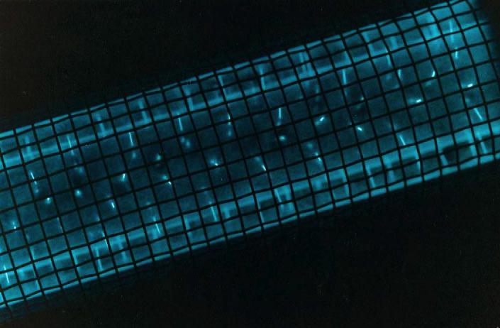
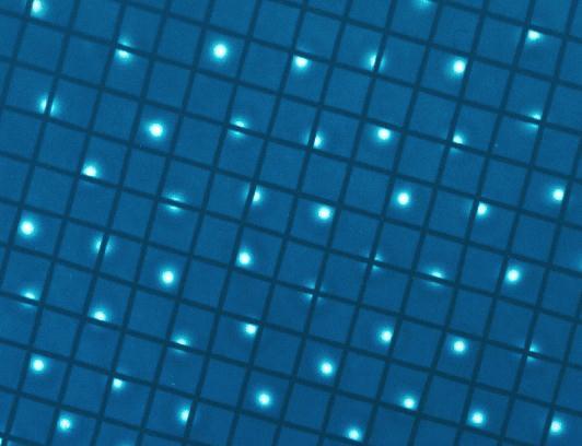
15 Cylindrical Excimer UV Source
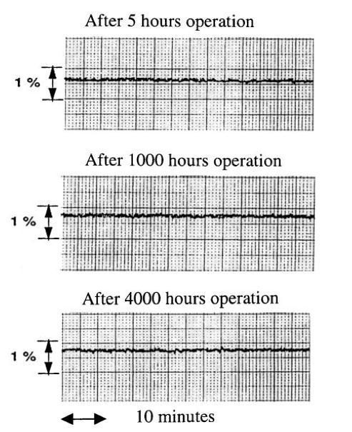

16 Efficiency & Long term stability: 222nm
17 Excimer lamp: Characteristic features o Incoherent, almost monochromatic, more than 20 wavelengths, high UV and VUV intensities o Robust and inexpensive, ecologically beneficial (Hg free) o Long stable lifetime o No self-absorption, high efficiency o o Easy to handle, no major cooling Scalable - large areas possible (cm 2 -m 2 )..
18 Bond Dissociation Energy of Covalent Bonds and Wavelengths of Excimer UV Radiation
19 Bond Dissociation Energy of Covalent Bonds and Wavelengths of Excimer UV Radiation.lots of available photochemistry!
20 Outline of Talk 1. Principles & properties of UV Excimer Lamps 2. Development of UV deposition system 3. Potential Applications: Surface engineering Oxide, metal deposition Interface engineering Nanoparticle deposition & doping


21 Lamp Chamber Reactor Chamber


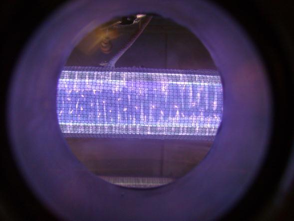
22 Large area excimer lamp system
23 Uniformity modelling of three lamp system
24 UV intensity (W/m ) 2 UV intensity profile of three lamp system cm from lamps Extent of 100 mm wafer edge of left lamp center of middle lamp Distance (cm) edge of right lamp
25 Outline of Talk 1. Principles & properties of UV Excimer Lamps 2. Development of UV deposition system 3. Potential Applications: Surface engineering Oxide, metal deposition Interface engineering Nanoparticle deposition & doping
26 Outline of Talk 1. Principles & properties of UV Excimer Lamps 2. Development of UV deposition system 3. Potential Applications: Surface engineering Oxide, metal deposition Interface engineering Nanoparticle deposition & doping
27 Treatment of Polymer Surfaces Low UV irradiation Polymer c leaning Polymerisation, cross-linking Oxidation, bond/chain breaking Fluence Surface modification, roughening Removal by laser ablation or photoetching High Hole drilling


28 VUV Surface Modification of Polymide: 126nm Non-irradiated 100nm 20 seconds No-irradiation 60 seconds 120 seconds, 126 nm lamp 120 seconds, 126 nm lamp XPS results show photo-dissociation of imide groups in Polyimide during 126 nm VUV irradiation
29 UV Surface modification of PET Surface changes of PET irradiated for different times with a 222nm excimer lamp

30 UV Surface modification of PET Surface changes of PET irradiated for different times with a 222nm excimer lamp.can be used to promote surface adhesion
31 Patterned Treatment of Polymer Surfaces


32 Copper structures on aluminium nitride 5 µm
33 Photo-oxidation of Silicon: Si +h + O2
34 Bond Dissociation Energy of Covalent Bonds and Wavelengths of Excimer UV Radiation O 2


35 Emission spectrum of the second excimer continua of Ar 2 * rare gas dimer Wavelength (nm)
36 FTIR spectra of SiO 2 grown by 126nm excimer lamp at room temperature
37 Thickness (nm) Growth of SiO 2 with 126 nm excimer radiation: 15 10
38 Thickness (nm) Growth of SiO 2 with 126 nm excimer radiation: Room Temperature! 15 10
39 126nm Oxidation: Summary Successful room temperature oxidation of Si using 126nm radiation XPS and FTIR confirm high quality and stoichiometric SiO 2 formed. Leakage current densities as low as 5 x10⁻⁸ A/cm 2 at an applied electric field of 1 MV/cm. Significant oxidation rates, as high as 8 nm/min achieved. Thicknesses up to 24 nm readily obtained with no growth saturation. Rapid oxidation related to creation of aggressive O 1S oxidant.
40 Photo-oxidation of Silicon-Germanium
41 High-resolution XTEM image of UV Oxidised SiGe
42 High-resolution XTEM image of UV Oxidised SiGe
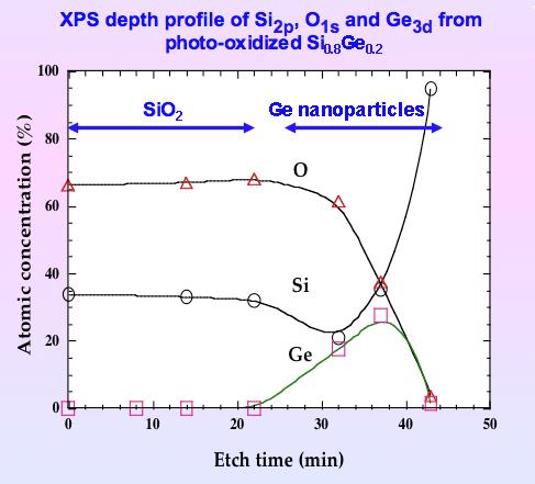
43 High-resolution XTEM image of UV Oxidised SiGe
44 Outline of Talk 1. Principles & properties of UV Excimer Lamps 2. Development of UV deposition system 3. Potential Applications: Surface engineering Oxide, metal deposition Interface engineering Nanoparticle deposition & doping
45 Photo DEPOSITION of Dielectrics
46 Photo-CVD Apparatus UV Lamp Chamber Precursors UV SiH 4, O 2, N 2 O, NH 3 Wafer Shower head Processing Chamber Sample heater To pumps
47 Deposition of Si oxide, oxynitride, and nitride using SiH 4 with various N 2 O/NH 3 precursor ratios Wavenumber (cm -1 )

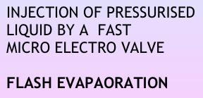
48 Metal Oxide Deposition: Photo-CVD reactor incorporating bubbler/digital liquid injection & designer precursors Designer Precursor
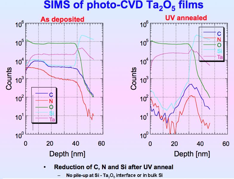
49 Excimer lamp deposition of metal oxides using UV-Injection Liquid Source (UVILS): TiO 2 Ta 2 O 5 HfO 2
50 Excimer lamp deposition of metal oxides using UV-Injection Liquid Source (UVILS): TiO 2 Ta 2 O 5 HfO 2
 Et : CH 3 - CH 2 Me: CH 3 EtO EtO EtO Ta EtO O N CH 2 CH 2 Me")
51 Tantalum Precursor Tetra ethoxy (dimethyl amino ethoxy) tantalum Ta (OEt) 4 (O CH 2 CH 2 N Me 2 ) Et : CH 3 - CH 2 Me: CH 3 EtO EtO EtO Ta EtO O N CH 2 CH 2 Me Me

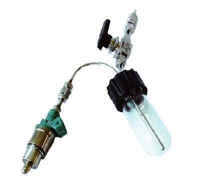
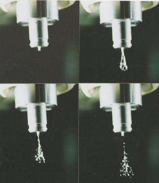
52 Precursor Injector
53 T ox (nm) UVILS-CVD: Ta 2 O Thickness (nm) 2.5 Å / injection Number of drops
54 Thickness (Å) Refractive index Uniformity of UV processed Ta 2 O 5 films Thickness: < 1.7% Refractive index: 2.09±0.004 (< 0.43%) Distance across a 4 inch wafer (cm)
55 lnr (nm/min) Growth rate of photo- and thermal- CVD of Ta 2 O 5 films C 400 C 300 C 200 C Photo-CVD Thermal-CVD 2 1 E a =1.97 ev E a =0.078 ev /T (1000/K)
56 Transmittance (a.u.) FTIR spectra for for Ta 2 O 5 films deposited by photo-cvd at 350 C and UV annealed at 400 C as-deposited suboxides 0.5h annealing 1.0h annealing Ta-O 10% Si-O Wavenumber (cm -1 )
57 The SiO 2 interface layer: UV Annealing As deposited 15 mins 25 mins 40 mins

58 The SiO 2 interface layer: UV Annealing As deposited 15 mins 25 mins 40 mins.can the interfacial oxide be reduced?
59 Outline of Talk 1. Principles & properties of UV Excimer Lamps 2. Development of UV deposition system 3. Potential Applications: Surface engineering Oxide, metal deposition Interface engineering Nanoparticle deposition & doping


60 Suppression of interface oxide by Predeposition UV-anneal in N 2 O 0 minutes 10 minutes 20 minutes Demonstrated previously, BUT typically T > 800 o C Pre photo-cvd at 350 o C
61
62 Comparison of leakage current densities in Ta 2 O 5 films obtained by different methods CVD 1) Plasma - CVD 2) Photo - CVD (our work) 3) Leakage current density at 1 MV/cm (A/cm 2 ) Deposited or annealed temp annealing annealing asdeposited asdeposited asdeposited annealing x x C 800 C 500 C 700 C 350 C 400 C
63 Summary Snapshot overview of UV excimer lamp technology Example applications towards low temperature deposition of high quality electronic films demonstrated Rapid photo-oxidation Photo-deposition of dielectrics Metallization & nanocrystalline formation Surface modification & patterning NC-embedded matrices Applications in many other areas Surface modification, crystallisation Packaging Pollution control & Water treatment Curing of Paints, Varnishes, Coatings, Dry lithography, Printing Biological/Medical..

64 Thank you for your attention!
Development of an excimer UV light source system for water treatment
 Development of an excimer UV light source system for water treatment Zoran Falkenstein Ushio America, Inc. May 2001 Zoran Falkenstein Development of an excimer UV light source system for water treatment
Excimer Lasers Currently best UV laser sources Consist two atom types which repel each other eg nobel gas and halide or oxide which normally do not
 Excimer Lasers Currently best UV laser sources Consist two atom types which repel each other eg nobel gas and halide or oxide which normally do not bond But when excited/ionized these atoms attract Bound
A KINETIC MODEL FOR EXCIMER UV AND VUV RADIATION IN DIELECTRIC BARRIER DISCHARGES*
 A KINETIC MODEL FOR EXCIMER UV AND VUV RADIATION IN DIELECTRIC BARRIER DISCHARGES* Xudong Peter Xu and Mark J. Kushner University of Illinois Department of Electrical and Computer Engineering Urbana, IL
Eximer Lasers UV laser sources Consist two atom types which repel each other eg nobel gas and halide or oxide When excited/ionized atoms attract
 Eximer Lasers UV laser sources Consist two atom types which repel each other eg nobel gas and halide or oxide When excited/ionized atoms attract Bound together separated by short distance Call this Excited
J. Price, 1,2 Y. Q. An, 1 M. C. Downer 1 1 The university of Texas at Austin, Department of Physics, Austin, TX
 Understanding process-dependent oxygen vacancies in thin HfO 2 /SiO 2 stacked-films on Si (100) via competing electron-hole injection dynamic contributions to second harmonic generation. J. Price, 1,2
CVD: General considerations.
 CVD: General considerations. PVD: Move material from bulk to thin film form. Limited primarily to metals or simple materials. Limited by thermal stability/vapor pressure considerations. Typically requires
Photocatalysis: semiconductor physics
 Photocatalysis: semiconductor physics Carlos J. Tavares Center of Physics, University of Minho, Portugal ctavares@fisica.uminho.pt www.fisica.uminho.pt 1 Guimarães Where do I come from? 3 Guimarães 4 Introduction>>
Fabrication Technology, Part I
 EEL5225: Principles of MEMS Transducers (Fall 2004) Fabrication Technology, Part I Agenda: Microfabrication Overview Basic semiconductor devices Materials Key processes Oxidation Thin-film Deposition Reading:
ARGON EXCIMER LAMP. A. Sobottka, L. Prager, L. Drößler, M. Lenk. Leibniz Institute of Surface Modification
 ARGON EXCIMER LAMP A. Sobottka, L. Prager, L. Drößler, M. Lenk 1 Introduction Ar-Zufuhr Excimer-Plasma Inertisierung Polymerfolie Sintermetall Inertisierung Post curing [1] EP 1050395 A2 2 Introduction
Excimer Lasers Currently best UV laser sources Consist two atom types which repel each other eg nobel gas and halide or oxide which normally do not
 Excimer Lasers Currently best UV laser sources Consist two atom types which repel each other eg nobel gas and halide or oxide which normally do not bond But when excited/ionized these atoms attract Bound
Intensity / a.u. 2 theta / deg. MAPbI 3. 1:1 MaPbI 3-x. Cl x 3:1. Supplementary figures
 Intensity / a.u. Supplementary figures 110 MAPbI 3 1:1 MaPbI 3-x Cl x 3:1 220 330 0 10 15 20 25 30 35 40 45 2 theta / deg Supplementary Fig. 1 X-ray Diffraction (XRD) patterns of MAPbI3 and MAPbI 3-x Cl
Physics of Organic Semiconductor Devices: Materials, Fundamentals, Technologies and Applications
 Physics of Organic Semiconductor Devices: Materials, Fundamentals, Technologies and Applications Dr. Alex Zakhidov Assistant Professor, Physics Department Core faculty at Materials Science, Engineering
Ar and Kr ion lasers
 Types of Lasers Ar and Kr ion lasers Nd:YAG and Nd:YLF lasers CO 2 lasers Excimer lasers Dye lasers Transition metal lasers Optical parametric amplification Ar and Kr ion lasers Noble gas ions are created
Modern Methods in Heterogeneous Catalysis Research: Preparation of Model Systems by Physical Methods
 Modern Methods in Heterogeneous Catalysis Research: Preparation of Model Systems by Physical Methods Methods for catalyst preparation Methods discussed in this lecture Physical vapour deposition - PLD
Ion Beam Induced Luminescence (IBIL) for scintillator analysis
 for scintillator analysis") Ion Beam Induced Luminescence (IBIL) for scintillator analysis Alberto Quaranta Università di Trento Dipartimento dei Materiali e delle Tecnologie Industriali (DIMTI) Laboratori Nazionali di Legnaro -
Ion Beam Induced Luminescence (IBIL) for scintillator analysis Alberto Quaranta Università di Trento Dipartimento dei Materiali e delle Tecnologie Industriali (DIMTI) Laboratori Nazionali di Legnaro -
A Plasmonic Photocatalyst Consisting of Silver Nanoparticles Embedded in Titanium Dioxide. Ryan Huschka LANP Seminar February 19, 2008
 A Plasmonic Photocatalyst Consisting of Silver Nanoparticles Embedded in Titanium Dioxide Ryan Huschka LANP Seminar February 19, 2008 TiO 2 Applications White Pigment Photocatalyst Previous methods to
Introducing the RoVaCBE Flagship project: Roll-to-roll Vacuum-processed Carbon Based Electronics. Dr Hazel Assender, University of Oxford
 Introducing the RoVaCBE Flagship project: Roll-to-roll Vacuum-processed Carbon Based Electronics Dr Hazel Assender, University of Oxford DALMATIAN TECHNOLOGY 21 st Sept 2010 1 Organic electronics Opportunity
Photovoltaic cell and module physics and technology
 Photovoltaic cell and module physics and technology Vitezslav Benda, Prof Czech Technical University in Prague benda@fel.cvut.cz www.fel.cvut.cz 6/21/2012 1 Outlines Photovoltaic Effect Photovoltaic cell
Supplementary Figure 1 XRD pattern of a defective TiO 2 thin film deposited on an FTO/glass substrate, along with an XRD pattern of bare FTO/glass
 Supplementary Figure 1 XRD pattern of a defective TiO 2 thin film deposited on an FTO/glass substrate, along with an XRD pattern of bare FTO/glass and a reference pattern of anatase TiO 2 (JSPDS No.: 21-1272).
EE C245 ME C218 Introduction to MEMS Design Fall 2007
 EE C245 ME C218 Introduction to MEMS Design Fall 2007 Prof. Clark T.-C. Nguyen Dept. of Electrical Engineering & Computer Sciences University of California at Berkeley Berkeley, CA 94720 Lecture 4: Film
Lasers E 6 E 4 E 3 E 2 E 1
 Lasers Laser is an acronym for light amplification by stimulated emission of radiation. Here the process of stimulated emission is used to amplify light radiation. Spontaneous emission: When energy is
Photolithography II ( Part 1 )
") 1 Photolithography II ( Part 1 ) Chapter 14 : Semiconductor Manufacturing Technology by M. Quirk & J. Serda Bjørn-Ove Fimland, Department of Electronics and Telecommunication, Norwegian University of Science
1 Photolithography II ( Part 1 ) Chapter 14 : Semiconductor Manufacturing Technology by M. Quirk & J. Serda Bjørn-Ove Fimland, Department of Electronics and Telecommunication, Norwegian University of Science
Chapter 6. Summary and Conclusions
 Chapter 6 Summary and Conclusions Plasma deposited amorphous hydrogenated carbon films (a-c:h) still attract a lot of interest due to their extraordinary properties. Depending on the deposition conditions
Chapter 2 On-wafer UV Sensor and Prediction of UV Irradiation Damage
 Chapter 2 On-wafer UV Sensor and Prediction of UV Irradiation Damage Abstract UV radiation during plasma processing affects the surface of materials. Nevertheless, the interaction of UV photons with surface
Plasma Deposition (Overview) Lecture 1
 Lecture 1") Plasma Deposition (Overview) Lecture 1 Material Processes Plasma Processing Plasma-assisted Deposition Implantation Surface Modification Development of Plasma-based processing Microelectronics needs (fabrication
Plasma Deposition (Overview) Lecture 1 Material Processes Plasma Processing Plasma-assisted Deposition Implantation Surface Modification Development of Plasma-based processing Microelectronics needs (fabrication
DEPOSITION OF THIN TiO 2 FILMS BY DC MAGNETRON SPUTTERING METHOD
 Chapter 4 DEPOSITION OF THIN TiO 2 FILMS BY DC MAGNETRON SPUTTERING METHOD 4.1 INTRODUCTION Sputter deposition process is another old technique being used in modern semiconductor industries. Sputtering
DUV ( nm ) Characterization of Materials: A new instrument, the Purged UV Spectroscopic Ellipsometer,
 Characterization of Materials: A new instrument, the Purged UV Spectroscopic Ellipsometer,") WISE 2000, International Workshop on Spectroscopic Ellipsometry, 8 9 May 2000 DUV (150 350nm ) Characterization of Materials: A new instrument, the Purged UV Spectroscopic Ellipsometer, Pierre BOHER,,
WISE 2000, International Workshop on Spectroscopic Ellipsometry, 8 9 May 2000 DUV (150 350nm ) Characterization of Materials: A new instrument, the Purged UV Spectroscopic Ellipsometer, Pierre BOHER,,
Top down and bottom up fabrication
 Lecture 24 Top down and bottom up fabrication Lithography ( lithos stone / graphein to write) City of words lithograph h (Vito Acconci, 1999) 1930 s lithography press Photolithography d 2( NA) NA=numerical
Plasma based modification of thin films and nanoparticles. Johannes Berndt, GREMI,Orléans
 Plasma based modification of thin films and nanoparticles Johannes Berndt, GREMI,Orléans What is a plasma? A plasma is a ionized quasineutral gas! + electron electrons Neon bottle Ne atom Ne ion: Ne +
Lecture 6. Rapid Thermal Processing. Reading: Chapter 6
 Lecture 6 Rapid Thermal Processing Reading: Chapter 6 (Chapter 6) Categories: Rapid Thermal Anneal (RTA) Rapid Thermal Oxidation (RTO) Rapid Thermal Nitridation (RTN) (and oxynitrides) Rapid Thermal Diffusion
Case Study of Electronic Materials Packaging with Poor Metal Adhesion and the Process for Performing Root Cause Failure Analysis
 Case Study of Electronic Materials Packaging with Poor Metal Adhesion and the Process for Performing Root Cause Failure Analysis Dr. E. A. Leone BACKGRUND ne trend in the electronic packaging industry
Far IR (FIR) Gas Lasers microns wavelengths, THz frequency Called Terahertz lasers or FIR lasers At this wavelength behaves more like
 Gas Lasers microns wavelengths, THz frequency Called Terahertz lasers or FIR lasers At this wavelength behaves more like") Far IR (FIR) Gas Lasers 10-1500 microns wavelengths, 300 10 THz frequency Called Terahertz lasers or FIR lasers At this wavelength behaves more like microwave signal than light Created by Molecular vibronic
Far IR (FIR) Gas Lasers 10-1500 microns wavelengths, 300 10 THz frequency Called Terahertz lasers or FIR lasers At this wavelength behaves more like microwave signal than light Created by Molecular vibronic
Chapter 7. Plasma Basics
 Chapter 7 Plasma Basics 2006/4/12 1 Objectives List at least three IC processes using plasma Name three important collisions in plasma Describe mean free path Explain how plasma enhance etch and CVD processes
Ultrafast X-Ray-Matter Interaction and Damage of Inorganic Solids October 10, 2008
 Ultrafast X-Ray-Matter Interaction and Damage of Inorganic Solids October 10, 2008 Richard London rlondon@llnl.gov Workshop on Interaction of Free Electron Laser Radiation with Matter Hamburg This work
Far IR Gas Lasers microns wavelengths, THz frequency Called Terahertz lasers or FIR lasers At this wavelength behaves more like
 Far IR Gas Lasers 10-1500 microns wavelengths, 300 10 THz frequency Called Terahertz lasers or FIR lasers At this wavelength behaves more like microwave signal than light Created by Molecular vibronic
Luminescence basics. Slide # 1
 Luminescence basics Types of luminescence Cathodoluminescence: Luminescence due to recombination of EHPs created by energetic electrons. Example: CL mapping system Photoluminescence: Luminescence due to
CHAPTER 6: Etching. Chapter 6 1
 Chapter 6 1 CHAPTER 6: Etching Different etching processes are selected depending upon the particular material to be removed. As shown in Figure 6.1, wet chemical processes result in isotropic etching
CVD-3 MFSIN-HU-2 SiN x Mixed Frequency Process
 CVD-3 MFSIN-HU-2 SiN x Mixed Frequency Process Standard MFSIN-HU-2 Process Top C Bottom C Pump to Base Time (s) SiH 4 Flow HF/ LF NH 3 Flow HF/LF N 2 HF/LF HF (watts) LF (watts) HF Time LF Time Pressure
X-Ray Photoelectron Spectroscopy (XPS) Prof. Paul K. Chu
 Prof. Paul K. Chu") X-Ray Photoelectron Spectroscopy (XPS) Prof. Paul K. Chu X-ray Photoelectron Spectroscopy Introduction Qualitative analysis Quantitative analysis Charging compensation Small area analysis and XPS imaging
X-Ray Photoelectron Spectroscopy (XPS) Prof. Paul K. Chu X-ray Photoelectron Spectroscopy Introduction Qualitative analysis Quantitative analysis Charging compensation Small area analysis and XPS imaging
Stretching the Barriers An analysis of MOSFET Scaling. Presenters (in order) Zeinab Mousavi Stephanie Teich-McGoldrick Aseem Jain Jaspreet Wadhwa
 Zeinab Mousavi Stephanie Teich-McGoldrick Aseem Jain Jaspreet Wadhwa") Stretching the Barriers An analysis of MOSFET Scaling Presenters (in order) Zeinab Mousavi Stephanie Teich-McGoldrick Aseem Jain Jaspreet Wadhwa Why Small? Higher Current Lower Gate Capacitance Higher
Stretching the Barriers An analysis of MOSFET Scaling Presenters (in order) Zeinab Mousavi Stephanie Teich-McGoldrick Aseem Jain Jaspreet Wadhwa Why Small? Higher Current Lower Gate Capacitance Higher
Phys 2310 Fri. Dec. 12, 2014 Today s Topics. Begin Chapter 13: Lasers Reading for Next Time
 Phys 2310 Fri. Dec. 12, 2014 Today s Topics Begin Chapter 13: Lasers Reading for Next Time 1 Reading this Week By Fri.: Ch. 13 (13.1, 13.3) Lasers, Holography 2 Homework this Week No Homework this chapter.
Chemistry Instrumental Analysis Lecture 3. Chem 4631
 Chemistry 4631 Instrumental Analysis Lecture 3 Quantum Transitions The energy of a photon can also be transferred to an elementary particle by adsorption if the energy of the photon exactly matches the
Pulsed lasers. To induce new chemistry, different from that initiated by conventional sources
 Pulsed lasers As part of a method to study photoinitiated chemical reactions To induce new chemistry, different from that initiated by conventional sources As a light source, to initiate the same chemistry
Chemistry Instrumental Analysis Lecture 17. Chem 4631
 Chemistry 4631 Instrumental Analysis Lecture 17 Introduction to Optical Atomic Spectrometry From molecular to elemental analysis there are three major techniques used for elemental analysis: Optical spectrometry
Abstract... I. Acknowledgements... III. Table of Content... V. List of Tables... VIII. List of Figures... IX
 Abstract... I Acknowledgements... III Table of Content... V List of Tables... VIII List of Figures... IX Chapter One IR-VUV Photoionization Spectroscopy 1.1 Introduction... 1 1.2 Vacuum-Ultraviolet-Ionization
Chapter 7 Plasma Basic
 Chapter 7 Plasma Basic Hong Xiao, Ph. D. hxiao89@hotmail.com www2.austin.cc.tx.us/hongxiao/book.htm Hong Xiao, Ph. D. www2.austin.cc.tx.us/hongxiao/book.htm 1 Objectives List at least three IC processes
X-Rays From Laser Plasmas
 X-Rays From Laser Plasmas Generation and Applications I. C. E. TURCU CLRC Rutherford Appleton Laboratory, UK and J. B. DANCE JOHN WILEY & SONS Chichester New York Weinheim Brisbane Singapore Toronto Contents
CVD-3 MFSIN-HU-1 SiN x Mixed Frequency Process
 CVD-3 MFSIN-HU-1 SiN x Mixed Frequency Process Standard MFSIN-HU-1 Process Top C Bottom C Pump to Base Time (s) SiH 4 Flow HF/ LF NH 3 Flow HF/LF N 2 HF/LF HF (watts) LF (watts) HF Time LF Time Pressure
3.155J/6.152J Microelectronic Processing Technology Fall Term, 2004
 3.155J/6.152J Microelectronic Processing Technology Fall Term, 2004 Bob O'Handley Martin Schmidt Quiz Nov. 17, 2004 Ion implantation, diffusion [15] 1. a) Two identical p-type Si wafers (N a = 10 17 cm
Self-study problems and questions Processing and Device Technology, FFF110/FYSD13
 Self-study problems and questions Processing and Device Technology, FFF110/FYSD13 Version 2016_01 In addition to the problems discussed at the seminars and at the lectures, you can use this set of problems
Auger Electron Spectroscopy (AES)
") 1. Introduction Auger Electron Spectroscopy (AES) Silvia Natividad, Gabriel Gonzalez and Arena Holguin Auger Electron Spectroscopy (Auger spectroscopy or AES) was developed in the late 1960's, deriving
1. Introduction Auger Electron Spectroscopy (AES) Silvia Natividad, Gabriel Gonzalez and Arena Holguin Auger Electron Spectroscopy (Auger spectroscopy or AES) was developed in the late 1960's, deriving
EE-612: Lecture 22: CMOS Process Steps
 EE-612: Lecture 22: CMOS Process Steps Mark Lundstrom Electrical and Computer Engineering Purdue University West Lafayette, IN USA Fall 2006 NCN www.nanohub.org Lundstrom EE-612 F06 1 outline 1) Unit Process
Because light behaves like a wave, we can describe it in one of two ways by its wavelength or by its frequency.
 Light We can use different terms to describe light: Color Wavelength Frequency Light is composed of electromagnetic waves that travel through some medium. The properties of the medium determine how light
Supplementary Figure S1. Verifying the CH 3 NH 3 PbI 3-x Cl x sensitized TiO 2 coating UV-vis spectrum of the solution obtained by dissolving the
 Supplementary Figure S1. Verifying the CH 3 NH 3 PbI 3-x Cl x sensitized TiO 2 coating UV-vis spectrum of the solution obtained by dissolving the spiro-ometad from a perovskite-filled mesoporous TiO 2
Starting solution. Hydrolysis reaction under thermostatic conditions. Check of viscosity and deposition test SOL. Deposition by spin coating
 Supplementary Figures Tetramethyl orthosilicate (TMOS) Tetrahydrofuran anhydrous (THF) Trimethyl methoxy silane (TMMS) Trimethyl silil acetate (TMSA) Starting solution Hydrolysis reaction under thermostatic
Tailored surface modification of substrates by atmospheric plasma for improved compatibility with specific adhesive Nicolas Vandencasteele
 1 oating Plasma Innovation Tailored surface modification of substrates by atmospheric plasma for improved compatibility with specific adhesive Nicolas Vandencasteele 2 Plasma Applications Adhesion improvement
Lecture 6 Plasmas. Chapters 10 &16 Wolf and Tauber. ECE611 / CHE611 Electronic Materials Processing Fall John Labram 1/68
 Lecture 6 Plasmas Chapters 10 &16 Wolf and Tauber 1/68 Announcements Homework: Homework will be returned to you on Thursday (12 th October). Solutions will be also posted online on Thursday (12 th October)
as-deposited and low temperature annealed Si-rich SiO 2 films
 Excitation wavelength-independent sensitized Er 3+ concentration in as-deposited and low temperature annealed Si-rich SiO 2 films Oleksandr Savchyn, 1,a) Ravi M. Todi, 2 Kevin R. Coffey, 2,3 Luis K. Ono
"What Do I Remember From Introductory Chemistry?" - A Problem Set
 1 "What Do I Remember From Introductory Chemistry?" - A Problem Set These problems review a portion of the material from introductory chemistry that you should be very familiar with. 1. The electron configuration
CVD-3 LFSIN SiN x Process
 CVD-3 LFSIN SiN x Process Top Electrode, C Bottom Electrode, C Pump to Base Time (s) SiH 4 Flow Standard LFSIN Process NH 3 Flow N 2 HF (watts) LF (watts) Pressure (mtorr Deposition Time min:s.s Pump to
Low temperature anodically grown silicon dioxide films for solar cell. Nicholas E. Grant
 Low temperature anodically grown silicon dioxide films for solar cell applications Nicholas E. Grant Outline 1. Electrochemical cell design and properties. 2. Direct-current current anodic oxidations-part
Core Level Spectroscopies
 Core Level Spectroscopies Spectroscopies involving core levels are element-sensitive, and that makes them very useful for understanding chemical bonding, as well as for the study of complex materials.
Diagnósticos em Plasmas
 Tecnologia a Plasma para o Processamento de Materiais Diagnósticos em Plasmas Diagnósticos Ópticos João Santos Sousa, nº50901 Semestre Inverno 2004/2005 21 de Janeiro de 2005, 9h-10h, sala F8 Contents
Clean-Room microfabrication techniques. Francesco Rizzi Italian Institute of Technology
 Clean-Room microfabrication techniques Francesco Rizzi Italian Institute of Technology Miniaturization The first transistor Miniaturization The first transistor Miniaturization The first transistor Miniaturization
Catalytic materials for plasma-based VOC removal
 Catalytic materials for plasma-based VOC removal David Cameron, Tatyana Ivanova, Marja-Leena Kääriäinen Advanced Surface Technology Research Laboratory (ASTRaL) Lappeenranta University of Technology Finland
Atmospheric pressure Plasma Enhanced CVD for large area deposition of TiO 2-x electron transport layers for PV. Heather M. Yates
 Atmospheric pressure Plasma Enhanced CVD for large area deposition of TiO 2-x electron transport layers for PV Heather M. Yates Why the interest? Perovskite solar cells have shown considerable promise
Chapter 3 Engineering Science for Microsystems Design and Fabrication
 Lectures on MEMS and MICROSYSTEMS DESIGN and MANUFACTURE Chapter 3 Engineering Science for Microsystems Design and Fabrication In this Chapter, we will present overviews of the principles of physical and
Surface modification of polyethylene terephthalate (PET) and oxide coated PET for adhesion improvement
 and oxide coated PET for adhesion improvement") Surface modification of polyethylene terephthalate (PET) and oxide coated PET for adhesion improvement AIMCAL 2016 Dresden Juliane Fichtner Tobias Beck Frank Simon (IPF, Dresden) page 1 Motivation oxygen
Surface modification of polyethylene terephthalate (PET) and oxide coated PET for adhesion improvement AIMCAL 2016 Dresden Juliane Fichtner Tobias Beck Frank Simon (IPF, Dresden) page 1 Motivation oxygen
10/2/2008. hc λ. νλ =c. proportional to frequency. Energy is inversely proportional to wavelength And is directly proportional to wavenumber
 CH217 Fundamentals of Analytical Chemistry Module Leader: Dr. Alison Willows Electromagnetic spectrum Properties of electromagnetic radiation Many properties of electromagnetic radiation can be described
The design of an integrated XPS/Raman spectroscopy instrument for co-incident analysis
 The design of an integrated XPS/Raman spectroscopy instrument for co-incident analysis Tim Nunney The world leader in serving science 2 XPS Surface Analysis XPS +... UV Photoelectron Spectroscopy UPS He(I)
Two-dimensional lattice
 Two-dimensional lattice a 1 *, k x k x =0,k y =0 X M a 2, y Γ X a 2 *, k y a 1, x Reciprocal lattice Γ k x = 0.5 a 1 *, k y =0 k x = 0, k y = 0.5 a 2 * k x =0.5a 1 *, k y =0.5a 2 * X X M k x = 0.25 a 1
CHEM1901/ J-5 June 2013
 CHEM1901/3 2013-J-5 June 2013 Oxygen exists in the troposphere as a diatomic molecule. 4 (a) Using arrows to indicate relative electron spin, fill the left-most valence orbital energy diagram for O 2,
Phys 2310 Mon. Dec. 4, 2017 Today s Topics. Begin supplementary material: Lasers Reading for Next Time
 Phys 2310 Mon. Dec. 4, 2017 Today s Topics Begin supplementary material: Lasers Reading for Next Time 1 By Wed.: Reading this Week Lasers, Holography 2 Homework this Week No Homework this chapter. Finish
UNIVERSITY OF CALIFORNIA College of Engineering Department of Electrical Engineering and Computer Sciences. Fall Exam 1
 UNIVERSITY OF CALIFORNIA College of Engineering Department of Electrical Engineering and Computer Sciences EECS 143 Fall 2008 Exam 1 Professor Ali Javey Answer Key Name: SID: 1337 Closed book. One sheet
Laser Dissociation of Protonated PAHs
 100 Chapter 5 Laser Dissociation of Protonated PAHs 5.1 Experiments The photodissociation experiments were performed with protonated PAHs using different laser sources. The calculations from Chapter 3
Chapter 15 Molecular Luminescence Spectrometry
 Chapter 15 Molecular Luminescence Spectrometry Two types of Luminescence methods are: 1) Photoluminescence, Light is directed onto a sample, where it is absorbed and imparts excess energy into the material
Introduction. Photoresist : Type: Structure:
 Photoresist SEM images of the morphologies of meso structures and nanopatterns on (a) a positively nanopatterned silicon mold, and (b) a negatively nanopatterned silicon mold. Introduction Photoresist
Characterization of Charge Trapping and Dielectric Breakdown of HfAlOx/SiON Dielectric Gate Stack
 Characterization of Charge Trapping and Dielectric Breakdown of HfAlOx/SiON Dielectric Gate Stack Y. Pei, S. Nagamachi, H. Murakami, S. Higashi, S. Miyazaki, T. Kawahara and K. Torii Graduate School of
Nanostructures Fabrication Methods
 Nanostructures Fabrication Methods bottom-up methods ( atom by atom ) In the bottom-up approach, atoms, molecules and even nanoparticles themselves can be used as the building blocks for the creation of
Materialwissenschaft und Nanotechnologie. Introduction to Lasers
 Materialwissenschaft und Nanotechnologie Introduction to Lasers Dr. Andrés Lasagni Lehrstuhl für Funktionswerkstoffe Sommersemester 007 1-Introduction to LASER Contents: Light sources LASER definition
Surface Hydrophilic Treatment of Polyester Films via UV irradiation
 Surface Hydrophilic Treatment of Polyester Films via UV irradiation Gwang Hoe Koo, Hae Sung Lee and Jinho Jang School of Advanced Materials and System Engineering, Kumoh National Institute of Technology,
MICROCHIP MANUFACTURING by S. Wolf
 by S. Wolf Chapter 15 ALUMINUM THIN-FILMS and SPUTTER-DEPOSITION 2004 by LATTICE PRESS CHAPTER 15 - CONTENTS Aluminum Thin-Films Sputter-Deposition Process Steps Physics of Sputter-Deposition Magnetron-Sputtering
Agenda. 1. Atomic Layer Deposition Technology
 Agenda 1. Atomic Layer Deposition Technology 2. What is ALD? Atomic Layer Deposition is invented in 1977 by T. Suntola et al. - New Deposition Method for Electro-Luminescent Display (ZnS:Mn Thin Films)
Steady state operation : g = 1
 Laser = active medium + cavity L active medium R1 R2 47 47 Net gain per round trip L active medium R1 R2 losses gain (intrinsic) g Intensity after one round trip = = R1$ R2$ exp6 2^b-ah $ l@ I0 Steady
GaN for use in harsh radiation environments
 4 th RD50 - Workshop on radiation hard semiconductor devices for very high luminosity colliders GaN for use in harsh radiation environments a (W Cunningham a, J Grant a, M Rahman a, E Gaubas b, J Vaitkus
Surface cleaning mechanisms utilizing VUV radiation in oxygen containing gaseous environments
 Surface cleaning mechanisms utilizing VUV radiation in oxygen containing gaseous environments Zoran Falkenstein Ushio America, Inc. Zoran Falkenstein Surface cleaning mechanisms utilizing VUV radiation
Electronic structure of transition metal high-k dielectrics: interfacial band offset energies for microelectronic devices
 Applied Surface Science 212 213 (2003) 563 569 Electronic structure of transition metal high-k dielectrics: interfacial band offset energies for microelectronic devices Gerald Lucovsky *, Gilbert B. Rayner
Introduction to Spectroscopic methods
 Introduction to Spectroscopic methods Spectroscopy: Study of interaction between light* and matter. Spectrometry: Implies a quantitative measurement of intensity. * More generally speaking electromagnetic
Etching: Basic Terminology
 Lecture 7 Etching Etching: Basic Terminology Introduction : Etching of thin films and sometimes the silicon substrate are very common process steps. Usually selectivity, and directionality are the first
Discover the Difference
 M-2000 Discover the Difference Focused M-2000 The M-2000 line of spectroscopic ellipsometers is engineered to meet the diverse demands of thin film characterization. An advanced optical design, wide spectral
4FNJDPOEVDUPS 'BCSJDBUJPO &UDI
 2010.5.4 1 Major Fabrication Steps in CMOS Process Flow UV light oxygen Silicon dioxide Silicon substrate Oxidation (Field oxide) photoresist Photoresist Coating Mask exposed photoresist Mask-Wafer Exposed
Lecture 0. NC State University
 Chemistry 736 Lecture 0 Overview NC State University Overview of Spectroscopy Electronic states and energies Transitions between states Absorption and emission Electronic spectroscopy Instrumentation Concepts
The Excimer Laser and Applications to Corneal Ablative Surgery
 The Excimer Laser and Applications to Corneal Ablative Surgery Peter M. Albrecht November 28, 2001 ECE 355 Final Project University of Illinois at Urbana-Champaign Introduction Excimer Excited Dimer A
Metal Vapour Lasers Use vapoured metal as a gain medium Developed by W. Silfvast (1966) Two types: Ionized Metal vapour (He-Cd) Neutral Metal vapour
 Two types: Ionized Metal vapour (He-Cd) Neutral Metal vapour") Metal Vapour Lasers Use vapoured metal as a gain medium Developed by W. Silfvast (1966) Two types: Ionized Metal vapour (He-Cd) Neutral Metal vapour (Cu) All operate by vaporizing metal in container Helium
Metal Vapour Lasers Use vapoured metal as a gain medium Developed by W. Silfvast (1966) Two types: Ionized Metal vapour (He-Cd) Neutral Metal vapour (Cu) All operate by vaporizing metal in container Helium
Supporting Information
 Supporting Information Dynamic Interaction between Methylammonium Lead Iodide and TiO 2 Nanocrystals Leads to Enhanced Photocatalytic H 2 Evolution from HI Splitting Xiaomei Wang,, Hong Wang,, Hefeng Zhang,,
Atmospheric Plasma treatment, effect on the plasma chemistry on adhesion Nicolas Vandencasteele
 1 oating Plasma Innovation Atmospheric Plasma treatment, effect on the plasma chemistry on adhesion Nicolas Vandencasteele 2 Plasma Applications Adhesion improvement onclusion 3 Plasma 4 th state of matter:
LECTURE 5 SUMMARY OF KEY IDEAS
 LECTURE 5 SUMMARY OF KEY IDEAS Etching is a processing step following lithography: it transfers a circuit image from the photoresist to materials form which devices are made or to hard masking or sacrificial
UNIAQ Department of Physics
 Nano4water, 2 nd dissemination Workshop Chalkidiki, 24-25 April 2012 Dr. Luca Lozzi Department of Physics University of L Aquila Italy UNIAQ Department of Physics N-doped TiO 2 nanostructured coatings
Etching Issues - Anisotropy. Dry Etching. Dry Etching Overview. Etching Issues - Selectivity
 Etching Issues - Anisotropy Dry Etching Dr. Bruce K. Gale Fundamentals of Micromachining BIOEN 6421 EL EN 5221 and 6221 ME EN 5960 and 6960 Isotropic etchants etch at the same rate in every direction mask
High speed vacuum deposition of organic TFTs in a roll-to-roll facility
 High speed vacuum deposition of organic TFTs in a roll-to-roll facility Dr Hazel Assender University of Oxford 1 Prof Martin Taylor Eifion Patchett, Aled Williams Prof Long Lin Prof Steve Yeates Dr John