Introduction to Nanotechnology-2
|
|
|
- William Nelson
- 6 years ago
- Views:
Transcription
1 Introduction to Nanotechnology-2 1 Prof.P. Ravindran, Department of Physics, Central University of Tamil Nadu, India & Center for Materials Science and Nanotechnology, University of Oslo, Norway
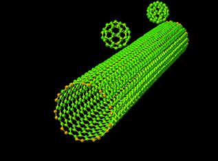
2 Nanoscale 2 No. Item Size (Approx.), Scaling down µm to nm Size (Approx.), on nm Scale 1. Human hair (diameter) µm 60, , Pollen µm 10, , Asbestos fibers (diameter) < 3 µm < 3, Diesel exhaust particles < 100 nm 1 µm < 100 nm Soot < 10 nm 1 µm < 10 nm Quantum dots 2 20 nm Nanotubes (diameter) ~1 nm ~ 1 8. Fullerenes ~ 1 nm ~ 1 9. Atoms 1-3 Å ~ 0.1 nm 1-3 Å ~ 0.1


3 Why nano will change the properties of materials? Example: Smaller size means larger surface area diameter 10 µm 50 nm diameter Area 0.22 m 2 /g 44 m 2 /g 3 3
4 Why nano will change the properties of materials? S/ V Smaller size means larger surface area R Sphere Volume, V = 4/3 π R 3 Surface Area, S = 4πR 2 Ratio S/V = 3 /R α 1/R He atom, 2R = 0.1 nm. S/V = R S/V R

 and etching away")
5 How to Make Nanostructures? 5 Top-down Approach Building something by starting with a larger component and carving away material (like a sculpture) In nanotechnology: patterning (using photolithography) and etching away material, as in building integrated circuits Rock Statue

6 Top-down approaches 6 These seek to create smaller devices by using larger ones to direct their assembly. Many technologies that descended from conventional solid-state silicon methods for fabricating microprocessors are now capable of creating features smaller than 100 nm, falling under the definition of nanotechnology. Giant magnetoresistance-based hard drives already on the market fit this description, as do atomic layer deposition (ALD) techniques.

7 Top-down approaches 7 Atomic force microscope tips can be used as a nanoscale "write head" to deposit a chemical upon a surface in a desired pattern in a process called dip pen nanolithography. This fits into the larger subfield of nanolithography. Solid-state techniques can also be used to create devices known as nanoelectromechanical systems or NEMS, which are related to microelectromechanical systems or MEMS.


8 Top-down approaches 8 Focused ion beams can directly remove material, or even deposit material when suitable pre-cursor gasses are applied at the same time. For example, this technique is used routinely to create sub-100 nm sections of material for analysis in Transmission electron microscopy.
, atom by atom assembly.")
9 How to Make Nanostructures? 9 Bottom-up Building something by assembling smaller components (like building a car engine), atom by atom assembly. In nanotechnology: self-assembly of atoms and molecules, as in chemical and biological systems Brick Building

10 Bottom-up approaches 10 These seek to arrange smaller components into more complex assemblies. DNA nanotechnology utilizes the specificity of Watson Crick basepairing to construct well-defined structures out of DNA and other nucleic acids. Approaches from the field of "classical" chemical synthesis also aim at designing molecules with well-defined shape (e.g. bis-peptides).

11 Bottom-up approaches 11 More generally, molecular self-assembly seeks to use concepts of supramolecular chemistry, and molecular recognition in particular, to cause single-molecule components to automatically arrange themselves into some useful conformation.

12 Functional approaches 12 These seek to develop components of a desired functionality without regard to how they might be assembled. Synthetic chemical methods can also be used to create what forensics call synthetic molecular motors, such as in a so-called nanocar.

13 Functional approaches 13 Molecular electronics seeks to develop molecules with useful electronic properties. These could then be used as single-molecule components in a nanoelectronic device. For an example see rotaxane. The Nokia Morph is a concept mobile phone created by Finnish company Nokia. The phone's theoretical feature list would include the ability to bend into numerous shapes, transparent electronics, self-cleaning surfaces and a wide range of fully integrated sensors.

14 14

15 Molecular self-assembly 15 Molecular self-assembly is the process by which molecules adopt a defined arrangement without guidance or management from an outside source. There are two types of self-assembly: Intramolecular self-assembly folding Intermolecular self-assembly. An example of a molecular self-assembly through hydrogen bonds reported by Meijer and coworkers. 15

16 16
17 17 Supramolecular Systems Molecular self-assembly is a key concept in supramolecular chemistry since assembly of the molecules is directed through noncovalent interactions (e.g., hydrogen bonding, metal coordination, hydrophobic forces, van der Waals forces, π-π interactions, and/or electrostatic) as well as electromagnetic interactions. Common examples include the formation of micelles, vesicles and liquid crystal phases. 17


18 Biology as a template 18 Biological systems are most effective and efficient manufacturing systems known: DNA polymerase: reliable replication, with error rate ~ 1 in 10,000,000,000 F1F0 ATP synthase: most efficient motor known (~90-100%)


19 Biology as a template 19 Based on simple processes (e.g. polymerisation) Create one basic geometry (linear chains) Rely on self-interactions to generate functional structures automatically ( self-assembly, folding in biology) But we still can t reliably predict folding for known structures after decades of intensive research! How do we design, de novo, both novel chemistries or functions, and the folds protein folds to achieve them?
20 20 Biological Systems Molecular self-assembly is crucial to the function of cells. It is exhibited in the self-assembly of lipids to form the membrane, the formation of double helical DNA through hydrogen bonding of the individual strands, and the assembly of proteins to form quaternary structures. Molecular self-assembly of incorrectly folded proteins into insoluble amyloid fibers is responsible for infectious prion-related neurodegenerative diseases. 20

21 21 Nanotechnology The DNA structure at left will self-assemble into the structure visualized by atomic force microscopy at right. 21
22 22 Nanotechnology Molecular Self assembly Molecular self-assembly is an important aspect of bottom-up approaches to nanotechnology. Using molecular self-assembly the final (desired) structure is programmed in the shape and functional groups of the molecules. Self-assembly is referred to as a 'bottom-up' manufacturing technique in contrast to a 'top-down' technique such as lithography where the desired final structure is carved from a larger block of matter. In the speculative vision of molecular nanotechnology, microchips of the future might be made by molecular self-assembly. An advantage to constructing nanostructure using molecular selfassembly for biological materials is that they will degrade back into individual molecules that can be broken down by the body. 22
23 The motivation for molecular nanotechnology Biology provides proof of the feasibility of nanotechnology, supplies a fully functional model 2. Structures that are able to self-replicate exist in Nature 3. Nanoscale machines do not violate any laws of physics, in principle 4. We can conceive of bottom-up fabrication, even starting from the atomic level 5. Structures where atoms are arranged precisely exist in Nature Hence we should be able to build nanoscale, self-replicating, programmable assemblers capable of manufacturing arbitrary objects from atomic constituents

24 The basic concept 24 Molecular nanotechnology: Thorough, inexpensive control of the structure of matter based on molecule-by-molecule control of products and byproducts of molecular manufacturing. Unbounding the Future, Drexler et al., 1991 Based on: The concept of the molecular assembler : pick up and manipulate atoms, establish chemical bonds between arbitrary atoms Incorporation of assemblers into self-replicating machines Molecular-scale computation, programming, data storage, and integration
25 25 The Promise of Molecular Nanotechnology Imagine a manufacturing technology capable of making trillions of tiny machines each the size of a bacteria. Each machine could contain an onboard device programmed to control a set of molecular scale tools and manipulators. An individual machine could be designed to manufacture superior materials, convert solar energy to electricity, or even, ultimately, enter the body to fight disease and aging at the cellular and molecular level. Materials hundreds of times better than today s best materials, vastly more powerful computers, precise machinery that doesn t wear out, and a revolution in clean manufacturing are but a few of the predicted benefits of applying these new machines. source: Zyvex home page but many potential dangers lurk!
26 DNA nanotechnology DNA nanotechnology is an area of current research that uses the bottomup, self-assembly approach for nanotechnological goals. DNA nanotechnology uses the unique molecular recognition properties of DNA and other nucleic acids to create self-assembling branched DNA complexes with useful properties. 2. DNA is thus used as a structural material rather than as a carrier of biological information, to make structures such as two-dimensional periodic lattices (both tile-based as well as using the "DNA origami" method (DNA origami is the nanoscale folding of DNA to create arbitrary two and three dimensional shapes at the nanoscale. 3. The specificity of the interactions between complementary base pairs make DNA a useful construction material through design of its base sequences) and three-dimensional structures in the shapes of polyhedra. 4. These DNA structures have also been used to template the assembly of other molecules such as gold nanoparticles and streptavidin proteins (bacteria uses are the purification or detection of various biomolecules. 26
27 Applications of Nanotechnology 27 Next-generation computer chips Ultra-high purity materials, enhanced thermal conductivity and longer lasting nanocrystalline materials Kinetic Energy penetrators (DoD weapon) Nanocrystalline tungsten heavy alloy to replace radioactive depleted uranium Better insulation materials Create foam-like structures called aerogels from nanocrystalline materials Porous and extremely lightweight, can hold up to 100 times their weight
28 More applications 28 Improved HDTV and LCD monitors Nanocrystalline selenide, zinc sulfide, cadmium sulfide, and lead telluride to replace current phosphors Cheaper and more durable Harder and more durable cutting materials Tungsten carbide, tantalum carbide, and titanium carbide Much more wear-resistant and corrosion-resistant than conventional materials Reduces time needed to manufacture parts, cheaper manufacturing
29 Even more applications 29 High power magnets Nanocrystalline yttrium-samarium-cobalt grains possess unusually large surface area compared to traditional magnet materials Allows for much higher magnetization values Possibility for quieter submarines, ultra-sensitive analyzing devices, magnetic resonance imaging (MRI) or automobile alternators to name a few Pollution clean up materials Engineered to be chemically reactive to carbon monoxide and nitrous oxide More efficient pollution controls and cleanup
30 Still more applications 30 Greater fuel efficiency for cars Improved spark plug materials, railplug Stronger bio-based plastics Bio-based plastics made from plant oils lack sufficient structural strength to be useful Merge nanomaterials such as clays, fibers and tubes with bio-based plastics to enhance strength and durability Allows for stronger, more environment friendly materials to construct cars, space shuttles and a myriad of other products

31 Nanotechnology Nanotechnology in health Nano-sized protein detectors: detect protein imbalances that point to cancer Gold nanoshells to treat tumours: harmless nanoparticles which kill tissue around them when heating up under IR light


32 Nanotechnology Nanotechnology in computers: IBM s Millipede memory device: microscopic data storage chip

33 Nanotechnology Nanotechnology in electricity Solar panels: - simply painting nanocrystals on metal foil - nanocrystals can be grown very cheaply - very flexible solar panels

34 Nanotechnology Nanotechnology in construction Incredibly strong and light materials Carbon nanotubes: - can carry more than a million times their own weight - very light: 100 g of it can cover about 1/2 hectare
35 Nanotechnology for Biophotonics 35 Bionanophotonics Nanophotonics is an emerging field that describes nanoscale optical science and technology. The use of nanoparticles for optical bioimaging, optical diagnostics, and light-guided and activated therapy.
36 Two classes of nanoparticle emitters Semiconductor nanoparticles, also known as quantum dots, whose luminescence wavelength is dependent on the size and the nature of the semiconductors. These nanoparticle emitters can be judiciously selected to cover the visible to the IR spectral range. They can also be surface-functionalized to be dispersable in biological media as well as to be conjugated to various biomolecules. 2. Up-converting nanophores comprised of rare-earth ions in a crystalline host.


37 Nanotechnology: Promise Many possibilities have been conceived: 37 New materials with enhanced properties: strength, durability, functionality, invisibility cloak diamandoid coloured nanoparticles carbon nanotube space elevator


38 Nanotechnology: Promise Many possibilities have been conceived: 38 Quantum computers Smartdust Assemblers wirelessly networked nanosensors Use quantum wierdness to solve intractable problems Combination with AI: swarm of intelligent computation Assemble anything from atomic constituents molecular nanotechnology

39 Nanotechnology: Promise 39 Many possibilities have been conceived: Medical nanobots Drug delivery Distributed sensing and real-time monitoring Enhanced physical capabilities: strength, endurance, Enhanced immune system Cure diseases in real-time Interface with neurons: expand mental capabilities Combine with AI and synthetic biology Cellular repair Longevity

40 40
41 Quantum Dots 41
42 Semiconductor Quantum Dots 42 Quantum dots (also frequently abbreviated as Qdots) are nanocrystals of semiconductors that exhibit quantum confinement effects, once their dimensions get smaller than a characteristic length, called the Bohr s radius. This Bohr s radius is a specific property of an individual semiconductor and can be equated with the electron-hole distance in an exciton that might be formed in the bulk semiconductor. For example, it is 2.5nm for CdS. Below this length scale the band gap (the gap between the electron occupied energy level, similar to HOMO, and the empty level, similar to LUMO) is size-dependent.
43 Qdots 43 When the particle size decreases below the Bohr s radius, the absorption and the emission wavelengths of the nanoparticles shift to a shorter wavelength (toward UV). The quantum dots, therefore, offer themselves as fluorophores where the emission wavelength can be tuned by selecting appropriate-size nanocrystals. By appropriate selection of the materials and the size of their nanocrystals, a wide spectral range of emission can be covered for bioimaging. Also, a significantly broad range of emission covered by many sizes of nanocrystals of a given material can be excited at the same wavelength. The typical line widths are 20-30nm, thus relatively narrow, which helps if one wants to use the quantum dots more effectively for multispectral imaging.
44 Qdots 44 Compared to organic fluorophores, the major advantages offered by quantum dots for bioimaging are: 1. Quantum dot emissions are considerably narrower compared to organic fluorophores, which exhibit broad emissions. Thus, the complication in simultaneous quantitative multichannel detection posed by cross-talks between different detection channels, derived from spectral overlap, is significantly reduced. 2. The lifetime of emission is longer (hundreds of nanoseconds) compared to that of organic fluorophores, thus allowing one to utilize time-gated detection to suppress autofluorescence, which has a considerably shorter lifetime. 3. The quantum dots do not readily photobleach. 4. They are not subject to microbial attack.
45 45 A major problem in the use of quantum dots for bioimaging is the reduced emission efficiency due to the high surface area of the nanocrystal. Enhance the emission efficiency of the core quantum dot.

46 Optical Properties 46
47 Optical Properties 47
48 48 A CdSe B PbSe J. Phys. Chem. B, Vol. 106, No. 41, 2002 Particles size:3.5 nm J. Am. Chem. Soc., Vol No

49 49

50 Strategies for Nanostructure Fabrication 50 Bottom-up approach for nanostructures using nanoparticles as building blocks Example: Opals: The fascinating interference colors stems from Bragg diffraction of light by the regular lattice of silica particles nm in diameter.

51 Applications & Uses D.Hawxhurst/Wilson Centre: A. Maynard s Nature Vol Nov 2006
52 Uses of Nanotechnology Energy 52 Uses of Nanotechnology can be found everywhere Solar power, batteries, weapons, tool design and manufacture just about anywhere you look, nanotechnology could play a future role Because there are so many uses, they must be narrowed here. We focus on nanotechnology use in batteries, solar energy, and hydrogen production..


53 Nanotechnology in Solar Energy 53 Basics of photovoltaic cells a. Encapsulate b. Contact Grid c. Antireflective Coating d. N-type Silicon e. P-type Silicon

54 specmat.com 54

55 55
56 Nanotech Improvement of Solar Energy 56 The primary problem with current solar energy systems is their relative inefficiency The most advanced solar cells can only make use of 10 to 30 percent of the available solar energy hitting the solar cells technologynewsdaily.com
57 Dye Sensitive Solar Cells With Nanotube Coatings Researchers at Penn State University are focusing on the use of titania nanotubes and natural dye in an attempt to make more cost-effective solar energy. 57

58 Issues with Dye Sensitive Nanotube Cells 58 Thickness of titanium layer too thin Titanium Layer Spacers Thickness of spacers too thick
59 Greater Efficiency of Nanotech 59 Nanocrystals More electrons 3 to 1 More energy prduced Regular Solar Nanocrystals
60 Better Light Collecting Capability 60 Nanoscale Antennae DNA scaffold Increase photon absorption Issue Energy lost in transportation Possible Solution DNA controlled antennae placement


61 Current Progress in Solar Nanotech 61 6% efficiency in plastic solar cells Benefits of plastic cells Flexible Wrapable Home use Possible uses Roofing Automobiles Soldiers

62 Nanotech in Batteries 62

63 Batteries, the Basics 63

64 64 Batteries, the Basics Cont d
65 Toshiba Quick Charge Battery 65 Normal lithium ion batteries bottleneck during recharge if done too quickly Can cause serious effects, even explosions This battery is said to recharge to 80% in one minute and 100% in under 10 minute. For industrial and automotive uses
66 Nano Possibilities Altair Technology NanoSafe Battery 66 Longer Battery Life Potentially up to 20+ years Faster Recharge Potential to recharge in minutes Higher and Lower Operating Temperatures From -50 C/-60 F to +75 C/165 F Higher Power Output Potentially 4 times greater than current lithium ion rechargeable battery capability
67 Revolutionary Battery Electrodes 67 For use in the automotive or other industries that are looking for a reasonably priced, high power battery More power and a high rate of discharge -key requirements Hybrid batteries or other applications that require quick bursts of power Electrode production system allows for the use of low cost raw materials and eliminates the need for undesirable additives such as binders and solvents that can slow a battery's rate of power output It could enable exploration into other areas, such as fuel cells, super capacitors and even electronic wires, all of which will benefit from the high discharge rates and other performance and cost advantages of this nanotechnology
68 Hydrogen Production 68 Hydrogen is currently produced in a number of different ways Problems with two current means of hydrogen production Electrolysis Using Electricity Powered primarily by burning fossil fuels Steam Reforming Creates unacceptable amounts of carbon monoxide
69 Hydrogen Production 69 Researchers are using titania nanotubes in solar cells to create hyrdogen Put water in separate the parts Photoelectrochemical Cells Photocatalyst Solar E + H 2 O = H 2 + O
70 Another Current Hydrogen Issue 70 For cars, 4 kilograms compressed hydrogen = approx. 300 miles Would need a 50 gallon drum in the car Very volatile Storage ability must roughly double to reach engineering viability Material processing must also be cheaper
71 Nanotech Safe Hydrogen Storage 71 Still in exploration and early stages of research May be able to store hydrogen in safe, light packages which allow for greater heat flow Researchers trying to determine which nano-materials would be best


: p. 585-94.")
72 Nanotechnology in medicine 72 Nanomaterials are small and diverse The benefits of small size: High density Biodistribution Multifunctional platforms: Sensing Imaging Therapy Numerous medical applications McNeil SE. J Leukoc Biol, (3): p DOI: /jlb
73 Cancer Fighting Technology 73 Scientists are using nanoparticles and lasers to kill cancer cells by blowing them up from the inside So far, the treatment has been tested in a lab setting on leukemia cells and cells from head and neck cancers
74 Cancer Fighting Technology 74 Gold nanoparticles are placed inside the diseased cells and zapped with laser The laser causes the particles to swell into nanobubbles that will burst the cells Nanobubbles are created when gold nanoparticles are pelted by short pulses of laser The bubbles can differ in size depending on the power of the laser The larger they are, the more they can burst the cell they are in.
75 Cancer Fighting Technology 75 Nanobubbles are also able to blast through plaque that builds up and blocks arteries, which causes atherosclerosis
76 Containers 76 A plastic container that uses silver nanoparticles to keep food, allows it to be fresher longer. Nanomaterials are being developed with enhanced mechanical and thermal properties to ensure better protection of foods from exterior mechanical, thermal, chemical or microbiological effects.
77 Containers 77 Silver is naturally anti-germ, anti-mould and antifungus This special containers decreased bacteria growth by 98 percent over a day due to the silver nanoparticles
78 Drugs 78 Many therapeutic drugs administered by pill, syringe cream can be a hit or miss delivery system Only 1 out of 100,000 molecules of an intravenous drug make it to the intended spot in the body Bioengineer Frank Alexis has suggested that a way to improve targetting a drug and preventing it from being passed out of the body is enveloping it, protecting it Envelopes used are nanoparticles

79 Drugs 79 Think of an M&M (colorful button-shaped chocolates) Nanoparticle Outer candy shell Medicine Chocolate The goal of the drug would be the same as for an M&M : To melt in the right place A handful of nanoparticle medicines have already been approved for use for treating diseases, particularly cancers.


80 Nanotechnology in Catalysis 80 Catalytic nanoparticles have been used for centuries to facilitate desirable chemical reactions and to suppress unwanted byproducts. Gerhard Ertl received the 2007 Chemistry Nobel Prize for converting catalysis from art to science.

81 81 Gerhard Ertl, Nobel lecture (2007).
82 82 Haber-Bosch Ammonia Synthesis N H 2 3 NH 3 A significant fraction of our energy consumption goes into producing ammonia for fertilizers. Plants need nitrogen in a form that can be biologically converted into proteins or DNA. Only a few plants can fix N 2 from air with the help of symbiotic bacteria, all others need fertilizers where the strong triple bond in N 2 is already broken up (ammonia nitrites nitrates). The Haber-Bosch synthesis uses iron oxide as catalyst, together with high temperature (400 0 C) and high pressure (200 atmospheres) to drive the reaction to the right side. Bacteria in the roots of certain plants can achieve the same result at room temperature and atmospheric pressure with a bio-catalyst (=enzyme) called nitrogenase.

83 83

84 84
85 85
 is shown. It contains the Fe 6 Mo metal complex surrounded by S atoms.")
86 Nitrogenase, Nature s Efficient Way of 86 Converting N 2 to NH 3 Only the catalytically active part of this enzyme (=biocatalyst) is shown. It contains the Fe 6 Mo metal complex surrounded by S atoms. JACS 126, 3920 (2004)
 Oil and Chemical Spills Abandoned Industrial and Mining Sites Pesticide and Fertilizer Runoff")
87 Environmental Challenges for the 21st Century 87 Maintaining and Improving Soil, Water, and Air Quality Emissions of Airborne Gaseous and Particulate Matter Asian Brown Cloud, United Nations Environment Programme (UNEP) Oil and Chemical Spills Abandoned Industrial and Mining Sites Pesticide and Fertilizer Runoff


88 and the Promising Role of Nanotechnology 88 Pollution Prevention Treatment/ Remediation Sensors Improve environmental technologies (treatment, remediation, sensing) Improve manufacturing processes (efficiency, waste reduction) Dematerialization


89 The scale of things 89 1 nm = 10-9 m

90 Getting Rid of Sulfur in Oil Refineries 90 Sulfur in gasoline creates acid rain containing sulfuric acid. MoS 2 catalysts are used to hydrogenate the sulfur and produce volatile H 2 S. Companies, such as Haldor Topsoe in Denmark systematically optimize them. Control of the cluster size helps optimizing a catalyst. Catalysis Today 130, 86 (2008)

91 Systematic Development of Catalysts MoS 2 itself is an inert layered compound similar to graphite. STM experiments show that the edges and corners of MoS 2 nanocrystals are in fact reactive. Placing 3d transition metal atoms (Co, Ni ) at the edges enhances the catalytic activity. 91
Nanotechnology? Source: National Science Foundation (NSF), USA
, USA") 2 2 Nanotechnology? Ability to work at the atomic, molecular and even sub-molecular levels in order to create and use material structures, devices and systems with new properties and functions Source:
2 2 Nanotechnology? Ability to work at the atomic, molecular and even sub-molecular levels in order to create and use material structures, devices and systems with new properties and functions Source:
Catalysis. Catalytic nanoparticles have been used for centuries to facilitate desirable chemical reactions and to suppress unwanted byproducts.
 Catalysis Catalytic nanoparticles have been used for centuries to facilitate desirable chemical reactions and to suppress unwanted byproducts. Gerhard Ertl received the 2007 Chemistry Nobel Prize for converting
In today s lecture, we will cover:
 In today s lecture, we will cover: Metal and Metal oxide Nanoparticles Semiconductor Nanocrystals Carbon Nanotubes 1 Week 2: Nanoparticles Goals for this section Develop an understanding of the physical
Nanomaterials and their Optical Applications
 Nanomaterials and their Optical Applications Winter Semester 2013 Lecture 02 rachel.grange@uni-jena.de http://www.iap.uni-jena.de/multiphoton Lecture 2: outline 2 Introduction to Nanophotonics Theoretical
Seminars in Nanosystems - I
 Seminars in Nanosystems - I Winter Semester 2011/2012 Dr. Emanuela Margapoti Emanuela.Margapoti@wsi.tum.de Dr. Gregor Koblmüller Gregor.Koblmueller@wsi.tum.de Seminar Room at ZNN 1 floor Topics of the
29: Nanotechnology. What is Nanotechnology? Properties Control and Understanding. Nanomaterials
 29: Nanotechnology What is Nanotechnology? Properties Control and Understanding Nanomaterials Making nanomaterials Seeing at the nanoscale Quantum Dots Carbon Nanotubes Biology at the Nanoscale Some Applications
ME 4875/MTE C16. Introduction to Nanomaterials and Nanotechnology. Lecture 2 - Applications of Nanomaterials + Projects
 ME 4875/MTE 575 - C16 Introduction to Nanomaterials and Nanotechnology Lecture 2 - Applications of Nanomaterials + Projects 1 Project Teams of 4 students each Literature review of one application of nanotechnology
1. Introduction : 1.2 New properties:
 Nanodevices In Electronics Rakesh Kasaraneni(PID : 4672248) Department of Electrical Engineering EEL 5425 Introduction to Nanotechnology Florida International University Abstract : This paper describes
Picotechnology refers to the structuring of matter on a true picometer scale.
 Picotechnology It is a level of technological manipulation of matter on the scale of trillionths of a meter or picoscale (10 12 ). This is one order of magnitude smaller than a nanometer and one order
Nanotechnology Fabrication Methods.
 Nanotechnology Fabrication Methods. 10 / 05 / 2016 1 Summary: 1.Introduction to Nanotechnology:...3 2.Nanotechnology Fabrication Methods:...5 2.1.Top-down Methods:...7 2.2.Bottom-up Methods:...16 3.Conclusions:...19
3.30 TITANIUM DIOXIDE
 181 3.30 TITANIUM DIOXIDE Technology Prospects Addressable market size 5 Competitive landscape 3 IP landscape 4 Commercial prospects 4 Technology drawbacks 3 Total score (out of max. 25): 19 3.30.1 Properties
Chapter 6 Magnetic nanoparticles
 Chapter 6 Magnetic nanoparticles Magnetic nanoparticles (MNPs) are a class of nanoparticle which can be manipulated using magnetic field gradients. Such particles commonly consist of magnetic elements
Quantum Dots for Advanced Research and Devices
 Quantum Dots for Advanced Research and Devices spectral region from 450 to 630 nm Zero-D Perovskite Emit light at 520 nm ABOUT QUANTUM SOLUTIONS QUANTUM SOLUTIONS company is an expert in the synthesis
PV Tutorial Allen Hermann, Ph. D. Professor of Physics Emeritus, and Professor of Music Adjunct, University of Colorado, Boulder, Colorado, USA and
 PV Tutorial Allen Hermann, Ph. D. Professor of Physics Emeritus, and Professor of Music Adjunct, University of Colorado, Boulder, Colorado, USA and Vice-president, NanoTech Inc. Lexington, Kentucky, USA
Lecture 6: Individual nanoparticles, nanocrystals and quantum dots
 Lecture 6: Individual nanoparticles, nanocrystals and quantum dots Definition of nanoparticle: Size definition arbitrary More interesting: definition based on change in physical properties. Size smaller
TECHNICAL INFORMATION. Quantum Dot
 Quantum Dot Quantum Dot is the nano meter sized semiconductor crystal with specific optical properties originates from the phenomenon which can be explained by the quantum chemistry and quantum mechanics.
Nanobiotechnology. Place: IOP 1 st Meeting Room Time: 9:30-12:00. Reference: Review Papers. Grade: 40% midterm, 60% final report (oral + written)
") Nanobiotechnology Place: IOP 1 st Meeting Room Time: 9:30-12:00 Reference: Review Papers Grade: 40% midterm, 60% final report (oral + written) Midterm: 5/18 Oral Presentation 1. 20 minutes each person
Nanobiotechnology Place: IOP 1 st Meeting Room Time: 9:30-12:00 Reference: Review Papers Grade: 40% midterm, 60% final report (oral + written) Midterm: 5/18 Oral Presentation 1. 20 minutes each person
Chapter 10. Nanometrology. Oxford University Press All rights reserved.
 Chapter 10 Nanometrology Oxford University Press 2013. All rights reserved. 1 Introduction Nanometrology is the science of measurement at the nanoscale level. Figure illustrates where nanoscale stands
There s plenty of room at the bottom! - R.P. Feynman, Nanostructure: a piece of material with at least one dimension less than 100 nm in extent.
 Nanostructures and Nanotechnology There s plenty of room at the bottom! - R.P. Feynman, 1959 Materials behave differently when structured at the nm scale than they do in bulk. Technologies now exist that
Nanotechnology. Gavin Lawes Department of Physics and Astronomy
 Nanotechnology Gavin Lawes Department of Physics and Astronomy Earth-Moon distance 4x10 8 m (courtesy NASA) Length scales (Part I) Person 2m Magnetic nanoparticle 5x10⁻⁹ m 10 10 m 10 5 m 1 m 10-5 m 10-10
Green nanoscience: Opportunities and challenges for innovation
 Green nanoscience: Opportunities and challenges for innovation Jim Hutchison Department of Chemistry, University of Oregon Director, UO Materials Science Institute Director, ONAMI Safer Nanomaterials and
Nanoparticles and Nanofibers
 Nanoparticles and Nanofibers Why are nanoparticles important? The properties of nanoparticles can be controlled by engineering the size, shape, and composition of the particles. Engineers can incorporate
Carbon Nanomaterials: Nanotubes and Nanobuds and Graphene towards new products 2030
 Carbon Nanomaterials: Nanotubes and Nanobuds and Graphene towards new products 2030 Prof. Dr. Esko I. Kauppinen Helsinki University of Technology (TKK) Espoo, Finland Forecast Seminar February 13, 2009
Final Reading Assignment: Travels to the Nanoworld: pages pages pages
 Final Reading Assignment: Travels to the Nanoworld: pages 152-164 pages 201-214 pages 219-227 Bottom-up nanofabrication Can we assemble nanomachines manually? What are the components (parts)? nanoparticles
GRAPHENE FLAGSHIP. Funded by the European Union
 GRAPHENE FLAGSHIP Funded by the European Union www.graphene-flagship.eu twitter.com/grapheneca facebook.com/grapheneflagship youtube.com/user/grapheneflagship instagram.com/grapheneflagship linkedin.com/company/graphene-flagship
Toward Modular Molecular Composite Nanosystems
 Toward Modular Molecular Composite Nanosystems K. Eric Drexler, PhD U.C. Berkeley 26 April 2009 Intended take-away messages: Paths are now open toward complex, self-assembled, heterogenous nanosystems
what happens if we make materials smaller?
 what happens if we make materials smaller? IAP VI/10 ummer chool 2007 Couvin Prof. ns outline Introduction making materials smaller? ynthesis how do you make nanomaterials? Properties why would you make
Nano-mechatronics. Presented by: György BudaváriSzabó (X0LY4M)
") Nano-mechatronics Presented by: György BudaváriSzabó (X0LY4M) Nano-mechatronics Nano-mechatronics is currently used in broader spectra, ranging from basic applications in robotics, actuators, sensors,
Nano-mechatronics Presented by: György BudaváriSzabó (X0LY4M) Nano-mechatronics Nano-mechatronics is currently used in broader spectra, ranging from basic applications in robotics, actuators, sensors,
Chapter 1 Introduction
 Chapter 1 Introduction A nanometer (nm) is one billionth (10-9 ) of a meter. Nanoscience can be defined as the science of objects and phenomena occurring at the scale of 1 to 100 nm. The range of 1 100
CHAPTER 11 Semiconductor Theory and Devices
 CHAPTER 11 Semiconductor Theory and Devices 11.1 Band Theory of Solids 11.2 Semiconductor Theory 11.3 Semiconductor Devices 11.4 Nanotechnology It is evident that many years of research by a great many
not to be confused with using the materials to template nanostructures
 Zeolites as Templates: continued Synthesis: Most zeolite syntheses are performed by using template-synthesis not to be confused with using the materials to template nanostructures templates are often surfactants
Like space travel and the Internet before it, the possibilities of the nano world catches the imagination of school children and scientists alike.
 The Nano World Preface Nano is the cool thing and it s the buzzword Like space travel and the Internet before it, the possibilities of the nano world catches the imagination of school children and scientists
Graphene Fundamentals and Emergent Applications
 Graphene Fundamentals and Emergent Applications Jamie H. Warner Department of Materials University of Oxford Oxford, UK Franziska Schaffel Department of Materials University of Oxford Oxford, UK Alicja
Inorganic compounds that semiconduct tend to have an average of 4 valence electrons, and their conductivity may be increased by doping.
 Chapter 12 Modern Materials 12.1 Semiconductors Inorganic compounds that semiconduct tend to have an average of 4 valence electrons, and their conductivity may be increased by doping. Doping yields different
Chapter 12 - Modern Materials
 Chapter 12 - Modern Materials 12.1 Semiconductors Inorganic compounds that semiconduct tend to have chemical formulas related to Si and Ge valence electron count of four. Semiconductor conductivity can
Nanotechnology: Today and tomorrow
 Nanotechnology: Today and tomorrow Horst-Günter Rubahn NanoSYD Mads Clausen Instituttet Syddansk Universitet Alsion 2 6400 Sønderborg Agenda Alsion A bit about nano Nanoproducts Top down vs. bottom up
CHAPTER EIGHT: PHOTONIC CRYSTALS: MATERIALS, END USES, AND MARKETS, MATERIALS PROPERTIES... 78
 CHAPTER ONE: INTRODUCTION... 1 STUDY BACKGROUND... 1 STUDY GOALS AND OBJECTIVES... 1 INTENDED AUDIENCE... 2 SCOPE AND FORMAT... 2 INFORMATION SOURCES AND METHODOLOGY... 3 ANALYST CREDENTIALS... 4 RELATED
Introduction to semiconductor nanostructures. Peter Kratzer Modern Concepts in Theoretical Physics: Part II Lecture Notes
 Introduction to semiconductor nanostructures Peter Kratzer Modern Concepts in Theoretical Physics: Part II Lecture Notes What is a semiconductor? The Fermi level (chemical potential of the electrons) falls
Flexible Organic Photovoltaics Employ laser produced metal nanoparticles into the absorption layer 1. An Introduction
 Flexible Organic Photovoltaics Employ laser produced metal nanoparticles into the absorption layer 1. An Introduction Among the renewable energy sources that are called to satisfy the continuously increased
Carbon Nanotube: Property, application and ultrafast optical spectroscopy
 Carbon Nanotube: Property, application and ultrafast optical spectroscopy Yijing Fu 1, Qing Yu 1 Institute of Optics, University of Rochester Department of Electrical engineering, University of Rochester
In the name of Allah
 In the name of Allah Nano chemistry- 4 th stage Lecture No. 1 History of nanotechnology 16-10-2016 Assistance prof. Dr. Luma Majeed Ahmed lumamajeed2013@gmail.com, luma.ahmed@uokerbala.edu.iq Nano chemistry-4
 IMG: CORE-Materials Graphene tubes can be added into all three battery parts; anode, cathode and electrolyte. It improves different attributes of the device including speed of charging and discharging
CSCI 2570 Introduction to Nanocomputing
 CSCI 2570 Introduction to Nanocomputing The Emergence of Nanotechnology John E Savage Purpose of the Course The end of Moore s Law is in sight. Researchers are now exploring replacements for standard methods
Computational Materials Design and Discovery Energy and Electronic Applications Synthesis Structure Properties
 Computational Materials Design and Discovery Energy and Electronic Applications Synthesis Structure Properties Supercapacitors Rechargeable batteries Supercomputer Photocatalysts Fuel cell catalysts First
Introduction to Nanoscience and Nanotechnology
 Introduction to Nanoscience and Nanotechnology ENS 463 by Alexander M. Zaitsev alexander.zaitsev@csi.cuny.edu Tel: 718 982 2812 Office 4N101b 1 What is the size for a nano? 10-3 m, (milli) Macroobjects,
Catalysis a Key to Sustainability Matthias Beller
 Catalysis a Key to Sustainability Matthias Beller Catalysis is the science of accelerating chemical transformations. In general, readily available starting materials are converted to form more complex
Nanophysics: Main trends
 Nano-opto-electronics Nanophysics: Main trends Nanomechanics Main issues Light interaction with small structures Molecules Nanoparticles (semiconductor and metallic) Microparticles Photonic crystals Nanoplasmonics
SOLIDS AND LIQUIDS - Here's a brief review of the atomic picture or gases, liquids, and solids GASES
 30 SOLIDS AND LIQUIDS - Here's a brief review of the atomic picture or gases, liquids, and solids GASES * Gas molecules are small compared to the space between them. * Gas molecules move in straight lines
Applications of Terahertz Radiation (T-ray) Yao-Chang Lee, National Synchrotron Research Radiation Center
 Yao-Chang Lee, National Synchrotron Research Radiation Center") Applications of Terahertz Radiation (T-ray) Yao-Chang Lee, yclee@nsrrc.org.tw National Synchrotron Research Radiation Center Outline Terahertz radiation (THz) or T-ray The Interaction between T-ray and
Applications of Terahertz Radiation (T-ray) Yao-Chang Lee, yclee@nsrrc.org.tw National Synchrotron Research Radiation Center Outline Terahertz radiation (THz) or T-ray The Interaction between T-ray and
Nanotechnology where size matters
 Nanotechnology where size matters J Emyr Macdonald Overview Ways of seeing very small things What is nanotechnology and why is it important? Building nanostructures What we can do with nanotechnology?
Ali Ahmadpour. Fullerenes. Ali Ahmadpour. Department of Chemical Engineering Faculty of Engineering Ferdowsi University of Mashhad
 Ali Ahmadpour Fullerenes Ali Ahmadpour Department of Chemical Engineering Faculty of Engineering Ferdowsi University of Mashhad 2014 World of Carbon Materials 2 Fullerenes 1985 Robert F. Curl Jr. Richard
One-Dimensional Nanomaterials for Energy and Electronics Applications
 #1/28 One-Dimensional Nanomaterials for Energy and Electronics Applications Latika Menon Advanced Nanomaterials Laboratory Department of Physics l.menon@neu.edu 617-373-4530 617-373-4530 Menon Laboratories,
Based on the work you have completed in S1 to S3, complete Prior Learning 3.1.
 3.2: Metals In this chapter you will learn about the structure of pure metals, alloys and how they react with other substances. You will develop skills in the correct use of the SQA data booklet to create
Contents. Foreword by Darrell H. Reneker
 Table of Foreword by Darrell H. Reneker Preface page xi xiii 1 Introduction 1 1.1 How big is a nanometer? 1 1.2 What is nanotechnology? 1 1.3 Historical development of nanotechnology 2 1.4 Classification
Nanostrukturphysik (Nanostructure Physics)
") Nanostrukturphysik (Nanostructure Physics) Prof. Yong Lei & Dr. Yang Xu Fachgebiet 3D-Nanostrukturierung, Institut für Physik Contact: yong.lei@tu-ilmenau.de; yang.xu@tu-ilmenau.de Office: Unterpoerlitzer
Nanostrukturphysik (Nanostructure Physics) Prof. Yong Lei & Dr. Yang Xu Fachgebiet 3D-Nanostrukturierung, Institut für Physik Contact: yong.lei@tu-ilmenau.de; yang.xu@tu-ilmenau.de Office: Unterpoerlitzer
Contents. Preface to the first edition
 Contents List of authors Preface to the first edition Introduction x xi xiii 1 The nanotechnology revolution 1 1.1 From micro- to nanoelectronics 2 1.2 From the macroscopic to the nanoscopic world 4 1.3
From nanophysics research labs to cell phones. Dr. András Halbritter Department of Physics associate professor
 From nanophysics research labs to cell phones Dr. András Halbritter Department of Physics associate professor Curriculum Vitae Birth: 1976. High-school graduation: 1994. Master degree: 1999. PhD: 2003.
AN ELABORATION OF QUANTUM DOTS AND ITS APPLICATIONS
 AN ELABORATION OF QUANTUM DOTS AND ITS APPLICATIONS Sambeet Mishra 1, Bhagabat Panda 2, Suman Saurav Rout 3 1,3 School of Electrical Engineering, KIIT University, Bhubaneswar, India 2 Asst. Professor,
0620 CHEMISTRY. 0620/23 Paper 2 (Core Theory), maximum raw mark 80
, maximum raw mark 80") CAMBRIDGE INTERNATIONAL EXAMINATIONS International General Certificate of Secondary Education MARK SCHEME for the May/June 2013 series 0620 CHEMISTRY 0620/23 Paper 2 (Core Theory), maximum raw mark 80
CAMBRIDGE INTERNATIONAL EXAMINATIONS International General Certificate of Secondary Education MARK SCHEME for the May/June 2013 series 0620 CHEMISTRY 0620/23 Paper 2 (Core Theory), maximum raw mark 80
1. Reactions can be followed by measuring changes in concentration, mass and volume of reactants and products.
 Higher Chemistry - Traffic Lights Unit 1 CHEMICAL CHANGES AND STRUCTURE I know: Controlling the rate Collision theory and relative rates 1. Reactions can be followed by measuring changes in concentration,
NANOMEDICINE. WILEY A John Wiley and Sons, Ltd., Publication DESIGN AND APPLICATIONS OF MAGNETIC NANOMATERIALS, NANOSENSORS AND NANOSYSTEMS
 NANOMEDICINE DESIGN AND APPLICATIONS OF MAGNETIC NANOMATERIALS, NANOSENSORS AND NANOSYSTEMS Vijay K. Varadan Linfeng Chen Jining Xie WILEY A John Wiley and Sons, Ltd., Publication Preface About the Authors
Dr. PUJA CHAWLA. * - ASSISTANT PROFESSOR (PHYSICS) JMIT, RADAUR, HARYANA, INDIA.
 JMIT, RADAUR, HARYANA, INDIA.") Dr. PUJA CHAWLA *E-mail- dr.poojachawla@jmit.ac.in ASSISTANT PROFESSOR (PHYSICS) JMIT, RADAUR, HARYANA, INDIA. NANOTECHNOLOGY & NANOMATERIALS Introduction Nanotechnology & Nanomaterials Synthesis of nanomaterials:
Dr. PUJA CHAWLA *E-mail- dr.poojachawla@jmit.ac.in ASSISTANT PROFESSOR (PHYSICS) JMIT, RADAUR, HARYANA, INDIA. NANOTECHNOLOGY & NANOMATERIALS Introduction Nanotechnology & Nanomaterials Synthesis of nanomaterials:
FACULTY OF ENGINEERING ALEXANDRIA UNVERSITY. Solid State lab. Instructors Dr. M. Ismail El-Banna Dr. Mohamed A. El-Shimy TA Noha Hanafy
 FACULTY OF ENGINEERING ALEXANDRIA UNVERSITY Solid State lab Instructors Dr. M. Ismail El-Banna Dr. Mohamed A. El-Shimy TA Noha Hanafy 2017-2018 first term A. Experiments 1- Relationship between the intensity
Nanoelectronics. Topics
 Nanoelectronics Topics Moore s Law Inorganic nanoelectronic devices Resonant tunneling Quantum dots Single electron transistors Motivation for molecular electronics The review article Overview of Nanoelectronic
for sodium ion (Na + )
") 3.4 Unit 2 Chemistry 2 Throughout this unit candidates will be expected to write word equations for reactions specified. Higher tier candidates will also be expected to write and balance symbol equations
3.4 Unit 2 Chemistry 2 Throughout this unit candidates will be expected to write word equations for reactions specified. Higher tier candidates will also be expected to write and balance symbol equations
Nanoscale optical circuits: controlling light using localized surface plasmon resonances
 Nanoscale optical circuits: controlling light using localized surface plasmon resonances T. J. Davis, D. E. Gómez and K. C. Vernon CSIRO Materials Science and Engineering Localized surface plasmon (LSP)
CORE MOLIT ACTIVITIES at a glance
 CORE MOLIT ACTIVITIES at a glance 1. Amplification of Biochemical Signals: The ELISA Test http://molit.concord.org/database/activities/248.html The shape of molecules affects the way they function. A test
The Program Committee of the 2013 Annual Joint Symposium of the Florida Chapter of the American Vacuum Society, and Florida Society for Microscopy
 Florida Chapter American Vacuum Society, Grand Prize in Computational and Experimental Materials Science Alamgir Kabir MAGNETIC PROPERTIES OF Fe AND Fe-Pt NANOPARTICLES: APPLICATION OF THE DFT- INHOMOGENEOUS-DMFT
Nanotechnology. An Introduction
 Nanotechnology An Introduction Nanotechnology A new interdisciplinary field of science The study of systems at the nanoscale The use of tools at the nanoscale Building and applying structures that are
Reaction Rates and Equilibrium
 CHAPTER 7 14 SECTION Chemical Reactions Reaction Rates and Equilibrium KEY IDEAS As you read this section, keep these questions in mind: How can you increase the rate of a reaction? What does a catalyst
Nanotechnologies for drinking water purification
 Nanotechnologies for drinking water purification T. Pradeep pradeep@iitm.ac.in O 99.84 pm 104.45 O 2 nm H H Gas hydrates to ozone chemistry Water - prosperity, health, serenity, beauty, artistry, purity..
Lectures Graphene and
 Lectures 15-16 Graphene and carbon nanotubes Graphene is atomically thin crystal of carbon which is stronger than steel but flexible, is transparent for light, and conducts electricity (gapless semiconductor).
Nanotechnology Nanofabrication of Functional Materials. Marin Alexe Max Planck Institute of Microstructure Physics, Halle - Germany
 Nanotechnology Nanofabrication of Functional Materials Marin Alexe Max Planck Institute of Microstructure Physics, Halle - Germany Contents Part I History and background to nanotechnology Nanoworld Nanoelectronics
Solid to liquid. Liquid to gas. Gas to solid. Liquid to solid. Gas to liquid. +energy. -energy
 33 PHASE CHANGES - To understand solids and liquids at the molecular level, it will help to examine PHASE CHANGES in a little more detail. A quick review of the phase changes... Phase change Description
New Specification 2018 Recurring Exam Questions. How Science Works. C1 - Particles. Atom with the same atomic number and different mass number
 How Science Works Why is it important that scientist publish their results? Results can be checked Further evidence can be collected How do scientists publish their work? Scientific conference Scientific
Nanotechnology. Yung Liou P601 Institute of Physics Academia Sinica
 Nanotechnology Yung Liou P601 yung@phys.sinica.edu.tw Institute of Physics Academia Sinica 1 1st week Definition of Nanotechnology The Interagency Subcommittee on Nanoscale Science, Engineering and Technology
Solutions for Assignment-8
 Solutions for Assignment-8 Q1. The process of adding impurities to a pure semiconductor is called: [1] (a) Mixing (b) Doping (c) Diffusing (d) None of the above In semiconductor production, doping intentionally
Introduction to Nanotechnology Chapter 5 Carbon Nanostructures Lecture 1
 Introduction to Nanotechnology Chapter 5 Carbon Nanostructures Lecture 1 ChiiDong Chen Institute of Physics, Academia Sinica chiidong@phys.sinica.edu.tw 02 27896766 Carbon contains 6 electrons: (1s) 2,
ESH Benign Processes for he Integration of Quantum Dots (QDs)
") ESH Benign Processes for he Integration of Quantum Dots (QDs) PIs: Karen K. Gleason, Department of Chemical Engineering, MIT Graduate Students: Chia-Hua Lee: PhD Candidate, Department of Material Science
ESH Benign Processes for he Integration of Quantum Dots (QDs) PIs: Karen K. Gleason, Department of Chemical Engineering, MIT Graduate Students: Chia-Hua Lee: PhD Candidate, Department of Material Science
Chapter 3-1. proton positive nucleus 1 amu neutron zero nucleus 1 amu electron negative on energy levels around the nucleus very small
 Chapter 3-1 Sub-atomic Charge Location Mass Particle proton positive nucleus 1 amu neutron zero nucleus 1 amu electron negative on energy levels around the nucleus very small The most mass of the atom
Middle School Science. (8) Science concepts. The student knows that matter is composed of atoms. The student is expected to:
 Science concepts. The student knows that matter is composed of atoms. The student is expected to:") Middle School Science 112.24. Science, Grade 8. (b) Knowledge and skills. (8) Science concepts. The student knows that matter is composed of atoms. The (A) describe the structure and parts of an atom;
Middle School Science 112.24. Science, Grade 8. (b) Knowledge and skills. (8) Science concepts. The student knows that matter is composed of atoms. The (A) describe the structure and parts of an atom;
The Origin of Life on Earth
 Study Guide The Origin of Life on Earth Checking Your Knowledge You should be able to write out the definitions to each of the following terms in your own words: abiotic Miller-Urey experiment ribozyme
Image courtesy of Dr James Bendall, University of Cambridge, UK. Discover the secrets h of the Nanoworld
 Image courtesy of Dr James Bendall, University of Cambridge, UK. Discover the secrets h of the Nanoworld Nano has become a buzz word in popular culture to just mean small. To understand nanotechnology
Nanoparticles and Quantum Dots.
 Nanoparticles and Quantum Dots. 1 Prof.P. Ravindran, Department of Physics, Central University of Tamil Nadu, India & Center for Materials Science and Nanotechnology, University of Oslo, Norway http://folk.uio.no/ravi/cutn/nmnt
Course file PPY15204 Nanoscience and Nanomaterials Table of Contents
 Department Physics Nanotechnology : M.sc Physics Course file PPY15204 Table Contents Second Year MSc Physics (2015-2016 Regulation) Detailed Lesson Plan UNIT-I: INTRODUCTION TO NANOTECHNOLOGY History Importance
Chem 161. Dr. Jasmine Bryant
 Chem 161 Dr. Jasmine Bryant Chapter 1: Matter, Energy, and the Origins of the Universe Problems: 1.1-1.10, 1.14-1.22, 1.24-1.93, 1.96 Science: study of nature that results in a logical explanation of the
C (s) + O 2 (g) CO 2 (g) S (s) + O 2 (g) SO 2 (g)
 + O 2 (g) CO 2 (g) S (s) + O 2 (g) SO 2 (g)") Combustion The rapid combination of oxygen with a substance. A major type of chemical reaction. When elemental carbon or carbon-containing compounds burn in air, oxygen combines with the carbon to form
Combustion The rapid combination of oxygen with a substance. A major type of chemical reaction. When elemental carbon or carbon-containing compounds burn in air, oxygen combines with the carbon to form
Technical Data Sheet
 URGOX TM (REDUCED GRAPHENE OXIDE) Technical Data Sheet PRODUCT AND COMPANY IDENTIFICATION Plot No 12A, KIADB Industrial Area, Survey No 85, Chokkahalli Village, Kasaba Hobli, Hoskote Taluk Bangalore (R)
Jeopardy Q $100 Q $100 Q $100 Q $100 Q $100 Q $200 Q $200 Q $200 Q $200 Q $200 Q $300 Q $300 Q $300 Q $300 Q $300 Q $400 Q $400 Q $400 Q $400 Q $400
 Jeopardy Size and Scale Nano Products Tools Structure Of Matter Science and Society Q $100 Q $200 Q $300 Q $400 Q $500 Q $100 Q $100 Q $100 Q $100 Q $200 Q $200 Q $200 Q $200 Q $300 Q $300 Q $300 Q $300
Chapter 1: Matter, Energy, and the Origins of the Universe
 Chapter 1: Matter, Energy, and the Origins of the Universe Problems: 1.1-1.40, 1.43-1.98 science: study of nature that results in a logical explanation of the observations chemistry: study of matter, its
RAJASTHAN TECHNICAL UNIVERSITY, KOTA
 RAJASTHAN TECHNICAL UNIVERSITY, KOTA (Electronics & Communication) Submitted By: LAKSHIKA SOMANI E&C II yr, IV sem. Session: 2007-08 Department of Electronics & Communication Geetanjali Institute of Technical
Carbon nanotubes in a nutshell. Graphite band structure. What is a carbon nanotube? Start by considering graphite.
 Carbon nanotubes in a nutshell What is a carbon nanotube? Start by considering graphite. sp 2 bonded carbon. Each atom connected to 3 neighbors w/ 120 degree bond angles. Hybridized π bonding across whole
Chapter 12. Nanometrology. Oxford University Press All rights reserved.
 Chapter 12 Nanometrology Introduction Nanometrology is the science of measurement at the nanoscale level. Figure illustrates where nanoscale stands in relation to a meter and sub divisions of meter. Nanometrology
CURRICULUM VITAE. 1. To apply the knowledge which I learned theoretically in the practical setting.
 CURRICULUM VITAE II M,Sc. Nano Science and Technology, Coimbatore-641 046, Tamil Nadu. Mobile: +91-9843858762 E mail: maninano@gmail.com MANIVEL.P Objectives: 1. To apply the knowledge which I learned
Nanotechnology and Solar Energy. Solar Electricity Photovoltaics. Fuel from the Sun Photosynthesis Biofuels Split Water Fuel Cells
 Nanotechnology and Solar Energy Solar Electricity Photovoltaics Fuel from the Sun Photosynthesis Biofuels Split Water Fuel Cells Solar cell A photon from the Sun generates an electron-hole pair in a semiconductor.
WJEC England GCSE Chemistry. Topic 5: Bonding, structure and properties. Notes. (Content in bold is for Higher Tier only)
") WJEC England GCSE Chemistry Topic 5: Bonding, structure and properties Notes (Content in bold is for Higher Tier only) Chemical bonds Compounds - substances in which 2 or more elements are chemically combined.
WJEC England GCSE Chemistry Topic 5: Bonding, structure and properties Notes (Content in bold is for Higher Tier only) Chemical bonds Compounds - substances in which 2 or more elements are chemically combined.
State of São Paulo. Brasil. Localization. Santo André
 Brasil State of São Paulo Localization Santo André The Group www.crespilho.com Frank N. Crespilho Pablo R. S. Abdias Group Leader Synthesis of nanostructured materials using polyelectrolytes Andressa R.
Semiconductor Polymer
 Semiconductor Polymer Organic Semiconductor for Flexible Electronics Introduction: An organic semiconductor is an organic compound that possesses similar properties to inorganic semiconductors with hole
AQA Chemistry (Combined Science) Specification Checklists. Name: Teacher:
 Specification Checklists. Name: Teacher:") AQA Chemistry (Combined Science) Specification Checklists Name: Teacher: Paper 1-4.1 Atomic structure and the periodic table 4.1.1 A simple model of the atom, symbols, relative atomic mass, electronic
AQA Chemistry (Combined Science) Specification Checklists Name: Teacher: Paper 1-4.1 Atomic structure and the periodic table 4.1.1 A simple model of the atom, symbols, relative atomic mass, electronic
M.J. Buehler, Strength in numbers, Nature Nanotechnology, Vol. 5, pp ,
 1 M.J. Buehler, Strength in numbers, Nature Nanotechnology, Vol. 5, pp. 172-174, 2010 NANOMATERIALS Strength in numbers Self-assembly of proteins commonly associated with neurodegenerative diseases can