Carbon NanoBuds (CNB) Synthesis, Structure and Thin Film Device Applications
|
|
|
- Samuel Snow
- 6 years ago
- Views:
Transcription

 Espoo, Finland FINNISH-JAPANESE WORKSHOP on")
1 Carbon NanoBuds (CNB) Synthesis, Structure and Thin Film Device Applications Prof. Dr. Esko I. Kauppinen NanoMaterials Group (NMG) Department of Applied Physics Helsinki University of Technology (TKK) Espoo, Finland FINNISH-JAPANESE WORKSHOP on FUNCTONAL MATERIALS Säätytalo , Helsinki, Finland
 http://www.fyslab.hut.")
.")

2 Nanobud Carbon nanotube NanoMaterials (NanoMat) Group Department of Applied Physics and Center for New Materials Helsinki University of Technology (TKK) 1). Synthesis of carbon nanotubes and nanobuds 2). Synthesis of multicomponent nano- and microparticles for drug and gene delivery 3). Structural characterization of nanotubes and nanoparticles by electron microscopy 4). Generation of novel 2-D and 3-d nanotube, nanobud and polymer/protein structures for transparent electronics and energy applications 5). MD and DFT


3 NanoMaterials Group, Helsinki University of Technology Dept. of Applied Physics & Center for New Materials Dr. Albert G. Nasibulin Dr. Hua Jiang Dr. Janne Raula Mrs. Jing Tian Ms. Marina Zavodchikova Also: Antti Kaskela, Toma Susi Dr. David P. Brown CEO, Canatu Oy NEDO Acknowledgement for Funding * Academy of Finland * EU FP6 & FP7 * TEKES FinNano Program TKK 100th Anniv. Fund
4 Personnel 1 prof. and 5 post-docs 10 graduate and 7 undergraduate students Doctoral level expertise Carbon nanotubes, nanobuds, metal oxide nanowires (Albert G. Nasibulin - phys.chem) Drug, polymer, peptide and protein chemistry, nanoparticle synthesis and CNT & CNB surface functionalisation (Janne Raula polymer mat.) Transmission electron microscopy of nanomaterials (Hua Jiang - physics) Electrochemistry with carbon nanomaterials FC&SC (Virginia Ruiz phys. chem) Molecular dynamics and DFT (Markus Kaukonen - physics) External Funding More than k /year EU: BNC Tubes Strep k ; NanoTox SSA Academy of Finland (e.g. NanoDuraMEA), TEKES, companies CNB-E MIDE/TKK 100 Years Anniversary Research Program

5 Acknowledgements for Collaboration Prof. Yutka Phno, Nagoya U. Prof. Florian Banhart, U. Strasbourg Brad Aitchison, Jussi Sarkkinen, Canatu Oy Dr. Peter V. Pikhitsa and Prof. Mansoo Choi National CRI Center for Nano Particle Control, Institute of Advanced Machinery and Design, Seoul National University, Korea Dr. Abdou Hassanien and Dr. Günther Lientschnig AIST, Tsukuba, Japan Dr. Giulio Lolli and Prof. Daniel E. Resasco Chemical Biological and Materials Engineering, University of Oklahoma, USA Dr. Arkady V. Krasheninnikov and Prof. Risto Nieminen Laboratory of Physics, Helsinki University of Technology, Finland Prof. David Tománek Physics and Astronomy Department, Michigan State University, USA
 1 000 000 times thinner than paper")
 helical (chiral) tube SEMICONDUCTING By Prof.")
6 Known forms of Carbon Nanomaterials Carbon Nanotube (SWCNT): Roll of carbon sheet one atomic layer thick = Graphene NanoRibbons (GNR) times thinner than paper Rolling in different directions makes different kinds of tubes (10,10) armchair tube METALLIC (10,5) helical (chiral) tube SEMICONDUCTING By Prof. Shigeo Maruyama, Tokyo Universssity, Japan

7 CNTN -Materials for Flexible Electronics CNTN FET Mobility Year According to Prof. G. Gruner, UCLA,USA
8 Properties of Carbon Nanotubes Better conductor than copper Better transistor material than silicon Conduct heat twice as efficiently as diamond Field emit 500 times as efficiently as molybdenum Thermally stable up to 1500 o C while polymers degrade below 150 o C Half as dense as aluminum 25 times stronger than steel Very inert and difficult to integrate into composite materials and to incorporate into electronics manufacturing
.")
9 Three allotropic modifications of carbon: diamond, graphite, and fullerene structures (fullerenes and CNTs).?? PEAPOD Graphene

10 CNB- Carbon NanoBud TM New Carbon NanoMaterial Nanobud TM combines Carbon Nanotubes and Fullerenes in Single Structure with Covalent Bonding Nasibulin & Kauppinen et al. Nature Nanotechnology, 2(3) 156 March 2007
11 Content of the Talk CNB s (Carbon NanoBuds = C 60 +SWCNT) floating CVD synthesis, structure and properties Novel Dry Thin Film Device Manufacturing Method Field Electron Emission of CNB vs SWCNT films Transparent flexible electrode and TFT Preliminary results on nanocarbon PEMFC applications


12 HIGH HEATING ZONE TEMPERATURE ZONE 900 C Bundling α N CNT2 α N Cat 2 CO2 CO. CO. C C+CO2 = 2CO End of CNT growth - CARBON DISPROPRTIONATION IS PROHIBITED (t > 900 C) CO2 reaction with amorphous carbon: Mechanism of CNB Formation from CO with Fe Cluster Catalyst H2O CO.. CO H2.. CO2. CO H2 Steady-state growth of CNT - C INCORPORATION INTO GRAPHENE LAYER - REACTIONS OF CARBON RELEASE AND ETCHING: 2CO<=>C+CO2 AND H2+CO<=>C+H2O CNT nucleation - HEPTAGON FORMATION CO H O 2 Formation of graphene layer - HEXAGON AND PENTAGON FORMATION - REACTIONS ON REACTOR WALLS: 2CO=C+CO2 H2+CO=C+H2O - CO2 AND H2O RELEASE 400 C. H2O. CO. CO2. CO. CO CO.. H2. CO CO... H H2/N2.... CO... H2. H2. CO Fe(g) Particle saturation by C - REACTIONS: 2CO=C+CO2 AND H2+CO=C+H2O - C RELEASE ON SURFACE - C DISSOLUTION FE particle formation - VAPOUR NUCLEATION - CONDENSATION - CLUSTER COAGULATION CO H O 2 CO CO 2
13 Synthesis of NanoBuds (CNB) add CO 2 or H 2 O HWG method Ferrocene-based method
 reactors for CNT&CNB")


14 Lab scale (7) and pilot scale (1) reactors for CNT&CNB synthesis and in-situ thin film-based device manufacturing Flow reactors (3) for nanoparticle synthesis Lab scale reactors Pilot scale reactor

15 CNB formation mechanisms Fullerenes nucleate from the graphene at the cluster surface Fullerens attached to graphene at Fe cluster surface


16 TEM of CNB Fe Catalyst via PVD Carbon from ethanol 10 nm 10 nm


17 TEM observation of the sample after washing in toluene and decaline Conclusion: nothing happened with fullerenes, they were not dissolved stronger than Van der Waals bonding toluene decaline 10 nm 5nm


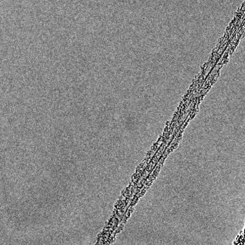
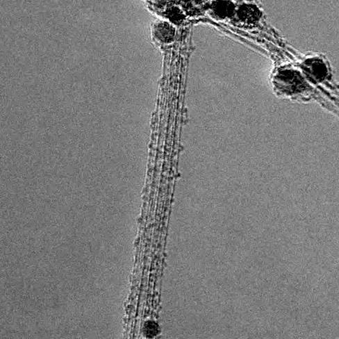
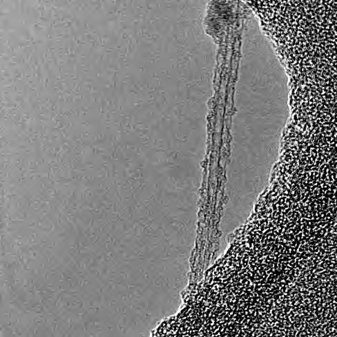
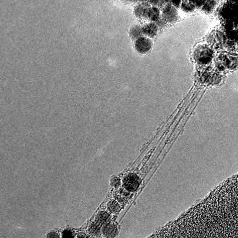
18 Controll of Fullerene density on CNB s via H 2 O increase H 2 O concentration 10nm 10 nm 10nm increase H 2 O concentration 10 nm 10 nm 10 nm 10nm 10 nm


19 0-20 cm 3 /min position in reactor, cm CO 300 cm 3 /min CO 100 cm 3 /min Synthesis of Carbon NanoBuds 885 ºC ferrocene cartridge water cooling circulation 0 particles CNTs and fullerenes µm 945 ºC water nm CO2 or N2 dilutor N 2 12 L/min FT-IR/ ESP Temperature, C 2 nm Filter 0.2 µm A.G.Nasibulin & E.I.Kauppinen et al, Chem.Phys.Lett, 446(2007),

20 NanoBuds TM on FEI Titan TEM at 80kV with image C s -corrector - Movie Individual Fullerene Cluster of Fullerenes Fullerenes are NOT removed by electron beam Image :B.Freitag FEI; samples : Prof. Kauppinen Helsinki, Finnland
21 Frequency Number size distribution of NanoBud TM fullerenes measured from HR-TEM images C C C 34 C C Diameter of fullerenes (nm)
22 Comparison of ultraviolet-visible absorption spectra of CNB s, C 70 and C 60 standards Absorbance (au) Fullerene absortion bands: 4.0 in hexane: in toluene: C 60 C 60 SWCNT absortion bands: 3.5 C 70 C 70 FFCNTs FFCNTs Wavelength (nm)
23 Intensity (au) Raman spectra of NanoBuds carried out by using red (633 nm), green (514 nm), and blue (488 nm) lasers. 2.0x x x x


24 Bonding scenarios of fullerenes on nanotubes based on DFT calculations Calculations By Arkady Krasheninnikov, TKK


25 LT UHV STM: Chemisorbed Fullerene on Nanotube Lattice Ambient STM Peaks in the LDOS are due to nanobuds, cannot be assigned to physisorbed fullerenes Nanometer Range Controll for DOS! Nasibulin & Kauppinen et al. Nature Nanotechnology, 2(3) 156 March 2007


26 Calculations by Arkady Krasheninnikov, TKK Experiment This suggests that chemically attached fullerene via 2+2 cycloaddition is energetically favorable


27 Dry, direct deposition method for Integrated Component Manufacturing Synthesis Process.. CNT Aerosol Deposition Process Products Control of Material Direct Manufacture
28 Traditional CNT film processes are complex Increases cost and may deteriorate performance Produce CNT powder Collect CNT powder Acid purify & sonicate Dirty raw bundled CNTs aerosol or on substrate Chemically purify, functionalize & dry Dirty raw bundled CNTs as powder Filter, spray or spin coat and dry Clean bundled damaged CNTs in liquid Surfactant treat & centrifuge Clean unbundled functionalized damaged CNTs on substrate Surfactant coated unbundled damaged CNTs on substrate Surfactant coated unbundled damaged CNTs in liquid
 2 6 Carbon source: Fe CO + CO = C(s) + CO 2 N 2 12 L/min FT-IR dilutor ESP Moisala, Nasibulin, Brown, Jiang, Khriachtchev, Kauppinen, (2006) Chem. Eng. Sci. 61, 4393.")
29 CO 300 cm 3 /min CO 100 cm 3 /min furnace Experimental set up: Ferrocene Reactor ferrocene cartridge water cooling circulation Catalyst precursor: 85 Ferrocene: 35 Fe(C 24 5 H 5 ) 2 6 Carbon source: Fe CO + CO = C(s) + CO 2 N 2 12 L/min FT-IR dilutor ESP Moisala, Nasibulin, Brown, Jiang, Khriachtchev, Kauppinen, (2006) Chem. Eng. Sci. 61, Filter


30 Small Reactor Large Reactor Flow rate 0.3 liters/min Reactor Tube Diameter Inner 2.5 cm Lentgh 50 cm Flow rate x Small Reactor
 as deposited CNT")

31 SEM images demonstrating CNT film densification by ethanol (b) as deposited CNT film after treatment with ethanol Nasibulin, Ollikainen, Kauppinen et al. Chem. Engin. J. (2008) 136, 409.
 NanoBuds (H2O: 100 ppm) NanoBuds (H2O: 150 ppm) 0 0.0 0.5 1.0 1.5 2.0 2.5 Field strength (V/ m) ACCVD; Tanamura et al.")
32 Cold field emission properties of as-deposited CNB films on Au substrate: comparison with SWCNTs Current density ( A/cm 2 ) SWNTs NanoBuds (H2O: 65 ppm) NanoBuds (H2O: 100 ppm) NanoBuds (H2O: 150 ppm) Field strength (V/ m) ACCVD; Tanamura et al., APL (2006)- SWCNT grown on glass

33 - Large reacto


34 Large reactor tubes - HRTEM at 385C


35 Large reactor tubes - HRTEM at 485C Maria A1 Ethanol treatment heating 485C


36 Large reactor tubes - HRTEM at 485C


37 Dry deposition of CNT networks for TF-FETs Condensation particle counter (CPC) substrate holder 12х12mm Schematic of an ESP substrate size is up to 12х12mm Metal Teflon Metal T.J. Krinke et al., Aerosol Science 33, 2002
![Estimated average density [CNT bundles/um 2 ] CNT](/docs-images/72/66902747/images/38-0.jpg "networks with various densities ρ calc.")


;")
38 Estimated average density [CNT bundles/um 2 ] CNT networks with various densities ρ calc.~12 CNT bundles/µm 2 ρ calc.~8 CNT bundles/µm SiO 2 SiO 2 Cr2 2 AZ Deposition time [min] ρ calc.~5 CNT bundles/µm 2 ρ calc.~2,5 CNT bundles/µm 2 ρ calc.~1 CNT bundles/µm 2 Cr SiO 2 SiO 2 SiO 2 Cr calc. t C Q S ρ-estimated average density (CNTs/µm 2 ); t-time of collection; C-particle concentration by CPC (CNTs/cm 3 ); Q- particle flow (cm 3 /min); S-substrate area (µm 2 ).
")
 on polymer (L=150 µm,")
39 SWCNTN FETs on Si and Kapton substrates on/off`= 10 5, mobility = 5 cm 2 /(V*s) on Si (L=W=50 µm) on/off`= 10 5, mobility = 1cm 2 /(V*s) on polymer (L=150 µm, W=200 µm)

40 THANKS TO YOU FOR YOUR ATTENTION!
Carbon Nanomaterials: Nanotubes and Nanobuds and Graphene towards new products 2030
 Carbon Nanomaterials: Nanotubes and Nanobuds and Graphene towards new products 2030 Prof. Dr. Esko I. Kauppinen Helsinki University of Technology (TKK) Espoo, Finland Forecast Seminar February 13, 2009
Supplementary information for. A Novel Hybrid Carbon Material
 Supplementary information for A Novel Hybrid Carbon Material Albert G. Nasibulin, Peter V. Pikhitsa, Hua Jiang, David P. Brown, Arkady V. Krasheninnikov, Anton S. Anisimov, Paula Queipo, Anna Moisala,
 This article was published in an Elsevier journal. The attached copy is furnished to the author for non-commercial research and education use, including for instruction at the author s institution, sharing
A novel hybrid carbon material
 A novel hybrid carbon material ALBERT G. NASIBULIN 1, PETER V. PIKHITSA 2,HUAJIANG 3, DAVID P. BROWN 1, ARKADY V. KRASHENINNIKOV 4,5, ANTON S. ANISIMOV 1, PAULA QUEIPO 1, ANNA MOISALA 1 *, DAVID GONZALEZ
PHYS-E0541:Special Course in Physics Gas phase synthesis of carbon nanotubes for thin film application. Electron Microscopy. for
 PHYS-E0541:Special Course in Physics Gas phase synthesis of carbon nanotubes for thin film application Electron Microscopy for Introduction to Electron Microscopy Carbon Nanomaterials (nanotubes) Dr. Hua
Introduction to Nanotechnology Chapter 5 Carbon Nanostructures Lecture 1
 Introduction to Nanotechnology Chapter 5 Carbon Nanostructures Lecture 1 ChiiDong Chen Institute of Physics, Academia Sinica chiidong@phys.sinica.edu.tw 02 27896766 Section 5.2.1 Nature of the Carbon Bond
SUPPLEMENTARY INFORMATION
 SUPPLEMENTARY INFORMATION Flexible, high-performance carbon nanotube integrated circuits Dong-ming Sun, Marina Y. Timmermans, Ying Tian, Albert G. Nasibulin, Esko I. Kauppinen, Shigeru Kishimoto, Takashi
In today s lecture, we will cover:
 In today s lecture, we will cover: Metal and Metal oxide Nanoparticles Semiconductor Nanocrystals Carbon Nanotubes 1 Week 2: Nanoparticles Goals for this section Develop an understanding of the physical
Carbon Nanotubes: Development of Nanomaterials for Hydrogen Storage
 Carbon Nanotubes: Development of Nanomaterials for Hydrogen Storage Hongjie Dai Department of Chemistry & Laboratory for Advanced Materials Stanford University GCEP, September 19, 2006 Outline Can carbon
Imaging Carbon materials with correlative Raman-SEM microscopy. Introduction. Raman, SEM and FIB within one chamber. Diamond.
 Imaging Carbon materials with correlative Raman-SEM microscopy Application Example Carbon materials are widely used in many industries for their exceptional properties. Electric conductance, light weight,
Introduction to Nanotechnology Chapter 5 Carbon Nanostructures Lecture 1
 Introduction to Nanotechnology Chapter 5 Carbon Nanostructures Lecture 1 ChiiDong Chen Institute of Physics, Academia Sinica chiidong@phys.sinica.edu.tw 02 27896766 Carbon contains 6 electrons: (1s) 2,
Supported Ni catalysts from nominal monolayer grow single-walled carbon nanotubes.
 Supported Ni catalysts from nominal monolayer grow single-walled carbon nanotubes. Kazunori Kakehi a, Suguru Noda a, *, Shohei Chiashi b, Shigeo Maruyama b a Department of Chemical System Engineering,
2011 GCEP Report. Project title: Self-sorting of Carbon Nanotubes for High Performance Large Area Transparent Electrodes for Solar Cells
 2011 GCEP Report Project title: Self-sorting of Carbon Nanotubes for High Performance Large Area Transparent Electrodes for Solar Cells Investigators Zhenan Bao, Associate Professor, Chemical Engineering
7. Carbon Nanotubes. 1. Overview: Global status market price 2. Types. 3. Properties. 4. Synthesis. MWNT / SWNT zig-zag / armchair / chiral
 7. Carbon Nanotubes 1. Overview: Global status market price 2. Types MWNT / SWNT zig-zag / armchair / chiral 3. Properties electrical others 4. Synthesis arc discharge / laser ablation / CVD 5. Applications
Control of Diameter Distribution of Single-walled Carbon Nanotubes Using the Zeolite-CCVD Method
 22 Special Issue Nano-structure Controls of Functional Powders Research Report Control of Diameter Distribution of Single-walled Carbon Nanotubes Using the Zeolite-CCVD Method Atsuto Okamoto, Hisanori
Carbon Nanotube: The Inside Story
 Krasnoyarsk: 24 th August, 2009 Carbon Nanotube: The Inside Story Review written for Journal of Nanoscience and Nanotechnology Yoshinori ANDO Dean of Faculty of Science and Technology, Meijo University
Nanofabrication/Nano-Characterization Calixarene and CNT Control Technology
 Nanofabrication/Nano-Characterization Calixarene and CNT Control Technology ISHIDA Masahiko, FUJITA Junichi, NARIHIRO Mitsuru, ICHIHASHI Toshinari, NIHEY Fumiyuki, OCHIAI Yukinori Abstract The world of
Investigation on the growth of CNTs from SiO x and Fe 2 O 3 nanoparticles by in situ TEM
 The 5 th Workshop on Nucleation and Growth Mechanisms of SWCNTs Investigation on the growth of CNTs from SiO x and Fe 2 O 3 nanoparticles by in situ TEM Chang Liu Shenyang National Laboratory for Materials
Carbon Nanotubes in Interconnect Applications
 Carbon Nanotubes in Interconnect Applications Page 1 What are Carbon Nanotubes? What are they good for? Why are we interested in them? - Interconnects of the future? Comparison of electrical properties
Carbon Nanotubes for Interconnect Applications Franz Kreupl, Andrew P. Graham, Maik Liebau, Georg S. Duesberg, Robert Seidel, Eugen Unger
 Carbon Nanotubes for Interconnect Applications Franz Kreupl, Andrew P. Graham, Maik Liebau, Georg S. Duesberg, Robert Seidel, Eugen Unger Infineon Technologies Corporate Research Munich, Germany Outline
Wafer-scale fabrication of graphene
 Wafer-scale fabrication of graphene Sten Vollebregt, MSc Delft University of Technology, Delft Institute of Mircosystems and Nanotechnology Delft University of Technology Challenge the future Delft University
Workshop II Nanomaterials Surfaces and Layers Commercialising Carbon Nanotubes
 Workshop II Nanomaterials Surfaces and Layers Commercialising Carbon Nanotubes Harry Swan, Carbon Nanomaterials Business Manager, Thomas Swan & Co. Ltd. Introduction Thomas Swan & Co. Ltd. Carbon Nanotubes
Supporting Information
 Supporting Information Assembly and Densification of Nanowire Arrays via Shrinkage Jaehoon Bang, Jonghyun Choi, Fan Xia, Sun Sang Kwon, Ali Ashraf, Won Il Park, and SungWoo Nam*,, Department of Mechanical
Transport Properties of Novel Carbon Nanotubes and Nanopeapods
 Transport Properties of Novel Carbon Nanotubes and Nanopeapods Takashi Shimada, Yutaka Ohno, Toshiya Okazaki, Toshiki Sugai, Yousuke Nosho, Kazutomo Suenaga, Shigeru Kishimoto, Takashi Mizutani, and Hisanori
Carbon Nanomaterials
 Carbon Nanomaterials STM Image 7 nm AFM Image Fullerenes C 60 was established by mass spectrographic analysis by Kroto and Smalley in 1985 C 60 is called a buckminsterfullerene or buckyball due to resemblance
Supporting Information
 Supporting Information Clustered Ribbed-Nanoneedle Structured Copper Surfaces with High- Efficiency Dropwise Condensation Heat Transfer Performance Jie Zhu, Yuting Luo, Jian Tian, Juan Li and Xuefeng Gao*
Carbon Nanotube Reference Materials and Characterization Jeffrey A. Fagan
 Carbon Nanotube Reference Materials and Characterization Jeffrey A. Fagan National Institute of Standards and Technology Gaithersburg, MD Nanotube Market Composites Energy Electronics Chemical & Engineering
Controlled continuous spinning of fibres of single wall carbon nanotubes
 Controlled continuous spinning of fibres of single wall carbon nanotubes Guadalupe Workshop 8-12 April 2011 Krzysztof Koziol and Alan Windle kk292@cam.ac.uk Department of Materials Science and Metallurgy
What are Carbon Nanotubes? What are they good for? Why are we interested in them?
 Growth and Properties of Multiwalled Carbon Nanotubes What are Carbon Nanotubes? What are they good for? Why are we interested in them? - Interconnects of the future? - our vision Where do we stand - our
SUPPLEMENTARY INFORMATION
 SUPPLEMENTARY INFORMATION Facile Synthesis of High Quality Graphene Nanoribbons Liying Jiao, Xinran Wang, Georgi Diankov, Hailiang Wang & Hongjie Dai* Supplementary Information 1. Photograph of graphene
II.1.4 Nanoengineering of Hybrid Carbon Nanotube-Metal Nanocluster Composite Materials for Hydrogen Storage
 II.1.4 Nanoengineering of Hybrid Carbon Nanotube-Metal Nanocluster Composite Materials for Hydrogen Storage Investigators Kyeongjae (KJ) Cho, Assistant Professor of Mechanical Engineering; Bruce Clemens,
3.3. Nanotubes History and structure History
 3.3. Nanotubes [Own knowledge, Dresselhaus, Dresselhaus and Avouris book, Poole-Owens, Enc. Nanoscience ch. 3] 3.3.1.1. History 3.3.1. History and structure The history of carbon nanotubes is interesting
Supplementary Figure S1. AFM images of GraNRs grown with standard growth process. Each of these pictures show GraNRs prepared independently,
 Supplementary Figure S1. AFM images of GraNRs grown with standard growth process. Each of these pictures show GraNRs prepared independently, suggesting that the results is reproducible. Supplementary Figure
Recap (so far) Low-Dimensional & Boundary Effects
 Low-Dimensional & Boundary Effects") Recap (so far) Ohm s & Fourier s Laws Mobility & Thermal Conductivity Heat Capacity Wiedemann-Franz Relationship Size Effects and Breakdown of Classical Laws 1 Low-Dimensional & Boundary Effects Energy
Recap (so far) Ohm s & Fourier s Laws Mobility & Thermal Conductivity Heat Capacity Wiedemann-Franz Relationship Size Effects and Breakdown of Classical Laws 1 Low-Dimensional & Boundary Effects Energy
There's Plenty of Room at the Bottom
 There's Plenty of Room at the Bottom 12/29/1959 Feynman asked why not put the entire Encyclopedia Britannica (24 volumes) on a pin head (requires atomic scale recording). He proposed to use electron microscope
Supporting Information. Fast Synthesis of High-Performance Graphene by Rapid Thermal Chemical Vapor Deposition
 1 Supporting Information Fast Synthesis of High-Performance Graphene by Rapid Thermal Chemical Vapor Deposition Jaechul Ryu, 1,2, Youngsoo Kim, 4, Dongkwan Won, 1 Nayoung Kim, 1 Jin Sung Park, 1 Eun-Kyu
Supplementary Information
 Electronic Supplementary Material (ESI) for Physical Chemistry Chemical Physics. This journal is the Owner Societies 2015 Supplementary Information Vertical Heterostructures of MoS2 and Graphene Nanoribbons
Nanotechnology in Consumer Products
 Nanotechnology in Consumer Products June 17, 2015 October 31, 2014 The webinar will begin at 1pm Eastern Time Perform an audio check by going to Tools > Audio > Audio Setup Wizard Chat Box Chat Box Send
Spray coating as a simple method to prepare catalyst for growth. of diameter-tunable single-walled carbon nanotubes
 Spray coating as a simple method to prepare catalyst for growth of diameter-tunable single-walled carbon nanotubes Rong Xiang, 1 * Haiqiang Zeng, 1 Yuquan Su, 1 Xuchun Gui, 1 Tianzhun Wu, 1 Erik Einarsson,
Determining Carbon Nanotube Properties from Raman. Scattering Measurements
 Determining Carbon Nanotube Properties from Raman Scattering Measurements Ying Geng 1, David Fang 2, and Lei Sun 3 1 2 3 The Institute of Optics, Electrical and Computer Engineering, Laboratory for Laser
SYNTHESIS OF CARBON NANOTUBES BY CATALYTIC CVD USING Fe-Mo/MgO AND Fe- Mo/Al 2 O 3 CATALYSTS. Abstract. Introduction. Experimental
 SYNTHESIS OF CARBON NANOTUBES BY CATALYTIC CVD USING Fe-Mo/MgO AND Fe- Mo/Al 2 O 3 CATALYSTS Shinn-Shyong Tzeng, Ting-Bin Liang, Sheng-Chuan Wang, Ting-Yu Wu and Yu-Hun Lin Department of Materials Engineering,
Correlation between catalyst particle and single-walled carbon nanotube diameters
 Carbon 43 (2005) 2251 2257 www.elsevier.com/locate/carbon Correlation between catalyst particle and single-walled carbon nanotube diameters Albert G. Nasibulin a, Peter V. Pikhitsa b,1, Hua Jiang c, Esko
Use of Multi-Walled Carbon Nanotubes for UV radiation detection
 Use of Multi-Walled Carbon Nanotubes for UV radiation detection Viviana Carillo 11th Topical Seminar on Innovative Particle and Radiation Detectors (IPRD08) 1-4 October 2008 Siena, Italy A new nanostructured
on Self-Assembly of Fullerene Molecules
 Effect of Surface Preparation of Copper on Self-Assembly of Fullerene Molecules Dongni Ma, Selene Sandoval, Krishna Muralidharan, Srini Raghavan University of Arizona Department of Materials Science and
Template Synthesis of Nano-Structured Carbons
 Template Synthesis of Nano-Structured Carbons Takashi Kyotani Institute of Multidisciplinary Research for Advanced Materials, Tohoku University, JAPAN For controlling complicated carbon structure at nanometer
1. Nanotechnology & nanomaterials -- Functional nanomaterials enabled by nanotechnologies.
 Novel Nano-Engineered Semiconductors for Possible Photon Sources and Detectors NAI-CHANG YEH Department of Physics, California Institute of Technology 1. Nanotechnology & nanomaterials -- Functional nanomaterials
Top down and bottom up fabrication
 Lecture 24 Top down and bottom up fabrication Lithography ( lithos stone / graphein to write) City of words lithograph h (Vito Acconci, 1999) 1930 s lithography press Photolithography d 2( NA) NA=numerical
Novel Tooling for Scaling of High Quality CVD Graphene Production. Karlheinz Strobl, Mathieu Monville, Riju Singhal and Samuel Wright
 Novel Tooling for Scaling of High Quality CVD Graphene Production Karlheinz Strobl, Mathieu Monville, Riju Singhal and Samuel Wright 1 Commercialization of Nano Materials Commercialization Volume production
Initial Stages of Growth of Organic Semiconductors on Graphene
 Initial Stages of Growth of Organic Semiconductors on Graphene Presented by: Manisha Chhikara Supervisor: Prof. Dr. Gvido Bratina University of Nova Gorica Outline Introduction to Graphene Fabrication
Carbon Nanotubes. Andrea Goldoni. Elettra- Sincrotrone Trieste S.C.p.A., s.s. 14 Km 163,5 in Area Science Park, Trieste, Italy
 Carbon Nanotubes Andrea Goldoni Elettra- Sincrotrone Trieste S.C.p.A., s.s. 14 Km 163,5 in Area Science Park, 34012 Trieste, Italy Up to 1985 the only two allotropic form of carbon were known: graphite
SUPPLEMENTARY INFORMATION
 SUPPLEMENTARY INFORMATION Linking catalyst composition to chirality distributions of as-grown singlewalled carbon nanotubes by tuning Ni x Fe 1-x nanoparticles Supplementary Information Wei-Hung Chiang
Overview. Carbon in all its forms. Background & Discovery Fabrication. Important properties. Summary & References. Overview of current research
 Graphene Prepared for Solid State Physics II Pr Dagotto Spring 2009 Laurene Tetard 03/23/09 Overview Carbon in all its forms Background & Discovery Fabrication Important properties Overview of current
Saturable absorbers incorporating carbon nanotubes directly synthesized onto substrates/fibers and their application to mode-locked fiber lasers
 Saturable absorbers incorporating carbon nanotubes directly synthesized onto substrates/fibers and their application to mode-locked fiber lasers S. Yamashita (1), S. Maruyama (2), Y. Murakami (2), Y. Inoue
Supporting Information s for
 Supporting Information s for # Self-assembling of DNA-templated Au Nanoparticles into Nanowires and their enhanced SERS and Catalytic Applications Subrata Kundu* and M. Jayachandran Electrochemical Materials
Multi-Layer Coating of Ultrathin Polymer Films on Nanoparticles of Alumina by a Plasma Treatment
 Mat. Res. Soc. Symp. Vol. 635 2001 Materials Research Society Multi-Layer Coating of Ultrathin Polymer Films on Nanoparticles of Alumina by a Plasma Treatment Donglu Shi, Zhou Yu, S. X. Wang 1, Wim J.
Processing and Properties of Highly Enriched Double-Walled. Carbon Nanotubes: Supplementary Information
 Processing and Properties of Highly Enriched Double-Walled Carbon Nanotubes: Supplementary Information Alexander A. Green and Mark C. Hersam* Department of Materials Science and Engineering and Department
C- Mats and their Applications
 C- Mats and their Applications Materials and Electrochemical Research (MER) Corporation Tucson, Arizona Dr. R. O. LOUTFY MER HISTORY g MER is a private Arizona Corporation started in 1985 by Drs. R.O.Loutfy
Supporting Information
 Electronic Supplementary Material (ESI) for ChemComm. This journal is The Royal Society of Chemistry 2014 Supporting Information Controllable Atmospheric Pressure Growth of Mono-layer, Bi-layer and Tri-layer
Supplementary Figure 1 Experimental setup for crystal growth. Schematic drawing of the experimental setup for C 8 -BTBT crystal growth.
 Supplementary Figure 1 Experimental setup for crystal growth. Schematic drawing of the experimental setup for C 8 -BTBT crystal growth. Supplementary Figure 2 AFM study of the C 8 -BTBT crystal growth
Controlled self-assembly of graphene oxide on a remote aluminum foil
 Supplementary Information Controlled self-assembly of graphene oxide on a remote aluminum foil Kai Feng, Yewen Cao and Peiyi Wu* State key Laboratory of Molecular Engineering of Polymers, Department of
Metallic/semiconducting ratio of carbon nanotubes in a bundle prepared using CVD technique
 PRAMANA c Indian Academy of Sciences Vol. 67, No. 2 journal of August 2006 physics pp. 395 400 Metallic/semiconducting ratio of carbon nanotubes in a bundle prepared using CVD technique KHURSHED AHMAD
Carbon Nanotube Thin-Films & Nanoparticle Assembly
 Nanodevices using Nanomaterials : Carbon Nanotube Thin-Films & Nanoparticle Assembly Seung-Beck Lee Division of Electronics and Computer Engineering & Department of Nanotechnology, Hanyang University,
Seminars in Nanosystems - I
 Seminars in Nanosystems - I Winter Semester 2011/2012 Dr. Emanuela Margapoti Emanuela.Margapoti@wsi.tum.de Dr. Gregor Koblmüller Gregor.Koblmueller@wsi.tum.de Seminar Room at ZNN 1 floor Topics of the
Carbon nanotubes in a nutshell. Graphite band structure. What is a carbon nanotube? Start by considering graphite.
 Carbon nanotubes in a nutshell What is a carbon nanotube? Start by considering graphite. sp 2 bonded carbon. Each atom connected to 3 neighbors w/ 120 degree bond angles. Hybridized π bonding across whole
Understanding Irreducible and Reducible Oxides as Catalysts for Carbon Nanotubes and Graphene Formation
 Wright State University CORE Scholar Special Session 5: Carbon and Oxide Based Nanostructured Materials (2011) Special Session 5 6-2011 Understanding Irreducible and Reducible Oxides as Catalysts for Carbon
CVD growth of Graphene. SPE ACCE presentation Carter Kittrell James M. Tour group September 9 to 11, 2014
 CVD growth of Graphene SPE ACCE presentation Carter Kittrell James M. Tour group September 9 to 11, 2014 Graphene zigzag armchair History 1500: Pencil-Is it made of lead? 1789: Graphite 1987: The first
Measurement of in-plane sheet thermal conductance of single-walled carbon nanotube thin films by steady-state infrared thermography
 Measurement of in-plane sheet thermal conductance of single-walled carbon nanotube thin films by steady-state infrared thermography Ya Feng 1, Taiki Inoue 1, Makoto Watanabe 1, Shuhei Yoshida 1, Yang Qian
Solutions for Assignment-8
 Solutions for Assignment-8 Q1. The process of adding impurities to a pure semiconductor is called: [1] (a) Mixing (b) Doping (c) Diffusing (d) None of the above In semiconductor production, doping intentionally
Nanostrukturphysik. Prof. Yong Lei & Dr. Yang Xu Fachgebiet 3D-Nanostrukturierung, Institut für Physik
 Nanostrukturphysik Prof. Yong Lei & Dr. Yang Xu Fachgebiet 3D-Nanostrukturierung, Institut für Physik Contact: yong.lei@tu-ilmenau.de (3748), yang.xu@tuilmenau.de (4902) Office: Gebäude V202, Unterpörlitzer
Transparent Electrode Applications
 Transparent Electrode Applications LCD Solar Cells Touch Screen Indium Tin Oxide (ITO) Zinc Oxide (ZnO) - High conductivity - High transparency - Resistant to environmental effects - Rare material (Indium)
REDUCED GRAPHITE OXIDE-INDIUM TIN OXIDE COMPOSITES FOR TRANSPARENT ELECTRODE USING SOLUTION PROCESS
 18 TH INTERNATIONAL CONFERENCE ON COMPOSITE MATERIALS REDUCED GRAPHITE OXIDE-INDIUM TIN OXIDE COMPOSITES FOR TRANSPARENT ELECTRODE USING SOLUTION PROCESS K. S. Choi, Y. Park, K-.C. Kwon, J. Kim, C. K.
List of Abbreviations Figure Captions Abstract Introduction Experimental details Results and Discussion...
 Table of Contents List of Abbreviations... 2 Figure Captions... 3 Abstract... 4 1. Introduction... 5 2. Experimental details... 9 3. Results and Discussion... 12 3.1. Microstructural studies of as-prepared
Graphene Fundamentals and Emergent Applications
 Graphene Fundamentals and Emergent Applications Jamie H. Warner Department of Materials University of Oxford Oxford, UK Franziska Schaffel Department of Materials University of Oxford Oxford, UK Alicja
Graphene Novel Material for Nanoelectronics
 Graphene Novel Material for Nanoelectronics Shintaro Sato Naoki Harada Daiyu Kondo Mari Ohfuchi (Manuscript received May 12, 2009) Graphene is a flat monolayer of carbon atoms with a two-dimensional honeycomb
Lattice-Oriented Growth of Single-Walled Carbon Nanotubes
 Letter Subscriber access provided by DUKE UNIV Lattice-Oriented Growth of Single-Walled Carbon Nanotubes Ming Su, Yan Li, Benjamin Maynor, Alper Buldum, Jian Ping Lu, and Jie Liu J. Phys. Chem. B, 2000,
Enhanced photocurrent of ZnO nanorods array sensitized with graphene. quantum dots
 Electronic Supplementary Material (ESI) for RSC Advances. This journal is The Royal Society of Chemistry 2015 Enhanced photocurrent of ZnO nanorods array sensitized with graphene quantum dots Bingjun Yang,
Low Voltage Field Emission SEM (LV FE-SEM): A Promising Imaging Approach for Graphene Samples
: A Promising Imaging Approach for Graphene Samples") Low Voltage Field Emission SEM (LV FE-SEM): A Promising Imaging Approach for Graphene Samples Jining Xie Agilent Technologies May 23 rd, 2012 www.agilent.com/find/nano Outline 1. Introduction 2. Agilent
Low Voltage Field Emission SEM (LV FE-SEM): A Promising Imaging Approach for Graphene Samples Jining Xie Agilent Technologies May 23 rd, 2012 www.agilent.com/find/nano Outline 1. Introduction 2. Agilent
Carbon Engineering Nanocarbon Structures
 Carbon Engineering Nanocarbon Structures Diamond Fullerenes Carbon nanotubes (CNT) multiwalled (MNT) Diamond Like Carbon (DLC) Graphene Nanospheres Allotropes of Carbon Crystalline Diamond Graphite Carbon
Purification and characterization of zeolite-supported single-walled carbon nanotubes catalytically synthesized from ethanol
 Purification and characterization of zeolite-supported single-walled carbon nanotubes catalytically synthesized from ethanol Hideyuki Igarashi, a Hiroto Murakami, a Yoichi Murakami, b Shigeo Maruyama,
Graphene. Tianyu Ye November 30th, 2011
 Graphene Tianyu Ye November 30th, 2011 Outline What is graphene? How to make graphene? (Exfoliation, Epitaxial, CVD) Is it graphene? (Identification methods) Transport properties; Other properties; Applications;
Bratislava, Slovak Republic.
 INTEGRATION OF ATOMIC LAYER DEPOSITED AL 2 O 3 DIELECTRICS WITH GRAPHENE Jana Brndiarová 1, Karol Fröhlich 1, Martin Hulman 1, Alica Rosová 1, Edmund Dobročka 1,Tauno Kahro 2, Jaan Aarik 2 1 Institute
Graphene The Search For Two Dimensions. Christopher Scott Friedline Arizona State University
 Graphene The Search For Two Dimensions Christopher Scott Friedline Arizona State University What Is Graphene? Single atomic layer of graphite arranged in a honeycomb crystal lattice Consists of sp 2 -bonded
In the name of Allah
 In the name of Allah Nano chemistry- 4 th stage Lecture No. 1 History of nanotechnology 16-10-2016 Assistance prof. Dr. Luma Majeed Ahmed lumamajeed2013@gmail.com, luma.ahmed@uokerbala.edu.iq Nano chemistry-4
Engineered Flexible Conductive Barrier Films for Advanced Energy Devices
 The 13 th Korea-U.S. Forum on Nanotechnology Engineered Flexible Conductive Barrier Films for Advanced Energy Devices Jinsung Kwak 1, Yongsu Jo 1, Soon-Dong Park 2, Na Yeon Kim 1, Se-Yang Kim 1, Zonghoon
Nanocarbon Technology for Development of Innovative Devices
 Nanocarbon Technology for Development of Innovative Devices Shintaro Sato Daiyu Kondo Shinichi Hirose Junichi Yamaguchi Graphene, a one-atom-thick honeycomb lattice made of carbon, and a carbon nanotube,
Electronic Supplementary Information. Microwave-assisted, environmentally friendly, one-pot preparation. in electrocatalytic oxidation of methanol
 Electronic Supplementary Information Microwave-assisted, environmentally friendly, one-pot preparation of Pd nanoparticles/graphene nanocomposites and their application in electrocatalytic oxidation of
Toward Clean Suspended CVD Graphene
 Electronic Supplementary Material (ESI) for RSC Advances. This journal is The Royal Society of Chemistry 2016 Supplemental information for Toward Clean Suspended CVD Graphene Alexander Yulaev 1,2,3, Guangjun
Novel Dispersion and Self-Assembly
 Novel Dispersion and Self-Assembly of Carbon Nanotubes Mohammad F. Islam 100g Department of Chemical Engineering and Department of Materials Science & Engineering Funding Agencies http://islamgroup.cheme.cmu.edu
PREPARATION OF LUMINESCENT SILICON NANOPARTICLES BY PHOTOTHERMAL AEROSOL SYNTHESIS FOLLOWED BY ACID ETCHING
 Phase Transitions Vol. 77, Nos. 1 2, January February 2004, pp. 131 137 PREPARATION OF LUMINESCENT SILICON NANOPARTICLES BY PHOTOTHERMAL AEROSOL SYNTHESIS FOLLOWED BY ACID ETCHING X. LI, Y. HE, S.S. TALUKDAR
Supplementary Figure 1. Electron micrographs of graphene and converted h-bn. (a) Low magnification STEM-ADF images of the graphene sample before
 Low magnification STEM-ADF images of the graphene sample before") Supplementary Figure 1. Electron micrographs of graphene and converted h-bn. (a) Low magnification STEM-ADF images of the graphene sample before conversion. Most of the graphene sample was folded after
Supplementary Figure 1. Electron micrographs of graphene and converted h-bn. (a) Low magnification STEM-ADF images of the graphene sample before conversion. Most of the graphene sample was folded after
EN2912C: Future Directions in Computing Lecture 08: Overview of Near-Term Emerging Computing Technologies
 EN2912C: Future Directions in Computing Lecture 08: Overview of Near-Term Emerging Computing Technologies Prof. Sherief Reda Division of Engineering Brown University Fall 2008 1 Near-term emerging computing
3D Boron doped Carbon Nanorods/Carbon-Microfiber Hybrid Composites: Synthesis and Applications as Highly Stable Proton Exchange Membrane Fuel Cell
 Electronic Supplementary Information for Journal of Materials Chemistry 3D Boron doped Carbon Nanorods/Carbon-Microfiber Hybrid Composites: Synthesis and Applications as Highly Stable Proton Exchange Membrane
Diameter-Controlled Growth of Carbon Nanotubes
 106 Chapter 6: Microdischarge Synthesis of Fe Nanoparticles for Diameter-Controlled Growth of Carbon Nanotubes 6.1. Introduction Nanometer-sized materials represent the future building blocks of nanoscale
2 nd Workshop on Nanoscience: Carbon-Related Systems and Nanomaterials July 3-7, 2012, NCKU, Tainan, Taiwan
 2 nd Workshop on Nanoscience: Carbon-Related Systems and Nanomaterials July 3-7, 2012, NCKU, Tainan, Taiwan Reorganization of sp 2 carbon, and the tubule growth Synthesis of nano-carbon materials Carbon
Nanoscale thermal transport and the thermal conductance of interfaces
 Nanoscale thermal transport and the thermal conductance of interfaces David G. Cahill Scott Huxtable, Zhenbin Ge, Paul Bruan Materials Research Laboratory and Department of Materials Science Zhaohui Wang,
2D Materials for Gas Sensing
 2D Materials for Gas Sensing S. Guo, A. Rani, and M.E. Zaghloul Department of Electrical and Computer Engineering The George Washington University, Washington DC 20052 Outline Background Structures of
NEM Relays Using 2-Dimensional Nanomaterials for Low Energy Contacts
 NEM Relays Using 2-Dimensional Nanomaterials for Low Energy Contacts Seunghyun Lee, Ji Cao 10/29/2013 A Science & Technology Professor H. -S. Philip Wong Electrical Engineering, Stanford University Center
Stretchable Graphene Transistors with Printed Dielectrics and Gate Electrodes
 Stretchable Graphene Transistors with Printed Dielectrics and Gate Electrodes Seoung-Ki Lee, Beom Joon Kim, Houk Jang, Sung Cheol Yoon, Changjin Lee, Byung Hee Hong, John A. Rogers, Jeong Ho Cho, Jong-Hyun
Carbon nanotubes synthesis. Ing. Eva Košťáková KNT, FT, TUL
 Carbon nanotubes synthesis Ing. Eva Košťáková KNT, FT, TUL Basic parameters: -Temperature (500, 1000 C ) -Pressure (normal, vacuum ) -Gas (ambient, inert atmosphere nitrogen, argon ) -Time (duration, time
Carbon nanotubes in a nutshell
 Carbon nanotubes in a nutshell What is a carbon nanotube? Start by considering graphite. sp 2 bonded carbon. Each atom connected to 3 neighbors w/ 120 degree bond angles. Hybridized π bonding across whole