Lecture 5, Part 2: Novel functionalities of chalcogenide glasses
|
|
|
- Sarah Owen
- 5 years ago
- Views:
Transcription

1 Lehigh University Lehigh Preserve US-Japan Winter School Semester Length Glass Courses and Glass Schools Winter Lecture 5, Part 2: Novel functionalities of chalcogenide glasses Himanshu Jain Lehigh University Follow this and additional works at: Part of the Materials Science and Engineering Commons Recommended Citation Jain, Himanshu, "Lecture 5, Part 2: Novel functionalities of chalcogenide glasses" (2008). US-Japan Winter School This Video is brought to you for free and open access by the Semester Length Glass Courses and Glass Schools at Lehigh Preserve. It has been accepted for inclusion in US-Japan Winter School by an authorized administrator of Lehigh Preserve. For more information, please contact
2 Novel functionalities of chalcogenide glasses Himanshu Jain Dept. of Materials Science & Engineering Lehigh University, Bethlehem, PA Thanks to. G. Chen, A. Ganjoo, K. Antoine, I. Biaggio Lehigh University National Science Foundation International Materials Institute for New Functionality in Glass 1 US-Japan Winter School Jain.01 08

3 2 US-Japan Winter School Jain.01 08
 sensitive to bandgap light (1 T g ( C) 3 ev), e-beam, x-rays Silicates ~ 700 As-Se ~ 150 photosensitive (photodarkening & photoexpansion) Compounds of S, Se and Te e.g. elemental Se, Ge-Se, As-Se, As-S, Sb-Te, 3 US-Japan Winter School Jain.")
4 What are Chalcogenide Glasses? After I.D. Aggarwal, J.S. Sanghera, Development and Applications of Chalcogenide Glass Fibers at NRL transmission in the infrared high refractive index (~ ) sensitive to bandgap light (1 T g ( C) 3 ev), e-beam, x-rays Silicates ~ 700 As-Se ~ 150 photosensitive (photodarkening & photoexpansion) Compounds of S, Se and Te e.g. elemental Se, Ge-Se, As-Se, As-S, Sb-Te, 3 US-Japan Winter School Jain.01 08
 Laser")


5 Recent new functionalities: CD-RW and DVD-RW: Phase-change memory b) Laser power controls the switching between amorphous and crystalline states. DVD-RW High power Medium power amorphous crystalline 5 US-Japan Winter School Jain.01 08

6 6 US-Japan Winter School Jain.01 08

7 7 US-Japan Winter School Jain.01 08

8 8 US-Japan Winter School Jain.01 08


9 Crystal structure of As 2 Se 3 Se Se Se Se Se Se Two-dimensional layer structure Se Se Se Se Se Se Se Covalent bonding: 8-N rule Se: 2-fold As: 3-fold Each As bonds to Se Each Se bonds to As 9 US-Japan Winter School Jain.01 08
10 S As Crystalline structure of As 2 S 3 Layered structure Covalent bonding: S: 2-fold2 As: 3-fold3 Each As bonds to S Each S bonds to As Layer 1 Layer 2 10 US-Japan Winter School Jain As S (Se)

11 Se Ge Crystalline structure of GeSe 2 3D Four fold coordinated Covalent bonding: Se: 2-fold2 Ge: 4-fold4 Each Ge bonds to Se Each Se bonds to Ge Corner Sharing Edge Sharing 11 US-Japan Winter School Jain.01 08
: 2 Se 20 Se 3+ + Se 1 - Li and Drabold (2001) Chemical disorder Coordination defects As High Low Se High High 12 US-Japan Winter School Jain.")
12 First Principles MD simulation of a-as 2 Se 3 structure Se atom As atom VAP Chemical disorder: As-As and Se-Se Coordination defects: Se 3+, Se 1-, As 4+, As 2 - Valence alternation pairs (VAP): 2 Se 20 Se 3+ + Se 1 - Li and Drabold (2001) Chemical disorder Coordination defects As High Low Se High High 12 US-Japan Winter School Jain.01 08
 Convex and concave structures can be developed by light on changing the composition What happens at the atomic scale? Can we see similar features at an atomic scale?")
13 Wide composition range As based films expand and photodarken Ge- based films contract and photo bleach Potential new applications: Creating micro and nano-sized optical components (lenses, gratings etc.) Convex and concave structures can be developed by light on changing the composition What happens at the atomic scale? Can we see similar features at an atomic scale?? * Kuzukawa, Ganjoo and Shimakawa; J. Non-Cryst. Solids (1998) 13 US-Japan Winter School Jain.01 08
14 Temporary reversible effects 15 photodarkening photoexpansion Δα (cm -1 )x Δd/d (%) OFF ON Time (s) Change in absorptivity with time for a-as 2 Se 3 films, Δα, after illumination at 50 K (solid line) and 300 K (dashed line). Ar laser ON and OFF for 20 s each at 50 K; and 10/20 s at 300 K. (Ganjoo et al.) 14 US-Japan Winter School Jain.01 08
15 Photostructuring of ChG: Why ChG? Based on group VI elements (S, Se, Te) as one of the major components. e.g. Se, sulfides or selenides of Ge, Sb or As, etc. Materials that may show photosensitivity have: Low average coordination number ]Also favor glass formation Low steric hindrance or large internal volume Strong localization of light generated e-h pair: tight binding, lack of periodicity / disorder Concentration of recombination energy in a small volume and change in valence of atoms before recombination. Chalcogenide glasses are best suited for producing photosensitive phenomena by the near and abovebandgap-light illumination. 15 US-Japan Winter School Jain Bandgap light Excitation Conduction band Valence band Recombination
16 Consequence of photostructuring What does it do? Miracles volume: integrated optics devices amorphization/ devitrification: CD-RW, DVD-RW mechanical properties - plasticity viscosity - athermal melting optical properties - darkening, birefringence electrical properties - conductivity, dielectric constant chemical properties - etching, dissolution 16 US-Japan Winter School Jain.01 08

17 17 US-Japan Winter School Jain.01 08
18 Classification Photoinduced Changes Ability to recover Effect of light polarization Permanent Reversible Scalar Vector Metastable Temporary Permanent: can't be recovered w/o remaking the glass Metastable: recovered on heating to ~Tg Temporary: recovered on removing the light Scalar: don t depend upon the polarization of the light Vector: depend upon the polarization of the light 18 US-Japan Winter School Jain Temporary + Vector = Smart

19 19 US-Japan Winter School Jain.01 08

20 20 US-Japan Winter School Jain.01 08
21 Distribution of coordination configurations for Se in a-as 2 Se 3 ON AF OFF Laser irrad. 30MIN Se-[2(Se/As)] 70.0% 60.0% CN = 2 Se-[3(Se/As)] Se-(Se) Permanent 50.0% Total Number 40.0% 30.0% 20.0% 10.0% CN = 1 CN = 3 Laser reduces coordination defects around Se permanently Optical annealing 0.0% AF 30MIN ON OFF 22 US-Japan Winter School Jain.01 08
22 X-ray absorption fine structure (XAFS) What can we obtain from EXAFS? Local structure around a specific element. Average inter atomic distance (R) Mean square relative displacement (MSRD) average coordination number (CN) X-rays of varying photon energies excite the electrons in a central atom (absorbed=> absorption edge) Resulting photoelectrons have a low kinetic energy and are backscattered by the atoms surrounding the emitting atom. Probability of backscattering depends on the energy of the photoelectrons. The net result is a series of oscillations on the high photon energy side of the absorption edge. Absorption (a.u) NEXAFS EXAFS Se K-edge X-ray energy (kev) XAFS spectrum of Se K-edge Honorary Symposium Recognizing the Life Long Contributions of Professor Cornelius T. Moynihan Structure and Properties of Non-Oxide Glasses
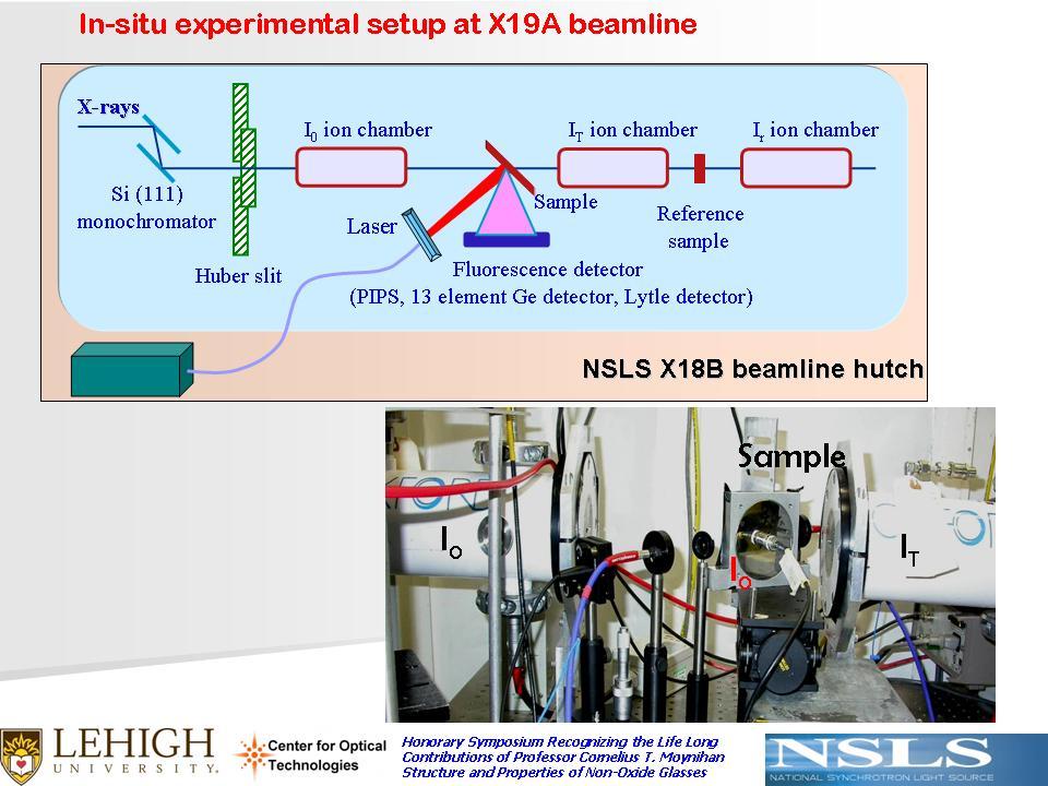
23 Experimental details a-as 2 S 3 films; a-gese 2 films In-situ EXAFS at NSLS, BNL For a-as 2 S 3 films: beamline X19A; As ( kev) and S (2.472 kev) K-edges (Different spots, different scans) For a-gese 2 films: beamline X18B; Ge ( kev) and Se( kev) K-edges (Same spot; one scan) Data collected in fluorescence mode before (As prepared: AP), during (ON) and after laser illumination (OFF) states of the sample Illumination sources For a-as 2 S 3 films: Ar + laser (488 nm; 50 mw/cm 2 ) For a-gese 2 films: Semiconductor laser (633 nm; 50 mw/cm 2 )
24

25 In situ EXAFS Synchrotron x-rays: linearly polarized Looking for laser-induced polarization-dependent changes. 26 US-Japan Winter School Jain.01 08
26 (a): X-ray absorption spectrum of an a-as 40 Se 60 film beyond As and Se K-edges. (b) and (c): The EXAFS oscillations derived from (a). χ(k) (arb. unit) Absorption (arb. unit) EXAFS Spectra As As Se Wave number k (Å -1 ) (b) Energy (kev) χ(k) (arb. unit) Se (a) (c) Wave number k (Å -1 ) 27 US-Japan Winter School Jain.01 08
27 Structural changes around As atoms Sample: as-prepared As 40 Se 60 film As 5.0 As R (Å) VP HP AP ON OFF Sample stages MSRD (10-3 Å 2 ) VP HP AP ON OFF Sample stages AP: as-prepared ON: laser is on OFF: laser is off VP: laser has vertical polarization. HP: laser has horizontal polarization X-rays polarization is horizontal. 28 US-Japan Winter School Jain.01 08
28 Structural changes around Se atoms Sample: as-prepared As 40 Se 60 film R (Å) Se VP HP AP ON OFF AP: as-prepared ON: laser is on OFF: laser is off Sample stages MSRD (10-3 Å 2 ) 5.2 Se VP HP AP ON OFF Sample stages VP: laser has vertical polarization. HP: laser has horizontal polarization X-rays polarization is horizontal. 29 US-Japan Winter School Jain.01 08
29 Mechanisms of Scalar Changes R As-NN : small permanent expansion R Se-NN : large permanent expansion 1. Photo-chemical reaction Covalent Radii: Microscopic heterogeneity in AP films As: 1.21 Å. Se: 1.17 Å Light Se Se + As As 2As Se R As-As > R As-Se > R Se-Se R Se-NN and R As-NN However, experiments: in both R Se-NN and R As-NN As Se As Se 30 US-Japan Winter School Jain.01 08
30 2. Strain relief Intramolecular bonds in As-rich molecules are highly strained breaking of such molecules by light will R As-Se R Se-NN and R As-NN large in R Se-NN & small in R As-NN 31 US-Japan Winter School Jain.01 08
31 PRDF around Ge for a-gesea 2 films FT (χ(k)xk 3 ) (x10-1 ) (a.u) Ge FT (χ(k)xk 3 ) (x10-1 ) (a.u) R (Å) R (Å) As deposited film During Illumination After Illumination 32 US-Japan Winter School Jain.01 08
32 GeSe 2 EXAFS Ge NN Se NN R (Å) AP ON OFF Sample state MSRD (x10-3 ) (Å 2 ) Ge NN Se NN AP ON OFF Sample state 33 US-Japan Winter School Jain.01 08
 Ge-Se bonds energetically favored Bond lengths from covalent radii: Ge-Ge (2.44 Å) ) > Ge-Se (2.36 Å) ) > Se-Se (2.")
33 a-gese 2 films: Decrease in Ge NN and Se NN distances with illumination CONTRACTION IN VOLUME Se Mechanism of photoinduced changes AP films: Chemical disorder: Ge-Se, Ge-Ge and Se-Se bonds 1. Photochemical reaction Ge Ge + Se Se 2 Ge Se (similar to effect of annealing) Ge-Se bonds energetically favored Bond lengths from covalent radii: Ge-Ge (2.44 Å) ) > Ge-Se (2.36 Å) ) > Se-Se (2.32 Å) R Ge-NN should decrease and R Se-NN should increase; but R Se-NN is also decreasing 2. Strain relief Light has similar effect on the NN distance as thermal annealing does Light relieves highly strained atoms (mostly strained 2 fold Se atoms bonded both to Ge and Se) Decrease in Se NN distances - Experimentally observed by in-situ EXAFS Ge Se Ge 34 US-Japan Winter School Jain.01 08
34 Mechanism of photo-structural change LP MD simulation shows Se 4p lone pair (LP) electrons occupy top of the valence band Li, Drabold, et al. (2003) 35 US-Japan Winter School Jain.01 08
35 Mechanism of Vectoral Changes LP Li, Drabold, et al. (2003) MD simulation shows Se 4p lone pair (LP) electrons occupy top of the valence band AP: As-rich molecules (As 4 Se 4 ) and Se-rich phase co-exist in AP a-as 2 Se 3 film. ON: As dangling bonds (from As-As bonds in As 4 Se 4 molecules) react with preferentially excited Se 4p LP s (orbital // E laser ), form anisotropic As-Se. OFF: Anisotropic As-Se bonds can be detected by polarized X-rays. 36 US-Japan Winter School Jain.01 08
36 Amorphous Semiconductors Excited electronic carriers Relaxation Within ps region, electrons relax to the bottom of conduction band (sometimes forming polarons) System Equilibrium mainly through: Electronic relaxations and lattice relaxations Carriers recombine radiatively or non-radiatively, and the electronic relaxation terminates In capture process (trapping and detrapping) lattice distortion may be enhanced Lattice relaxations may occur in time domain extending from ~ps to infinite times energy Energy-relaxation processes in amorphous semiconductors Electronic A B C Lattice time (s) A: Non-radiative recombination B: Radiative recombination C: Capturing process 37 US-Japan Winter School Jain Ke. Tanaka, JAP (1989)
 Measurements after illumination (Metastable state only) In-situ measurements at a single wavelength should represent changes at other wavelengths as well? Tanaka et. al.")
37 Photoinduced changes in absorption coefficient Absorption edge believed to shift in parallel by annealing and illumination (Tanaka et. al., 1981) Measurements after illumination (Metastable state only) In-situ measurements at a single wavelength should represent changes at other wavelengths as well? Tanaka et. al., JNCS (1981) 38 US-Japan Winter School Jain.01 08
38 Speed of reversibility is crucial: In situ vis-nir spectroscopy Use of an optical spectrometer ( nm) that allows real time data acquisition in the millisecond range. Neutral density filter Probe iris iris a-as 2 Se 3 film on glass substrate Detector Beam expander Light from probe beam and pump beam are coincident on the film. Probe beam size is smaller than pump beam Pump laser 660 nm computer 39 US-Japan Winter School Jain.01 08
39 40 US-Japan Winter School Jain.01 08
40 PD kinetics in the strong absorption region ( 10 4 cm -1 ) Transmission (%) Optical transmission spectra of a-as 2 Se 3 film Pump laser λ = 660 nm I 0 = 280 mw/cm 2 Strong absorption region (α 10 4 cm -1 ) US-Japan Winter School Jain Wavelength (nm)
41 Photobleaching in Ge-Se glass 42 US-Japan Winter School Jain.01 08

][1 - exp(-t/τ) β ] Ganjoo")
 43 US-Japan")
42 Evolution of photodarkening λ=633 nm Initial photodarkening: As 2 S 3 :λ pump =488 nm, I 0 =25mW/cm 2 Δα =[α - α(t=0)][1 - exp(-t/τ) β ] Ganjoo and Jain, Phys. Rev. B 74, (2006) 43 US-Japan Winter School Jain.01 08
43 Photodarkening kinetics at various intensities Plot of Δα(I 0 ) vs. t for λ = 600 nm. I 0 = laser intensity. Δα (cm -1 ) 2.0x x x x x x x x x x x a-as 2 Se 3 under in situ illumination Time evolution of Δα(I nm Pump laser λ = 660 nm Time (sec) I 0 = 30 mw/cm 2 I 0 = 94 mw/cm 2 I 0 = 187 mw/cm 2 I 0 = 280 mw/cm 2 44 US-Japan Winter School Jain.01 08
44 Plot of τ vs. I 0 τ (sec) nm 610nm 620nm a-as 2 Se 3 under in situ illumination Pump laser λ = 660 nm Stretched exponential: Δα = [α α(t=0)][1-exp(-t/τ) β ] US-Japan Winter School Jain Intensity, I 0 (mw/cm 2 )
45 Fast optical changes Decay of the transient part of photoinduced changes in transmission with time after pulsed laser illumination (1.1 mj/cm 2 ) Sakaguchi and Tamura, Journal of Physics: Condensed Matter (2006) 46 US-Japan Winter School Jain.01 08

46 Fast photo-effects by transient grating method 47 US-Japan Winter School Jain CW probe Two nearly equal intensity laser pulses made to cross within the sample at an angle Interference of two writing pulses within the sample writes a transient grating (by inducing a change in the refractive index) The grating spacing varies with angle between the writing beams. The refractive index grating is read by diffracting a probe beam off the grating at the Bragg condition The diffracted probe light is collected by a high speed photomultiplier As grating disappears, the time dependence of the probe intensity reflects the decay of the change in refractive index and thus the carrier kinetics
47 Advantages of transient grating technique Λ 1 θ Sample θ High signal/noise ratio Can control the grating spacing (e.g , 1.1 and 1.65 μm presently) by changing the angle between the two beams Helpful in understanding the meaning of the time constants 48 US-Japan Winter School Jain.01 08
48 Ultra fast photoinduced changes from 20 ps pulse Transient Grating, Four- Wave Mixing method: diffracted intensity Intensity (a.u.) Peak intensity (a.u.) Power (mj) Time (ns) The photo-response to pulsed illumination is composed of a fast ~80 ps component followed by nanosecond component. The ultra fast component shows almost thirdorder power dependence indicating third-order nonlinear effect in As50Se US-Japan Winter School Jain.01 08
49 Grating spacing: 1.65 μm Amplitude (a.u.) 5.0x x x x x x x x x x10-4 Amplitude (a.u.) 5.0x x x x x time (μs) 0.72 mj/cm mj/cm mj/cm 2 Δn n ~1.21x x US-Japan Winter School Jain time (μs)
50 mj/cm mj/cm mj/cm 2 Square fit τ (sec) x x10-6 2x10⁻⁶ Grating Spacing (Λ) (m) 2 Λ τ Relaxation time varies as square of grating spacing nearly independent on the power density of the pump (in the range studied) 51 US-Japan Winter School Jain.01 08
Observation of nanosecond light induced thermally tunable transient dual absorption bands in a-ge 5 As 30 Se 65 thin film
 Observation of nanosecond light induced thermally tunable transient dual absorption bands in a-ge 5 As 30 Se 65 thin film Pritam Khan, Tarun Saxena and K.V. Adarsh Department of Physics, Indian Institute
CHALCOGENIDE GLASSES: TRANSFORMATION AND CHANGE. Stephen Elliott Department of Chemistry University of Cambridge.
 CHALCOGENIDE GLASSES: TRANSFORMATION AND CHANGE Stephen Elliott Department of Chemistry University of Cambridge sre1@cam.ac.uk Chalcogenide Advanced Manufacturing Partnership (ChAMP): March 9, 2015 Chalcogenides
Optical and Photonic Glasses. Lecture 30. Femtosecond Laser Irradiation and Acoustooptic. Professor Rui Almeida
 Optical and Photonic Glasses : Femtosecond Laser Irradiation and Acoustooptic Effects Professor Rui Almeida International Materials Institute For New Functionality in Glass Lehigh University Femto second
Photonics applications II. Ion-doped ChGs
 Photonics applications II Ion-doped ChGs 1 ChG as a host for doping; pros and cons - Important - Condensed summary Low phonon energy; Enabling emission at longer wavelengths Reduced nonradiative multiphonon
An Introduction to Diffraction and Scattering. School of Chemistry The University of Sydney
 An Introduction to Diffraction and Scattering Brendan J. Kennedy School of Chemistry The University of Sydney 1) Strong forces 2) Weak forces Types of Forces 3) Electromagnetic forces 4) Gravity Types
Solid State Spectroscopy Problem Set 7
 Solid State Spectroscopy Problem Set 7 Due date: June 29th, 2015 Problem 5.1 EXAFS Study of Mn/Fe substitution in Y(Mn 1-x Fe x ) 2 O 5 From article «EXAFS, XANES, and DFT study of the mixed-valence compound
Re-writable DVDs: what makes phase-change materials work the way they do
 Re-writable DVDs: what makes phase-change materials work the way they do A.V. Kolobov 1,2, P. Fons 1, J. Tominaga 2 1 Center for Applied Near-Field Optics Research, National Institute of Advanced Industrial
Investigation of Optical Nonlinearities and Carrier Dynamics in In-Rich InGaN Alloys
 Vol. 113 (2008) ACTA PHYSICA POLONICA A No. 3 Proceedings of the 13th International Symposium UFPS, Vilnius, Lithuania 2007 Investigation of Optical Nonlinearities and Carrier Dynamics in In-Rich InGaN
X-ray Spectroscopy. Interaction of X-rays with matter XANES and EXAFS XANES analysis Pre-edge analysis EXAFS analysis
 X-ray Spectroscopy Interaction of X-rays with matter XANES and EXAFS XANES analysis Pre-edge analysis EXAFS analysis Element specific Sensitive to low concentrations (0.01-0.1 %) Why XAS? Applicable under
Intensity / a.u. 2 theta / deg. MAPbI 3. 1:1 MaPbI 3-x. Cl x 3:1. Supplementary figures
 Intensity / a.u. Supplementary figures 110 MAPbI 3 1:1 MaPbI 3-x Cl x 3:1 220 330 0 10 15 20 25 30 35 40 45 2 theta / deg Supplementary Fig. 1 X-ray Diffraction (XRD) patterns of MAPbI3 and MAPbI 3-x Cl
X-ray Absorption Spectroscopy. Kishan K. Sinha Department of Physics and Astronomy University of Nebraska-Lincoln
 X-ray Absorption Spectroscopy Kishan K. Sinha Department of Physics and Astronomy University of Nebraska-Lincoln Interaction of X-rays with matter Incident X-ray beam Fluorescent X-rays (XRF) Scattered
An Introduction to XAFS
 An Introduction to XAFS Matthew Newville Center for Advanced Radiation Sources The University of Chicago 21-July-2018 Slides for this talk: https://tinyurl.com/larch2018 https://millenia.cars.aps.anl.gov/gsecars/data/larch/2018workshop
4. Other diffraction techniques
 4. Other diffraction techniques 4.1 Reflection High Energy Electron Diffraction (RHEED) Setup: - Grazing-incidence high energy electron beam (3-5 kev: MEED,
Mechanisms of Visible Photoluminescence from Size-Controlled Silicon Nanoparticles
 Mat. Res. Soc. Symp. Proc. Vol. 737 23 Materials Research Society F1.5.1 Mechanisms of Visible Photoluminescence from Size-Controlled Silicon Nanoparticles Toshiharu Makino *, Nobuyasu Suzuki, Yuka Yamada,
On the reversible photo-darkening in amorphous Ge 5 As 41 S 15 Se 39 film
 JOURNAL OF OPTOELECTRONICS AND ADVANCED MATERIALS Vol. 8, No. 2, April 26, p. 78-784 On the reversible photo-darkening in amorphous Ge 5 As 41 S 15 Se 39 film M. KINCL, K. PETKOV a, L. TICHY * Joint Laboratory
2008,, Jan 7 All-Paid US-Japan Winter School on New Functionalities in Glass. Controlling Light with Nonlinear Optical Glasses and Plasmonic Glasses
 2008,, Jan 7 All-Paid US-Japan Winter School on New Functionalities in Glass Photonic Glass Controlling Light with Nonlinear Optical Glasses and Plasmonic Glasses Takumi FUJIWARA Tohoku University Department
Visualization of Xe and Sn Atoms Generated from Laser-Produced Plasma for EUV Light Source
 3rd International EUVL Symposium NOVEMBER 1-4, 2004 Miyazaki, Japan Visualization of Xe and Sn Atoms Generated from Laser-Produced Plasma for EUV Light Source H. Tanaka, A. Matsumoto, K. Akinaga, A. Takahashi
Femtosecond laser microfabrication in. Prof. Dr. Cleber R. Mendonca
 Femtosecond laser microfabrication in polymers Prof. Dr. Cleber R. Mendonca laser microfabrication focus laser beam on material s surface laser microfabrication laser microfabrication laser microfabrication
Methods of surface analysis
 Methods of surface analysis Nanomaterials characterisation I RNDr. Věra Vodičková, PhD. Surface of solid matter: last monoatomic layer + absorbed monolayer physical properties are effected (crystal lattice
Photonics applications 5: photoresists
 IMI-NFG s Mini Course on Chalcogenide Glasses Lecture 11 Photonics applications 5: photoresists Himanshu Jain Department of Materials Science & Engineering Lehigh University, Bethlehem, PA 18015 H.Jain@Lehigh.edu
Supplementary Figure 1
 Supplementary Figure 1 XRD patterns and TEM image of the SrNbO 3 film grown on LaAlO 3(001) substrate. The film was deposited under oxygen partial pressure of 5 10-6 Torr. (a) θ-2θ scan, where * indicates
Supporting Information s for
 Supporting Information s for # Self-assembling of DNA-templated Au Nanoparticles into Nanowires and their enhanced SERS and Catalytic Applications Subrata Kundu* and M. Jayachandran Electrochemical Materials
Introduction to XAFS. Grant Bunker Associate Professor, Physics Illinois Institute of Technology. Revised 4/11/97
 Introduction to XAFS Grant Bunker Associate Professor, Physics Illinois Institute of Technology Revised 4/11/97 2 tutorial.nb Outline Overview of Tutorial 1: Overview of XAFS 2: Basic Experimental design
Q. Shen 1,2) and T. Toyoda 1,2)
 and T. Toyoda 1,2)") Photosensitization of nanostructured TiO 2 electrodes with CdSe quntum dots: effects of microstructure in substrates Q. Shen 1,2) and T. Toyoda 1,2) Department of Applied Physics and Chemistry 1), and
Photosensitization of nanostructured TiO 2 electrodes with CdSe quntum dots: effects of microstructure in substrates Q. Shen 1,2) and T. Toyoda 1,2) Department of Applied Physics and Chemistry 1), and
X-ray Absorption Spectroscopy
 X-ray Absorption Spectroscopy Matthew Newville Center for Advanced Radiation Sources University of Chicago 12-Sept-2014 SES VI SES VI 12-Sept-2014 SES VI What Is XAFS? X-ray Absorption Fine-Structure (XAFS)
PHOTOCURRENT RELAXATION IN As x Se 1-x THIN FILMS: COMPOSITIONAL DEPENDENCE
 Journal of Optoelectronics and Advanced Materials Vol. 7, No. 5, October 2005, p. 2317-2322 PHOTOCURRENT RELAXATION IN As x Se 1-x THIN FILMS: COMPOSITIONAL DEPENDENCE M. S. Iovu, I. A. Vasiliev, D. V.
(b) Spontaneous emission. Absorption, spontaneous (random photon) emission and stimulated emission.
 Spontaneous emission. Absorption, spontaneous (random photon) emission and stimulated emission.") Lecture 10 Stimulated Emission Devices Lasers Stimulated emission and light amplification Einstein coefficients Optical fiber amplifiers Gas laser and He-Ne Laser The output spectrum of a gas laser Laser
Lecture 10 Stimulated Emission Devices Lasers Stimulated emission and light amplification Einstein coefficients Optical fiber amplifiers Gas laser and He-Ne Laser The output spectrum of a gas laser Laser
Surface Characte i r i zat on LEED Photoemission Phot Linear optics
 Surface Characterization i LEED Photoemission Linear optics Surface characterization with electrons MPS M.P. Seah, WA W.A. Dench, Surf. Interf. Anal. 1 (1979) 2 LEED low energy electron diffraction De
(002)(110) (004)(220) (222) (112) (211) (202) (200) * * 2θ (degree)
(110) (004)(220) (222) (112) (211) (202) (200) * * 2θ (degree)") Supplementary Figures. (002)(110) Tetragonal I4/mcm Intensity (a.u) (004)(220) 10 (112) (211) (202) 20 Supplementary Figure 1. X-ray diffraction (XRD) pattern of the sample. The XRD characterization indicates
Supplementary Figures. (002)(110) Tetragonal I4/mcm Intensity (a.u) (004)(220) 10 (112) (211) (202) 20 Supplementary Figure 1. X-ray diffraction (XRD) pattern of the sample. The XRD characterization indicates
Supplementary Materials
 Supplementary Materials Sample characterization The presence of Si-QDs is established by Transmission Electron Microscopy (TEM), by which the average QD diameter of d QD 2.2 ± 0.5 nm has been determined
Imaging Methods: Scanning Force Microscopy (SFM / AFM)
") Imaging Methods: Scanning Force Microscopy (SFM / AFM) The atomic force microscope (AFM) probes the surface of a sample with a sharp tip, a couple of microns long and often less than 100 Å in diameter.
Imaging Methods: Scanning Force Microscopy (SFM / AFM) The atomic force microscope (AFM) probes the surface of a sample with a sharp tip, a couple of microns long and often less than 100 Å in diameter.
Semiconductor physics I. The Crystal Structure of Solids
 Lecture 3 Semiconductor physics I The Crystal Structure of Solids 1 Semiconductor materials Types of solids Space lattices Atomic Bonding Imperfection and doping in SOLIDS 2 Semiconductor Semiconductors
Microfabricação em materiais poliméricos usando laser de femtossegundos
 Microfabricação em materiais poliméricos usando laser de femtossegundos Prof. Cleber R. Mendonça http://www.fotonica.ifsc.usp.br University of Sao Paulo - Brazil students 77.000 52.000 undergrad. 25.000
Doctor of Philosophy
 FEMTOSECOND TIME-DOMAIN SPECTROSCOPY AND NONLINEAR OPTICAL PROPERTIES OF IRON-PNICTIDE SUPERCONDUCTORS AND NANOSYSTEMS A Thesis Submitted for the degree of Doctor of Philosophy IN THE FACULTY OF SCIENCE
PHI 5000 Versaprobe-II Focus X-ray Photo-electron Spectroscopy
 PHI 5000 Versaprobe-II Focus X-ray Photo-electron Spectroscopy The very basic theory of XPS XPS theroy Surface Analysis Ultra High Vacuum (UHV) XPS Theory XPS = X-ray Photo-electron Spectroscopy X-ray
Stimulated Emission Devices: LASERS
 Stimulated Emission Devices: LASERS 1. Stimulated Emission and Photon Amplification E 2 E 2 E 2 hυ hυ hυ In hυ Out hυ E 1 E 1 E 1 (a) Absorption (b) Spontaneous emission (c) Stimulated emission The Principle
Laser heating of noble gas droplet sprays: EUV source efficiency considerations
 Laser heating of noble gas droplet sprays: EUV source efficiency considerations S.J. McNaught, J. Fan, E. Parra and H.M. Milchberg Institute for Physical Science and Technology University of Maryland College
Transient lattice dynamics in fs-laser-excited semiconductors probed by ultrafast x-ray diffraction
 Transient lattice dynamics in fs-laser-excited semiconductors probed by ultrafast x-ray diffraction K. Sokolowski-Tinten, M. Horn von Hoegen, D. von der Linde Inst. for Laser- and Plasmaphysics, University
Dept. of Physics, MIT Manipal 1
 Chapter 1: Optics 1. In the phenomenon of interference, there is A Annihilation of light energy B Addition of energy C Redistribution energy D Creation of energy 2. Interference fringes are obtained using
Set-up for ultrafast time-resolved x-ray diffraction using a femtosecond laser-plasma kev x-ray-source
 Set-up for ultrafast time-resolved x-ray diffraction using a femtosecond laser-plasma kev x-ray-source C. Blome, K. Sokolowski-Tinten *, C. Dietrich, A. Tarasevitch, D. von der Linde Inst. for Laser- and
Surface Sensitivity & Surface Specificity
 Surface Sensitivity & Surface Specificity The problems of sensitivity and detection limits are common to all forms of spectroscopy. In its simplest form, the question of sensitivity boils down to whether
The Use of Synchrotron Radiation in Modern Research
 The Use of Synchrotron Radiation in Modern Research Physics Chemistry Structural Biology Materials Science Geochemical and Environmental Science Atoms, molecules, liquids, solids. Electronic and geometric
Laser Dissociation of Protonated PAHs
 100 Chapter 5 Laser Dissociation of Protonated PAHs 5.1 Experiments The photodissociation experiments were performed with protonated PAHs using different laser sources. The calculations from Chapter 3
Lecture 5. X-ray Photoemission Spectroscopy (XPS)
") Lecture 5 X-ray Photoemission Spectroscopy (XPS) 5. Photoemission Spectroscopy (XPS) 5. Principles 5.2 Interpretation 5.3 Instrumentation 5.4 XPS vs UV Photoelectron Spectroscopy (UPS) 5.5 Auger Electron
Lecture 5 X-ray Photoemission Spectroscopy (XPS) 5. Photoemission Spectroscopy (XPS) 5. Principles 5.2 Interpretation 5.3 Instrumentation 5.4 XPS vs UV Photoelectron Spectroscopy (UPS) 5.5 Auger Electron
NEW CORRECTION PROCEDURE FOR X-RAY SPECTROSCOPIC FLUORESCENCE DATA: SIMULATIONS AND EXPERIMENT
 Copyright JCPDS - International Centre for Diffraction Data 2005, Advances in X-ray Analysis, Volume 48. 266 NEW CORRECTION PROCEDURE FOR X-RAY SPECTROSCOPIC FLUORESCENCE DATA: SIMULATIONS AND EXPERIMENT
Study of semiconductors with positrons. Outlook:
 Study of semiconductors with positrons V. Bondarenko, R. Krause-Rehberg Martin-Luther-University Halle-Wittenberg, Halle, Germany Introduction Positron trapping into defects Methods of positron annihilation
Heterogeneity of molecular structure of Ag photo-diffused Ge 30 Se 70 thin films
 Available online at www.sciencedirect.com Journal of Non-Crystalline Solids 354 (2008) 2719 2723 www.elsevier.com/locate/jnoncrysol Heterogeneity of molecular structure of Ag photo-diffused Ge 30 Se 70
Giant photo-expansion in chalcogenide glass
 JOURNAL OF OPTOELECTRONICS AND AVANCED MATERIALS Vol. 8, No. 6, December 2006, p. 2058-2065 Giant photo-expansion in chalcogenide glass K. TANAKA *, A. SAITOH, N. TERAKADO Department of Applied Physics,
Optical and Photonic Glasses. Lecture 18. Rayleigh and Mie Scattering, Colloidal Metals and Photo-elastic Properties. Professor Rui Almeida
 Optical and Photonic Glasses : Rayleigh and Mie Scattering, Colloidal Metals and Photo-elastic Properties Professor Rui Almeida International Materials Institute For New Functionality in Glass Lehigh University
3.1 Introduction to Semiconductors. Y. Baghzouz ECE Department UNLV
 3.1 Introduction to Semiconductors Y. Baghzouz ECE Department UNLV Introduction In this lecture, we will cover the basic aspects of semiconductor materials, and the physical mechanisms which are at the
IV. Surface analysis for chemical state, chemical composition
 IV. Surface analysis for chemical state, chemical composition Probe beam Detect XPS Photon (X-ray) Photoelectron(core level electron) UPS Photon (UV) Photoelectron(valence level electron) AES electron
Multiple Exciton Generation in Quantum Dots. James Rogers Materials 265 Professor Ram Seshadri
 Multiple Exciton Generation in Quantum Dots James Rogers Materials 265 Professor Ram Seshadri Exciton Generation Single Exciton Generation in Bulk Semiconductors Multiple Exciton Generation in Bulk Semiconductors
Non-traditional methods of material properties and defect parameters measurement
 Non-traditional methods of material properties and defect parameters measurement Juozas Vaitkus on behalf of a few Vilnius groups Vilnius University, Lithuania Outline: Definition of aims Photoconductivity
Supporting Information for
 Supporting Information for Molecular Rectification in Conjugated Block Copolymer Photovoltaics Christopher Grieco 1, Melissa P. Aplan 2, Adam Rimshaw 1, Youngmin Lee 2, Thinh P. Le 2, Wenlin Zhang 2, Qing
The Electromagnetic Properties of Materials
 The Electromagnetic Properties of Materials Electrical conduction Metals Semiconductors Insulators (dielectrics) Superconductors Magnetic materials Ferromagnetic materials Others Photonic Materials (optical)
The Solid State. Phase diagrams Crystals and symmetry Unit cells and packing Types of solid
 The Solid State Phase diagrams Crystals and symmetry Unit cells and packing Types of solid Learning objectives Apply phase diagrams to prediction of phase behaviour Describe distinguishing features of
Transient thermal gratings and carrier-induced gratings in diffusion experiments
 Transient thermal gratings and carrier-induced gratings in diffusion experiments M. Niehus, S. Koynov, T. Múrias, and R. Schwarz Instituto Superior Técnico, Departamento de Física, P-1096 Lisboa, Portugal
Chapter 6 Photoluminescence Spectroscopy
 Chapter 6 Photoluminescence Spectroscopy Course Code: SSCP 4473 Course Name: Spectroscopy & Materials Analysis Sib Krishna Ghoshal (PhD) Advanced Optical Materials Research Group Physics Department, Faculty
Monitoring of recombination characteristics of the proton irradiated diodes by microwave absorption transients
 Monitoring of recombination characteristics of the proton irradiated diodes by microwave absorption transients E.Gaubas, J.Vaitkus in collaboration with university of Hamburg Institute of Material Science
EXAFS. Extended X-ray Absorption Fine Structure
 AOFSRR Cheiron School 2010, SPring-8 EXAFS Oct. 14th, 2010 Extended X-ray Absorption Fine Structure Iwao Watanabe Ritsumeikan University EXAFS Theory Quantum Mechanics Models Approximations Experiment
Core Level Spectroscopies
 Core Level Spectroscopies Spectroscopies involving core levels are element-sensitive, and that makes them very useful for understanding chemical bonding, as well as for the study of complex materials.
Photoelectron Spectroscopy using High Order Harmonic Generation
 Photoelectron Spectroscopy using High Order Harmonic Generation Alana Ogata Yamanouchi Lab, University of Tokyo ABSTRACT The analysis of photochemical processes has been previously limited by the short
Optical Storage and Surface Relief Gratings in Azo-Compounds
 Optical Storage and Surface Relief Gratings in Azo-Compounds Cleber R. Mendonça University of São Paulo Instituto de Física de São Carlos Brazil Azoaromatic compounds photo-isomerization polymers guest
Chapter 4 Scintillation Detectors
 Med Phys 4RA3, 4RB3/6R03 Radioisotopes and Radiation Methodology 4-1 4.1. Basic principle of the scintillator Chapter 4 Scintillation Detectors Scintillator Light sensor Ionizing radiation Light (visible,
Basic Photoexcitation and Modulation Spectroscopy
 Basic Photoexcitation and Modulation Spectroscopy Intro Review lock-in detection Photoinduced absorption Electroabsorption (Stark) Spectroscopy Charge Modulation Photoexcite sample Take absorption spectra
EXTREME ULTRAVIOLET AND SOFT X-RAY LASERS
 Chapter 7 EXTREME ULTRAVIOLET AND SOFT X-RAY LASERS Hot dense plasma lasing medium d θ λ λ Visible laser pump Ch07_00VG.ai The Processes of Absorption, Spontaneous Emission, and Stimulated Emission Absorption
Industrial Applications of Ultrafast Lasers: From Photomask Repair to Device Physics
 Industrial Applications of Ultrafast Lasers: From Photomask Repair to Device Physics Richard Haight IBM TJ Watson Research Center PO Box 218 Yorktown Hts., NY 10598 Collaborators Al Wagner Pete Longo Daeyoung
Part II. Fundamentals of X-ray Absorption Fine Structure: data analysis
 Part II Fundamentals of X-ray Absorption Fine Structure: data analysis Sakura Pascarelli European Synchrotron Radiation Facility, Grenoble, France Page 1 S. Pascarelli HERCULES 2016 Data Analysis: EXAFS
Spectroscopy of Nanostructures. Angle-resolved Photoemission (ARPES, UPS)
") Spectroscopy of Nanostructures Angle-resolved Photoemission (ARPES, UPS) Measures all quantum numbers of an electron in a solid. E, k x,y, z, point group, spin E kin, ϑ,ϕ, hν, polarization, spin Electron
Spectroscopy of Nanostructures Angle-resolved Photoemission (ARPES, UPS) Measures all quantum numbers of an electron in a solid. E, k x,y, z, point group, spin E kin, ϑ,ϕ, hν, polarization, spin Electron
Nanocomposite photonic crystal devices
 Nanocomposite photonic crystal devices Xiaoyong Hu, Cuicui Lu, Yulan Fu, Yu Zhu, Yingbo Zhang, Hong Yang, Qihuang Gong Department of Physics, Peking University, Beijing, P. R. China Contents Motivation
Laser Basics. What happens when light (or photon) interact with a matter? Assume photon energy is compatible with energy transition levels.
 interact with a matter? Assume photon energy is compatible with energy transition levels.") What happens when light (or photon) interact with a matter? Assume photon energy is compatible with energy transition levels. Electron energy levels in an hydrogen atom n=5 n=4 - + n=3 n=2 13.6 = [ev]
What happens when light (or photon) interact with a matter? Assume photon energy is compatible with energy transition levels. Electron energy levels in an hydrogen atom n=5 n=4 - + n=3 n=2 13.6 = [ev]
Photon Interaction. Spectroscopy
 Photon Interaction Incident photon interacts with electrons Core and Valence Cross Sections Photon is Adsorbed Elastic Scattered Inelastic Scattered Electron is Emitted Excitated Dexcitated Stöhr, NEXAPS
Energy Spectroscopy. Excitation by means of a probe
 Energy Spectroscopy Excitation by means of a probe Energy spectral analysis of the in coming particles -> XAS or Energy spectral analysis of the out coming particles Different probes are possible: Auger
Vibrational Spectroscopies. C-874 University of Delaware
 Vibrational Spectroscopies C-874 University of Delaware Vibrational Spectroscopies..everything that living things do can be understood in terms of the jigglings and wigglings of atoms.. R. P. Feymann Vibrational
Single Emitter Detection with Fluorescence and Extinction Spectroscopy
 Single Emitter Detection with Fluorescence and Extinction Spectroscopy Michael Krall Elements of Nanophotonics Associated Seminar Recent Progress in Nanooptics & Photonics May 07, 2009 Outline Single molecule
Strain, Stress and Cracks Klaus Attenkofer PV Reliability Workshop (Orlando) April 7-8, 2015
 April 7-8, 2015") Strain, Stress and Cracks Klaus Attenkofer PV Reliability Workshop (Orlando) April 7-8, 2015 1 BROOKHAVEN SCIENCE ASSOCIATES Overview Material s response to applied forces or what to measure Definitions
Strain, Stress and Cracks Klaus Attenkofer PV Reliability Workshop (Orlando) April 7-8, 2015 1 BROOKHAVEN SCIENCE ASSOCIATES Overview Material s response to applied forces or what to measure Definitions
Luminescence basics. Slide # 1
 Luminescence basics Types of luminescence Cathodoluminescence: Luminescence due to recombination of EHPs created by energetic electrons. Example: CL mapping system Photoluminescence: Luminescence due to
Model Answer (Paper code: AR-7112) M. Sc. (Physics) IV Semester Paper I: Laser Physics and Spectroscopy
 M. Sc. (Physics) IV Semester Paper I: Laser Physics and Spectroscopy") Model Answer (Paper code: AR-7112) M. Sc. (Physics) IV Semester Paper I: Laser Physics and Spectroscopy Section I Q1. Answer (i) (b) (ii) (d) (iii) (c) (iv) (c) (v) (a) (vi) (b) (vii) (b) (viii) (a) (ix)
Model Answer (Paper code: AR-7112) M. Sc. (Physics) IV Semester Paper I: Laser Physics and Spectroscopy Section I Q1. Answer (i) (b) (ii) (d) (iii) (c) (iv) (c) (v) (a) (vi) (b) (vii) (b) (viii) (a) (ix)
Nanoacoustics II Lecture #2 More on generation and pick-up of phonons
 Nanoacoustics II Lecture #2 More on generation and pick-up of phonons Dr. Ari Salmi www.helsinki.fi/yliopisto 26.3.2018 1 Last lecture key points Coherent acoustic phonons = sound at nanoscale Incoherent
EEE4106Z Radiation Interactions & Detection
 EEE4106Z Radiation Interactions & Detection 2. Radiation Detection Dr. Steve Peterson 5.14 RW James Department of Physics University of Cape Town steve.peterson@uct.ac.za May 06, 2015 EEE4106Z :: Radiation
The Initial Process of Photoinduced Phase Transition in an Organic Electron-Lattice Correlated System using 10-fs Pulse
 The Initial Process of Photoinduced Phase Transition in an Organic Electron-Lattice Correlated System using 1-fs Pulse S. Koshihara, K. Onda, Y. Matsubara, T. Ishikawa, Y. Okimoto, T. Hiramatsu, G. Saito,
Time Resolved (Pump Probe) Experiment to watch structural dynamics by using the pulsed nature of synchrotron radiation
 Experiment to watch structural dynamics by using the pulsed nature of synchrotron radiation") SESAME-JSPS School November 14-16, 2011 Amman, Jordan Time Resolved (Pump Probe) Experiment to watch structural dynamics by using the pulsed nature of synchrotron radiation Shin-ichi Adachi (Photon Factory,
SESAME-JSPS School November 14-16, 2011 Amman, Jordan Time Resolved (Pump Probe) Experiment to watch structural dynamics by using the pulsed nature of synchrotron radiation Shin-ichi Adachi (Photon Factory,
Ruby crystals and the first laser A spectroscopy experiment
 Introduction: In this experiment you will be studying a ruby crystal using spectroscopy. Ruby is made from sapphire (Al 2 O 3 ) which has been doped with chromium ions, Cr(3+). There are three sets of
MS482 Materials Characterization ( 재료분석 ) Lecture Note 4: XRF
 Lecture Note 4: XRF") 2016 Fall Semester MS482 Materials Characterization ( 재료분석 ) Lecture Note 4: XRF Byungha Shin Dept. of MSE, KAIST 1 Course Information Syllabus 1. Overview of various characterization techniques (1 lecture)
2016 Fall Semester MS482 Materials Characterization ( 재료분석 ) Lecture Note 4: XRF Byungha Shin Dept. of MSE, KAIST 1 Course Information Syllabus 1. Overview of various characterization techniques (1 lecture)
Inelastic soft x-ray scattering, fluorescence and elastic radiation
 Inelastic soft x-ray scattering, fluorescence and elastic radiation What happens to the emission (or fluorescence) when the energy of the exciting photons changes? The emission spectra (can) change. One
SUPPLEMENTARY INFORMATION
 doi:10.1038/nature11231 Materials and Methods: Sample fabrication: Highly oriented VO 2 thin films on Al 2 O 3 (0001) substrates were deposited by reactive sputtering from a vanadium target through reactive
Secondary Ion Mass Spectrometry (SIMS)
") CHEM53200: Lecture 10 Secondary Ion Mass Spectrometry (SIMS) Major reference: Surface Analysis Edited by J. C. Vickerman (1997). 1 Primary particles may be: Secondary particles can be e s, neutral species
CHEM53200: Lecture 10 Secondary Ion Mass Spectrometry (SIMS) Major reference: Surface Analysis Edited by J. C. Vickerman (1997). 1 Primary particles may be: Secondary particles can be e s, neutral species
Cathodolumiescence Studies of the Density of States of Disordered Silicon Dioxide
 Utah State University DigitalCommons@USU Presentations Materials Physics Fall 2014 Cathodolumiescence Studies of the Density of States of Disordered Silicon Dioxide JR Dennison Utah State Univesity Amberly
MSE 321 Structural Characterization
 Auger Spectroscopy Auger Electron Spectroscopy (AES) Scanning Auger Microscopy (SAM) Incident Electron Ejected Electron Auger Electron Initial State Intermediate State Final State Physical Electronics
2D XRD Imaging by Projection-Type X-Ray Microscope
 0/25 National Institute for Materials Science,Tsukuba, Japan 2D XRD Imaging by Projection-Type X-Ray Microscope 1. Introduction - What s projection-type X-ray microscope? 2. Examples for inhomogeneous/patterned
Waves & Oscillations
 Physics 42200 Waves & Oscillations Lecture 32 Electromagnetic Waves Spring 2016 Semester Matthew Jones Electromagnetism Geometric optics overlooks the wave nature of light. Light inconsistent with longitudinal
Spectroscopy of. Semiconductors. Luminescence OXFORD IVAN PELANT. Academy ofsciences of the Czech Republic, Prague JAN VALENTA
 Luminescence Spectroscopy of Semiconductors IVAN PELANT Institute ofphysics, v.v.i. Academy ofsciences of the Czech Republic, Prague JAN VALENTA Department of Chemical Physics and Optics Charles University,
Optical and Photonic Glasses. Lecture 15. Optical Properties - Polarization, Absorption and Color. Professor Rui Almeida
 Optical and Photonic Glasses : Optical Properties - Polarization, Absorption and Color Professor Rui Almeida International Materials Institute For New Functionality in Glass Lehigh University 21 µm 9.1
Structural dynamics of PZT thin films at the nanoscale
 Mater. Res. Soc. Symp. Proc. Vol. 902E 2006 Materials Research Society 0902-T06-09.1 Structural dynamics of PZT thin films at the nanoscale Alexei Grigoriev 1, Dal-Hyun Do 1, Dong Min Kim 1, Chang-Beom
Ultrafast Dynamics in Complex Materials
 Ultrafast Dynamics in Complex Materials Toni Taylor MPA CINT, Center for Integrated Nanotechnologies Materials Physics and Applications Division Los Alamos National Laboratory Workshop on Scientific Potential
PHOTOSENSITIVITY IN ANTIMONY BASED GLASSES
 Journal of Optoelectronics and Advanced Materials Vol. 3, No. 2, June 2, p. 553-558 PHOTOSENSITIVITY IN ANTIMONY BASED GLASSES M. Nalin a,b, Y. Messaddeq a, S. J. L. Ribeiro a, M. Poulain b, V. Briois
MS482 Materials Characterization ( 재료분석 ) Lecture Note 2: UPS
 Lecture Note 2: UPS") 2016 Fall Semester MS482 Materials Characterization ( 재료분석 ) Lecture Note 2: UPS Byungha Shin Dept. of MSE, KAIST 1 Course Information Syllabus 1. Overview of various characterization techniques (1 lecture)
2016 Fall Semester MS482 Materials Characterization ( 재료분석 ) Lecture Note 2: UPS Byungha Shin Dept. of MSE, KAIST 1 Course Information Syllabus 1. Overview of various characterization techniques (1 lecture)
Mat. Res. Soc. Symp. Proc. 406, (1996).
.") IMAGING OF SILICON CARRIER DYNAMICS WITH NEAR-FIELD SCANNING OPTICAL MICROSCOPY A.H. LA ROSA, B.I. YAKOBSON, and H.D. HALLEN Department of Physics, North Carolina State University, Raleigh, NC 27695. ABSTRACT
IMAGING OF SILICON CARRIER DYNAMICS WITH NEAR-FIELD SCANNING OPTICAL MICROSCOPY A.H. LA ROSA, B.I. YAKOBSON, and H.D. HALLEN Department of Physics, North Carolina State University, Raleigh, NC 27695. ABSTRACT
Luminescence Process
 Luminescence Process The absorption and the emission are related to each other and they are described by two terms which are complex conjugate of each other in the interaction Hamiltonian (H er ). In an
Widely Tunable and Intense Mid-Infrared PL Emission from Epitaxial Pb(Sr)Te Quantum Dots in a CdTe Matrix
Te Quantum Dots in a CdTe Matrix") Widely Tunable and Intense Mid-Infrared PL Emission from Epitaxial Pb(Sr)Te Quantum Dots in a Matrix S. Kriechbaumer 1, T. Schwarzl 1, H. Groiss 1, W. Heiss 1, F. Schäffler 1,T. Wojtowicz 2, K. Koike 3,
Widely Tunable and Intense Mid-Infrared PL Emission from Epitaxial Pb(Sr)Te Quantum Dots in a Matrix S. Kriechbaumer 1, T. Schwarzl 1, H. Groiss 1, W. Heiss 1, F. Schäffler 1,T. Wojtowicz 2, K. Koike 3,