Modellierung molekularer Prozesse beim Wachstum organischer Schichten
|
|
|
- Denis Alexander
- 5 years ago
- Views:
Transcription


1 Modellierung molekularer Prozesse beim Wachstum organischer Schichten Slide 1
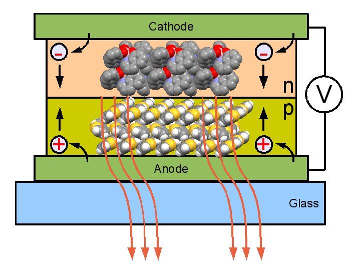
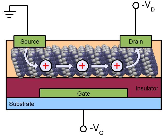
2 Motivation OLED para Sexiphenyl (6P) (C36H26) OFET Pentacene (5A) (C22H14) Slide 2


3 Outline Methods and Materials Cohesive, Surface, and Adsorption Energies Growth of Chain like Molecules on Mica Needle Growth and Orientations Critical Cluster Size Terraced Mounds and Step Edge Barrier Slide 3


4 Ab Initio Methods Any Material Coulomb Force Quantum Mechanics atomic nuclei + electrons Band structure Elastic properties vibrations Magnetic properties Optical properties Slide 4
5 Density Functional Theory in a Nutshell Self consistency Approximations: e.g.: LDA, GGA,... Slide 4

6 Cohesive Energy of Molecular Crystals Slide 5
7 Van der Waals Density Functional Nonlocal Correlation Energy leading to van der Waals interaction Exchange Correlation Energy Dion et al, Phys. Rev. Lett. 92, (2004). Slide 6
.")
8 Cohesive Energy of Molecular Crystals Nabok, Puschnig, Ambrosch Draxl, Phys. Rev. B 77, (2008). Slide 7


 4A (0")

![] Nabok et](/docs-images/92/108962360/images/9-7.jpg "al. Phys.")


9 Surface Energies of Molecular Crystals 4A (100) 4A (0 10) 4A (0 01) 4A (110) γ [m J /m 2 ] Nabok et al. Phys. Rev. B 77, (2008); Ambrosch Draxl et al., New J. Phys. 11, (2009). Slide 8
10 Thiophene / Cu(110) d Thiophene@Cu(110): Sony et al., Phys. Rev. Lett. 99, (2007). PTCDA@Cu,Ag,Au(111): Romaner et al., New. J. Phys. 11, (2009). Slide 9
11 Outline Methods and Materials Cohesive, Surface, and Adsorption Energies Growth of Chain like Molecules on Mica Needle Growth and Orientations Critical Cluster Size Terraced Mounds and Step Edge Barrier Slide 3
12 Nano Needles on Mica Parallel alignment only for phenylenes Anisotropy for thiophenes and co oligomers Macroscopic polarized light emission only for parallel alignment Simbrunner et al., JACS 133, 3056 (2011). Slide 10

13 Mica Substrates Muscovite Phlogopite Slide 11


14 Sexiphenyl / Mica Muscovite Phlogopite AFM Slide 12
15 Growth Models (1) Electric fields of mica align molecules F. Balzer et al., J. Vac. Sci. Technol. B, 26, 1619, (2008). L. Kankate et al., Thin Solid Films 518, 130, (2009). (2) Alignment by geometry/symmetry of mica and molecule Simbrunner et al., JACS 133, 3056 (2011). Methodology Force field simulations Adsorption energy as a function of adsorption position and orientation Substrates: muscovite pyrophyllite phlogopite talc No charges, but the same surface corrugation Slide 13
16 6T vs. 6P on Micas Slide 14

17 6T vs. 6P on Micas Experiment Slide 15
18 6T vs. 6P on Micas Slide 15
19 6T vs. 6P on Micas Slide 15


20 Re Adjustment of Molecular Orientation Slide 16
21 Outline Methods and Materials Cohesive, Surface, and Adsorption Energies Growth of Chain like Molecules on Mica Needle Growth and Orientations Critical Cluster Size Terraced Mounds and Step Edge Barrier Slide 3


22 Island Growth on Amorphous Mica AFM image Amorphous Mica (ion bombarded) 10 x 10 µm² T = 300 K θ = 0.32 ML F = 0.02 ML/min Observation of islands consisting of standing p 6P What is the critical cluster size? Transistion from lying to standing p 6P? Potocar et al., PRB 83, (2011). Slide 17
23 p 6P / p 6P(001) p 6P(001) as model substrate with weak Interactions top view side view Adsorption geometry: Slide 18
 as model")


24 p 6P / p 6P(001) p 6P(001) as model substrate with weak Interactions top view side view Adsorption geometry: Energy landscape Diffusion path: b Slide 18
25 Lying bs. Standing p 6P Ebinding = Encluster / n Elying molecule Slide 19


26 Lying bs. Standing p 6P Critical cluster: Eb = 3 x 0.5 = 1.5 ev Talk N14 4: A. Winkler Ebinding = Encluster / n Elying molecule Slide 19
27 Outline Methods and Materials Cohesive, Surface, and Adsorption Energies Growth of Chain like Molecules on Mica Needle Growth and Orientations Critical Cluster Size Terraced Mounds and Step Edge Barrier Slide 3


28 2.6 nm Terraced Mounds AFM image: Sexiphenyl grown on a disordered mica surface Slide 20
29 Ehrlich Schwoebel Barrier (ESB) Diffusion on a terrace Interlayer jump rate Slide 21
2 AFM image: Film thickness = 30 nm 2nd")
30 Sexiphenyl on Mica Ehrlich Schwoebel Barrier = 0.67 ev = residence time (deposition time)2 AFM image: Film thickness = 30 nm 2nd layer nucleation rate Slide 22


31 Step Edge Barrier Peter Puschnig, EMRS2011, Nice, May 9 th May 13th Slide 23

32 Step Edge Barrier in te rm o lecu la r in te ra ctio n s 1 2 e n e rg y co st fo r b e n d in g Slide 24


33 Layer Dependent ESB ESB 0.26 v s Slide 25
.")
34 Layer Dependent ESB ab in itio DFT E xpe rim e nt S im u la tio n E m p irica l po te ntials G. Hlawacek et al., Science 321, 108 (2008). Slide 26
35 Summary Van der Waals Interactions within DFT Organic / organic works fine; organic / metal interactions still problematic Nabok et al., PRB 77, (2008). Sony et al., PRL. 99, (2007). Romaner et al., NJP 11, (2009). Nano Needle Orientation on Mica Alignment by geometry/symmetry of mica and molecule Simbrunner et al., JACS 133, 3056 (2011). Island Growth on Amorphous Mica Critical cluster = 2 3, Transition lying standing p 6P about 15 molecules Potocar et al., PRB 83, (2011). Step Edge Barriers Some success in understanding certain kinetic barrieres, but still a lot of work to do... G. Hlawacek et al., Science 321, 108 (2008); see also: Goose et al., PRB 81, (2010). Slide 27


36 Collaborations and Funding Lehrstuhl für Atomistic Modelling and Design of Materials, MU Leoben Dmitrii Nabok, Priya Sony, Lorenz Romaner Claudia Ambrosch Draxl Institut für Physik, MU Leoben Quan Shen, Stefan Lorbek, Gregor Hlawacek Christian Teichert Solid State Physics, JKU Linz, Austria Clemens Simbrunner Helmut Sitter Institut für Festkörperphysik, TU Graz, Austria T. Potocar, Paul Frank Adolf Winkler Tatjana Djuric Roland Resel The work is part of the National Research Network Interface controlled and functionalized organic films Slide 28
Growth and Electronic Structure of Organic Molecular Layers Studied by Density Functional Theory
 Growth and Electronic Structure of Organic Molecular Layers Studied by Density Functional Theory Slide 1 Motivation OLED para-sexiphenyl (6P) (C36H26) OFET Pentacene (5A) (C22H14) Slide 2 Outline 1. Density
Theoretical approaches towards the understanding of organic semiconductors:
 Claudia Ambrosch-Draxl Chair of Atomistic Modelling and Design of Materials University of Leoben Theoretical approaches towards the understanding of organic semiconductors: from electronic and optical
Determination of critical island size in -sexiphenyl islands on SiO using capture-zone scaling
 Determination of critical island size in -sexiphenyl islands on SiO using capture-zone scaling S. Lorbek, G. Hlawacek, C. Teichert To cite this version: S. Lorbek, G. Hlawacek, C. Teichert. Determination
Orbital Tomography: A Method to Obtain the Orbital-Projected DOS from ARPES
 Orbital Tomography: A Method to Obtain the Orbital-Projected DOS from ARPES Motivation ARPES data from Stephen Berkebile et al. (2007) hν (21eV) ARPES Intensity e- (20-3) Uniaxially ordered para-sexiphenyl
Initial Stages of Growth of Organic Semiconductors on Graphene
 Initial Stages of Growth of Organic Semiconductors on Graphene Presented by: Manisha Chhikara Supervisor: Prof. Dr. Gvido Bratina University of Nova Gorica Outline Introduction to Graphene Fabrication
Metal/Organic Interfaces
 Metal/Organic Interfaces from first-principles Georg Heimel Institut für f r Physik, Humboldt-Universit Universität t zu Berlin Dresden, 12.02.2009 Outline Investigated Systems / Motivation Methods Overview
X-ray diffraction and Crystal Structure Solutions from Thin Films
 X-ray diffraction and Crystal Structure Solutions from Thin Films Ingo Salzmann Humboldt-Universität zu Berlin Institut für Physik Overview Experimental technique X-ray diffraction The principal phenomenon
Pattern formation by step edge barriers: The growth of spirals and wedding cakes
 Pattern formation by step edge barriers: The growth of spirals and wedding cakes Joachim Krug Institut für Theoretische Physik, Universität zu Köln MRS Fall Meeting, Boston, 11/26/2007 Kinetic growth modes
A Momentum Space View of the Surface Chemical Bond - Supplementary Information
 A Momentum Space View of the Surface Chemical Bond - Supplementary Information Stephen Berkebile, a Thomas Ules, a Peter Puschnig, b Lorenz Romaner, b Georg Koller, a Alexander J. Fleming, a Konstantin
Christian Ratsch, UCLA
 Strain Dependence of Microscopic Parameters and its Effects on Ordering during Epitaxial Growth Christian Ratsch, UCLA Institute for Pure and Applied Mathematics, and Department of Mathematics Collaborators:
Introduction to Density Functional Theory
 Introduction to Density Functional Theory S. Sharma Institut für Physik Karl-Franzens-Universität Graz, Austria 19th October 2005 Synopsis Motivation 1 Motivation : where can one use DFT 2 : 1 Elementary
Organic Nanofibers from PPTPP
 Organic Nanofibers from PPTPP 1 1 2 1 Frank Balzer, Manuela Schiek, Arne Lützeu and Horst-Günter Rubahn 1 Syddansk Universitet, Mads Clausen Institute, NanoSYD, Alsion 2, DK-6400 Sønderborg, Denmark E-mail:
Supplementary Figure 1 Experimental setup for crystal growth. Schematic drawing of the experimental setup for C 8 -BTBT crystal growth.
 Supplementary Figure 1 Experimental setup for crystal growth. Schematic drawing of the experimental setup for C 8 -BTBT crystal growth. Supplementary Figure 2 AFM study of the C 8 -BTBT crystal growth
Outline. Introduction: graphene. Adsorption on graphene: - Chemisorption - Physisorption. Summary
 Outline Introduction: graphene Adsorption on graphene: - Chemisorption - Physisorption Summary 1 Electronic band structure: Electronic properties K Γ M v F = 10 6 ms -1 = c/300 massless Dirac particles!
Energy-Level Alignment at the Interface of Graphene Fluoride and Boron Nitride Monolayers: An Investigation by Many-Body Perturbation Theory
 Supporting Information Energy-Level Alignment at the Interface of Graphene Fluoride and Boron Nitride Monolayers: An Investigation by Many-Body Perturbation Theory Qiang Fu, Dmitrii Nabok, and Claudia
WINTERSCHOOL ON ORGANIC ELECTRONICS Fundamental Properties of Devices Sensors, Transistors and Solar Cells
 WINTERSCHOOL ON ORGANIC ELECTRONICS March 6 th March 12 th, 2010 Universitäts-Sportheim Planneralm Donnersbach, Austria March 6th March 7th March 8th March 9th March 10th March 11th March 12th Saturday
Designing Graphene for Hydrogen Storage
 Designing Graphene for Hydrogen Storage Stefan Heun NEST, Istituto Nanoscienze-CNR and Scuola Normale Superiore Pisa, Italy Outline Introduction to Hydrogen Storage Epitaxial Graphene Hydrogen Storage
Spectroscopies for Unoccupied States = Electrons
 Spectroscopies for Unoccupied States = Electrons Photoemission 1 Hole Inverse Photoemission 1 Electron Tunneling Spectroscopy 1 Electron/Hole Emission 1 Hole Absorption Will be discussed with core levels
Help me understanding the effect of organic acceptor molecules on coinage metals.
 Help me understanding the effect of organic acceptor molecules on coinage metals. Gerold M. Rangger, 1 Oliver T. Hofmann, 1 Anna M. Track, 1 Ferdinand Rissner, 1 Lorenz Romaner, 1,2 Georg Heimel, 2 Benjamin
Hydrogenated Graphene
 Hydrogenated Graphene Stefan Heun NEST, Istituto Nanoscienze-CNR and Scuola Normale Superiore Pisa, Italy Outline Epitaxial Graphene Hydrogen Chemisorbed on Graphene Hydrogen-Intercalated Graphene Outline
Flux heterogeneity through incidence angle and particle energy in steering-enhanced growth
 Flux heterogeneity through incidence angle and particle energy in steering-enhanced growth Herbert Wormeester* and Bene Poelsema MESA Research Institute, University of Twente, P.O. Box 217, 7500 AE Enschede,
Surface Physics Surface Diffusion. Assistant: Dr. Enrico Gnecco NCCR Nanoscale Science
 Surface Physics 008 8. Surface Diffusion Assistant: Dr. Enrico Gnecco NCCR Nanoscale Science Random-Walk Motion Thermal motion of an adatom on an ideal crystal surface: - Thermal excitation the adatom
Optimized Effective Potential method for non-collinear Spin-DFT: view to spin-dynamics
 Optimized Effective Potential method for non-collinear Spin-DFT: view to spin-dynamics Sangeeta Sharma 1,2, J. K. Dewhurst 3, C. Ambrosch-Draxl 4, S. Pittalis 2, S. Kurth 2, N. Helbig 2, S. Shallcross
Teoría del Funcional de la Densidad (Density Functional Theory)
") Teoría del Funcional de la Densidad (Density Functional Theory) Motivation: limitations of the standard approach based on the wave function. The electronic density n(r) as the key variable: Functionals
Teoría del Funcional de la Densidad (Density Functional Theory) Motivation: limitations of the standard approach based on the wave function. The electronic density n(r) as the key variable: Functionals
Spin-orbit coupling fields in Fe/GaAs heterostructures
 Spin-orbit coupling fields in Fe/GaAs heterostructures Outline motivation a simplified model of the Fe/GaAs heterostructure extracting spin-orbit coupling parameters spin-orbit coupling field conclusions
III-V nanostructured materials synthesized by MBE droplet epitaxy
 III-V nanostructured materials synthesized by MBE droplet epitaxy E.A. Anyebe 1, C. C. Yu 1, Q. Zhuang 1,*, B. Robinson 1, O Kolosov 1, V. Fal ko 1, R. Young 1, M Hayne 1, A. Sanchez 2, D. Hynes 2, and
Accuracy of adiabatic DFT calculations in the description of molecular dissociation at metal surfaces
 Accuracy of adiabatic DFT calculations in the description of molecular dissociation at metal surfaces Ricardo Díez Muiño Centro de Física de Materiales, Centro Mixto CSIC-UPV/EHU San Sebastián (Spain)
Molecular Dynamics on the Angstrom Scale
 Probing Interface Reactions by STM: Molecular Dynamics on the Angstrom Scale Zhisheng Li Prof. Richard Osgood Laboratory for Light-Surface Interactions, Columbia University Outline Motivation: Why do we
Kinetics and Functionality of Cu-coordinated Pyridyl-porphyrin Supramolecular Self-assembly on a Au(111) Surface
 Surface") Kinetics and Functionality of Cu-coordinated Pyridyl-porphyrin Supramolecular Self-assembly on a Au(111) Surface LI, Yang, MPhil candidate, Physics, HKUST Supervisor, Prof. LIN, Nian 2012-08-08 Outline
Kinetics and Functionality of Cu-coordinated Pyridyl-porphyrin Supramolecular Self-assembly on a Au(111) Surface LI, Yang, MPhil candidate, Physics, HKUST Supervisor, Prof. LIN, Nian 2012-08-08 Outline
Optical Spectroscopies of Thin Films and Interfaces. Dietrich R. T. Zahn Institut für Physik, Technische Universität Chemnitz, Germany
 Optical Spectroscopies of Thin Films and Interfaces Dietrich R. T. Zahn Institut für Physik, Technische Universität Chemnitz, Germany 1. Introduction 2. Vibrational Spectroscopies (Raman and Infrared)
Stress Evolution during Film Growth: CTC! Stress Evolution during Film Growth: CTC!
 When Vapor Deforms Metal: Thermodynamics of Deposition Flux Dependent Intrinsic Film Stress M.J. Rost Kamerlingh Onnes Laboratory, Leiden University (NL) Rost@physics.leidenuniv.nl www.physics.leidenuniv.nl/rost
Kinetic Monte Carlo: from transition probabilities to transition rates
 Kinetic Monte Carlo: from transition probabilities to transition rates With MD we can only reproduce the dynamics of the system for 100 ns. Slow thermallyactivated processes, such as diffusion, cannot
Lecture 30: Kinetics of Epitaxial Growth: Surface Diffusion and
 Lecture 30: Kinetics of Epitaxial Growth: Surface Diffusion and Nucleation Today s topics Understanding the basics of epitaxial techniques used for surface growth of crystalline structures (films, or layers).
Substrate-mediated band-dispersion of adsorbate molecular states - Supplementary Information
 Substrate-mediated band-dispersion of adsorbate molecular states - Supplementary Information M. Wießner, 1, 2 J. Ziroff, 1, 2 F. Forster, 1, 2 M. Arita, 3 K. Shimada, 3 P. Puschnig, 4 A. Schöll*, 1, 2,
Growth morphology evolution in real time and real space
 Growth morphology evolution in real time and real space Joachim Krug Institut für Theoretische Physik, Universität zu Köln Multilayer growth modes and interlayer transport The Ehrlich-Schwoebel effect
Crystalline Surfaces for Laser Metrology
 Crystalline Surfaces for Laser Metrology A.V. Latyshev, Institute of Semiconductor Physics SB RAS, Novosibirsk, Russia Abstract: The number of methodological recommendations has been pronounced to describe
Lecture 10 Thin Film Growth
 Lecture 10 Thin Film Growth 1/76 Announcements Homework: Homework Number 2 is returned today, please pick it up from me at the end of the class. Solutions are online. Homework 3 will be set Thursday (2
Multi-Scale Modeling from First Principles
 m mm Multi-Scale Modeling from First Principles μm nm m mm μm nm space space Predictive modeling and simulations must address all time and Continuum Equations, densityfunctional space scales Rate Equations
Molecular and Biological Matter Nano-Science in Motion
 Molecular and Biological Matter Nano-Science in Motion F D n+1 n n-1 1 Frank Schreiber http://www.soft-matter.uni-tuebingen.de Molecular and Biological Matter Nano-Science in Motion Welche Themen gibt
Temperature-dependence of magnetism of free Fe clusters
 Temperature-dependence of magnetism of free Fe clusters O. Šipr 1, S. Bornemann 2, J. Minár 2, S. Polesya 2, H. Ebert 2 1 Institute of Physics, Academy of Sciences CR, Prague, Czech Republic 2 Universität
x-ray reflectivity: structural characterisation of thin films for organic electronics
 x-ray reflectivity: structural characterisation of thin films for organic electronics Roland Resel, Oliver Werzer, Institute of Solid State Physics, Graz University of Technology 1 DHS900 content x-ray
Understanding the growth mechanism of graphene on Ge/Si(001) surfaces
 surfaces") Supplementary material for the manuscript: Understanding the growth mechanism of graphene on Ge/Si(001) surfaces J. Dabrowski, 1 G. Lippert, 1 J. Avila, 2 J. Baringhaus, 3 I. Colambo, 4 Yu. S. Dedkov,
Supplementary material for the manuscript: Understanding the growth mechanism of graphene on Ge/Si(001) surfaces J. Dabrowski, 1 G. Lippert, 1 J. Avila, 2 J. Baringhaus, 3 I. Colambo, 4 Yu. S. Dedkov,
First-Principles Modeling of Charge Transport in Molecular Junctions
 First-Principles Modeling of Charge Transport in Molecular Junctions Chao-Cheng Kaun Research Center for Applied Sciences, Academia Sinica Department of Physics, National Tsing Hua University September
DENSITY FUNCTIONAL THEORY FOR NON-THEORISTS JOHN P. PERDEW DEPARTMENTS OF PHYSICS AND CHEMISTRY TEMPLE UNIVERSITY
 DENSITY FUNCTIONAL THEORY FOR NON-THEORISTS JOHN P. PERDEW DEPARTMENTS OF PHYSICS AND CHEMISTRY TEMPLE UNIVERSITY A TUTORIAL FOR PHYSICAL SCIENTISTS WHO MAY OR MAY NOT HATE EQUATIONS AND PROOFS REFERENCES
Adsorption, desorption, and diffusion on surfaces. Joachim Schnadt Divsion of Synchrotron Radiation Research Department of Physics
 Adsorption, desorption, and diffusion on surfaces Joachim Schnadt Divsion of Synchrotron Radiation Research Department of Physics Adsorption and desorption Adsorption Desorption Chemisorption: formation
tunneling theory of few interacting atoms in a trap
 tunneling theory of few interacting atoms in a trap Massimo Rontani CNR-NANO Research Center S3, Modena, Italy www.nano.cnr.it Pino D Amico, Andrea Secchi, Elisa Molinari G. Maruccio, M. Janson, C. Meyer,
Optimized Effective Potential method for non-collinear Spin-DFT: view to spindynamics
 Optimized Effective Potential method for non-collinear Spin-DFT: view to spindynamics S. Sharma and E. K. U. Gross nstitut für Theoretische Physik, FU Berlin Fritz-Haber nstitut, Berlin 21 Sept 2006 Synopsis
Electron transport through molecular junctions and FHI-aims
 STM m metallic surface Electron transport through molecular junctions and FHI-aims Alexei Bagrets Inst. of Nanotechnology (INT) & Steinbuch Centre for Computing (SCC) @ Karlsruhe Institute of Technology
Physics and Material Science of Semiconductor Nanostructures
 Physics and Material Science of Semiconductor Nanostructures PHYS 570P Prof. Oana Malis Email: omalis@purdue.edu Course website: http://www.physics.purdue.edu/academic_programs/courses/phys570p/ Lecture
Design of Efficient Catalysts with Double Transition Metal. Atoms on C 2 N Layer
 Supporting Information Design of Efficient Catalysts with Double Transition Metal Atoms on C 2 N Layer Xiyu Li, 1, Wenhui Zhong, 2, Peng Cui, 1 Jun Li, 1 Jun Jiang 1, * 1 Hefei National Laboratory for
Curvature-enhanced Spin-orbit Coupling and Spinterface Effect in Fullerene-based Spin Valves
 Supplementary Information Curvature-enhanced Spin-orbit Coupling and Spinterface Effect in Fullerene-based Spin Valves Shiheng Liang 1, Rugang Geng 1, Baishun Yang 2, Wenbo Zhao 3, Ram Chandra Subedi 1,
Widely Tunable and Intense Mid-Infrared PL Emission from Epitaxial Pb(Sr)Te Quantum Dots in a CdTe Matrix
Te Quantum Dots in a CdTe Matrix") Widely Tunable and Intense Mid-Infrared PL Emission from Epitaxial Pb(Sr)Te Quantum Dots in a Matrix S. Kriechbaumer 1, T. Schwarzl 1, H. Groiss 1, W. Heiss 1, F. Schäffler 1,T. Wojtowicz 2, K. Koike 3,
Widely Tunable and Intense Mid-Infrared PL Emission from Epitaxial Pb(Sr)Te Quantum Dots in a Matrix S. Kriechbaumer 1, T. Schwarzl 1, H. Groiss 1, W. Heiss 1, F. Schäffler 1,T. Wojtowicz 2, K. Koike 3,
Supplementary Information:
 Supplementary Figures Supplementary Information: a b 1 2 3 0 ΔZ (pm) 66 Supplementary Figure 1. Xe adsorbed on a Cu(111) surface. (a) Scanning tunnelling microscopy (STM) topography of Xe layer adsorbed
Institut des NanoSciences de Paris
 CNRS / Photothèque Cyril Frésillon Institut des NanoSciences de Paris Polarity in low dimensions: MgO nano-ribbons on Au(111) J. Goniakowski, C. Noguera Institut des Nanosciences de Paris, CNRS & Université
J 12 J 23 J 34. Driving forces in the nano-magnetism world. Intra-atomic exchange, electron correlation effects: Inter-atomic exchange: MAGNETIC ORDER
 Driving forces in the nano-magnetism world Intra-atomic exchange, electron correlation effects: LOCAL (ATOMIC) MAGNETIC MOMENTS m d or f electrons Inter-atomic exchange: MAGNETIC ORDER H exc J S S i j
Semiconductor Polymer
 Semiconductor Polymer Organic Semiconductor for Flexible Electronics Introduction: An organic semiconductor is an organic compound that possesses similar properties to inorganic semiconductors with hole
Structural and Mechanical Properties of Nanostructures
 Master s in nanoscience Nanostructural properties Mechanical properties Structural and Mechanical Properties of Nanostructures Prof. Angel Rubio Dr. Letizia Chiodo Dpto. Fisica de Materiales, Facultad
SUPPLEMENTARY INFORMATION
 SUPPLEMENTARY INFORMATION Towards wafer-size graphene layers by atmospheric pressure graphitization of silicon carbide Supporting online material Konstantin V. Emtsev 1, Aaron Bostwick 2, Karsten Horn
Impurities and graphene hybrid structures: insights from first-principles theory
 Impurities and graphene hybrid structures: insights from first-principles theory Tim Wehling Institute for Theoretical Physics and Bremen Center for Computational Materials Science University of Bremen
Physics in two dimensions in the lab
 Physics in two dimensions in the lab Nanodevice Physics Lab David Cobden PAB 308 Collaborators at UW Oscar Vilches (Low Temperature Lab) Xiaodong Xu (Nanoscale Optoelectronics Lab) Jiun Haw Chu (Quantum
Surface Composition Mapping Of Semiconductor Quantum Dots. Stefan Heun, Laboratorio TASC INFM-CNR, Trieste, Italy.
 Surface Composition Mapping Of Semiconductor Quantum Dots Stefan Heun, Laboratorio TASC INFM-CNR, Trieste, Italy. Motivation Quantum Dot Applications based on their particular electronic properties (confinement)
Zero- or two-dimensional?
 Stacked layers of submonolayer InAs in GaAs: Zero- or two-dimensional? S. Harrison*, M. Young, M. Hayne, P. D. Hodgson, R. J. Young A. Schliwa, A. Strittmatter, A. Lenz, H. Eisele, U. W. Pohl, D. Bimberg
Effects of substrate rotation in oblique-incidence metal(100) epitaxial growth
 epitaxial growth") W Recently, using a simplified ballistic deposition model 6 which includes the effects of downward funneling (DF) 8 and rapid diffusion on () facets, two of us have shown that many of the qualitative and
W Recently, using a simplified ballistic deposition model 6 which includes the effects of downward funneling (DF) 8 and rapid diffusion on () facets, two of us have shown that many of the qualitative and
arxiv: v1 [cond-mat.stat-mech] 23 Aug 2011
![arxiv: v1 [cond-mat.stat-mech] 23 Aug 2011](/thumbs/93/113375882.jpg "arxiv: v1 [cond-mat.stat-mech] 23 Aug 2011") arxiv:1108.4655v1 [cond-mat.stat-mech] 23 Aug 2011 Kinetic modelling of epitaxial film growth with upand downward step barriers F.F. Leal 1,2, T. J. Oliveira 1 and S. C. Ferreira 1 1 Departamento de Física
arxiv:1108.4655v1 [cond-mat.stat-mech] 23 Aug 2011 Kinetic modelling of epitaxial film growth with upand downward step barriers F.F. Leal 1,2, T. J. Oliveira 1 and S. C. Ferreira 1 1 Departamento de Física
Optimizing Graphene Morphology on SiC(0001)
") Optimizing Graphene Morphology on SiC(0001) James B. Hannon Rudolf M. Tromp Graphene sheets Graphene sheets can be formed into 0D,1D, 2D, and 3D structures Chemically inert Intrinsically high carrier mobility
Optimizing Graphene Morphology on SiC(0001) James B. Hannon Rudolf M. Tromp Graphene sheets Graphene sheets can be formed into 0D,1D, 2D, and 3D structures Chemically inert Intrinsically high carrier mobility
Topological insulator gap in graphene with heavy adatoms
 Topological insulator gap in graphene with heavy adatoms ES2013, College of William and Mary Ruqian Wu Department of Physics and Astronomy, University of California, Irvine, California 92697 Supported
Intermolecular Forces in Density Functional Theory
 Intermolecular Forces in Density Functional Theory Problems of DFT Peter Pulay at WATOC2005: There are 3 problems with DFT 1. Accuracy does not converge 2. Spin states of open shell systems often incorrect
X-ray Imaging and Spectroscopy of Individual Nanoparticles
 X-ray Imaging and Spectroscopy of Individual Nanoparticles A. Fraile Rodríguez, F. Nolting Swiss Light Source Paul Scherrer Institut, Switzerland Intensity [a.u.] 1.4 1.3 1.2 1.1 D 8 nm 1 1 2 3 1.0 770
New applications of Diffusion Quantum Monte Carlo
 New applications of Diffusion Quantum Monte Carlo Paul R. C. Kent (ORNL) Graphite: P. Ganesh, J. Kim, C. Park, M. Yoon, F. A. Reboredo (ORNL) Platinum: W. Parker, A. Benali, N. Romero (ANL), J. Greeley
Supplementary Figure 1(a) The trajectory of the levitated pyrolytic graphite test sample (blue curve) and
 The trajectory of the levitated pyrolytic graphite test sample (blue curve) and") Supplementary Figure 1(a) The trajectory of the levitated pyrolytic graphite test sample (blue curve) and the envelope from free vibration theory (red curve). (b) The FFT of the displacement-time curve
Supplementary Figure 1(a) The trajectory of the levitated pyrolytic graphite test sample (blue curve) and the envelope from free vibration theory (red curve). (b) The FFT of the displacement-time curve
Optical SHG and RAS of molecular adsorption at Si(001) step edges
 step edges") Optical SHG and RAS of molecular adsorption at Si(001) step edges Robert Ehlert, Jinhee Kwon and Michael C. Downer Department of Physics, The University of Texas at Austin, Austin TX 78712, USA. OSI VI:
Optical SHG and RAS of molecular adsorption at Si(001) step edges Robert Ehlert, Jinhee Kwon and Michael C. Downer Department of Physics, The University of Texas at Austin, Austin TX 78712, USA. OSI VI:
From manipulation of the charge state to imaging of individual molecular orbitals and bond formation
 Scanning Probe Microscopy of Adsorbates on Insulating Films: From manipulation of the charge state to imaging of individual molecular orbitals and bond formation Gerhard Meyer, Jascha Repp, Peter Liljeroth
Nanoelectronics. Topics
 Nanoelectronics Topics Moore s Law Inorganic nanoelectronic devices Resonant tunneling Quantum dots Single electron transistors Motivation for molecular electronics The review article Overview of Nanoelectronic
for investigating Lars Heinke Fritz-Haber-Institute of the Max-Planck-Society, Berlin Jörg Kärger University Leipzig
 Using kinetic Monte Carlo simulations for investigating surface barriers in nanoporous materials Lars Heinke Fritz-Haber-Institute of the Max-Planck-Society, Berlin Jörg Kärger University Leipzig Com-Phys-09
Triplet state diffusion in organometallic and organic semiconductors
 Triplet state diffusion in organometallic and organic semiconductors Prof. Anna Köhler Experimental Physik II University of Bayreuth Germany From materials properties To device applications Organic semiconductors
Monte Carlo simulation of Secondary Electron Yield for Noble metals Martina Azzolini, Nicola M. Pugno, Simone Taioli, Maurizio Dapor
 Monte Carlo simulation of Secondary Electron Yield for Noble metals Martina Azzolini, Nicola M. Pugno, Simone Taioli, Maurizio Dapor ECLOUD 18 - Elba Island- 3-7 June 2018 OUTLINE Description of the Monte
Reactive Force Field & Molecular Dynamics Simulations (Theory & Applications)
") Reactive Force Field & Molecular Dynamics Simulations (Theory & Applications) Ying Li Collaboratory for Advanced Computing & Simulations Department of Chemical Engineering & Materials Science Department
Reactive Force Field & Molecular Dynamics Simulations (Theory & Applications) Ying Li Collaboratory for Advanced Computing & Simulations Department of Chemical Engineering & Materials Science Department
Physics of Semiconductors
 Physics of Semiconductors 9 th 2016.6.13 Shingo Katsumoto Department of Physics and Institute for Solid State Physics University of Tokyo Site for uploading answer sheet Outline today Answer to the question
Sensitization mechanisms of chemically amplified EUV resists and resist design for 22 nm node. Takahiro Kozawa and Seiichi Tagawa
 Sensitization mechanisms of chemically amplified EUV resists and resist design for 22 nm node Takahiro Kozawa and Seiichi Tagawa The Institute of Scientific and Industrial Research, Osaka University, 8-1
Contents. Preface XI Symbols and Abbreviations XIII. 1 Introduction 1
 V Contents Preface XI Symbols and Abbreviations XIII 1 Introduction 1 2 Van der Waals Forces 5 2.1 Van der Waals Forces Between Molecules 5 2.1.1 Coulomb Interaction 5 2.1.2 Monopole Dipole Interaction
Spin-orbit proximity effects in graphene on TMDCs. Jaroslav Fabian
 Hvar, 4.10.2017 Spin-orbit proximity effects in graphene on TMDCs Jaroslav Fabian Institute for Theoretical Physics University of Regensburg SFB1277 GRK TI SPP 1666 SFB689 GRK1570 SPP 1538 Arbeitsgruppe
Carbon nanotubes in a nutshell. Graphite band structure. What is a carbon nanotube? Start by considering graphite.
 Carbon nanotubes in a nutshell What is a carbon nanotube? Start by considering graphite. sp 2 bonded carbon. Each atom connected to 3 neighbors w/ 120 degree bond angles. Hybridized π bonding across whole
Non-collinear OEP for solids: SDFT vs CSDFT
 Non-collinear OEP for solids: SDFT vs Sangeeta Sharma 1,2, J. K. Dewhurst 3 S. Pittalis 2, S. Kurth 2, S. Shallcross 4 and E. K. U. Gross 2 1. Fritz-Haber nstitut of the Max Planck Society, Berlin, Germany
The Electronic Structure of Dye- Sensitized TiO 2 Clusters from Many- Body Perturbation Theory
 The Electronic Structure of Dye- Sensitized TiO 2 Clusters from Many- Body Perturbation Theory Noa Marom Center for Computational Materials Institute for Computational Engineering and Sciences The University
Modeling the sputter deposition of thin film photovoltaics using long time scale dynamics techniques
 Loughborough University Institutional Repository Modeling the sputter deposition of thin film photovoltaics using long time scale dynamics techniques This item was submitted to Loughborough University's
All electron optimized effective potential method for solids
 All electron optimized effective potential method for solids Institut für Theoretische Physik Freie Universität Berlin, Germany and Fritz Haber Institute of the Max Planck Society, Berlin, Germany. 22
Binding energy of 2D materials using Quantum Monte Carlo
 Quantum Monte Carlo in the Apuan Alps IX International Workshop, 26th July to 2nd August 2014 The Apuan Alps Centre for Physics @ TTI, Vallico Sotto, Tuscany, Italy Binding energy of 2D materials using
1. Introduction to Clusters
 1. Introduction to Clusters 1.1 The Field of Clusters Atomic clusters are aggregates of atoms containing from few to a few thousand atoms. Due to their small size, the properties of the clusters are, in
Computer Simulations and Nanotechnology
 Computer Simulations and Nanotechnology Intro: - Making use of high speed modern computers, and therefore nanotechnology - Contributing to the development of nanotechnology Tools: A. Starting from basic
Magnetic interaction at the metalorganic molecule substrate interface: Insights from first-principles calculations
 Magnetic interaction at the metalorganic molecule substrate interface: Insights from first-principles calculations Peter M. Oppeneer with Kartick Tarafder and Ehesan Ali Department of Physics and Astronomy,
Experiment Section Fig. S1 Fig. S2
 Electronic Supplementary Material (ESI) for ChemComm. This journal is The Royal Society of Chemistry 2018 Supplementary Materials Experiment Section The STM experiments were carried out in an ultrahigh
Challenges in understanding defects in organic materials: a theorist view, focus on conjugated polymers
 Challenges in understanding defects in organic materials: a theorist view, focus on conjugated polymers Marília J. Caldas University of São Paulo Scientia Vinces 1 Ronaldo Giro Melissa F. Siqueira-Pinto
Self-Assembly of Two-Dimensional Organic Networks Containing Heavy Metals (Pb, Bi) and Preparation of Spin-Polarized Scanning Tunneling Microscope
 and Preparation of Spin-Polarized Scanning Tunneling Microscope") MPhil Thesis Defense Self-Assembly of Two-Dimensional Organic Networks Containing Heavy Metals (Pb, Bi) and Preparation of Spin-Polarized Scanning Tunneling Microscope Presented by CHEN Cheng 12 th Aug.
MPhil Thesis Defense Self-Assembly of Two-Dimensional Organic Networks Containing Heavy Metals (Pb, Bi) and Preparation of Spin-Polarized Scanning Tunneling Microscope Presented by CHEN Cheng 12 th Aug.
Step-induced electronic resonance at vicinal Si(001) observed by spectroscopic SHG and RAS
 observed by spectroscopic SHG and RAS") Step-induced electronic resonance at vicinal Si(001) observed by spectroscopic SHG and RAS Robert Ehlert, Jinhee Kwon and Michael C. Downer Department of Physics, The University of Texas at Austin, Austin
Step-induced electronic resonance at vicinal Si(001) observed by spectroscopic SHG and RAS Robert Ehlert, Jinhee Kwon and Michael C. Downer Department of Physics, The University of Texas at Austin, Austin
Carbon nanotubes in a nutshell
 Carbon nanotubes in a nutshell What is a carbon nanotube? Start by considering graphite. sp 2 bonded carbon. Each atom connected to 3 neighbors w/ 120 degree bond angles. Hybridized π bonding across whole
Non-adiabatic Electron-ion Dynamics in Ion-irradiated 2D Materials
 Non-adiabatic Electron-ion Dynamics in Ion-irradiated 2D Materials Alina Kononov, André Schleife University of Illinois at Urbana-Champaign OCI-0725070 ACI-1238993 DE-AC02-06CH11357 Focused Beam Techniques
Structure analysis: Electron diffraction LEED TEM RHEED
 Structure analysis: Electron diffraction LEED: Low Energy Electron Diffraction SPA-LEED: Spot Profile Analysis Low Energy Electron diffraction RHEED: Reflection High Energy Electron Diffraction TEM: Transmission
Polar oxide surfaces and ultra-thin films
 Polar oxide surfaces and ultra-thin films Claudine Noguera Institut des Nanosciences de Paris, CNRS UMR 7588, Université Pierre et Marie Curie (Paris VI) Campus de Boucicaut, 140 rue Lourmel, 75015 Paris
Electronic structure and properties of a few-layer black phosphorus Mikhail Katsnelson
 Electronic structure and properties of a few-layer black phosphorus Mikhail Katsnelson Main collaborators: Sasha Rudenko Shengjun Yuan Rafa Roldan Milton Pereira Sergey Brener Motivation Plenty of 2D materials
Atomistic aspects: the role of DFT calculations
 Atomistic aspects: the role of DFT calculations Peter Kratzer Fritz-Haber-Institut der MPG, Berlin, Germany How to obtain information about the energetics at the atomic level From statistical physics to