(12) United States Patent (10) Patent No.: US 8,853,818 B2
|
|
|
- Natalie Griffith
- 5 years ago
- Views:
Transcription
1 USOO B2 (12) United States Patent (10) Patent No.: US 8,853,818 B2 Lue (45) Date of Patent: Oct. 7, 2014 (54) 3D NAND FLASH MEMORY OTHER PUBLICATIONS (71) Applicant: Hang-Ting Lue, Zhubei (TW) Jung et al., Three Dimensionally Stacked NAND Flash Memory Technology Using Stacking Single Crystal Si Layers on ILD and (72) Inventor: Hang-Ting Lue, Zhubei (TW) Nes Structure for Beyond 30nm Node. IEEE IEDM 2006, Dec. - 15, 4 pages. Johnson et al., 512-Mb PROMWith a Three-Dimensional Array of (73) Assignee: Macronix International Co., Ltd., Diode? Antifuse Memory Cells. IEEE Journal of Solid-State Cir Hsinchu (TW) cuits, vol. 38, No. 11, Nov. 2003, pp Lai et al., A Multi-Layer Stackable Thin-Film Transistor (TFT) (*) Notice: Subject to any disclaimer, the term of this NAND-Type Flash Memory. Electron Devices Meeting, 2006, IEDM '06 International, Dec , 2006, pp patent 1s st adjusted under 35 Tanaka et al., Bit Cost Scalable Technology with Punch and Plug U.S.C. 154(b) by 0 days. Process for Ultra High Density Flash Memory. VLSI Technology, (21) Appl. No.: 13/772, IEEE Symposium on Jun , 2007, pp ppl. No.: 9 * cited by examiner (22) Filed: Feb. 20, 2013 Primary Examiner Calvin Lee (65) Prior Publication Data (74) Attorney, Agent, or Firm Yiding Wu; Haynes Beffel US 2014/ A1 Aug. 21, 2014 & Wolfeld LLP (51) Int. Cl (57) ABSTRACT HOIL 23/52 ( ) A memory device includes an array of NAND strings of HOIL 21/82 ( ) memory cells. The device includes a plurality of stacks of conductive strips separated by insulating material, including (52) S.C. 257/.530: 438/13.1 at least a bottom plane of conductive strips, a plurality of intermediate planes of conductive strips, and a top plane of (58) Field of Classification Search conductive strips. The device includes charge storage struc USPC /216, 266, 131, 467: 365/63, tures in interface regions at cross-points between side Sur 365/185.18; 257/ , faces of the conductive strips in the plurality of intermediate 257 FE21.21 E planes in the stacks and inter-stack semiconductor body ele See application file for complete search history. ments of a plurality of bit line structures. At least one refer ence line structure is arranged orthogonally over the stacks, (56) References Cited including vertical conductive elements between the stacks in U.S. PATENT DOCUMENTS 8,163,616 B2 * 4/2012 Kang et al ,258 8,208,279 B2 * 6/2012 Lue /63 8,363,476 B2 1/2013 Lue et al. 2009, O A1 7/2009 Jin et al. 2012/01828O8 A1 7, 2012 Lue et al. electrical communication with a reference conductor between the bottom plane of conductive strips and a substrate, and linking elements over the stacks connecting the vertical conductive elements. The vertical conductive elements have a higher conductivity than the semiconductor body elements. 17 Claims, 33 Drawing Sheets s 8 :
2 U.S. Patent Oct. 7, 2014 Sheet 1 of 33 US 8,853,818 B O 1 2ZZZZZZZZZZZZZZZZZZZZZZZZZ?? ÈN? FIG. 1
3
4 U.S. Patent Oct. 7, 2014 Sheet 3 of 33 US 8,853,818 B2 NNNNNNNNNNNNNNNNNNNNNNNNN?g? 2 N+ Referen FIG. 3
5
6
7
8 U.S. Patent US 8,853,818 B2 FIG. 7
9 U.S. Patent Oct. 7, 2014 Sheet 8 of 33 US 8,853,818 B2 :: %
10 U.S. Patent Oct. 7, 2014 Sheet 9 Of 33 US 8,853,818 B2 OTHER CIRCUITRY 969 STATE MACHINE DATA IN DATAOU ADDRESS 965 DOUBLE GATE VERTICAL CHANNEL MEMORY ARRAY BASING ARRANGEMENT SUPPLY VOLTAGES
11 U.S. Patent Oct. 7, 2014 Sheet 10 of 33 US 8,853,818 B2 Form assist gate Conductors, and assistgate dielectric On a Substrate Form layers of a first conductive material Separated by insulating material Etch layers of first conductive material to define stacks of conductive strips, including WL and GSL linking elements Form a memory layer on sides of conductive Strips Form a layer of a second conductive material over the memory layer Etch the layer of second conductive material to define bit line structures, a reference line Structure, and a reference Conductor Implant N+ doping material on bit line structures and reference line structure Form decoding structures including interlayer Connectors coupled to WL and GSL linking elements Form overlying conductive layers connected to bit line and reference line structure FIG
12 U.S. Patent Oct. 7, 2014 Sheet 11 of 33 US 8,853,818 B XXXX S& FIG. 11
13 U.S. Patent Oct. 7, 2014 Sheet 12 of 33 US 8,853,818 B2 No.ae"] XX XXXX XXXX S&S --TXUASI-E-A-T-I---- XX &&!!!!!!! & x K & K & g & K g g g g g g g g g g g g : s is x s x x s X s Y s : y : X s. x X x X 1212 FIG. 12
14
15 U.S. Patent US 8,853,818 B2?Â Ø FIG. 14 ~ Ø? Ø ~ ZZZZZZZZZZZZZZZZZZZZZZZOS
16 U.S. Patent Oct. 7, 2014 Sheet 15 Of 33 US 8,853,818 B FIG. 15
17 U.S. Patent Oct. 7, 2014 Sheet 16 of 33 US 8,853,818 B FIG 16
18 U.S. Patent US 8,853,818 B NNNNN FIG. 17
19
20 U.S. Patent Oct. 7, 2014 Sheet 19 Of 33 US 8,853,818 B2 ar FIG. 19
21 U.S. Patent Oct. 7, 2014 Sheet 20 of 33 US 8,853,818 B : : aw 1 9 C O O C 898 : C KO C C C KO C
22 U.S. Patent Oct. 7, 2014 Sheet 21 of 33 US 8,853,818 B2 CXXXXX &S S&S X x XXXXX & KXXXXXX &S XXXXXXXX FIG. 21
23 U.S. Patent Oct. 7, 2014 Sheet 22 of 33 US 8,853,818 B ) -- ( 2240 KO i 3 AV A /Y YV MY AV 1 9 O 5 s XXXX S& XXXX S& XXXX KXXX CXXX
24 U.S. Patent Oct. 7, 2014 Sheet 23 of 33 US 8,853,818 B2 r 2390 : :::::RS ::::XXXX's
25 U.S. Patent US 8,853,818 B FIG. 24
26 U.S. Patent Oct. 7, 2014 Sheet 25 Of 33 US 8,853,818 B2 FIG. 25
27
28
29 U.S. Patent Oct. 7, 2014 Sheet 28 of 33 US 8,853,818 B E
30 U.S. Patent Oct. 7, 2014 Sheet 29 Of 33 US 8,853,818 B2
31
32
33
34

35 1. 3D NAND FLASH MEMORY BACKGROUND OF THE INVENTION 1. Field of the Invention The present invention relates to high density memory devices, and particularly to memory devices in which mul tiple planes of memory cells are arranged to provide a three dimensional 3D array. 2. Description of Related Art As critical dimensions of devices in integrated circuits shrink to the limits of common memory cell technologies, designers have been looking to techniques for stacking mul tiple planes of memory cells to achieve greater storage capac ity, and to achieve lower costs per bit. For example, thin film transistor techniques are applied to charge trapping memory technologies in Lai, et al., A Multi-Layer Stackable Thin Film Transistor (TFT) NAND-Type Flash Memory. IEEE Int l Electron Devices Meeting, Dec. 2006; and in Jung et al., Three Dimensionally Stacked NAND Flash Memory Technology Using Stacking Single Crystal Si Layers on ILD and TANOS Structure for Beyond 30 nm Node. IEEE Int l Electron Devices Meeting, Dec Also, cross-point array techniques have been applied for anti-fuse memory in Johnson et al., 512-Mb PROM. With a Three-Dimensional Array of Diode/Anti-fuse Memory Cells. IEEE J. of Solid-State Circuits, vol. 38, no. 11, November In the design described in Johnson et al., multiple layers of word lines and bit lines are provided, with memory elements at the cross-points. The memory elements comprise a p- polysilicon anode connected to a word line, and an n-polysilicon cathode connected to a bit line, with the anode and cathode separated by anti-fuse material. In the processes described in Lai, et al., Jung, et al. and Johnson, et al., there are several critical lithography steps for each memory layer. Thus, the number of critical lithography steps needed to manufacture the device is multiplied by the number of layers that are implemented. So, although the benefits of higher density are achieved using three-dimen sional (3D) arrays, the higher manufacturing costs limit the use of the technology. Another structure that provides vertical NAND cells in a charge trapping memory technology is described in Tanaka et al., Bit Cost Scalable Technology with Punch and Plug Pro cess for Ultra High Density Flash Memory Sympo sium on VLSI Technology Digest of Technical Papers, Jun. 2007, pages The structure described in Tanaka et al. includes a multi-gate field effect transistor structure hav ing a vertical channel which operates like a NAND gate, using silicon-oxide-nitride-oxide-silicon SONOS charge trapping technology to create a storage site at each gate?vertical chan nel interface. The memory structure is based on a pillar of semiconductor material arranged as the vertical channel for the multi-gate cell, with a lower select gate adjacent the Substrate, and an upper select gate on top. A plurality of horizontal control gates is formed using planar electrode lay ers that intersect with the pillars. The planar electrode layers used for the control gates do not require critical lithography, and thereby save costs. However, many critical lithography steps are required for each of the vertical cells. Also, there is a limit in the number of control gates that can be layered in this way, determined by such factors as the conductivity of the Vertical channel, program and erase processes that are used and so on. It is desirable to provide a structure for three-dimensional integrated circuit memory with a low manufacturing cost, including reliable, very Small memory elements. US 8,853,818 B SUMMARY OF THE INVENTION A memory device includes an array of NAND strings of memory cells. The device includes an integrated circuit Sub strate, and a plurality of Stacks of conductive strips separated by insulating material, including at least a bottom plane of conductive strips, a plurality of intermediate planes of con ductive strips, and a top plane of conductive strips. A plurality of bit line structures are arranged orthogonally over, and have surfaces conformal with, the plurality of stacks, including inter-stack semiconductor body elements between the stacks and linking elements over the stacks con necting the inter-stack semiconductor body elements. The memory device includes string select Switches at interface regions with the top plane of conductive strips, and reference select switches at interface regions with the bottom plane of conductive strips. The memory device includes charge storage structures in interface regions at cross-points between side Surfaces of the conductive strips in the plurality of intermediate planes in the stacks and the inter-stack semiconductor body elements of the plurality of bit line structures. In one aspect of the technology described herein, a refer ence conductor is disposed between the bottom plane of con ductive strips and the substrate. At least one reference line structure is arranged orthogonally over the plurality of stacks, including inter-stack vertical conductive elements between the stacks in electrical communication with the reference conductor. The at least one reference line structure also includes linking elements over the Stacks connecting the inter-stack vertical conductive elements. The inter-stack ver tical conductive elements can have a higher conductivity than the inter-stack Semiconductor body elements. In another aspect of the technology described herein, at least some of the conductive strips in the plurality of Stacks comprise a silicon body with a silicide layer on a side of the silicon body opposite the side Surfaces on which the charge storage structures are disposed. Methods for manufacturing memory devices as described herein are also provided. Other aspects and advantages of the present invention can be seen on review of the drawings, the detailed description and the claims, which follow. BRIEF DESCRIPTION OF THE DRAWINGS FIG. 1 is a schematic diagram of a 3D memory device. FIG. 2 is a layout Schematic corresponding to a top view of the 3D schematic diagram in FIG. 1. FIG. 3 is a schematic diagram of a 3D memory device including decoding structures. FIG. 4 is a layout Schematic corresponding to a top view of the 3D schematic diagram in FIG. 3. FIG. 5 is an alternative layout schematic to the layout schematic shown in FIG. 4. FIG. 6 is a layout schematic illustrating a sidewall word line silicide formation. FIG. 7 is a 3D schematic diagram illustrating a sidewall word line silicide formation in a double-gate vertical channel Structure. FIG. 8 is a 3D schematic diagram illustrating a vertical channel structure. FIG.9 is a simplified block diagram of an integrated circuit according to an embodiment of the present invention. FIG. 10 is a flow chart illustrating a method for manufac turing a double-gate vertical channel structure.

36 US 8,853,818 B2 3 FIGS. 11 through 18 illustrate an example process flow for a double-gate vertical channel structure. FIGS. 19 through 24 illustrate an example process flow for an embodiment in a sidewall silicide formation in a vertical channel structure. 5 FIGS. 25 through 33 illustrate an example process flow for an alternative embodiment in a sidewall silicide formation in a vertical channel structure. DETAILED DESCRIPTION 10 A detailed description of embodiments of the present invention is provided with reference to the FIGS FIG. 1 is a schematic diagram of a three-dimensional (3D) 1 memory device 100. The memory device 100 includes an array of NAND strings of memory cells, and can be a double gate vertical channel memory array (DGVC). The memory device 100 includes an integrated circuit substrate, and a plurality of stacks of conductive strips separated by insulating 20 material, including at least a bottom plane of conductive strips (GSL), a plurality of intermediate planes of conductive strips (WLS), and a top plane of conductive strips (SSLs). In the example shown in FIG.1, a stack 110 includes a bottom plane of conductive strips (GSL), a plurality of intermediate planes 25 of conductive Strips (WLS) ranging from WLo to WL, and a top plane of conductive strips (SSLs), where N can be 8, 16, 32, 64 and so on. The plurality of bit line structures are arranged orthogo nally over, and have surfaces conformal with, the plurality of 30 stacks, including inter-stack semiconductor body elements 120 between the stacks and linking elements 130 over the stacks connecting the inter-stack semiconductor body ele ments 120. The linking elements 130 in this example com prise a semiconductor, Such as polysilicon, having a relatively 35 high doping concentration so that they have higher conduc tivity than the inter-stack semiconductor body elements 120, which are configured to provide channel regions for the cells in the stacks. The memory device includes charge storage structures in 40 interface regions at cross-points 180 between side surfaces of the conductive strips in the plurality of intermediate planes (WLs) in the stacks and the inter-stack semiconductor body elements 120 of the plurality of bit line structures. In the illustrated example, the memory cells in the cross-points 180 are configured invertical, dual-gate NAND strings, where the conductive strips on both sides of a single inter-stack semi conductor body element behave as dual-gates, and can be operated cooperatively for read, erase and program opera tions. A reference conductor 160 is disposed between the bottom plane (GSL) of conductive strips and the integrated circuit substrate (not shown). At least one reference line structure is arranged orthogonally over the plurality of stacks, including inter-stack vertical conductive elements 140 between the stacks in electrical communication with the reference con ductor 160, and linking elements 150 over the stacks 110 connecting the inter-stack vertical conductive elements 140. The inter-stack vertical conductive elements 140 can have a higher conductivity than the inter-stack semiconductor body elements 120. The memory device includes string select switches 190 at interface regions with the top plane of conductive strips, and reference select switches 170 at interface regions with the bottom plane (GSL) of conductive strips. The dielectric layers of the charge storage structure can act as gate dielectric layers for the switches 170, 190 in some examples The memory device includes a first overlying patterned conductive layer (not shown) connected to the plurality of bit line structures, including a plurality of global bit lines coupled to sensing circuits. The memory device also includes a second overlying conductive layer (not shown), which can be patterned, and can be above or below the first patterned conductor layer. The second overlying conductive layer is connected to the at least one reference line structure. Such as by contact to the linking element 150. The second patterned conductor layer can connect the at least one reference line structure to a reference Voltage source, or to circuitry for providing a reference Voltage. In the example shown in FIG. 1, the linking elements 130 of the bit line structures include N-- doped semiconductor 5 material. The inter-stack semiconductor body elements 120 of the bit line structures include lightly doped semiconductor material. In the example shown in FIG. 1, the reference con ductor 160 includes N+ doped semiconductor material, and the linking elements 150 of the at least one reference line structure include N+ doped semiconductor material. The inter-stack vertical conductive elements 140 of theat least one reference line structure also include N-- doped semiconductor material. In alternative implementations a metal or metal compound can be used in place of the doped semiconductors. In one embodiment, in order to reduce the resistance of the reference conductor 160, the memory device can include a bottom gate 101 near the reference conductor 160. During read operations, the bottom gate 101 can be turned on by a Suitable pass Voltage applied to an underlying doped well or wells in the Substrate, or other underlying patterned conduc tor structures, to increase the conductivity of the reference conductor 160. FIG. 2 is a layout Schematic corresponding to a top view of the 3D schematic diagram in FIG. 1. Bit lines 231 through 234, and bit lines 235 through 238 correspond to the linking elements 130 in the plurality of bit line structures (FIG. 1). Source line 240 corresponds to the linking element 150 in the at least one reference line structure (FIG. 1); other source lines can be disposed at intervals along the array. The bit lines (BL) and the source line (SL) are arranged orthogonally over word lines (WL) 211 through 216, which word lines are in the plurality of intermediate planes of conductive strips. Although only four bit lines are shown at each side of the source line 240, there can be any number of bit lines on each side of the source line 240. For instance, there can be eight or sixteen bit lines at each side of the source line 240. In the example shown in FIG. 2, the memory device includes a first overlying layer, which includes first overlying lines The first overlying conductive layer can include metal, doped semiconductor or combinations of materials. The first overlying lines are directly con nected to the bit lines 231 through 238 via bit line contacts 251 to minimize bit line loading resistance. As described herein, bit lines 231 through 238 correspond to the linking elements 130 in the plurality of bit line structures (FIG. 1), thus the first overlying conductive layer is connected to the plurality of bit line structures. The first overlying conductive layer can include a plurality of global bit lines coupled to sensing circuits (not shown). Locations of bit line contacts 251 are representative of one example. The physical layout of bit line contacts can be periodic or aperiodic, where more regular layouts can provide for better lithography exposure. In the example shown in FIG. 2, the memory device includes a second overlying layer 290. The second overlying conductive layer can include metal, doped semiconductor or combinations of materials. The second overlying layer 290 is directly connected to the source line 240 via source line
37 5 contacts 255 to minimize source line loading resistance. As described herein, the source line 240 corresponds to the link ing element 150 in the at least one reference line structure (FIG. 1), thus the second overlying conductive layer is con nected to the at least one reference line structure. The second overlying conductive layer can be coupled to a reference Voltage source (not shown). Locations of source line contacts 255 are representative of one example. The physical layout of Source line contacts can be periodic or aperiodic, where more regular layouts can provide for better lithography exposure. The inter-stack vertical conductive elements 140 (FIG. 1) in the at least one reference line structure can have a larger cross-sectional area than the inter-stack semiconductor body elements 120 (FIG. 1) in the bit line structures. Correspond ingly, Source line contacts 255 can have a larger cross-sec tional area than bit line contacts 251. FIG. 3 is a schematic diagram of a 3D memory device including an illustration of pad areas in the conductive Strips for the horizontal word line and GSL line structures, config ured for staircase contacts to overlying decoding circuits. String selection lines in the top plane of conductive Strips are independently coupled to and controlled by the string selec tion line decoding circuits. Conductive strips in the intermediate planes (WLS), and conductive strips in the bottom plane (GSL) are connected together to reduce decoder areas and consequently the overall size of the memory device. Conductive strips in the top plane (SSL) are individually decoded to allow correct bit line decoding. The memory device can include linking elements, such as linking elements 361 and 362, that provide pad areas connect ing sets of word lines in the intermediate planes (WL), and interlayer connectors, such as interlayer connectors 371 and 372, coupled to landing areas in the linking elements 361 and 362, where the linking elements include openings through which interlayer connectors coupled to landing areas in lower intermediate planes extend. The landing areas are at interface regions between bottom surfaces of the interlayer connectors and top Surfaces of the linking elements. As illustrated in FIG. 3, interlayer connectors for sets of word lines at multiple layers in the plurality of intermediate planes are arranged in a staircase structure. Accordingly, interlayer connectors 371 and 372 are connected to landing areas at two different layers in the plurality of intermediate planes. The staircase structure can be formed in a word line decoder region near the boundary of a region for the array of NAND strings of memory cells and a region for peripheral circuits. In the example shown in FIG. 3, the memory device includes linking elements. Such as a linking element 363, connecting sets of ground selection lines in the bottom plane (GSL) of conductive strips, and interlayer connectors, such as an interlayer connector 373, coupled to landing areas in the linking elements in the bottom plane, where the interlayer connectors extend through the openings in the linking ele ments in the intermediate planes (WLS). The landing areas are at interface regions between bottom surfaces of the interlayer connectors, such as an interlayer connector 373, and top Surfaces of the linking elements, such as a linking element 363. FIG. 4 is a layout schematic corresponding to a top view of the 3D schematic diagram in FIG.3. In the example shown in FIG. 4, a group 430 of linking elements 431 through 438 in the bit line structures and at least a linking element 440 in the at least one reference line structure are arranged orthogonally over a first set 410 of word lines in the intermediate planes (WL), and a second adjacent set 420 of word lines in the US 8,853,818 B intermediate planes (WL). The linking elements 431 through 438 in the bit line structures act as bit lines. The linking element 440 in the at least one reference line structure acts as a source line. In the example shown in FIG.4, bit line contacts 451 directly connect the linking elements 431 through 438 in the bit line structures to the first overlying lines (e.g , FIG. 2). Source line contacts 455 directly connect the linking element 440 in the at least one reference line structure to the second overlying layer (e.g. 290, FIG.2). Locations of bit line contacts and Source line contacts are for illustration of one example. Actual physical layouts of bit line contacts and Source line contacts relative to word lines can be periodic or aperiodic, where more regular layouts can provide for better lithography exposure. The group 430 includes a first set 410 of word lines 411 through 416 in the intermediate planes (WL), and a second adjacent set 420 of word lines 421 through 426 in the inter mediate planes (WL). The members of the first set 410 are coupled together by a linking element, providing a pad on which respective ones of the interlayer connectors contact landing areas. Likewise, the members of the second set 420 are coupled together by a linking element, providing a pad on which respective ones of the interlayer connectors contact landing areas. Interlayer connectors 471 through 474 for the first set 410 are arranged on a side of the group 430 parallel to the bit lines in the group 430. Interlayer connectors 491 through 494 for the second set 420 are arranged on the same side of the group 430. String selection lines in the top plane of conductive strips corresponding to the first set 410 and the second set 420 are coupled to the string selection line decoding circuits (not shown) from a side of the group 430 opposite to the side of the interlayer connectors. Linking elements 460 connect wordlines in the first set 410 in a single patterned word line structure for a level of the block of memory cells. Interlayer connectors 471 through 474 are coupled to landing areas in the linking elements 460, and to the word line decoding circuits (not shown). Similarly, link ing element 480 connects word lines in the second set 420. Interlayer connectors 491 though 494 are coupled to landing areas in the linking element 480, and to the word line decod ing circuits. The landing areas are at interface regions between bottom surfaces of the interlayer connectors and top Surfaces of the linking elements. As described herein for FIG. 3, interlayer connectors for sets of word lines at multiple layers in the plurality of inter mediate planes are arranged to contact the pads (e.g. linking elements 460, 480) in a staircase structure. Accordingly, interlayer connectors 471 through 474 can be connected to landing areas at four different layers in the plurality of inter mediate planes, and interlayer connectors 491 through 494 can be connected to landing areas at the same, or at different ones of the, four different layers in the plurality of interme diate planes. Although, as illustrated in FIG. 4, the first set 410 and the second set 420 include 6 word lines each, more word lines can be in each set. For instance, each of the first set 410 and the second set 420 can include 8, 16, or 32 word lines. Similarly, although only 4 bit lines are shown at each side of the linking element 440 in the at least one reference line structure, there can be more bit lines on each side of the linking element 440. For instance, there can be 8 or 16 bit lines on each side of the linking element 440. The circuit layout shown in FIG. 4 can be repeated in the horizontal and vertical directions. FIG. 5 is an alternative layout schematic. The description for FIG. 4 is generally applicable to FIG. 5. In the example

38 7 shown in FIG. 5, a group 530 of linking elements 531 through 538 in the bit line structures and at least a linking element 540 in the at least one reference line structure are arranged orthogonally overa first set 510 of word lines 511 through 516 in the intermediate planes (WL), and a second adjacent set 520 of word lines 521 through 526 in the intermediate planes (WL). The linking elements 531 through 538 in the bit line structures act as bit lines. The linking element 540 in the at least one reference line structure acts as a Source line. Interlayer connectors 571 through 574 for the first set 510 are arranged on one side of the group 530 in the linking element 560. Interlayer connectors 591 through 594 for the second set 520 are arranged on another, opposing side of the group 530 in the linking element 580. String selection lines in the top plane of conductive strips corresponding to the first set 510 are coupled to the string selection line decoding circuits from the same side of the group 530 as the side of the interlayer connectors for the second set 520 of word lines. String selection lines in the top plane of conductive strips corresponding to the second set 520 of word lines are coupled to the String selection line decoding circuits from the same side of the group 530 as the side of the interlayer connectors for the first set 510 of word lines. The alternative layout illustrated in FIG.5 provides a larger process window for the word line decoding circuits and string selection line decoding circuits, and can be repeated in mirror image in the word line direction, whereby the linking ele ments can be shared among groups, with contacts to the linking elements being made in every other set, and being arranged in an offset fashion as shown for adjacent word line Structures. FIG. 6 is a layout schematic illustrating a sidewall word line silicide formation. Sidewall word line silicide formations can reduce resistance of the word line structures, and conse quently word line RC delay across a large array. The memory device can include blocks that include linking elements con necting sets of word lines in the intermediate planes (WLS), and interlayer connectors coupled to landing areas in the linking elements, where ends of the word lines in adjacent blocks are connected via the linking elements, and the linking elements include openings through which interlayer connect ers coupled to landing areas in lower intermediate planes extend. The memory device can further include sidewall sili cide formations disposed on at least one side of adjacent blocks parallel to word lines in the adjacent blocks. In the example shown in FIG. 6, the memory device includes adjacent blocks 615 and 617 that include a linking element 660 connecting a set of word lines 610 in the inter mediate planes (WLS), and interlayer connectors 671 through 674 coupled to landing areas in the linking element 660. Ends of the word lines in adjacent blocks 615 and 617 are con nected via the linking element 660. The memory device also includes adjacent blocks 625 and 627 that include a linking element 680 connecting a set of word lines 620 in the intermediate planes (WLS), and inter layer connectors 691 through 694 coupled to landing areas in the linking element 680. Ends of the word lines in adjacent blocks 625 and 627 are connected via the linking element 680. The linking elements include openings through which interlayer connecters coupled to landing areas in lower inter mediate planes extend. In the example shown in FIG. 3, linking elements 361 and 362 include openings through which interlayer connecters 372 and 373 coupled to landing areas in lower intermediate planes extend, respectively. The word line structure that includes linking element 660 in this embodiment includes sidewall silicide formations 602 US 8,853,818 B and 604 disposed on the side of the outermost conductive strips 611 and 613. Also, the word line structure that includes linking element 680 in this embodiment includes sidewall silicide formations 606 and 608 disposed on the side of the outermost conductive strips 621 and 623. The silicide forma tions can improve the conductivity of the word line structures for distribution of word line Voltages in a large array. Area 609 in FIG. 6 can be understood in more detail with reference to a 3D schematic diagram in FIG. 7. FIG. 7 is a 3D schematic diagram illustrating a sidewall word line silicide formation in a double-gate vertical channel structure, corresponding to the area 609 in FIG. 6. Two layers of word lines are illustrated. A first layer of the two layers includes a word line 722 and a word line 752. A second layer of the two layers includes a wordline 724 and a word line 754. The four word lines are in the set of word lines (e.g., 610 FIG. 6). Wordlines 722 and 724 are inside the set of word lines 610. Word lines 752 and 754 correspond to the outermost conduc tive strips 611, 613 of FIG. 6, and have sidewall silicide formations 762 and 764, respectively, on their sidewalls on a side of the set of word lines 610. In the example shown in FIG. 7, dielectric charge storage layers 710 and 730, such as ONO (oxide-nitride-oxide) mate rials, are formed on opposing sidewalls of the word line 722 and word line 724 for forming charge storage structures. Dielectric charge storage layers 740 can be formed on a sidewall of the word line 752 and word line 754 opposite a sidewall of the word lines with sidewall silicide formations. Word lines are separated by insulating oxide materials 770 from other word lines above or below. In an alternative embodiment, as illustrated in FIG.33, the memory device can include pairs of adjacent stacks in the plurality of Stacks of conductive strips, wherein a memory layer 2990, that can include a multilayer dielectric charge storage structure, is disposed in interface regions at cross points between side surfaces of a first side of conductive strips such as 3131 and 3133 in the intermediate planes (WLS) and the inter-stack semiconductor body elements such as 2791 in the plurality of bit line structures. The memory device can further include sidewall silicide formations such as 3132 and 3134 disposed on side surfaces on a second side of the con ductive strips such as 3131 and 3133 opposite the first side in the intermediate planes (WLS) of conductive strips in the pairs of adjacent stacks. The sidewall silicide formations are parallel to the word lines in the intermediate planes (WLS) of conductive strips, and orthogonal to the inter-stack semiconductor body ele ments in the plurality of bit line structures. Further descrip tion of the alternative embodiment is provided in connection with FIGS. 25 through 33. FIG. 8 is a 3D schematic diagram illustrating a vertical channel structure. In the example shown in FIG. 8, the double-gate vertical channel structure includes dielectric lay ers arranged as charge storage structures 832 and 834 between side surfaces of the horizontal gates 812 and 814, respectively, and vertical channel 820. Current flow is vertical as represented by arrow 840 through vertical channel 820. The gates 812 and 814 are parts of conductive strips in the intermediate planes (WLS) in the stacks. The conductive strips can comprise a variety materials including doped semi conductors, metals, and conductive compounds like Si, Ge. SiGe. SiC, TiN, TaN, W, and Pt. Vertical channel 820 is a part of a bit line structure in the memory device, and can comprise semiconductor materials adapted to act as channels for the memory cells, such materials as Si, Ge. SiGE, GaAs, SiC., and Graphene. Charge storage structures in the memory device, including charge storage structures 832 and 834, can com
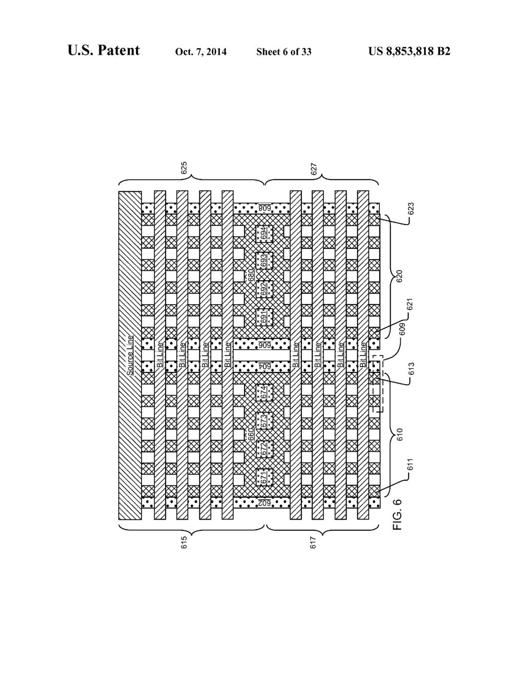
39 prise multilayer dielectric charge trapping structures known from flash memory technologies known in the art as SONOS, BE-SONOS, TANOS, and MA BE-SONOS. FIG.9 is a simplified block diagram of an integrated circuit according to an embodiment of the present invention. In the example shown in FIG. 9, the integrated circuit 975 includes a double-gate vertical channel memory array 960 (DGVC) implemented with one or both of the source line structures and silicide formations on word line structures, as described herein, on a integrated circuit substrate. A row decoder961 is coupled to a plurality of word lines 962, and arranged along rows in the memory array 960. A column decoder 963 is coupled to a plurality of bit lines 964 (or SSL lines as described above) arranged along columns in the memory array 960 for reading and programming data from the memory cells in the memory array 960. A plane decoder 958 is coupled to a plurality of planes in the memory array 960 on SSL lines 959 (orbit lines as described above). Addresses are supplied on bus 965 to column decoder 963, row decoder961 and plane decoder 958. Sense amplifiers and data-in struc tures in block 966 are coupled to the column decoder 963 in this example via data bus 967. Data is supplied via the data-in line 971 from input/output ports on the integrated circuit 975 or from other data sources internal or external to the inte grated circuit 975, to the data-instructures in block966. In the illustrated embodiment, other circuitry 974 is included on the integrated circuit, such as a general purpose processor or special purpose application circuitry, or a combination of modules providing system-on-a-chip functionality Supported by the programmable resistance cell array. Data is Supplied via the data-out line 972 from the sense amplifiers in block 966 to input/output ports on the integrated circuit 975, or to other data destinations internal or external to the integrated circuit 975. A controller implemented in this example using bias arrangement state machine 969 controls the application of bias arrangement Supply Voltage generated or provided through the voltage supply or supplies in block 968, such as read and program Voltages. The controller can be imple mented using special-purpose logic circuitry as known in the art. In alternative embodiments, the controller comprises a general-purpose processor, which can be implemented on the same integrated circuit, which executes a computer program to control the operations of the device. In yet other embodi ments, a combination of special-purpose logic circuitry and a general-purpose processor can be utilized for implementation of the controller. FIG. 10 is a flow chart illustrating a method for manufac turing a memory device. The method includes identifying areas on a substrate for formation of 3D memory blocks having a structure like that of FIG. 1. For each area, the method includes forming assist gate conductors by implant ing assistgate wells in the Substrate, or by patterning conduc tive material on the Substrate. Over the assistgate conductors, a layer of assist gate dielectric, Such as silicon dioxide is formed (block 1009). Over the insulating layer, the process includes forming a plurality of layers of a first conductive material separated by insulating material (block 1010), and etching the plurality of layers to define a plurality of stacks of conductive strips (block 1020). The stacks includes at least a bottom plane (GSL) of conductive strips, a plurality of inter mediate planes (WLS) of conductive strips, and a top plane of conductive strips (SSLs). The method includes forming a memory layer on side surfaces of conductive strips in the plurality of stacks (block 1030). The memory layer contacts side surfaces of the plu rality of conductive strips. The method includes forming a US 8,853,818 B layer of a second conductive material over and having a surface conformal with the memory layer on the plurality of stacks (block 1040). The method includes etching the layer of second conduc tive material to define a plurality of bit line structures (block 1050) arranged orthogonally over, and having Surfaces con formal with, the plurality of stacks. The bit line structures include inter-stack semiconductor body elements between the stacks and linking elements over the stacks connecting the inter-stack semiconductor body elements. The step of etching the layer of second conductive material (block1050) is also used in this example, to define at least one reference line structure (block 1050) arranged orthogonally over the plurality of stacks. The reference line structure includes inter-stack vertical conductive elements between the stacks in electrical communication with the layer of common Source conductor material. Also, the reference line structure can include linking elements over the stacks connecting the inter-stack vertical conductive elements. The step of etching the layer of second conductive material stops at a level above the layer of assistgate dielectric Such that portions of the layer of second conductive material below the level remain to form a reference conductor. The reference conductor is connected to the reference line structure and the bit line structures to allow electrical communication from the reference line struc ture to the bit line structures (block 1050). As a result of forming the bit line structures, memory cells are formed in interface regions at cross-points between side surfaces of the conductive strips in the plurality of interme diate planes (WLS) in the stacks and the inter-stack semicon ductor body elements of the plurality of bit line structures. Also, string select switches are disposed at interface regions with the top plane of conductive strips (SSLs), and reference select Switches are disposed at interface regions with the bottom plane (GSL) of conductive strips. The memory layer can comprise dielectric layers that can act as the gate dielec tric layers for the string select switches and reference select Switches. In one embodiment, the method can include implanting N-- doping material, with a first energy level, on the linking elements in the plurality of bit line structures, the reference conductor, and the linking elements in the at least one refer ence line structure (block 1060). The method can further include implanting N-- doping material, with a second energy level, on the inter-stack vertical conductive elements of the at least one reference line structure (block 1060), wherein the second energy level is higher than the first energy level. The inter-stack vertical conductive elements in the at least one reference line structure can have a larger cross-sectional area than the inter-stack semiconductor body elements in the bit line structures, as illustrated in FIG. 2. In one embodiment, the step of etching the plurality of layers to define a plurality of Stacks of conductive Strips (block 1020) in the method can include forming linking ele ments connecting sets of word lines in the intermediate planes (WL) as part of a decoding structure. The method further includes forming openings in the linking elements, and form ing interlayer connectors coupled to landing areas in the linking elements as another part of the decoding structure, where the interlayer connectors coupled to landing areas in lower intermediate planes extend through the openings in the linking elements (block 1070). The step of etching the plurality of layers to define a plu rality of stacks of conductive strips (block 1020) in the method can further include forming linking elements con necting sets of ground selection lines in the bottom plane. The method further includes forming interlayer connectors
.")
40 11 coupled to landing areas in the linking elements in the bottom plane, where the interlayer connectors extend through the openings in the linking elements in the intermediate planes (WLS) (block 1070). In one embodiment, a group of bit lines in the bit line structures and at least a source line in the at least one reference line structure are arranged orthogonally over a first set of word lines in the intermediate planes (WL), and a second adjacent set of word lines in the intermediate planes (WL), and the interlayer connectors for the first set are arranged on a side of the group parallel to the bit lines in the group, and the interlayer connectors for the second set are arranged on the same side of the group. In an alternative embodiment, a group of bit lines in the bit line structures and at least a source line in the at least one reference line structure are arranged orthogonally over a first set of word lines in the intermediate planes (WL), and a second adjacent set of word lines in the intermediate planes (WL), and the interlayer connectors for the first set are arranged on a side of the group parallel to the bit lines in the group, and the interlayer connectors for the second set are arranged on an opposing side of the group. In one embodiment, the method can include forming blocks that include linking elements connecting sets of word lines in the intermediate planes (WLS), and interlayer con nectors coupled to landing areas in the linking elements, where ends of the word lines in adjacent blocks are connected via the linking elements, and the linking elements include openings through which interlayer connecters coupled to landing areas in lower intermediate planes extend. The method can further include forming sidewall silicide forma tions on at least one side of adjacent blocks parallel to word lines in the adjacent blocks. In an alternative embodiment, the method can include forming pairs of adjacent stacks in the plurality of Stacks of conductive strips, wherein charge storage structures are dis posed in interface regions at cross-points between side Sur faces of a first side of word lines in the intermediate planes (WLS) and the inter-stack semiconductor body elements in the plurality of bit line structures. The method can further include forming sidewall silicide formations on side Surfaces of a second side of the word lines opposite the first side in the intermediate planes (WLS) of conductive strips in the pairs of adjacent stacks. The method can further include forming a first overlying conductive layer connected to the plurality of bit line struc tures, including a plurality of global bit lines coupled to sensing circuits, and forming a second overlying conductive layer connected to the at least one reference line structure, coupled to a reference voltage source (block 1080). FIGS. 11 through 18 illustrate an example process flow for a double-gate vertical channel structure. FIG. 11 illustrates a stage of the process flow after forming an assist gate conduc tor 1101, and a plurality of layers of a first conductive mate rial, such as layers 1110, 1120, 1130 and 1140, separated by layers of insulating material 1105, on an integrated circuit Substrate (not shown). FIG. 12 illustrates a stage of the process flow after etching the plurality of layers, and stopping at the assist gate conduc tor 1101, to define a plurality of stacks of conductive strips, including stacks 1210, 1211 and The stacks 1210, 1211 and 1212 include at least a bottom plane (GSL) of conductive strips, a plurality of intermediate planes (WLS) of conductive strips, and a top plane of conductive strips (SSLS). The plu rality of intermediate planes can include N planes, ranging from 0 to N-1, as illustrated in FIG. 12, for the stack Although not shown, the conductive strips are linked by pads US 8,853,818 B defined in the pattern used foretching the stacks. The pads can be used to form linking elements, like those of FIGS. 4 and 5 above, in Subsequent steps. FIG. 13 illustrates a stage of the process flow after forming a memory layer 1310 over and on sides of conductive strips in the plurality of stacks, including the stack The memory layer 1310 contacts side surfaces of the plurality of conduc tive strips. The memory layer 1310 can comprise a multli layer, dielectric charge storage structure as discussed above. FIG. 14 illustrates a stage of the process flow after forming a layer of a second conductive material 1410 over, and having a surface conformal with, the memory layer 1310 on the plurality of stacks, including the stack The second conductive material comprises a semiconductor adapted at least in the regions between the stacks, to act as channel regions for vertical strings of memory cells. FIG. 15 illustrates a stage of the process flow after a pat terned and timed etch of the layer of second conductive mate rial 1410, which is timed to stop before reaching the memory layer 1310 between the stacks, so that a reference conductor (e.g. 1560) is formed between each stack. Other processes to stop the etching in order to form the reference conductor can be used as well, including the use of an etch stop layer, disposed in the second conductor material in the trenches at the desired depth. The pattern of the etch defines a plurality of bit line structures 1520/1530 arranged orthogonally over, and having Surfaces conformal with, the plurality of Stacks, including the stack The bit line structures 1520/1530 include inter-stack semiconductor body elements 1520 between the stacks extending to the reference conductors (e.g. 1560), and linking elements 1530 over the stacks con necting the semiconductor body elements To reveal underlying structure, the illustration shows openings between the conductive strips in the stacks, in the regions between the bit line structures. However, these openings will be filled with an insulating material between the strips in the stacks. The step of etching the layer of second conductive material also defines at least one reference line structure 1540/1550, arranged orthogonally over the plurality of Stacks. The refer ence line structure includes inter-stack vertical conductive elements 1540 extending to the reference conductor (e.g., 1560) between the stacks and linking elements 1550 over the stacks connecting the inter-stack vertical conductive ele ments FIG. 15 illustrates that the reference conductor 1560 left as a result of the patterned, timed etch is disposed between the bottom plane (GSL) of conductive strips and the assist gate structure 1101 on the substrate. The memory layer 1310 can act as an assist gate dielectric between the reference conductor 1560 and the assist gate conductor 1101 FIG. 16 illustrates a stage of the process flow after the bit line structures are formed, where the process includes implanting N-- doping material in the direction shown by arrows 1610, with a first energy level, on the linking elements 1530 in the plurality of bit line structures, the reference con ductor 1560 in exposed areas between the bit line structures, and between the bit line structure and the reference line struc ture, and the linking elements 1550 in the at least one refer ence line structure. The first energy level can be less than 30 kev, with a typical dose around 1E14 per cm. If the profile of the inter-stack semiconductor body ele ments 1520 of the bit line structures is sufficiently vertical (nearly 90 degrees) to the reference conductor 1560, side walls of the inter-stack semiconductor body elements 1520 of the bit line structures receive a minimal amount of the N+ doping material with the first energy level, while most of the

41 13 N+ doping material is implanted into the reference conductor 1560, reducing its resistance accordingly. FIG. 17 illustrates a stage of the process flow following the implant of FIG. 16, where the process flow includes an addi tional step of implanting N-- doping material in the direction shown by arrow 1710, with a second energy level, on the inter-stack vertical conductive elements 1540 of the at least one reference line structure, wherein the second energy level is higher than the first energy level. For instance, the second energy level can be around 30 to 50 kev, with a typical dose around 1E14 to 1E15 per cm. An implant mask (not shown) can be used to protect the bit line structures and other parts of the memory array from this additional step of implanting. This can improve the conductivity of the inter-stack vertical conductive elements 1540 for the reference line structure. The inter-stack vertical conductive elements 1540 in the at least one reference line structure can have a larger cross sectional area than the inter-stack semiconductor body ele ments 1520 in the bit line structures, as illustrated in FIG. 2. FIG. 18 illustrates a stage of the process flow following a staircase etching process used to isolate the individual SSL lines, and to form linking elements 1861, 1862, 1863 coupled to the conductive strips in the plurality of stacks that include landing areas for interlayer connectors 1871, 1872, The pads used for linking elements 1861, 1862, 1863 can be patterned at the same time that the Stacks are patterned (See, FIG. 12). In one embodiment, as illustrated in FIG. 4, a group 430 of bit lines in the bit line structures and at least a linking element 440 in the at least one reference line structure are arranged orthogonally over a first set 410 of word lines in the interme diate planes (WL), and a second adjacent set 420 of word lines in the intermediate planes (WL), and interlayer connectors 471 through 474 for the first set 410 are arranged on a side of the group 430 parallel to the bit lines in the group 430, and interlayer connectors 491 through 492 for the second set 420 are arranged on the same side of the group 430. In an alternative embodiment, as illustrated by FIG. 5, a group 530 of linking elements 531 through 538 in the bit line structures and at least a linking element 540 in the at least one reference line structure are arranged orthogonally over a first set 510 of word lines in the intermediate planes (WL), and a second adjacent set 520 of word lines in the intermediate planes (WL), and interlayer connectors 571 through 574 for the first set 510 are arranged on a side of the group 530 parallel to the bit lines in the group 530, and interlayer connectors 591 through 594 for the second set 520 are arranged on an oppos ing side of the group 530. In one embodiment, the process flow can include forming blocks that include linking elements connecting sets of word lines in the intermediate planes (WLS), and interlayer con nectors coupled to landing areas in the linking elements, where ends of the word lines in adjacent blocks are connected via the linking elements, and the linking elements include openings through which interlayer connecters coupled to landing areas in lower intermediate planes extend. The pro cess flow can further include forming sidewall silicide forma tions on at least one side of adjacent blocks parallel to word lines in the adjacent blocks. Sidewall silicide formations can be CoSi (cobalt silicide), TiSi (titanium silicide), or other silicide compounds, made for example using SAlicide (self aligned silicide) processes on sidewalls of sets of word lines. FIGS. 19 through 24 illustrate an example process flow for an embodiment in a sidewall silicide formation in a vertical channel structure. FIG. 19 is a cross-section taken orthogo nally to the conductive strips in a structure like that of FIG. 11, including the intermediate planes of conductive strips 1930, US 8,853,818 B , 1950, 1960 (WL and WL) separated by insulating material 1905, after a word line slit process. The slit process can be a patterned etch used to cut conductive strips into multiple sets of word lines, exposing sidewalls of the inter mediate planes WL and WL. FIG. 19 illustrates a first set of word lines 1910, a second set of word lines 1920, and a space 1915 between the two sets, where individual word lines are to be formed. Although the top plane of conductive strips (SSLs) and the bottom plane (GSL) of conductive strips are not shown in FIGS. 19 through 24, the process flow can include forming a sidewall silicide formation on a side of a set of string selection lines in the top plane, and on a side of a set of ground selection lines in the bottom plane. FIG. 20 illustrates a stage in the process after a procedure to form silicide on the exposed sides between the conductive strips 1930, 1940, 1950, 1960, while preventing silicide for mation on the opposing sides. The silicide can be formed by depositing a thin silicide precursor, Such as a transition metal layer 2090 over sidewalls of the two sets of word lines. Then the structure is annealed, causing the silicide precursor to react with the conductive material in the intermediate planes WL and WL to form low-resistance sidewall silicide for mations, such as sidewall silicide formations 1939 and 1959 for the first set of word lines 1910, and sidewall silicide formations 1941 and 1961 for the second set of word lines As shown in FIG. 21, after the reaction to form the sidewall silicide formations 1939, 1959, 1941 and 1961, remaining or excess transition metal is etched away. FIG. 22 illustrates a stage in the process after etching the plurality of layers to divide the conductive strips 1930, 1940, 1950, 1960, forming divided strips 1931, 1933, 1943, 1945, 1951, 1953, 1963, and The divided strips define a plurality of Stacks of conductive strips, such as stacks 2210 and 2220 for the first set of word lines 1910, and stacks 2230 and 2240 for the second set of word lines The stacks include at least a bottom plane (GSL) of conductive strips (not shown), a plurality of intermediate planes (WLS) of conduc tive strips, and a top plane of conductive strips (SSLS) (not shown). The plurality of intermediate planes can include N planes, ranging from 0 to N-1. FIG. 23 illustrates a stage in the process after forming a memory layer 2390 on side surfaces of conductive strips in the plurality of stacks, in regions not covered by the sidewall silicide formations 1939, 1959, 1941 and The memory layer 2390 contacts side surfaces of the plurality of conduc tive strips. FIG. 24 illustrates a stage in the process after forming a layer of a second conductive material to form a vertical inter stack semiconductor body element 2490 over, and having a surface conformal with, the memory layer 2390 on the plu rality of stacks. The space 1915 between the two sets of word lines is filled with insulation material 2480 at some position in the process flow. A double-gate, flash memory cell (region 2395) results at a cross-point of the conductive strips 1951 and 1953 with the vertical inter-stack semiconductor body element 2490 of the bit line structure, and at other similar cross-points to form a 3D memory array. The process flow can then continue as described with reference to FIG. 15 to etch the layer of second conductive material, and so on. FIGS. 25 through 33 illustrate an example process flow for an alternative embodiment in a sidewall silicide formation in a vertical channel structure. In the alternative embodiment, charge storage structures are disposed in interface regions at cross-points between side surfaces of a first side of word lines in the intermediate planes (WLS) and the inter-stack semicon ductor body elements in the plurality of bit line structures, and

42 15 sidewall silicide formations are disposed on side surfaces of a second side of the word lines opposite the first side in the intermediate planes (WLS) of conductive strips in the pairs of adjacent stacks. FIG. 25 illustrates a cross-section of a par tially fabricated memory device. In the example shown in FIG. 25, the memory device includes a reference conductor layer 2501, and a plurality of sacrificial layers, including sacrificial layers 2510, 2520, 2530 and 2540, separated by insulating material FIG. 26 illustrates a stage in the process after etching the plurality of sacrificial layers to define a plurality of pairs of adjacent stacks, by forming openings 2691 and 2692 etched through the plurality of sacrificial layers. The openings 2691 and 2692 are used to form the inter-stack semiconductor body elements shared by the pairs of adjacent stacks. FIG. 27 illustrates a stage in the process after forming the inter-stack semiconductor body elements 2791 and 2792 in openings 2691 and 2692, respectively, using the second con ductive material, and etching openings, such as an opening 2790 extending to the reference conductor layer 2501, to expose sacrificial layers 2510, 2520, 2530 and 2540, and to separate pairs of adjacent stacks. FIG. 28 illustrates a stage in the process after removing sacrificial layers 2510, 2520, 2530 and 2540 exposed by the openings such as the opening This etch process leaves layers of insulating material 2505 in the respective stacks adhered to the second conductive material that acts as the inter-stack semiconductor body elements, with openings (e.g. 2801) in between. FIG. 29 illustrates a stage in the process after forming a memory layer 2990 on side surfaces of the inter-stack semi conductor body elements 2791 and The memory layer 2990 can include a multilayer dielectric charge storage struc ture, known from flash memory technologies, including for example flash memory technologies known as SONOS, BE SONOS, TANOS, and MA BE-SONOS. FIG. 30 illustrates a stage in the process after forming a plurality of layers of the first conductive material 3090 between and over pairs of adjacent stacks, filling the openings left by removal of the sacrificial layers between layers of insulating material 2505, and over the memory layer FIG. 31 illustrates a stage in the process after etching trenches (e.g. 3101) between the stacks of conductive strips, removing excess material in the layers of the first conductive material 3090 to define stacks including at least a bottom plane (GSL) of conductive strips 3111,3113,3115, and 3117, a plurality of intermediate planes (WLS) of conductive strips 3121, 3123, 3125, and 3127, and conductive strips 3131, 3133, 3135, and 3137, and a top plane of conductive strips (SSLs)3141, 3143, 3145, and FIG. 32 illustrates a stage in the process after a process to form silicide on the sidewalls of the conductive strips , 3115, and 3117, 3121, 3123, 3125, and 3127, 3131, 3133, 3135, and 3137, and 3141, 3143, 3145, and 3147, where the conductive strips comprise a silicon-containing material. The silicide process includes depositing a thin sili cide precursor, such as a transition metal layer 3290, over sidewalls of the pairs of adjacent stacks. The silicide precur sor is then annealed, to cause it to react with the silicon in the conductive strips 3111, 3113, 3115, and 3117, 3121, 3123, 3125, and 3127,3131,3133,3135, and 3137, and 3141,3143, 3145, and 3147, to form low-resistance sidewall silicide for mations, such as sidewall silicide formations 3122., 3124, 3126, and 3128, silicide formations 3132, 3134, 3136, and 3138, and sidewall silicide formations 3142,3144,3146, and 3148, and sidewall silicide formations 3112,3114,3116, and US 8,853,818 B FIG.33 illustrates a stage in the process after etching away any excess silicide precursor. The manufacturing process continues as described above, for example, to complete a 3D memory array, with dual-gate vertical NAND strings. While the present invention is disclosed by reference to the preferred embodiments and examples detailed above, it is to be understood that these examples are intended in an illustra tive rather than in a limiting sense. It is contemplated that modifications and combinations will readily occur to those skilled in the art, which modifications and combinations will be within the spirit of the invention and the scope of the following claims. What is claimed is: 1. A memory device including an array of NAND strings of memory cells, comprising: an integrated circuit Substrate; a plurality of stacks of conductive strips separated by insu lating material, including at least a bottom plane (GSL) of conductive strips, a plurality of intermediate planes (WLS) of conductive strips, and a top plane of conduc tive strips (SSLs); a plurality of bit line structures arranged orthogonally over, and having Surfaces conformal with, the plurality of stacks, including inter-stack semiconductor body ele ments between the stacks, and linking elements over the stacks connecting the inter-stack semiconductor body elements; charge storage structures in interface regions at cross points between side surfaces of the conductive strips in the stacks and inter-stack semiconductor body elements of the plurality of bit line structures: at least one reference line structure arranged orthogonally over the plurality of stacks, including inter-stack vertical conductive elements between the stacks, and linking elements over the stacks connecting the inter-stack Ver tical conductive elements; and sidewall silicide formations disposed on side Surfaces of a side of at least one of the conductive strips in the stacks opposite a second side of the at least one of the conduc tive strips, wherein on the side surfaces of the second side the charge storage structures are formed. 2. The memory device of claim 1, further comprising: blocks including linking elements connecting sets of word lines in the intermediate planes (WLS), and interlayer connectors coupled to landing areas in the linking ele ments, wherein ends of the word lines in adjacent blocks are connected via the linking elements, and the linking elements include openings through which interlayer connecters coupled to landing areas in lower intermedi ate planes extend; and sidewall silicide formations disposed on at least one side of adjacent blocks parallel to word lines in the adjacent blocks. 3. The memory device of claim 1, further comprising: pairs of adjacent stacks in the plurality of stacks of con ductive strips, wherein charge storage structures are dis posed in interface regions at cross-points between side surfaces of a first side of word lines in the intermediate planes (WLS) and the inter-stack semiconductor body elements in the plurality of bit line structures; and sidewall silicide formations disposed on side Surfaces of a second side of the word lines opposite the first side in the intermediate planes (WLS) of conductive strips in the pairs of adjacent stacks. 4. The memory device of claim 1, wherein a group of linking elements in the bit line structures and at least a linking element in the at least one reference line structure are

43 17 arranged orthogonally over a first set of word lines in the intermediate planes (WL), and a second adjacent set of word lines in the intermediate planes (WL), and interlayer connec tors for the first set are arranged on a side of the group parallel to the bit lines in the group, and interlayer connectors for the second set are arranged on the same side of the group. 5. The memory device of claim 1, wherein a group of linking elements in the bit line structures and at least a linking element in the at least one reference line structure are arranged orthogonally over a first set of word lines in the intermediate planes (WL), and a second adjacent set of word lines in the intermediate planes (WL), and interlayer connec tors for the first set are arranged on a side of the group parallel to the bit lines in the group, and interlayer connectors for the second set are arranged on an opposing side of the group. 6. A memory device including an array of NAND strings of memory cells, comprising: an integrated circuit Substrate; a plurality of stacks of conductive strips separated by insu lating material, including at least a bottom plane (GSL) of conductive strips, a plurality of intermediate planes (WLS) of conductive strips, and a top plane of conduc tive strips (SSLs); a reference conductor (CS) disposed in a level between the bottom plane of conductive strips and the integrated circuit Substrate; a plurality of bit line structures arranged orthogonally over, and having Surfaces conformal with, the plurality of stacks, including inter-stack semiconductor body ele ments between the stacks connected to the reference conductor, and linking elements over the stacks connect ing the inter-stack semiconductor body elements; charge storage structures in interface regions at cross points between side surfaces of the conductive strips in the plurality of intermediate planes in the stacks and the inter-stack semiconductor body elements of the plurality of bit line structures; at least one reference line structure arranged orthogonally over the plurality of stacks, including inter-stack vertical conductive elements between the stacks connected to the reference conductor, and linking elements over the stacks connecting the inter-stack vertical conductive ele ments, the inter-stack vertical conductive elements hav ing a higher conductivity than the inter-stack semicon ductor body elements; and string select Switches at interface regions with the top plane of conductive strips, and reference select Switches at interface regions with the bottom plane of conductive strips. 7. The memory device of claim 6, further comprising: blocks including linking elements connecting sets of word lines in the intermediate planes (WLS), and interlayer connectors coupled to landing areas in the linking ele ments, wherein ends of the word lines in adjacent blocks are connected via the linking elements, and the linking elements include openings through which interlayer connecters coupled to landing areas in lower intermedi ate planes extend; and sidewall silicide formations disposed on at least one side of adjacent blocks parallel to word lines in the adjacent blocks. US 8,853,818 B The memory device of claim 6, further comprising: pairs of adjacent stacks in the plurality of stacks of con ductive strips, wherein charge storage structures are dis posed in interface regions at cross-points between side surfaces of a first side of word lines in the intermediate planes (WLS) and the inter-stack semiconductor body elements in the plurality of bit line structures; and sidewall silicide formations disposed on side Surfaces of a second side of the word lines opposite the first side in the intermediate planes (WLS) of conductive strips in the pairs of adjacent stacks. 9. The memory device of claim 6, including a first overly ing conductive layer connected to the plurality of bit line structures, including a plurality of global bit lines coupled to sensing circuits. 10. The memory device of claim 6, including a second overlying conductive layer connected to the at least one ref erence line structure, coupled to a reference Voltage source. 11. The memory device of claim 6, wherein the reference conductor includes N+ doped semiconductor material, and the linking elements of the at least one reference line structure include N-- doped semiconductor material. 12. The memory device of claim 6, wherein the inter-stack vertical conductive elements of the at least one reference line structure include N-- doped semiconductor material. 13. The memory device of claim 6, wherein the inter-stack vertical conductive elements in the at least one reference line structure have a larger cross-sectional area than the inter stack semiconductor body elements in the bit line structures. 14. The memory device of claim 6, further comprising: linking elements connecting sets of word lines in the inter mediate planes (WLs); and interlayer connectors coupled to landing areas in the link ing elements, wherein the linking elements include openings through which interlayer connectors coupled to landing areas in lower intermediate planes extend. 15. The memory device of claim 14, further comprising: linking elements connecting sets of ground selection lines in the bottom plane (GSL); and interlayer connectors coupled to landing areas in the link ing elements in the bottom plane, wherein the interlayer connectors extend through the openings in the linking elements in the intermediate planes (WLS). 16. The memory device of claim 14, wherein a group of linking elements in the bit line structures and at least a linking element in the at least one reference line structure are arranged orthogonally over a first set of word lines in the intermediate planes (WL), and a second adjacent set of word lines in the intermediate planes (WL), and the interlayer connectors for the first set are arranged on a side of the group parallel to the bit lines in the group, and the interlayer con nectors for the second set are arranged on the same side of the group. 17. The memory device of claim 14, wherein a group of linking elements in the bit line structures and at least a linking element in the at least one reference line structure are arranged orthogonally over a first set of word lines in the intermediate planes (WL), and a second adjacent set of word lines in the intermediate planes (WL), and the interlayer connectors for the first set are arranged on a side of the group parallel to the bit lines in the group, and the interlayer con nectors for the second set are arranged on an opposing side of the group.
(12) United States Patent (10) Patent No.: US 7,763,928 B2
 United States Patent (10) Patent No.: US 7,763,928 B2") USOO7763928B2 (12) United States Patent (10) Patent No.: Lin et al. (45) Date of Patent: Jul. 27, 2010 (54) MULTI-TIME PROGRAMMABLE MEMORY (58) Field of Classification Search... 257/314321, 257/E29.129,
USOO7763928B2 (12) United States Patent (10) Patent No.: Lin et al. (45) Date of Patent: Jul. 27, 2010 (54) MULTI-TIME PROGRAMMABLE MEMORY (58) Field of Classification Search... 257/314321, 257/E29.129,
(12) Patent Application Publication (10) Pub. No.: US 2009/ A1
 Patent Application Publication (10) Pub. No.: US 2009/ A1") (19) United States US 2009.0160019A1 (12) Patent Application Publication (10) Pub. o.: US 2009/0160019 A1 Yang (43) Pub. Date: Jun. 25, 2009 (54) SEMICODUCTOR CAPACITOR Publication Classification (51)
(19) United States US 2009.0160019A1 (12) Patent Application Publication (10) Pub. o.: US 2009/0160019 A1 Yang (43) Pub. Date: Jun. 25, 2009 (54) SEMICODUCTOR CAPACITOR Publication Classification (51)
(12) Patent Application Publication (10) Pub. No.: US 2001/ A1
 Patent Application Publication (10) Pub. No.: US 2001/ A1") US 2001 OO10407A1 (19) United States (12) Patent Application Publication (10) Pub. No.: US 2001/0010407 A1 Ker et al. (43) Pub. Date: (54) LOW-CAPACITANCE BONDING PAD FOR (30) Foreign Application Priority
US 2001 OO10407A1 (19) United States (12) Patent Application Publication (10) Pub. No.: US 2001/0010407 A1 Ker et al. (43) Pub. Date: (54) LOW-CAPACITANCE BONDING PAD FOR (30) Foreign Application Priority
(12) United States Patent
 United States Patent") USOO7777214B2 (12) United States Patent Shin et al. (10) Patent No.: (45) Date of Patent: US 7,777,214 B2 Aug. 17, 2010 (54) PHASE CHANGE MEMORY DEVICE WITH A NOVEL ELECTRODE (75) Inventors: Jae-Min Shin,
USOO7777214B2 (12) United States Patent Shin et al. (10) Patent No.: (45) Date of Patent: US 7,777,214 B2 Aug. 17, 2010 (54) PHASE CHANGE MEMORY DEVICE WITH A NOVEL ELECTRODE (75) Inventors: Jae-Min Shin,
(12) United States Patent (10) Patent No.: US 6,365,505 B1
 United States Patent (10) Patent No.: US 6,365,505 B1") USOO6365505B1 (12) United States Patent (10) Patent No.: US 6,365,505 B1 Wang et al. (45) Date of Patent: Apr. 2, 2002 (54) METHOD OF MAKING ASLOT VIA FILLED 6,127,258 A * 10/2000 Watanabe et al... 438/637
USOO6365505B1 (12) United States Patent (10) Patent No.: US 6,365,505 B1 Wang et al. (45) Date of Patent: Apr. 2, 2002 (54) METHOD OF MAKING ASLOT VIA FILLED 6,127,258 A * 10/2000 Watanabe et al... 438/637
(12) United States Patent
 United States Patent") USOO7335956B2 (12) United States Patent Chen et al. (10) Patent No.: (45) Date of Patent: Feb. 26, 2008 (54) (75) (73) (*) (21) (22) (65) (51) (52) (58) CAPACTOR DEVICE WITH VERTICALLY ARRANGED CAPACTOR
USOO7335956B2 (12) United States Patent Chen et al. (10) Patent No.: (45) Date of Patent: Feb. 26, 2008 (54) (75) (73) (*) (21) (22) (65) (51) (52) (58) CAPACTOR DEVICE WITH VERTICALLY ARRANGED CAPACTOR
(12) United States Patent
 United States Patent") USOO9633947B2 (12) United States Patent Jacob (10) Patent No.: (45) Date of Patent: Apr. 25, 2017 (54) (71) (72) (73) (*) (21) (22) (65) (51) (52) FOLDED BALLISTC CONDUCTOR INTERCONNECT LINE Applicant:
USOO9633947B2 (12) United States Patent Jacob (10) Patent No.: (45) Date of Patent: Apr. 25, 2017 (54) (71) (72) (73) (*) (21) (22) (65) (51) (52) FOLDED BALLISTC CONDUCTOR INTERCONNECT LINE Applicant:
(12) Patent Application Publication (10) Pub. No.: US 2013/ A1. LEE et al. (43) Pub. Date: Jan. 3, 2013
 Patent Application Publication (10) Pub. No.: US 2013/ A1. LEE et al. (43) Pub. Date: Jan. 3, 2013") US 2013 OOO1573A1 (19) United States (12) Patent Application Publication (10) Pub. No.: US 2013/0001573 A1 LEE et al. (43) Pub. Date: Jan. 3, 2013 (54) THIN FILM TRANSISTOR AND METHOD OF Publication Classification
US 2013 OOO1573A1 (19) United States (12) Patent Application Publication (10) Pub. No.: US 2013/0001573 A1 LEE et al. (43) Pub. Date: Jan. 3, 2013 (54) THIN FILM TRANSISTOR AND METHOD OF Publication Classification
(22) Filed: Feb. 22, 2000 Primary Examiner-Carl Whitehead, Jr. 30 F Application O O P tv Dat. ASSistant Examiner Toniae M. Thomas
 Filed: Feb. 22, 2000 Primary Examiner-Carl Whitehead, Jr. 30 F Application O O P tv Dat. ASSistant Examiner Toniae M. Thomas") (12) United States Patent Hwang et al. USOO6479343B1 (10) Patent No.: (45) Date of Patent: Nov. 12, 2002 (54) DRAM CELL CAPACITOR AND MANUFACTURING METHOD THEREOF (75) Inventors: Yoo-Sang Hwang, Suwon;
(12) United States Patent Hwang et al. USOO6479343B1 (10) Patent No.: (45) Date of Patent: Nov. 12, 2002 (54) DRAM CELL CAPACITOR AND MANUFACTURING METHOD THEREOF (75) Inventors: Yoo-Sang Hwang, Suwon;
Semiconductor Memories
 Semiconductor References: Adapted from: Digital Integrated Circuits: A Design Perspective, J. Rabaey UCB Principles of CMOS VLSI Design: A Systems Perspective, 2nd Ed., N. H. E. Weste and K. Eshraghian
(12) Patent Application Publication (10) Pub. No.: US 2013/ A1. Chang et al. (43) Pub. Date: Dec. 5, 2013
 Patent Application Publication (10) Pub. No.: US 2013/ A1. Chang et al. (43) Pub. Date: Dec. 5, 2013") (19) United States US 2013 0320422A1 (12) Patent Application Publication (10) Pub. No.: US 2013/0320422 A1 Chang et al. (43) Pub. Date: Dec. 5, 2013 (54) FINFET CONTACTING A CONDUCTIVE (52) U.S. Cl. STRAP
(19) United States US 2013 0320422A1 (12) Patent Application Publication (10) Pub. No.: US 2013/0320422 A1 Chang et al. (43) Pub. Date: Dec. 5, 2013 (54) FINFET CONTACTING A CONDUCTIVE (52) U.S. Cl. STRAP
GMU, ECE 680 Physical VLSI Design 1
 ECE680: Physical VLSI Design Chapter VIII Semiconductor Memory (chapter 12 in textbook) 1 Chapter Overview Memory Classification Memory Architectures The Memory Core Periphery Reliability Case Studies
USPC / 295. See application file for complete search history. Tso - Ping Ma, Branford, CT ( US )
") THI NA MATU U U U UTAWA DINI US009818848B2 ( 12 ) United States Patent Sun et al. ( 54 ) THREE - DIMENSIONAL FERROELECTRIC FET - BASED STRUCTURES ( 71 ) Applicant : Yale University, New Haven, CT ( US
THI NA MATU U U U UTAWA DINI US009818848B2 ( 12 ) United States Patent Sun et al. ( 54 ) THREE - DIMENSIONAL FERROELECTRIC FET - BASED STRUCTURES ( 71 ) Applicant : Yale University, New Haven, CT ( US
(12) Patent Application Publication (10) Pub. No.: US 2014/ A1
 Patent Application Publication (10) Pub. No.: US 2014/ A1") (19) United States US 20140216484A1 (12) Patent Application Publication (10) Pub. No.: US 2014/0216484 A1 Liu (43) Pub. Date: Aug. 7, 2014 (54) ELECTRONIC CIGARETTE (52) U.S. Cl. CPC... A24F 47/008 (2013.01)
(19) United States US 20140216484A1 (12) Patent Application Publication (10) Pub. No.: US 2014/0216484 A1 Liu (43) Pub. Date: Aug. 7, 2014 (54) ELECTRONIC CIGARETTE (52) U.S. Cl. CPC... A24F 47/008 (2013.01)
United States Patent (19) Gruaz et al.
 Gruaz et al.") United States Patent (19) Gruaz et al. (54) DEVICE FOR LOCATING AN OBJECT SITUATED CLOSE TO A DETECTION AREA AND A TRANSPARENT KEYBOARD USING SAID DEVICE 75 Inventors: Daniel Gruaz, Montigny le Bretonneux;
United States Patent (19) Gruaz et al. (54) DEVICE FOR LOCATING AN OBJECT SITUATED CLOSE TO A DETECTION AREA AND A TRANSPARENT KEYBOARD USING SAID DEVICE 75 Inventors: Daniel Gruaz, Montigny le Bretonneux;
Digital Integrated Circuits A Design Perspective. Semiconductor. Memories. Memories
 Digital Integrated Circuits A Design Perspective Semiconductor Chapter Overview Memory Classification Memory Architectures The Memory Core Periphery Reliability Case Studies Semiconductor Memory Classification
(12) Patent Application Publication (10) Pub. No.: US 2016/ A1
 Patent Application Publication (10) Pub. No.: US 2016/ A1") US 20160358915A1 (19) United States (12) Patent Application Publication (10) Pub. No.: US 2016/0358915 A1 Flachowsky et al. (43) Pub. Date: (54) FERROELECTRIC FINFET HOIL 29/5 (2006.01) HOIL 29/78 (2006.01)
US 20160358915A1 (19) United States (12) Patent Application Publication (10) Pub. No.: US 2016/0358915 A1 Flachowsky et al. (43) Pub. Date: (54) FERROELECTRIC FINFET HOIL 29/5 (2006.01) HOIL 29/78 (2006.01)
(ΐ2) United States Patent
 United States Patent") US009627440B2 US009627440B2 (ΐ2) United States Patent Russo et al. (ΐο) Patent No.: (4) Date of Patent: Apr. 18, 17 (4) PHASE CHANGE MEMORY APPARATUSES (71) Applicant: Micron Technology, Inc., Boise, ID
US009627440B2 US009627440B2 (ΐ2) United States Patent Russo et al. (ΐο) Patent No.: (4) Date of Patent: Apr. 18, 17 (4) PHASE CHANGE MEMORY APPARATUSES (71) Applicant: Micron Technology, Inc., Boise, ID
(12) Patent Application Publication (10) Pub. No.: US 2011/ A1
 Patent Application Publication (10) Pub. No.: US 2011/ A1") (19) United States US 20110248723A1 (12) Patent Application Publication (10) Pub. No.: US 2011/0248723 A1 YEH et al. (43) Pub. Date: Oct. 13, 2011 (54) CAPACITIVE SENSOR HAVING CALIBRATION MECHANISMAND
(19) United States US 20110248723A1 (12) Patent Application Publication (10) Pub. No.: US 2011/0248723 A1 YEH et al. (43) Pub. Date: Oct. 13, 2011 (54) CAPACITIVE SENSOR HAVING CALIBRATION MECHANISMAND
(12) Patent Application Publication (10) Pub. No.: US 2016/ A1
 Patent Application Publication (10) Pub. No.: US 2016/ A1") (19) United States US 2016O133638A1 (12) Patent Application Publication (10) Pub. No.: US 2016/0133638A1 Simsek-Ege et al. (43) Pub. Date: May 12, 2016 (54) (71) (72) (21) (22) MEMORY CELL, PLLAR INCLUDING
(19) United States US 2016O133638A1 (12) Patent Application Publication (10) Pub. No.: US 2016/0133638A1 Simsek-Ege et al. (43) Pub. Date: May 12, 2016 (54) (71) (72) (21) (22) MEMORY CELL, PLLAR INCLUDING
(12) United States Patent
 United States Patent") USOO7310217B2 (12) United States Patent Takashima et al. (10) Patent No.: (45) Date of Patent: US 7,310,217 B2 Dec. 18, 2007 (54) MONOLITHIC CAPACITOR AND MOUNTING STRUCTURE THEREOF (75) Inventors: Hirokazu
USOO7310217B2 (12) United States Patent Takashima et al. (10) Patent No.: (45) Date of Patent: US 7,310,217 B2 Dec. 18, 2007 (54) MONOLITHIC CAPACITOR AND MOUNTING STRUCTURE THEREOF (75) Inventors: Hirokazu
(12) United States Patent
 United States Patent") (12) United States Patent US007191654B2 (10) Patent No.: US 7,191,654 B2 Dwyer et al. (45) Date of Patent: Mar. 20, 2007 (54) METHODS AND SYSTEMS FOR ADJUSTING (56) References Cited MAGNETIC RETURN PATH
(12) United States Patent US007191654B2 (10) Patent No.: US 7,191,654 B2 Dwyer et al. (45) Date of Patent: Mar. 20, 2007 (54) METHODS AND SYSTEMS FOR ADJUSTING (56) References Cited MAGNETIC RETURN PATH
Lecture 25. Semiconductor Memories. Issues in Memory
 Lecture 25 Semiconductor Memories Issues in Memory Memory Classification Memory Architectures TheMemoryCore Periphery 1 Semiconductor Memory Classification RWM NVRWM ROM Random Access Non-Random Access
Digital Integrated Circuits A Design Perspective
 Semiconductor Memories Adapted from Chapter 12 of Digital Integrated Circuits A Design Perspective Jan M. Rabaey et al. Copyright 2003 Prentice Hall/Pearson Outline Memory Classification Memory Architectures
(12) United States Patent (10) Patent No.: US 9,153,764 B2. Colli (45) Date of Patent: Oct. 6, 2015
 United States Patent (10) Patent No.: US 9,153,764 B2. Colli (45) Date of Patent: Oct. 6, 2015") US009 153764B2 (12) United States Patent (10) Patent No.: US 9,153,764 B2 Colli (45) Date of Patent: Oct. 6, 2015 (54) APPARATUS FORTRANSDUCING A 386 A. ck 33. Sarah al..............3s. aghloul et al....
US009 153764B2 (12) United States Patent (10) Patent No.: US 9,153,764 B2 Colli (45) Date of Patent: Oct. 6, 2015 (54) APPARATUS FORTRANSDUCING A 386 A. ck 33. Sarah al..............3s. aghloul et al....
US 9,214,722 B2 Dec. 15, 2015
 I lllll llllllll Ill lllll lllll lllll lllll lllll 111111111111111111111111111111111 US009214 722B2 c12) United States Patent Georgakopoulos et al. (IO) Patent No.: (45) Date of Patent: US 9,214,722 B2
(12) Patent Application Publication (10) Pub. No.: US 2009/ A1
 Patent Application Publication (10) Pub. No.: US 2009/ A1") (19) United States US 20090009193A1 (12) Patent Application Publication (10) Pub. No.: US 2009/0009193 A1 Hsiung et al. (43) Pub. Date: Jan. 8, 2009 (54) MOISTURE-SENSITIVE ELEMENT WITH AN INTERDIGITAL
(19) United States US 20090009193A1 (12) Patent Application Publication (10) Pub. No.: US 2009/0009193 A1 Hsiung et al. (43) Pub. Date: Jan. 8, 2009 (54) MOISTURE-SENSITIVE ELEMENT WITH AN INTERDIGITAL
(12) Patent Application Publication (10) Pub. No.: US 2016/ A1
 Patent Application Publication (10) Pub. No.: US 2016/ A1") (19) United States US 2016O247659A1 (12) Patent Application Publication (10) Pub. No.: US 2016/0247659 A1 OH et al. (43) Pub. Date: Aug. 25, 2016 (54) ELECTROSTATIC QUADRUPOLE Publication Classification
(19) United States US 2016O247659A1 (12) Patent Application Publication (10) Pub. No.: US 2016/0247659 A1 OH et al. (43) Pub. Date: Aug. 25, 2016 (54) ELECTROSTATIC QUADRUPOLE Publication Classification
(12) Patent Application Publication (10) Pub. No.: US 2014/ A1
 Patent Application Publication (10) Pub. No.: US 2014/ A1") (19) United States US 20140238873A1 (12) Patent Application Publication (10) Pub. No.: US 2014/0238873 A1 Li et al. (43) Pub. Date: Aug. 28, 2014 (54) MODIFIED BUBBLING TRANSFER METHOD (52) U.S. Cl. FOR
(19) United States US 20140238873A1 (12) Patent Application Publication (10) Pub. No.: US 2014/0238873 A1 Li et al. (43) Pub. Date: Aug. 28, 2014 (54) MODIFIED BUBBLING TRANSFER METHOD (52) U.S. Cl. FOR
SEMICONDUCTOR MEMORIES
 SEMICONDUCTOR MEMORIES Semiconductor Memory Classification RWM NVRWM ROM Random Access Non-Random Access EPROM E 2 PROM Mask-Programmed Programmable (PROM) SRAM FIFO FLASH DRAM LIFO Shift Register CAM
(12) United States Patent
 United States Patent") USOO743665OB2 (12) United States Patent Oguni et al. (10) Patent No.: (45) Date of Patent: US 7.436,650 B2 Oct. 14, 2008 (54) LAMINATED CERAMIC CAPACITOR (75) Inventors: Toshimi Oguni, Izumo (JP); Hiroyuki
USOO743665OB2 (12) United States Patent Oguni et al. (10) Patent No.: (45) Date of Patent: US 7.436,650 B2 Oct. 14, 2008 (54) LAMINATED CERAMIC CAPACITOR (75) Inventors: Toshimi Oguni, Izumo (JP); Hiroyuki
United States Patent (19)
") United States Patent (19) Rodov 54 METHOD OF MANUFACTURE OF ZENER DODES (75 Inventor: Vladimir Rodov, Los Angeles, Calif. 73) Assignee: International Rectifier Corporation, Los Angeles, Calif. 21 Appl.
United States Patent (19) Rodov 54 METHOD OF MANUFACTURE OF ZENER DODES (75 Inventor: Vladimir Rodov, Los Angeles, Calif. 73) Assignee: International Rectifier Corporation, Los Angeles, Calif. 21 Appl.
(ΐ2) United States Patent Ramaswamy et al.
 United States Patent Ramaswamy et al.") US009281044B2 US009281044B2 (ΐ2) United States Patent Ramaswamy et al. (ΐο) Patent No.: US 9,281,044 Β2 (45) Date of Patent: Mar. 8, 2016 (54) (71) (72) (73) (*) (21) (22) (65) (51) (52) (58) (56) APPARATUSES
US009281044B2 US009281044B2 (ΐ2) United States Patent Ramaswamy et al. (ΐο) Patent No.: US 9,281,044 Β2 (45) Date of Patent: Mar. 8, 2016 (54) (71) (72) (73) (*) (21) (22) (65) (51) (52) (58) (56) APPARATUSES
(12) United States Patent
 United States Patent") US00928.1819B2 (12) United States Patent Chou et al. (10) Patent No.: (45) Date of Patent: Mar. 8, 2016 (54) SOURCE DRIVING CIRCUIT AND RESISTOR RENORMALIZATION METHOD (71) Applicant: Raydium Semiconductor
US00928.1819B2 (12) United States Patent Chou et al. (10) Patent No.: (45) Date of Patent: Mar. 8, 2016 (54) SOURCE DRIVING CIRCUIT AND RESISTOR RENORMALIZATION METHOD (71) Applicant: Raydium Semiconductor
(54) THERMAL INTERFACE MATERIAL WITH (56) References Cited
 THERMAL INTERFACE MATERIAL WITH (56) References Cited") USOO73442B2 (12) United States Patent Huang et al. () Patent No.: (45) Date of Patent: US 7.3.442 B2 Aug. 7, 2007 (54) THERMAL INTERFACE MATERIAL WITH (56) References Cited CARBON NANOTUBES U.S. PATENT
USOO73442B2 (12) United States Patent Huang et al. () Patent No.: (45) Date of Patent: US 7.3.442 B2 Aug. 7, 2007 (54) THERMAL INTERFACE MATERIAL WITH (56) References Cited CARBON NANOTUBES U.S. PATENT
Lecture 0: Introduction
 Lecture 0: Introduction Introduction q Integrated circuits: many transistors on one chip q Very Large Scale Integration (VLSI): bucketloads! q Complementary Metal Oxide Semiconductor Fast, cheap, low power
I IIIII IIIII lll (IO) Patent No.: US 7,165,566 B2. (45) Date of Patent:
 Patent No.: US 7,165,566 B2. (45) Date of Patent:") I 1111111111111111 11111 1111111111 111111111111111 IIIII IIIII lll111111111111111 US007165566B2 c12) United States Patent Beebe (IO) Patent No.: US 7,165,566 B2 (45) Date of Patent: Jan.23,2007 (54) METHOD
I 1111111111111111 11111 1111111111 111111111111111 IIIII IIIII lll111111111111111 US007165566B2 c12) United States Patent Beebe (IO) Patent No.: US 7,165,566 B2 (45) Date of Patent: Jan.23,2007 (54) METHOD
\ 108. (12) United States Patent US 9,502,356 B1. Nov. 22, (45) Date of Patent: NACSSZZNS 27 SCSS ASNZSZCN) 106. (10) Patent No.: 4.
 United States Patent US 9,502,356 B1. Nov. 22, (45) Date of Patent: NACSSZZNS 27 SCSS ASNZSZCN) 106. (10) Patent No.: 4.") USOO9502356B1 (12) United States Patent Parvarandeh (10) Patent No.: (45) Date of Patent: Nov. 22, 2016 (54) DEVICE AND METHOD WITH PHYSICAL UNCLONABLE FUNCTION (71) Applicant: Maxim Integrated Products,
USOO9502356B1 (12) United States Patent Parvarandeh (10) Patent No.: (45) Date of Patent: Nov. 22, 2016 (54) DEVICE AND METHOD WITH PHYSICAL UNCLONABLE FUNCTION (71) Applicant: Maxim Integrated Products,
(12) United States Patent (10) Patent No.: US 6,249,200 B1
 United States Patent (10) Patent No.: US 6,249,200 B1") USOO6249200B1 (12) United States Patent (10) Patent No.: US 6,249,200 B1 Stelter et al. (45) Date of Patent: *Jun. 19, 2001 (54) COMBINATION OF MAGNETS FOR 4.673,482 * 6/1987 Setoyama et al.... 204/298
USOO6249200B1 (12) United States Patent (10) Patent No.: US 6,249,200 B1 Stelter et al. (45) Date of Patent: *Jun. 19, 2001 (54) COMBINATION OF MAGNETS FOR 4.673,482 * 6/1987 Setoyama et al.... 204/298
(12) (10) Patent No.: US 7, B2 Geng et al. (45) Date of Patent: Jun. 26, 2007
 (10) Patent No.: US 7, B2 Geng et al. (45) Date of Patent: Jun. 26, 2007") United States Patent USOO7235478B2 (12) (10) Patent No.: US 7,235.478 B2 Geng et al. (45) Date of Patent: Jun. 26, 2007 (54) POLYMER SPACER FORMATION 6,537.866 B1* 3/2003 Shields et al.... 438, 183 6,562,696
United States Patent USOO7235478B2 (12) (10) Patent No.: US 7,235.478 B2 Geng et al. (45) Date of Patent: Jun. 26, 2007 (54) POLYMER SPACER FORMATION 6,537.866 B1* 3/2003 Shields et al.... 438, 183 6,562,696
(12) Patent Application Publication (10) Pub. No.: US 2016/ A1
 Patent Application Publication (10) Pub. No.: US 2016/ A1") (19) United States US 20160284659A1 (12) Patent Application Publication (10) Pub. No.: US 2016/0284659 A1 CHEN et al. (43) Pub. Date: Sep. 29, 2016 (54) SEMICONDUCTOR SUBSTRATE (52) U.S. Cl. STRUCTURE,
(19) United States US 20160284659A1 (12) Patent Application Publication (10) Pub. No.: US 2016/0284659 A1 CHEN et al. (43) Pub. Date: Sep. 29, 2016 (54) SEMICONDUCTOR SUBSTRATE (52) U.S. Cl. STRUCTURE,
Hw 6 and 7 Graded and available Project Phase 2 Graded Project Phase 3 Launch Today
 EECS141 1 Hw 8 Posted Last one to be graded Due Friday April 30 Hw 6 and 7 Graded and available Project Phase 2 Graded Project Phase 3 Launch Today EECS141 2 1 6 5 4 3 2 1 0 1.5 2 2.5 3 3.5 4 Frequency
Magnetic core memory (1951) cm 2 ( bit)
 cm 2 ( bit)") Magnetic core memory (1951) 16 16 cm 2 (128 128 bit) Semiconductor Memory Classification Read-Write Memory Non-Volatile Read-Write Memory Read-Only Memory Random Access Non-Random Access EPROM E 2 PROM
Magnetic core memory (1951) 16 16 cm 2 (128 128 bit) Semiconductor Memory Classification Read-Write Memory Non-Volatile Read-Write Memory Read-Only Memory Random Access Non-Random Access EPROM E 2 PROM
Random Access Memory. DRAM & SRAM Design DRAM SRAM MS635. Dynamic Random Access Memory. Static Random Access Memory. Cell Structure. 6 Tr.
 DRAM & SRAM Design Random Access Memory Volatile memory Random access is possible if you know the address DRAM DRAM Dynamic Random Access Memory SRAM Static Random Access Memory SRAM Cell Structure Power
CMOS Digital Integrated Circuits Lec 13 Semiconductor Memories
 Lec 13 Semiconductor Memories 1 Semiconductor Memory Types Semiconductor Memories Read/Write (R/W) Memory or Random Access Memory (RAM) Read-Only Memory (ROM) Dynamic RAM (DRAM) Static RAM (SRAM) 1. Mask
(12) Patent Application Publication (10) Pub. No.: US 2016/ A1
 Patent Application Publication (10) Pub. No.: US 2016/ A1") (19) United States US 2016.0380.059A1 (12) Patent Application Publication (10) Pub. No.: US 2016/0380059 A1 L0See et al. (43) Pub. Date: Dec. 29, 2016 (54) ACTIVE AREA DESIGNS FOR SILICON (52) U.S. Cl.
(19) United States US 2016.0380.059A1 (12) Patent Application Publication (10) Pub. No.: US 2016/0380059 A1 L0See et al. (43) Pub. Date: Dec. 29, 2016 (54) ACTIVE AREA DESIGNS FOR SILICON (52) U.S. Cl.
(12) Patent Application Publication (10) Pub. No.: US 2012/ A1
 Patent Application Publication (10) Pub. No.: US 2012/ A1") (19) United States (12) Patent Application Publication (10) Pub. No.: US 2012/0289056A1 Bergman et al. US 20120289056A1 (43) Pub. Date: Nov. 15, 2012 (54) (75) (73) (21) (22) (60) SELECTIVE SILICON NITRDEETCH
(19) United States (12) Patent Application Publication (10) Pub. No.: US 2012/0289056A1 Bergman et al. US 20120289056A1 (43) Pub. Date: Nov. 15, 2012 (54) (75) (73) (21) (22) (60) SELECTIVE SILICON NITRDEETCH
56 References Cited UNITED STATES PATENTS 1965, 187 7/1934 Hartman /43 3,483,374 12/1969 Erben /4 3,486,308 12/1969 Burt...
 United States Patent Hochheiser et al. 54) AR PROCESSOR (72) Inventors: Jerome S. Hochheiser; Louis Zer meno, both of Los Angeles, Calif. 73 Assignee: Hochheiser Electronics Corporation, Burband, Calif.
EE141- Fall 2002 Lecture 27. Memory EE141. Announcements. We finished all the labs No homework this week Projects are due next Tuesday 9am EE141
 - Fall 2002 Lecture 27 Memory Announcements We finished all the labs No homework this week Projects are due next Tuesday 9am 1 Today s Lecture Memory:» SRAM» DRAM» Flash Memory 2 Floating-gate transistor
United States Patent [19]
![United States Patent [19]](/thumbs/76/73521136.jpg "United States Patent [19]") United States Patent [19] Murphy 111111111111111111111111111111111111111111111111111111111111111111111111111 US005479716A [11] Patent Number: 5,479,716 [4S] Date of Patent: Jan. 2, 1996 [S4] CAPACITIVE
United States Patent [19] Murphy 111111111111111111111111111111111111111111111111111111111111111111111111111 US005479716A [11] Patent Number: 5,479,716 [4S] Date of Patent: Jan. 2, 1996 [S4] CAPACITIVE
(12) Patent Application Publication (10) Pub. No.: US 2015/ A1
 Patent Application Publication (10) Pub. No.: US 2015/ A1") (19) United States US 2015O107994A1 (12) Patent Application Publication (10) Pub. No.: US 2015/0107994 A1 CHO et al. (43) Pub. Date: Apr. 23, 2015 (54) BIOSENSOR Publication Classification (71) Applicant:
(19) United States US 2015O107994A1 (12) Patent Application Publication (10) Pub. No.: US 2015/0107994 A1 CHO et al. (43) Pub. Date: Apr. 23, 2015 (54) BIOSENSOR Publication Classification (71) Applicant:
(12) Patent Application Publication (10) Pub. No.: US 2007/ A1
 Patent Application Publication (10) Pub. No.: US 2007/ A1") (19) United States US 20070268651A1 (12) Patent Application Publication (10) Pub. No.: US 2007/0268651 A1 TAKASHIMA et al. (43) Pub. Date: Nov. 22, 2007 (54) MONOLITHIC CERAMIC CAPACITOR May 22, 2006 (JP)...
(19) United States US 20070268651A1 (12) Patent Application Publication (10) Pub. No.: US 2007/0268651 A1 TAKASHIMA et al. (43) Pub. Date: Nov. 22, 2007 (54) MONOLITHIC CERAMIC CAPACITOR May 22, 2006 (JP)...
(12) Patent Application Publication (10) Pub. No.: US 2017/ A1
 Patent Application Publication (10) Pub. No.: US 2017/ A1") (19) United States US 20170139281A1 (12) Patent Application Publication (10) Pub. No.: US 2017/0139281 A1 Hou et al. (43) Pub. Date: May 18, 2017 (54) ALIGNMENT METHOD OF FFS TYPE GO2F I/335 (2006.01)
(19) United States US 20170139281A1 (12) Patent Application Publication (10) Pub. No.: US 2017/0139281 A1 Hou et al. (43) Pub. Date: May 18, 2017 (54) ALIGNMENT METHOD OF FFS TYPE GO2F I/335 (2006.01)
Semiconductor memories
 Semiconductor memories Semiconductor Memories Data in Write Memory cell Read Data out Some design issues : How many cells? Function? Power consuption? Access type? How fast are read/write operations? Semiconductor
(12) Patent Application Publication (10) Pub. No.: US 2005/ A1
 Patent Application Publication (10) Pub. No.: US 2005/ A1") (19) United States US 2005OO18526A1 (12) Patent Application Publication (10) Pub. No.: US 2005/0018526A1 Lee (43) Pub. Date: Jan. 27, 2005 (54) PHASE-CHANGE MEMORY DEVICE AND MANUFACTURING METHOD THEREOF
(19) United States US 2005OO18526A1 (12) Patent Application Publication (10) Pub. No.: US 2005/0018526A1 Lee (43) Pub. Date: Jan. 27, 2005 (54) PHASE-CHANGE MEMORY DEVICE AND MANUFACTURING METHOD THEREOF
EE241 - Spring 2000 Advanced Digital Integrated Circuits. References
 EE241 - Spring 2000 Advanced Digital Integrated Circuits Lecture 26 Memory References Rabaey, Digital Integrated Circuits Memory Design and Evolution, VLSI Circuits Short Course, 1998.» Gillingham, Evolution
(12) United States Patent (10) Patent No.: US 7,202,177 B2
 United States Patent (10) Patent No.: US 7,202,177 B2") USOO7202177B2 (12) United States Patent (10) Patent No.: US 7,202,177 B2 Zhu et al. (45) Date of Patent: *Apr. 10, 2007 (54) NITROUS OXIDE STRIPPING PROCESS FOR (56) References Cited ORGANOSILICATE GLASS
USOO7202177B2 (12) United States Patent (10) Patent No.: US 7,202,177 B2 Zhu et al. (45) Date of Patent: *Apr. 10, 2007 (54) NITROUS OXIDE STRIPPING PROCESS FOR (56) References Cited ORGANOSILICATE GLASS
(12) United States Patent (10) Patent No.: US 7419,867 B2
 United States Patent (10) Patent No.: US 7419,867 B2") USOO7419867B2 (12) United States Patent (10) Patent No.: US 7419,867 B2 Wieczorek et al. (45) Date of Patent: Sep. 2, 2008 (54) CMOS GATESTRUCTURE COMPRISING (58) Field of Classification Search... 438/232,
USOO7419867B2 (12) United States Patent (10) Patent No.: US 7419,867 B2 Wieczorek et al. (45) Date of Patent: Sep. 2, 2008 (54) CMOS GATESTRUCTURE COMPRISING (58) Field of Classification Search... 438/232,
''. United States Patent (19) Tsikos. 11 4,353,056 45) Oct. 5, the finger under investigation. The sensing member. 21 Appl. No.
 Tsikos. 11 4,353,056 45) Oct. 5, the finger under investigation. The sensing member. 21 Appl. No.") United States Patent (19) Tsikos 54 CAPACITIVE FINGERPRINT SENSOR 75 Inventor: Constantine Tsikos, Pennsauken, N.J 73 Assignee: Siemens Corporation, Iselin, N.J. 21 Appl. No.: 156,571 22 Filed: Jun. 5,
United States Patent (19) Tsikos 54 CAPACITIVE FINGERPRINT SENSOR 75 Inventor: Constantine Tsikos, Pennsauken, N.J 73 Assignee: Siemens Corporation, Iselin, N.J. 21 Appl. No.: 156,571 22 Filed: Jun. 5,
Thin Film Transistors (TFT)
") Thin Film Transistors (TFT) a-si TFT - α-si:h (Hydrogenated amorphous Si) deposited with a PECVD system (low temp. process) replaces the single crystal Si substrate. - Inverted staggered structure with
Thin Film Transistors (TFT) a-si TFT - α-si:h (Hydrogenated amorphous Si) deposited with a PECVD system (low temp. process) replaces the single crystal Si substrate. - Inverted staggered structure with
(12) United States Patent (10) Patent No.: US 7,315,677 B1
 United States Patent (10) Patent No.: US 7,315,677 B1") USOO731.5677B1 (12) United States Patent (10) Patent No.: US 7,315,677 B1 Li et al. (45) Date of Patent: Jan. 1, 2008 (54) DUAL DOPANT DUAL ALPHA MULTIMODE 2006/0285809 A1* 12/2006 Bickham et al.... 385,123
USOO731.5677B1 (12) United States Patent (10) Patent No.: US 7,315,677 B1 Li et al. (45) Date of Patent: Jan. 1, 2008 (54) DUAL DOPANT DUAL ALPHA MULTIMODE 2006/0285809 A1* 12/2006 Bickham et al.... 385,123
(12) Patent Application Publication (10) Pub. No.: US 2006/ A1. Wu et al. (43) Pub. Date: Sep. 14, 2006
 Patent Application Publication (10) Pub. No.: US 2006/ A1. Wu et al. (43) Pub. Date: Sep. 14, 2006") US 20060202272A1 (19) United States (12) Patent Application Publication (10) Pub. No.: US 2006/0202272 A1 Wu et al. (43) Pub. Date: (54) WIDE BANDGAPTRANSISTORS WITH Publication Classification GATE-SOURCE
US 20060202272A1 (19) United States (12) Patent Application Publication (10) Pub. No.: US 2006/0202272 A1 Wu et al. (43) Pub. Date: (54) WIDE BANDGAPTRANSISTORS WITH Publication Classification GATE-SOURCE
(12) United States Patent
 United States Patent") US00751.5454B2 (12) United States Patent Symanczyk (54) CBRAM CELL AND CBRAM ARRAY. AND METHOD OF OPERATING THEREOF (75) Inventor: Ralf Symanczyk, Tuntenhausen (DE) (73) Assignees: Infineon Technologies
US00751.5454B2 (12) United States Patent Symanczyk (54) CBRAM CELL AND CBRAM ARRAY. AND METHOD OF OPERATING THEREOF (75) Inventor: Ralf Symanczyk, Tuntenhausen (DE) (73) Assignees: Infineon Technologies
Chapter 3 Basics Semiconductor Devices and Processing
 Chapter 3 Basics Semiconductor Devices and Processing Hong Xiao, Ph. D. www2.austin.cc.tx.us/hongxiao/book.htm Hong Xiao, Ph. D. www2.austin.cc.tx.us/hongxiao/book.htm 1 Objectives Identify at least two
Semiconductor Memories
 !"#"$%&'()$*#+%$*,' -"+./"$0 1'!*0"#)'2*+03*.$"4* Jan M. Rabaey Anantha Chandrakasan Borivoje Nikolic Semiconductor Memories December 20, 2002 !"#$%&'()*&'*+&, Memory Classification Memory Architectures
Chen et al. (45) Date of Patent: Dec. 5, (54) EFFECTIVE PHOTORESIST STRIPPING (56) References Cited
 Date of Patent: Dec. 5, (54) EFFECTIVE PHOTORESIST STRIPPING (56) References Cited") (12) United States Patent USOO7144673B2 (10) Patent No.: US 7,144.673 B2 Chen et al. (45) Date of Patent: Dec. 5, 2006 (54) EFFECTIVE PHOTORESIST STRIPPING (56) References Cited PROCESS FOR HIGH DOSAGE
(12) United States Patent USOO7144673B2 (10) Patent No.: US 7,144.673 B2 Chen et al. (45) Date of Patent: Dec. 5, 2006 (54) EFFECTIVE PHOTORESIST STRIPPING (56) References Cited PROCESS FOR HIGH DOSAGE
Intelligent Hotspot Connection System
 (19) United States US 2010O246486A1 (12) Patent Application Publication (10) Pub. No.: US 2010/0246486A1 Lin et al. (43) Pub. Date: Sep. 30, 2010 (54) INTELLIGENT HOTSPOT CONNECTION SYSTEMIS AND METHODS
MOSFET: Introduction
 E&CE 437 Integrated VLSI Systems MOS Transistor 1 of 30 MOSFET: Introduction Metal oxide semiconductor field effect transistor (MOSFET) or MOS is widely used for implementing digital designs Its major
(12) Patent Application Publication (10) Pub. No.: US 2015/ A1
 Patent Application Publication (10) Pub. No.: US 2015/ A1") (19) United States US 2015 0001700A1 (12) Patent Application Publication (10) Pub. No.: US 2015/0001700 A1 Hartung et al. (43) Pub. Date: Jan. 1, 2015 (54) POWER MODULES WITH PARYLENE (52) U.S. Cl. COATING
(19) United States US 2015 0001700A1 (12) Patent Application Publication (10) Pub. No.: US 2015/0001700 A1 Hartung et al. (43) Pub. Date: Jan. 1, 2015 (54) POWER MODULES WITH PARYLENE (52) U.S. Cl. COATING
(12) Patent Application Publication (10) Pub. No.: US 2014/ A1
 Patent Application Publication (10) Pub. No.: US 2014/ A1") (19) United States (12) Patent Application Publication (10) Pub. No.: US 2014/0087224 A1 Kim et al. US 20140087224A1 (43) Pub. Date: Mar. 27, 2014 (54) (71) (72) (73) (21) (22) (63) (30) ELECTRODE ASSEMBLY
(19) United States (12) Patent Application Publication (10) Pub. No.: US 2014/0087224 A1 Kim et al. US 20140087224A1 (43) Pub. Date: Mar. 27, 2014 (54) (71) (72) (73) (21) (22) (63) (30) ELECTRODE ASSEMBLY
' ' ' - see see 24. (12) United States Patent US 8, B2. Jan. 17, (45) Date of Patent: A. zrrara (10) Patent No.
 United States Patent US 8, B2. Jan. 17, (45) Date of Patent: A. zrrara (10) Patent No.") USO08097536B2 (12) United States Patent Schuehrer et al. () Patent No.: (45) Date of Patent: US 8,097.536 B2 Jan. 17, 2012 (54) (75) (73) (*) (21) (22) (65) (30) (51) (52) (58) REDUCING METAL VOIDS INA
USO08097536B2 (12) United States Patent Schuehrer et al. () Patent No.: (45) Date of Patent: US 8,097.536 B2 Jan. 17, 2012 (54) (75) (73) (*) (21) (22) (65) (30) (51) (52) (58) REDUCING METAL VOIDS INA
(12) United States Patent (10) Patent No.: US 6,882,745 B2
 United States Patent (10) Patent No.: US 6,882,745 B2") USOO6882745B2 (12) United States Patent (10) Patent No.: Brankner et al. (45) Date of Patent: Apr. 19, 2005 (54) METHOD AND APPARATUS FOR FOREIGN PATENT DOCUMENTS TRANSLATING DETECTED WAFER DEFECT COORDINATES
USOO6882745B2 (12) United States Patent (10) Patent No.: Brankner et al. (45) Date of Patent: Apr. 19, 2005 (54) METHOD AND APPARATUS FOR FOREIGN PATENT DOCUMENTS TRANSLATING DETECTED WAFER DEFECT COORDINATES
(12) United States Patent (10) Patent No.: US 7825,066 B1
 United States Patent (10) Patent No.: US 7825,066 B1") US00782.5066B1 (12) United States Patent (10) Patent No.: US 7825,066 B1 Skaggs et al. (45) Date of Patent: Nov. 2, 2010 (54) RAPID FORMALDEHYDE (56) References Cited NEUTRALIZATION USING CHEMICALLY TREATED
US00782.5066B1 (12) United States Patent (10) Patent No.: US 7825,066 B1 Skaggs et al. (45) Date of Patent: Nov. 2, 2010 (54) RAPID FORMALDEHYDE (56) References Cited NEUTRALIZATION USING CHEMICALLY TREATED
(12) United States Patent (10) Patent No.: US 6,624,640 B2
 United States Patent (10) Patent No.: US 6,624,640 B2") USOO662464OB2 (12) United States Patent (10) Patent No.: Lund et al. (45) Date of Patent: Sep. 23, 2003 (54) CAPACITANCE MEASUREMENT 5,073,757 A * 12/1991 George... 324/677 (75) I nventors: t John Jonn
USOO662464OB2 (12) United States Patent (10) Patent No.: Lund et al. (45) Date of Patent: Sep. 23, 2003 (54) CAPACITANCE MEASUREMENT 5,073,757 A * 12/1991 George... 324/677 (75) I nventors: t John Jonn
Chapter 2. Design and Fabrication of VLSI Devices
 Chapter 2 Design and Fabrication of VLSI Devices Jason Cong 1 Design and Fabrication of VLSI Devices Objectives: To study the materials used in fabrication of VLSI devices. To study the structure of devices
(54) (75) (73) (Us) (21) (22) (63) 1, 2007, provisional application No. 60/997,142,?led
 (75) (73) (Us) (21) (22) (63) 1, 2007, provisional application No. 60/997,142,?led") US 20120120398A1 (19) United States (12) Patent Application Publication (10) Pub. No.: US 2012/0120398 A1 Armani et al. (43) Pub. Date: May 17, 2012 (54) (75) (73) (21) (22) (63) MICRO-CAVITY GAS AND VAPOR
US 20120120398A1 (19) United States (12) Patent Application Publication (10) Pub. No.: US 2012/0120398 A1 Armani et al. (43) Pub. Date: May 17, 2012 (54) (75) (73) (21) (22) (63) MICRO-CAVITY GAS AND VAPOR
Sep. 2, 1993 (JP) Japan (51 int. Cl... GOR 33/02
 Japan (51 int. Cl... GOR 33/02") United States Patent (19) Tomita et al. 54 METHOD AND APPARATUS FOR MEASURING AMAGNETIC FELD USNGA MAGNETIC FORCE MCROSCOPE BY MAGNETZNG A PROBE AND CORRECTING A DETECTED MAGNETIC FIELD 75) Inventors:
United States Patent (19) Tomita et al. 54 METHOD AND APPARATUS FOR MEASURING AMAGNETIC FELD USNGA MAGNETIC FORCE MCROSCOPE BY MAGNETZNG A PROBE AND CORRECTING A DETECTED MAGNETIC FIELD 75) Inventors:
(12) United States Patent (10) Patent No.: US 6,473,187 B1. Manalis (45) Date of Patent: Oct. 29, 2002
 United States Patent (10) Patent No.: US 6,473,187 B1. Manalis (45) Date of Patent: Oct. 29, 2002") USOO64731.87B1 (12) United States Patent (10) Patent No.: US 6,473,187 B1 Manalis (45) Date of Patent: Oct. 29, 2002 (54) HIGH-SENSITIVITY INTERFEROMETRIC Manalis, et al., Interdigital cantilevers for
USOO64731.87B1 (12) United States Patent (10) Patent No.: US 6,473,187 B1 Manalis (45) Date of Patent: Oct. 29, 2002 (54) HIGH-SENSITIVITY INTERFEROMETRIC Manalis, et al., Interdigital cantilevers for
USOO A United States Patent (19) 11 Patent Number: 5,923,062 Ohno (45) Date of Patent: *Jul. 13, 1999
 11 Patent Number: 5,923,062 Ohno (45) Date of Patent: *Jul. 13, 1999") USOO5923062A United States Patent (19) 11 Patent Number: 5,923,062 Ohno (45) Date of Patent: *Jul. 13, 1999 54 SEMICONDUCTOR DEVICE 5,559,666 9/1996 Figura et al.. NCORPORATING CAPACTORS 5,568,352 10/1996
USOO5923062A United States Patent (19) 11 Patent Number: 5,923,062 Ohno (45) Date of Patent: *Jul. 13, 1999 54 SEMICONDUCTOR DEVICE 5,559,666 9/1996 Figura et al.. NCORPORATING CAPACTORS 5,568,352 10/1996
United States Patent (19) Tanaka
 Tanaka") United States Patent (19) Tanaka 4 CAPACTANCE-VOLTAGE CONVERTER 7 inventor: Katsuaki Tanaka, Sagamihara, Japan 73 Assignee: Iwasaki Tsushinki Kabushiki Kaisha, Japan 22 Filed: May 16, 1973 (21) Appl. No.:
United States Patent (19) Tanaka 4 CAPACTANCE-VOLTAGE CONVERTER 7 inventor: Katsuaki Tanaka, Sagamihara, Japan 73 Assignee: Iwasaki Tsushinki Kabushiki Kaisha, Japan 22 Filed: May 16, 1973 (21) Appl. No.:
? Ns 54 F2 44. al-f2. (12) Patent Application Publication (10) Pub. No.: US 2013/ A1. (19) United States. (43) Pub. Date: Aug. 8, 2013.
 Patent Application Publication (10) Pub. No.: US 2013/ A1. (19) United States. (43) Pub. Date: Aug. 8, 2013.") (19) United States (12) Patent Application Publication (10) Pub. No.: US 2013/0199986 A1 Miller US 2013 0199986A1 (43) Pub. Date: Aug. 8, 2013 (54) (71) (72) (73) (21) (22) (60) ON EXCHANGE EXOSKELETON
(19) United States (12) Patent Application Publication (10) Pub. No.: US 2013/0199986 A1 Miller US 2013 0199986A1 (43) Pub. Date: Aug. 8, 2013 (54) (71) (72) (73) (21) (22) (60) ON EXCHANGE EXOSKELETON
Semiconductor Memory Classification
 Semiconductor Memory Classification Read-Write Memory Non-Volatile Read-Write Memory Read-Only Memory Random Access Non-Random Access EPROM E 2 PROM Mask-Programmed Programmable (PROM) SRAM FIFO FLASH
s 1OO (12) Patent Application Publication (10) Pub. No.: US 2009/ A1 (19) United States WORKSTATION
 Patent Application Publication (10) Pub. No.: US 2009/ A1 (19) United States WORKSTATION") (19) United States US 20090267938A1 (12) Patent Application Publication (10) Pub. No.: US 2009/0267938A1 Nicol, II et al. (43) Pub. Date: Oct. 29, 2009 (54) THREE-DIMENSIONAL (3D) VIRTUAL WORLD S (76)
(19) United States US 20090267938A1 (12) Patent Application Publication (10) Pub. No.: US 2009/0267938A1 Nicol, II et al. (43) Pub. Date: Oct. 29, 2009 (54) THREE-DIMENSIONAL (3D) VIRTUAL WORLD S (76)
nmos IC Design Report Module: EEE 112
 nmos IC Design Report Author: 1302509 Zhao Ruimin Module: EEE 112 Lecturer: Date: Dr.Zhao Ce Zhou June/5/2015 Abstract This lab intended to train the experimental skills of the layout designing of the
(12) Patent Application Publication (10) Pub. No.: US 2005/ A1
 Patent Application Publication (10) Pub. No.: US 2005/ A1") US 2005.0068.047A1 (19) United States (12) Patent Application Publication (10) Pub. No.: US 2005/0068047 A1 Claus (43) Pub. Date: Mar. 31, 2005 (54) METHOD AND DEVICE FOR Publication Classification DISTINGUISHING
US 2005.0068.047A1 (19) United States (12) Patent Application Publication (10) Pub. No.: US 2005/0068047 A1 Claus (43) Pub. Date: Mar. 31, 2005 (54) METHOD AND DEVICE FOR Publication Classification DISTINGUISHING
VLSI GATE LEVEL DESIGN UNIT - III P.VIDYA SAGAR ( ASSOCIATE PROFESSOR) Department of Electronics and Communication Engineering, VBIT
 Department of Electronics and Communication Engineering, VBIT") VLSI UNIT - III GATE LEVEL DESIGN P.VIDYA SAGAR ( ASSOCIATE PROFESSOR) contents GATE LEVEL DESIGN : Logic Gates and Other complex gates, Switch logic, Alternate gate circuits, Time Delays, Driving large
VLSI UNIT - III GATE LEVEL DESIGN P.VIDYA SAGAR ( ASSOCIATE PROFESSOR) contents GATE LEVEL DESIGN : Logic Gates and Other complex gates, Switch logic, Alternate gate circuits, Time Delays, Driving large
s N NS NRAIN (12) United States Patent US 8,748,976 B1 Jun. 10, 2014 (45) Date of Patent: (10) Patent No.:
 United States Patent US 8,748,976 B1 Jun. 10, 2014 (45) Date of Patent: (10) Patent No.:") US008748976B1 (12) United States Patent KOcOn et al. (10) Patent No.: (45) Date of Patent: US 8,748,976 B1 Jun. 10, 2014 (54) (71) (72) (73) (*) (21) (22) (51) (52) (58) DUAL RESURF TRENCH FIELD PLATE
US008748976B1 (12) United States Patent KOcOn et al. (10) Patent No.: (45) Date of Patent: US 8,748,976 B1 Jun. 10, 2014 (54) (71) (72) (73) (*) (21) (22) (51) (52) (58) DUAL RESURF TRENCH FIELD PLATE
(12) United States Patent
 United States Patent") USOO8680443B2 (12) United States Patent McMillin et al. (54) COMBINED MATERIAL LAYERING TECHNOLOGES FOR ELECTRICHEATERS (75) Inventors: James McMillin, Algonquin, IL (US); Louis P. Steinhauser, St. Louis,MO
USOO8680443B2 (12) United States Patent McMillin et al. (54) COMBINED MATERIAL LAYERING TECHNOLOGES FOR ELECTRICHEATERS (75) Inventors: James McMillin, Algonquin, IL (US); Louis P. Steinhauser, St. Louis,MO
- o. ( 12 ) United States Patent. ( 10 ) Patent No. : US 10, 073, 092 B2. ( 45 ) Date of Patent : Sep. 11, Wang
 United States Patent. ( 10 ) Patent No. : US 10, 073, 092 B2. ( 45 ) Date of Patent : Sep. 11, Wang") ( 12 ) United States Patent Wang TOMMUNI DI UNA US010073092B2 MULIAH DAN ( 10 ) Patent No. : US 10, 073, 092 B2 ( 45 ) Date of Patent : Sep. 11, 2018 ( 54 ) APPARATUS FOR ASSAY STRIP ( S ) WITH SPECIMEN
( 12 ) United States Patent Wang TOMMUNI DI UNA US010073092B2 MULIAH DAN ( 10 ) Patent No. : US 10, 073, 092 B2 ( 45 ) Date of Patent : Sep. 11, 2018 ( 54 ) APPARATUS FOR ASSAY STRIP ( S ) WITH SPECIMEN
100-N. (12) United States Patent N 2 Q US 7,234,334 B1. Jun. 26, (45) Date of Patent: (10) Patent No.: SZZ
 United States Patent N 2 Q US 7,234,334 B1. Jun. 26, (45) Date of Patent: (10) Patent No.: SZZ") USOO7234,334B1 (12) United States Patent Pfabe (10) Patent No.: (45) Date of Patent: US 7,234,334 B1 Jun. 26, 2007 (54) SADDLE FOR BACKING ASSEMBLIES IN A ROLLING MILL (75) Inventor: Dennis P. Pfabe, Canton,
USOO7234,334B1 (12) United States Patent Pfabe (10) Patent No.: (45) Date of Patent: US 7,234,334 B1 Jun. 26, 2007 (54) SADDLE FOR BACKING ASSEMBLIES IN A ROLLING MILL (75) Inventor: Dennis P. Pfabe, Canton,
An Autonomous Nonvolatile Memory Latch
 Radiant Technologies, Inc. 2835D Pan American Freeway NE Albuquerque, NM 87107 Tel: 505-842-8007 Fax: 505-842-0366 e-mail: radiant@ferrodevices.com www.ferrodevices.com An Autonomous Nonvolatile Memory
Self-study problems and questions Processing and Device Technology, FFF110/FYSD13
 Self-study problems and questions Processing and Device Technology, FFF110/FYSD13 Version 2016_01 In addition to the problems discussed at the seminars and at the lectures, you can use this set of problems
in. ION SOURCE \, N. (12) Patent Application Publication (10) Pub. No.: US 2006/ A1 (19) United States 1 N 4
 Patent Application Publication (10) Pub. No.: US 2006/ A1 (19) United States 1 N 4") (19) United States US 20060219890A1 (12) Patent Application Publication (10) Pub. No.: US 2006/0219890 A1 Yamaguchi (43) Pub. Date: Oct. 5, 2006 (54) TIME OF FLIGHT MASS SPECTROMETER (75) Inventor: Shinichi
(19) United States US 20060219890A1 (12) Patent Application Publication (10) Pub. No.: US 2006/0219890 A1 Yamaguchi (43) Pub. Date: Oct. 5, 2006 (54) TIME OF FLIGHT MASS SPECTROMETER (75) Inventor: Shinichi
(12) United States Patent
 United States Patent") US009691.853B2 (12) United States Patent He0 et al. (10) Patent No.: (45) Date of Patent: US 9,691,853 B2 Jun. 27, 2017 (54) ELECTRONIC DEVICE INCLUDING GRAPHENE AND QUANTUM DOTS (71) Applicant: Samsung
US009691.853B2 (12) United States Patent He0 et al. (10) Patent No.: (45) Date of Patent: US 9,691,853 B2 Jun. 27, 2017 (54) ELECTRONIC DEVICE INCLUDING GRAPHENE AND QUANTUM DOTS (71) Applicant: Samsung
(12) Patent Application Publication (10) Pub. No.: US 2012/ A1
 Patent Application Publication (10) Pub. No.: US 2012/ A1") (19) United States US 20120281.336A1 (12) Patent Application Publication (10) Pub. No.: US 2012/0281336A1 Marino et al. (43) Pub. Date: Nov. 8, 2012 (54) SEMICONDUCTORVARIABLE CAPACITOR (57) ABSTRACT A
(19) United States US 20120281.336A1 (12) Patent Application Publication (10) Pub. No.: US 2012/0281336A1 Marino et al. (43) Pub. Date: Nov. 8, 2012 (54) SEMICONDUCTORVARIABLE CAPACITOR (57) ABSTRACT A
Paponneau (45) Date of Patent: Sep. 27, 2016
 Date of Patent: Sep. 27, 2016") (12) United States Patent USOO9453899B2 (10) Patent No.: US 9.453,899 B2 Paponneau (45) Date of Patent: Sep. 27, 2016 (54) SYSTEM FOR EFFECTING THE (52) U.S. Cl. ROTATIONAL MOVEMENT OF A SOLAR CPC... G0IS
(12) United States Patent USOO9453899B2 (10) Patent No.: US 9.453,899 B2 Paponneau (45) Date of Patent: Sep. 27, 2016 (54) SYSTEM FOR EFFECTING THE (52) U.S. Cl. ROTATIONAL MOVEMENT OF A SOLAR CPC... G0IS
United States Patent (19) Kawana et al.
 Kawana et al.") - United States Patent (19) Kawana et al. (54) METHANOL FUEL CELL 75) Inventors: Hidejiro Kawana; Tatsuo Horiba; Kazuo Iwamoto, all of Hitachi; Kazunori Fujita, Tohkai; Kohki Tamura, Hitachi, all of Japan
- United States Patent (19) Kawana et al. (54) METHANOL FUEL CELL 75) Inventors: Hidejiro Kawana; Tatsuo Horiba; Kazuo Iwamoto, all of Hitachi; Kazunori Fujita, Tohkai; Kohki Tamura, Hitachi, all of Japan
Chapter Overview. Memory Classification. Memory Architectures. The Memory Core. Periphery. Reliability. Memory
 SRAM Design Chapter Overview Classification Architectures The Core Periphery Reliability Semiconductor Classification RWM NVRWM ROM Random Access Non-Random Access EPROM E 2 PROM Mask-Programmed Programmable
Multiple Gate CMOS and Beyond
 Multiple CMOS and Beyond Dept. of EECS, KAIST Yang-Kyu Choi Outline 1. Ultimate Scaling of MOSFETs - 3nm Nanowire FET - 8nm Non-Volatile Memory Device 2. Multiple Functions of MOSFETs 3. Summary 2 CMOS
S A United States Patent (19) 11 Patent Number: 5,503,962 Caldwell (45. Date of Patent: Apr. p 2, 1996
 11 Patent Number: 5,503,962 Caldwell (45. Date of Patent: Apr. p 2, 1996") IIIllull III S005503962A United States Patent (19) 11 Patent Number: 5,503,962 Caldwell (45. Date of Patent: Apr. p 2, 1996 54 CHEMICAL-MECHANICALALIGNMENT 5,294,556 3/1994 Kawamura... 437/924 MARKAND
IIIllull III S005503962A United States Patent (19) 11 Patent Number: 5,503,962 Caldwell (45. Date of Patent: Apr. p 2, 1996 54 CHEMICAL-MECHANICALALIGNMENT 5,294,556 3/1994 Kawamura... 437/924 MARKAND