Growth of Aligned SWNTs in Quartz Substrates. Jie Liu Department of Chemistry Duke University April 10, 2011 Guadalupe Workshop
|
|
|
- Lydia Newton
- 5 years ago
- Views:
Transcription

1 Growth of Aligned SWNTs in Quartz Substrates Jie Liu Department of Chemistry Duke University April 10, 2011 Guadalupe Workshop
] d = 2 ac c 3( n + nm + m 2 ) / π Min, OY.")

2 Carbon Nanotube Structure θ = tan 1 [ 3m /( m + 2n)] d = 2 ac c 3( n + nm + m 2 ) / π Min, OY.; Huang, J. L.; Lieber, C. M. Acc. Chem. Res. 2002, 35, Terrones, M. Annu. Rev. Mater.Res. 2003, 33,


3 传统半导体器件性能受限于 p 型器件 CNT >100,000 >100, eV 半导体技术路线图委员会选择碳材料的主要原因是其超高的电子和空穴迁移率, 以及碳纳米管可能的环栅结构的应用 Slide Courtesy of Professor Lianmao Peng


4 Great Device Performance for both p and n type Devices Carbon Nanotube Field-Effect Transistors with Integrated Ohmic Contacts and High-κ Gate Dielectrics Honjie Dai Group Stanford University A Doping-Free Carbon Nanotube CMOS Inverter-Based Bipolar Diode and Ambipolar Transistor Lian-Mao Peng Group Peiking University

5 Remaining Challenges for Nanotube Devices

, pp 1137")
6 Control of Orientations --Electric Field Guided Growth Dai HJ et al. Appl. Phys. Lett. 2001, 79, 3155 Ernesto Joselevich* Charles M. Lieber, Nano Letters, 2002, 2 (10), pp


7 Control of Orientations --Gas Flow Controlled Growth S.M. Huang, X.Y. Cai and J. Liu, JACS, 125(19), (2003). S.M. Huang, B. Maynor, X.Y. Cai and J. Liu, Advanced Materials, 15(19), 1651 (2003)


8 Early Works on Aligned Growth on Single Crystal Substrates Liu s Group, Duke, 2000 Joselevich s Group, Israel, 2004


 Diagram of a")
 AFM image")
 Chongwu Zhou USC, 2005")
9 Early Works on Aligned Growth on Single Crystal Substrates Growth of Surface aligned Carbon Nanotubes (a) Schematic diagram of a hexagonal cell of sapphire crystal. The planes of different cutting directions are labeled by various colors (b) Diagram of a nanotube sitting on the surface of sapphire along certain crystal direction (c) AFM image of aligned carbon nanotube array. J. Am. Chem. Soc. 127, 5294 (2005) Chongwu Zhou USC, 2005 Roger s Group, UIUC, 2005


10 Relation of Diameter of Nanotubes and Alignment 1:15 1:12 1:10 1:8 1:4 1:2 1:1 Catalysts: Getting bigger

11 Relation between Diameter of Nanotubes and Alignment
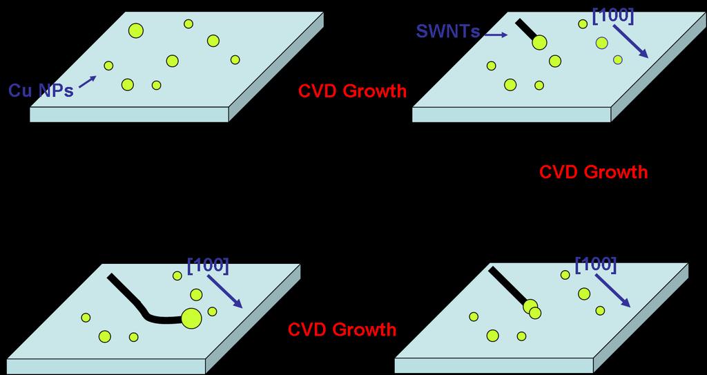
12 Mechanism


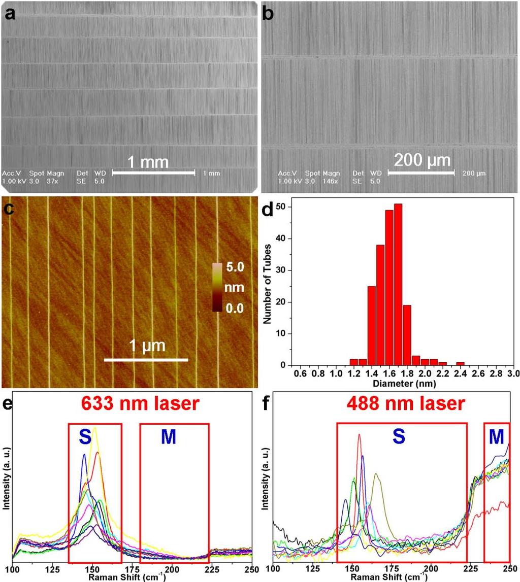
13 Cu catalytic growth of CNTs with EtOH as carbon source a b 1 mm 500 µm c d 5.0 nm µm 200 nm
14 Semiconducting Aligned CNTs
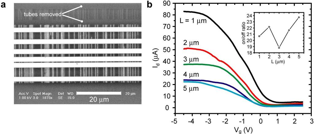
15 Semiconducting Aligned CNTs

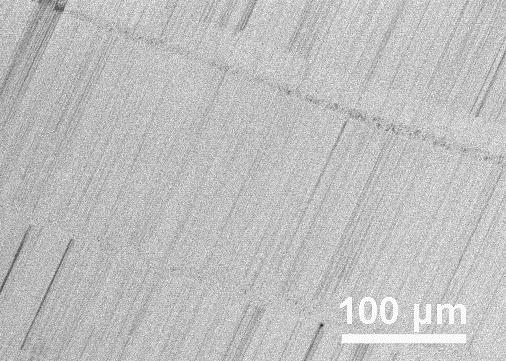
16 CNTs Grown on SiO2 Under Same Conditions do not Show Selectivity

17 Aligned CNTs on Quartz Under different Conditions also not Showing Selectivity
18 What is the Next Step? Increase the Current Density of Devices for High frequency devices; Density Increase; Diameter Control; Understanding.


19 SWNT Density Improvement and Current Enhancement Two-step CVD 0.05V bias Density and output current: 1.5~2 times increase John Rogers and et al. Adv. Mater. 2010, 22,


20 Low-pressure CVD and stacked multiple transfer Chongwu Zhou and et al. Nano Research ASAP 1V bias First growth: 15 tubes/μm; After four layer transfer: 55 tubes/μm; Highest on-sate current density of 92.4 μa/μm

21 How to further increase current density? Strategy I: Synthesis of SWNTs with large diameter Phaedon Avouris and et al. Nano Lett 2005, 5, 1497 Yu-Chih Tseng and et al. Nano Lett 2006, 6, 1364 Ideal contact can be formed between Pd and SWNTs with the diameter above 1.4 nm. Large diameter SWNT (>1.4 nm) can carry two orders of magnitude higher current than small diameter SWNTs (<1.0 nm).


22 Methane CVD 1.1± 0.4 nm Our ethanol CVD 1.2 ± 0.3 nm LP ethanol CVD ± nm Peter Burke and et al. Nano Res2008,1,158 Our methanol/ethanol CVD Jie Liu and et al. J. Am. Chem. Soc. 2008, 130, Chongwu Zhou and et al. Nano Res. ASAP Density is not very high. 1.4~1.8 nm with an average diameter of ~1.65 nm Jie Liu and et al. Nano Lett. 2009, 9,


23 Strategy II: Increase the catalyzing efficiency of catalyst particles. First CVD Growth C 2 H 4, H 2 O, H 2 and Ar 800 o C ~ 850 o C Fe x O y nanoparticles C 2 H 5 OH, CH 3 OH, H 2 and Ar 900 o C Second CVD Growth Some catalyst particles still active after first CVD growth of CNT forests. Jie Liu and et al. J. Am. Chem. Soc. 2010, 132,


24 Experimental Design: Multiple-Cycle Growth 900 o C Aim: activate more catalyst particles and synthesize largediameter SWNTs.

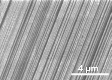
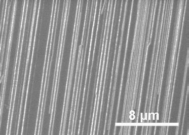
25 Experimental Results: Horizontally aligned array of SWNTs with highly dense packing Density is too high to count the number of SWNTs by SEM!


26 AFM Characterization The density of SWNT array is 20 ~ 40 SWNTs/μm, which is 3~4 times as high as the array density made by one-time growth. In some areas, SWNTs almost form a continual monolayer film. Even AFM is hard to distinguish the isolated SWNTs.

27 Raman Characterization RBM G band From quartz surface Raman spectra collected in the 16 spots. 633 nm laser.

 Total number : 120")


28 HRTEM Characterization (transfer SWNT array to copper grid by using PMMA film) Total number : 120 Diameter distribution: 2.38 ± 0.48 nm Maximum: 3.73 nm; Minimum: 1.18 nm Only 3 SWNTs with the diameter below 1.4nm.


29 Mechanism? ne-time Growth Two-cycle Growth Three-cycle Growth Four-cycle Growth 4~ 10 SWNT/μm 10~20 SWNT/μm 20~ 40 SWNT/μm 2~ 5 SWNT/μm


30 Hypothesis: Increase the Probability of SWNTs Nucleation At the stage of carbon feeding rate increase, different size catalyst particles start to nucleate SWNTs due to different carbon feeding rate. However, not every particle can nucleate SWNT at this stage, even for same size nanoparticles. There is a nucleation probability problem. Multiple-cycle growth can greatly increase the chances of SWNT nucleation on catalyst particles.

31 Proof: new nanotubes grow out from catalyst area. First CVD Growth Second CVD Growth At the same time, short tubes were observed after second CVD growth, which indicates some old nanotubes were etched in the second growth.

32 Etching Effect Study: Keep Methanol and Ar as the Protection Gas in the Off-steps In order to further investigate the etching effect, we used methanol and Ar as the protecting gas instead of pure Ar in the off steps between two CVD growth steps in a threecycle growth. As shown in SEM images, very few nanotubes were grown on quartz substrate. It means most of nanotubes were etched by methanol.
33 Current Thinking Density increase of SWNT array is due to the higher efficiency of nucleation. This hypothesis is confirmed by comparison of one-time, two-cycle and three-cycle and four-cycle growth results and in-situ analyzing SEM images of the same catalyst area on a quartz wafer after the first growth and after the second growth. The existence of etching effect during the CVD growth process has been discovered. In the fourth growth cycle, the etching effect starts to dominate over the growth, then resulting in the decrease of SWNT density. We speculate that it is from OH group because oxygen atom in OH group has a weak oxidation function and can react with amorphous carbon. This etching effect is likely the reason that only large-diameter SWNTs were obtained in multiplecycle CVD growth.
34 Acknowledgement Funding ONR NRL(N G902) Duke University People Dr. Lei Ding Dr. Weiwei Zhou Dr. Alex Tselev Dr. Dongning Yuan Professor Yan Li (Peiking University) and students
35
Selective Growth of Well-Aligned Semiconducting Single-Walled Carbon Nanotubes
 Letter Selective Growth of Well-Aligned Semiconducting Single-Walled Carbon Nanotubes Lei Ding, Alexander Tselev, Jinyong Wang, Dongning Yuan, Haibin Chu, Thomas P. McNicholas, Yan Li, and Jie Liu Nano
Orthogonal Orientation Control of Carbon Nanotube Growth
 Published on Web 12/14/2009 Orthogonal Orientation Control of Carbon Nanotube Growth Weiwei Zhou, Lei Ding, Sungwoo Yang, and Jie Liu* Department of Chemistry, Duke UniVersity, Durham, North Carolina 27708
Carbon Nanotubes for Interconnect Applications Franz Kreupl, Andrew P. Graham, Maik Liebau, Georg S. Duesberg, Robert Seidel, Eugen Unger
 Carbon Nanotubes for Interconnect Applications Franz Kreupl, Andrew P. Graham, Maik Liebau, Georg S. Duesberg, Robert Seidel, Eugen Unger Infineon Technologies Corporate Research Munich, Germany Outline
CNT-based photovoltaic and light emitting diodes
 Brazil-China Scientific Symposium: PKU & FAPESP, 214.6.16 CNT-based photovoltaic and light emitting diodes Lian-Mao Peng Department of Electronics Peking University Why Carbon Nanotube? Carbon nanotube
Manufacture of Nanostructures for Power Electronics Applications
 Manufacture of Nanostructures for Power Electronics Applications Brian Hunt and Jon Lai Etamota Corporation 2672 E. Walnut St. Pasadena, CA 91107 APEC, Palm Springs Feb. 23rd, 2010 1 Background Outline
Supplementary Figure S1. AFM images of GraNRs grown with standard growth process. Each of these pictures show GraNRs prepared independently,
 Supplementary Figure S1. AFM images of GraNRs grown with standard growth process. Each of these pictures show GraNRs prepared independently, suggesting that the results is reproducible. Supplementary Figure
Supporting Information
 Supporting Information Direct Chemical Vapor Deposition-Derived Graphene Glasses Targeting Wide Ranged Applications Jingyu Sun, Yubin Chen, Manish Kr. Priydarshi, Zhang Chen, Alicja Bachmatiuk,, Zhiyu
SUPPLEMENTARY INFORMATION
 SUPPLEMENTARY INFORMATION Phonon populations and electrical power dissipation in carbon nanotube transistors Supplemental Information Mathias Steiner 1, Marcus Freitag 1, Vasili Perebeinos 1, James C.
Xing Sheng, 微纳光电子材料与器件工艺原理. Doping 掺杂. Xing Sheng 盛兴. Department of Electronic Engineering Tsinghua University
 微纳光电子材料与器件工艺原理 Doping 掺杂 Xing Sheng 盛兴 Department of Electronic Engineering Tsinghua University xingsheng@tsinghua.edu.cn 1 Semiconductor PN Junctions Xing Sheng, EE@Tsinghua LEDs lasers detectors solar
Carbon-Based Electronics: Will there be a carbon age to follow the silicon age? Jeffrey Bokor EECS Department UC Berkeley
 Carbon-Based Electronics: Will there be a carbon age to follow the silicon age? Jeffrey Bokor EECS Department UC Berkeley jbokor@eecs.berkeley.edu Solid State Seminar 9-13-13 1 Outline Review of development
Recap (so far) Low-Dimensional & Boundary Effects
 Low-Dimensional & Boundary Effects") Recap (so far) Ohm s & Fourier s Laws Mobility & Thermal Conductivity Heat Capacity Wiedemann-Franz Relationship Size Effects and Breakdown of Classical Laws 1 Low-Dimensional & Boundary Effects Energy
Recap (so far) Ohm s & Fourier s Laws Mobility & Thermal Conductivity Heat Capacity Wiedemann-Franz Relationship Size Effects and Breakdown of Classical Laws 1 Low-Dimensional & Boundary Effects Energy
Supporting Information
 Supporting Information Repeated Growth Etching Regrowth for Large-Area Defect-Free Single-Crystal Graphene by Chemical Vapor Deposition Teng Ma, 1 Wencai Ren, 1 * Zhibo Liu, 1 Le Huang, 2 Lai-Peng Ma,
A new method of growing graphene on Cu by hydrogen etching
 A new method of growing graphene on Cu by hydrogen etching Linjie zhan version 6, 2015.05.12--2015.05.24 CVD graphene Hydrogen etching Anisotropic Copper-catalyzed Highly anisotropic hydrogen etching method
Large Scale Direct Synthesis of Graphene on Sapphire and Transfer-free Device Fabrication
 Supplementary Information Large Scale Direct Synthesis of Graphene on Sapphire and Transfer-free Device Fabrication Hyun Jae Song a, Minhyeok Son a, Chibeom Park a, Hyunseob Lim a, Mark P. Levendorf b,
Determining Carbon Nanotube Properties from Raman. Scattering Measurements
 Determining Carbon Nanotube Properties from Raman Scattering Measurements Ying Geng 1, David Fang 2, and Lei Sun 3 1 2 3 The Institute of Optics, Electrical and Computer Engineering, Laboratory for Laser
Carbon Nanotubes: Development of Nanomaterials for Hydrogen Storage
 Carbon Nanotubes: Development of Nanomaterials for Hydrogen Storage Hongjie Dai Department of Chemistry & Laboratory for Advanced Materials Stanford University GCEP, September 19, 2006 Outline Can carbon
Investigation on the growth of CNTs from SiO x and Fe 2 O 3 nanoparticles by in situ TEM
 The 5 th Workshop on Nucleation and Growth Mechanisms of SWCNTs Investigation on the growth of CNTs from SiO x and Fe 2 O 3 nanoparticles by in situ TEM Chang Liu Shenyang National Laboratory for Materials
Lattice-Oriented Growth of Single-Walled Carbon Nanotubes
 Letter Subscriber access provided by DUKE UNIV Lattice-Oriented Growth of Single-Walled Carbon Nanotubes Ming Su, Yan Li, Benjamin Maynor, Alper Buldum, Jian Ping Lu, and Jie Liu J. Phys. Chem. B, 2000,
Improving the Electrical Contact Property of Single-Walled Carbon Nanotube Arrays by Electrodeposition
 www.nmletters.org Improving the Electrical Contact Property of Single-Walled Carbon Nanotube Arrays by Electrodeposition Min Zhang (Received 10 August 2013; accepted 10 September 2013; published online
Multicolor Graphene Nanoribbon/Semiconductor Nanowire. Heterojunction Light-Emitting Diodes
 Multicolor Graphene Nanoribbon/Semiconductor Nanowire Heterojunction Light-Emitting Diodes Yu Ye, a Lin Gan, b Lun Dai, *a Hu Meng, a Feng Wei, a Yu Dai, a Zujin Shi, b Bin Yu, a Xuefeng Guo, b and Guogang
CVD growth of Graphene. SPE ACCE presentation Carter Kittrell James M. Tour group September 9 to 11, 2014
 CVD growth of Graphene SPE ACCE presentation Carter Kittrell James M. Tour group September 9 to 11, 2014 Graphene zigzag armchair History 1500: Pencil-Is it made of lead? 1789: Graphite 1987: The first
SUPPLEMENTARY INFORMATION. Observation of tunable electrical bandgap in large-area twisted bilayer graphene synthesized by chemical vapor deposition
 SUPPLEMENTARY INFORMATION Observation of tunable electrical bandgap in large-area twisted bilayer graphene synthesized by chemical vapor deposition Jing-Bo Liu 1 *, Ping-Jian Li 1 *, Yuan-Fu Chen 1, Ze-Gao
GHZ ELECTRICAL PROPERTIES OF CARBON NANOTUBES ON SILICON DIOXIDE MICRO BRIDGES
 GHZ ELECTRICAL PROPERTIES OF CARBON NANOTUBES ON SILICON DIOXIDE MICRO BRIDGES SHENG F. YEN 1, HAROON LAIS 1, ZHEN YU 1, SHENGDONG LI 1, WILLIAM C. TANG 1,2, AND PETER J. BURKE 1,2 1 Electrical Engineering
Supplementary Figure 1 Experimental setup for crystal growth. Schematic drawing of the experimental setup for C 8 -BTBT crystal growth.
 Supplementary Figure 1 Experimental setup for crystal growth. Schematic drawing of the experimental setup for C 8 -BTBT crystal growth. Supplementary Figure 2 AFM study of the C 8 -BTBT crystal growth
铁硒超导薄膜的原位制 备和电子结构测量 谢斌平 复旦大学 杭州 2014 全国表面分析应用技术学术交流会及赛默飞世尔科技 XPS 应用及设备维护技术培训班
 铁硒超导薄膜的原位制 备和电子结构测量 谢斌平 复旦大学 2014.04.24 杭州 2014 全国表面分析应用技术学术交流会及赛默飞世尔科技 XPS 应用及设备维护技术培训班 Outline 1. Experimental setup----ombe+mbe+arpes 2. Heterostructure Design and in-situ ARPES study FeSe/STO films
SUPPLEMENTARY INFORMATION
 SUPPLEMENTARY INFORMATION Facile Synthesis of High Quality Graphene Nanoribbons Liying Jiao, Xinran Wang, Georgi Diankov, Hailiang Wang & Hongjie Dai* Supplementary Information 1. Photograph of graphene
Hydrogenation of Single Walled Carbon Nanotubes
 Hydrogenation of Single Walled Carbon Nanotubes Anders Nilsson Stanford Synchrotron Radiation Laboratory (SSRL) and Stockholm University Coworkers and Ackowledgement A. Nikitin 1), H. Ogasawara 1), D.
Supplementary Figure 1 Dark-field optical images of as prepared PMMA-assisted transferred CVD graphene films on silicon substrates (a) and the one
 and the one") Supplementary Figure 1 Dark-field optical images of as prepared PMMA-assisted transferred CVD graphene films on silicon substrates (a) and the one after PBASE monolayer growth (b). 1 Supplementary Figure
Supplementary Figure 1 Dark-field optical images of as prepared PMMA-assisted transferred CVD graphene films on silicon substrates (a) and the one after PBASE monolayer growth (b). 1 Supplementary Figure
CARBON NANOTUBE ARRAYS
 CARBON NANOTUBE ARRAYS This colorized, perspective SEM image shows aligned arrays of single-walled carbon nanotubes grown on a quartz substrate in two sequential cycles of chemical vapor deposition (red
Introduction to Nanotechnology Chapter 5 Carbon Nanostructures Lecture 1
 Introduction to Nanotechnology Chapter 5 Carbon Nanostructures Lecture 1 ChiiDong Chen Institute of Physics, Academia Sinica chiidong@phys.sinica.edu.tw 02 27896766 Section 5.2.1 Nature of the Carbon Bond
Supplementary Figures Supplementary Figure 1
 Supplementary Figures Supplementary Figure 1 Optical images of graphene grains on Cu after Cu oxidation treatment at 200 for 1m 30s. Each sample was synthesized with different H 2 annealing time for (a)
Supporting information:
 Epitaxially Integrating Ferromagnetic Fe 1.3 Ge Nanowire Arrays on Few-Layer Graphene Hana Yoon, Taejoon Kang, Jung Min Lee, Si-in Kim, Kwanyong Seo, Jaemyung Kim, Won Il Park, and Bongsoo Kim,* Department
Role of Catalysts in the Surface Synthesis of Single-Walled Carbon Nanotubes
 Nano Res (2009) 2: 593 598 DOI 10.1007/s12274-009-9068-x Review Article 00593 Role of Catalysts in the Surface Synthesis of Single-Walled Carbon Nanotubes Weiwei Zhou, Lei Ding, and Jie Liu Department
Selective Preparation of Semiconducting Single-Walled Carbon Nanotubes: From Fundamentals to Applications By Jinghua Li
 Selective Preparation of Semiconducting Single-Walled Carbon Nanotubes: From Fundamentals to Applications By Jinghua Li Department of Chemistry Duke University Approved: Jie Liu, Supervisor Desiree Plata
Large-area growth of ultra-high-density single-walled carbon nanotube arrays on sapphire surface
 Nano Research 2015, 8(11): 3694 3703 DOI 10.1007/s12274-015-0869-9 Large-area growth of ultra-high-density single-walled carbon nanotube arrays on sapphire surface Lixing Kang 1,2,3, Yue Hu 2, Hua Zhong
Yan Li *, Supporting Information
 Decoration of Gold Nanoparticles on Surface-Grown Single-Walled Carbon Nanotubes for Detection of Every Nanotube by Surface-Enhanced Raman Spectroscopy Haibin Chu,, Jinyong Wang, Lei Ding, Dongning Yuan,
There's Plenty of Room at the Bottom
 There's Plenty of Room at the Bottom 12/29/1959 Feynman asked why not put the entire Encyclopedia Britannica (24 volumes) on a pin head (requires atomic scale recording). He proposed to use electron microscope
Supporting Information for
 Supporting Information for Multilayer CuO@NiO Hollow Spheres: Microwave-Assisted Metal-Organic-Framework Derivation and Highly Reversible Structure-Matched Stepwise Lithium Storage Wenxiang Guo, Weiwei
Selective Synthesis of Large Diameter, Highly Conductive and. High Density Single-Walled Carbon Nanotubes by Thiophene-
 Page 1 of 19 Selective Synthesis of Large Diameter, Highly Conductive and High Density Single-Walled Carbon Nanotubes by Thiophene- Assisted Chemical Vapor Deposition Method on Transparent Substrates Jinghua
1-amino-9-octadecene, HAuCl 4, hexane, ethanol 55 o C, 16h AuSSs on GO
 Supplementary Figures GO Supplementary Figure S1 1-amino-9-octadecene, HAuCl 4, hexane, ethanol 55 o C, 16h AuSSs on GO Schematic illustration of synthesis of Au square sheets on graphene oxide sheets.
Control of Diameter Distribution of Single-walled Carbon Nanotubes Using the Zeolite-CCVD Method
 22 Special Issue Nano-structure Controls of Functional Powders Research Report Control of Diameter Distribution of Single-walled Carbon Nanotubes Using the Zeolite-CCVD Method Atsuto Okamoto, Hisanori
Understanding Irreducible and Reducible Oxides as Catalysts for Carbon Nanotubes and Graphene Formation
 Wright State University CORE Scholar Special Session 5: Carbon and Oxide Based Nanostructured Materials (2011) Special Session 5 6-2011 Understanding Irreducible and Reducible Oxides as Catalysts for Carbon
Chapter 7. Carbon Nanotubes. 1. Introduction of CNTs 2. Application of CNTs 3. Growth of CNTs 4. Critical Issues in CNT growth
 Chapter 7. Carbon Nanotubes 1. Introduction of CNTs 2. Application of CNTs 3. Growth of CNTs 4. Critical Issues in CNT growth 2018 년 4 월 12 일. 우주엘리베이터가첫운행을시작한다!! 1996 년노벨화학상 크로토 (Kroto), 스몰리 (Smalley),
Supported Ni catalysts from nominal monolayer grow single-walled carbon nanotubes.
 Supported Ni catalysts from nominal monolayer grow single-walled carbon nanotubes. Kazunori Kakehi a, Suguru Noda a, *, Shohei Chiashi b, Shigeo Maruyama b a Department of Chemical System Engineering,
Doping-Free Fabrication of Carbon Nanotube Based Ballistic CMOS Devices and Circuits
 Doping-Free Fabrication of Carbon Nanotube Based Ballistic CMOS Devices and Circuits NANO LETTERS 2007 Vol. 7, No. 12 3603-3607 Zhiyong Zhang, Xuelei Liang,*, Sheng Wang, Kun Yao, Youfan Hu, Yuzhen Zhu,
A. Optimizing the growth conditions of large-scale graphene films
 1 A. Optimizing the growth conditions of large-scale graphene films Figure S1. Optical microscope images of graphene films transferred on 300 nm SiO 2 /Si substrates. a, Images of the graphene films grown
Nanostrukturphysik (Nanostructure Physics)
") Nanostrukturphysik (Nanostructure Physics) Prof. Yong Lei & Dr. Yang Xu Fachgebiet 3D-Nanostrukturierung, Institut für Physik Contact: yong.lei@tu-ilmenau.de; yang.xu@tu-ilmenau.de Office: Unterpoerlitzer
Nanostrukturphysik (Nanostructure Physics) Prof. Yong Lei & Dr. Yang Xu Fachgebiet 3D-Nanostrukturierung, Institut für Physik Contact: yong.lei@tu-ilmenau.de; yang.xu@tu-ilmenau.de Office: Unterpoerlitzer
Supplementary Figure S1. AFM characterizations and topographical defects of h- BN films on silica substrates. (a) (c) show the AFM height
 (c) show the AFM height") Supplementary Figure S1. AFM characterizations and topographical defects of h- BN films on silica substrates. (a) (c) show the AFM height topographies of h-bn film in a size of ~1.5µm 1.5µm, 30µm 30µm
Supplementary Figure S1. AFM characterizations and topographical defects of h- BN films on silica substrates. (a) (c) show the AFM height topographies of h-bn film in a size of ~1.5µm 1.5µm, 30µm 30µm
SYNTHESIS OF CARBON NANOTUBES BY CATALYTIC CVD USING Fe-Mo/MgO AND Fe- Mo/Al 2 O 3 CATALYSTS. Abstract. Introduction. Experimental
 SYNTHESIS OF CARBON NANOTUBES BY CATALYTIC CVD USING Fe-Mo/MgO AND Fe- Mo/Al 2 O 3 CATALYSTS Shinn-Shyong Tzeng, Ting-Bin Liang, Sheng-Chuan Wang, Ting-Yu Wu and Yu-Hun Lin Department of Materials Engineering,
Efficient and controlled synthesis of SWCNTs by enhanced direct injection pyrolytic synthesis (edips) method and their applications
 method and their applications") Efficient and controlled synthesis of SWCNTs by enhanced direct injection pyrolytic synthesis (edips) method and their applications Guadalupe Workshop 2011 April 8 th -12 th, 2011 Texas USA Takeshi Saito
Efficient and controlled synthesis of SWCNTs by enhanced direct injection pyrolytic synthesis (edips) method and their applications Guadalupe Workshop 2011 April 8 th -12 th, 2011 Texas USA Takeshi Saito
Carbon Nanotube Electronics
 Carbon Nanotube Electronics Jeorg Appenzeller, Phaedon Avouris, Vincent Derycke, Stefan Heinz, Richard Martel, Marko Radosavljevic, Jerry Tersoff, Shalom Wind H.-S. Philip Wong hspwong@us.ibm.com IBM T.J.
Diameter-Controlled Growth of Carbon Nanotubes
 106 Chapter 6: Microdischarge Synthesis of Fe Nanoparticles for Diameter-Controlled Growth of Carbon Nanotubes 6.1. Introduction Nanometer-sized materials represent the future building blocks of nanoscale
Supporting Information. Direct n- to p-type Channel Conversion in Monolayer/Few-Layer WS 2 Field-Effect Transistors by Atomic Nitrogen Treatment
 Supporting Information Direct n- to p-type Channel Conversion in Monolayer/Few-Layer WS 2 Field-Effect Transistors by Atomic Nitrogen Treatment Baoshan Tang 1,2,, Zhi Gen Yu 3,, Li Huang 4, Jianwei Chai
Submonolayer collections of single-walled carbon nanotubes
 Scaling Properties in Transistors That Use Aligned Arrays of Single-Walled Carbon Nanotubes pubs.acs.org/nanolett Xinning Ho, Lina Ye, Slava V. Rotkin, Qing Cao, Sakulsuk Unarunotai, Shuaib Salamat, Muhammad
Micro Chemical Vapor Deposition System: Design and Verification
 Micro Chemical Vapor Deposition System: Design and Verification Q. Zhou and L. Lin Berkeley Sensor and Actuator Center, Department of Mechanical Engineering, University of California, Berkeley 2009 IEEE
Aligned Arrays of Single-Walled Carbon Nanotubes Generated from Random Networks by Orientationally Selective Laser Ablation
 Aligned Arrays of Single-Walled Carbon Nanotubes Generated from Random Networks by Orientationally Selective Laser Ablation NANO LETTERS 2004 Vol. 4, No. 12 2421-2426 Coskun Kocabas,, Matthew A. Meitl,,
Layer-modulated synthesis of uniform tungsten disulfide nanosheet using gas-phase precursors.
 Layer-modulated synthesis of uniform tungsten disulfide nanosheet using gas-phase precursors. Jusang Park * Hyungjun Kim School of Electrical and Electronics Engineering, Yonsei University, 262 Seongsanno,
Electric-field-directed growth of carbon nanotubes in two dimensions
 Electric-field-directed growth of carbon nanotubes in two dimensions Alireza Nojeh a),b) Department of Electrical Engineering, Stanford University, Stanford, California 94305 Ant Ural b),c) Department
Supporting Information
 Electronic Supplementary Material (ESI) for ChemComm. This journal is The Royal Society of Chemistry 2014 Supporting Information Controllable Atmospheric Pressure Growth of Mono-layer, Bi-layer and Tri-layer
The goal of this project is to enhance the power density and lowtemperature efficiency of solid oxide fuel cells (SOFC) manufactured by atomic layer
 manufactured by atomic layer") Stanford University Michael Shandalov1, Shriram Ramanathan2, Changhyun Ko2 and Paul McIntyre1 1Department of Materials Science and Engineering, Stanford University 2Division of Engineering and Applied
Stanford University Michael Shandalov1, Shriram Ramanathan2, Changhyun Ko2 and Paul McIntyre1 1Department of Materials Science and Engineering, Stanford University 2Division of Engineering and Applied
Electrochemically Synthesized Multi-block
 Electrochemically Synthesized Multi-block Nanorods Sungho Park SungKyunKwan University, Department of Chemistry & SKKU Advanced Institute of Nanotechnology (SAINT) J. Am. Chem. Soc. 2003, 125, 2282-2290
Optical Spectroscopy of Single-Walled Carbon Nanotubes
 Optical Spectroscopy of Single-Walled Carbon Nanotubes Louis Brus Chemistry Department, Columbia University Groups: Heinz, O Brien, Hone, Turro, Friesner, Brus 1. SWNT Luminescence dynamics psec pump-probe
File name: Supplementary Information Description: Supplementary Figures, Supplementary Notes, Supplementary Tables, Supplementary References
 File name: Supplementary Information Description: Supplementary Figures, Supplementary Notes, Supplementary Tables, Supplementary References Supplementary Figure 1 Illustration of the reaction chamber
Carbon Nanotubes in Interconnect Applications
 Carbon Nanotubes in Interconnect Applications Page 1 What are Carbon Nanotubes? What are they good for? Why are we interested in them? - Interconnects of the future? Comparison of electrical properties
ALIGNED CARBON NANOTUBES FOR MULTIFUNCTIONAL NANOCOMPOSITES AND NANODEVICES:
 ALIGNED CARBON NANOTUBES FOR MULTIFUNCTIONAL NANOCOMPOSITES AND NANODEVICES: Multicomponent Micropatterned Aligned Carbon Nanotube Devices with Reversibly Switchable Electronic Properties for Multifunctional
Growth window and possible mechanism of millimeter-thick single-walled carbon nanotube forests
 Growth window and possible mechanism of millimeter-thick single-walled carbon nanotube forests Kei Hasegawa 1, Suguru Noda 1,*, Hisashi Sugime 1, Kazunori Kakehi 1, Shigeo Maruyama 2 and Yukio Yamaguchi
SUPPLEMENTARY INFORMATION
 SUPPLEMENTARY INFORMATION Linking catalyst composition to chirality distributions of as-grown singlewalled carbon nanotubes by tuning Ni x Fe 1-x nanoparticles Supplementary Information Wei-Hung Chiang
Measuring charge transport through molecules
 Measuring charge transport through molecules utline Indirect methods 1. ptical techniques 2. Electrochemical techniques Direct methods 1. Scanning probe techniques 2. In-plane electrodes 3. Break junctions
Transport Properties of Novel Carbon Nanotubes and Nanopeapods
 Transport Properties of Novel Carbon Nanotubes and Nanopeapods Takashi Shimada, Yutaka Ohno, Toshiya Okazaki, Toshiki Sugai, Yousuke Nosho, Kazutomo Suenaga, Shigeru Kishimoto, Takashi Mizutani, and Hisanori
crystals were phase-pure as determined by x-ray diffraction. Atomically thin MoS 2 flakes were
 Nano Letters (214) Supplementary Information for High Mobility WSe 2 p- and n-type Field Effect Transistors Contacted by Highly Doped Graphene for Low-Resistance Contacts Hsun-Jen Chuang, Xuebin Tan, Nirmal
Materials Chemistry C
 Journal of Materials Chemistry C Accepted Manuscript This is an Accepted Manuscript, which has been through the Royal Society of Chemistry peer review process and has been accepted for publication. Accepted
Research Opportunities in Macroelectronics. Motivation, Application Overview. Materials Classes, Challenges. Patterning Techniques, Challenges
 Research Opportunities in Macroelectronics Motivation, Application Overview Materials Classes, Challenges Patterning Techniques, Challenges John A. Rogers -- University of Illinois at Urbana/Champaign
Supplementary Figure 1. (a-b) EDX of Mo 2 and Mo 2
 EDX of Mo 2 and Mo 2") Supplementary Figure 1. (a-b) EDX of Mo 2 C@NPC/NPRGO and Mo 2 C@NPC. Supplementary Figure 2. (a) SEM image of PMo 12 2-PPy, (b) TEM, (c) HRTEM, (d) STEM image and EDX elemental mapping of C, N, P, and
Supplementary Figure 1. (a-b) EDX of Mo 2 C@NPC/NPRGO and Mo 2 C@NPC. Supplementary Figure 2. (a) SEM image of PMo 12 2-PPy, (b) TEM, (c) HRTEM, (d) STEM image and EDX elemental mapping of C, N, P, and
performance electrocatalytic or electrochemical devices. Nanocrystals grown on graphene could have
 Nanocrystal Growth on Graphene with Various Degrees of Oxidation Hailiang Wang, Joshua Tucker Robinson, Georgi Diankov, and Hongjie Dai * Department of Chemistry and Laboratory for Advanced Materials,
LETTERS. Sangjin Han, Taekyung Yu, Jongnam Park, Bonil Koo, Jin Joo, and Taeghwan Hyeon* Seunghun Hong and Jiwoon Im
 Copyright 2004 by the American Chemical Society VOLUME 108, NUMBER 24, JUNE 17, 2004 LETTERS Diameter-Controlled Synthesis of Discrete and Uniform-Sized Single-Walled Carbon Nanotubes Using Monodisperse
NANO LETTERS Vol. 7, No C. Kocabas,, N. Pimparkar,, O. Yesilyurt, S. J. Kang, M. A. Alam,*, and J. A.
 Experimental and Theoretical Studies of Transport through Large Scale, Partially Aligned Arrays of Single-Walled Carbon Nanotubes in Thin Film Type Transistors NANO LETTERS 2007 Vol. 7, No. 5 1195-1202
Electrical Contacts to Carbon Nanotubes Down to 1nm in Diameter
 1 Electrical Contacts to Carbon Nanotubes Down to 1nm in Diameter Woong Kim, Ali Javey, Ryan Tu, Jien Cao, Qian Wang, and Hongjie Dai* Department of Chemistry and Laboratory for Advanced Materials, Stanford
Supplementary Information
 Supplementary Information Supplementary Figure 1. fabrication. A schematic of the experimental setup used for graphene Supplementary Figure 2. Emission spectrum of the plasma: Negative peaks indicate an
Two-Dimensional (C 4 H 9 NH 3 ) 2 PbBr 4 Perovskite Crystals for. High-Performance Photodetector. Supporting Information for
 2 PbBr 4 Perovskite Crystals for. High-Performance Photodetector. Supporting Information for") Supporting Information for Two-Dimensional (C 4 H 9 NH 3 ) 2 PbBr 4 Perovskite Crystals for High-Performance Photodetector Zhenjun Tan,,ǁ, Yue Wu,ǁ, Hao Hong, Jianbo Yin, Jincan Zhang,, Li Lin, Mingzhan
Supporting Information for Two-Dimensional (C 4 H 9 NH 3 ) 2 PbBr 4 Perovskite Crystals for High-Performance Photodetector Zhenjun Tan,,ǁ, Yue Wu,ǁ, Hao Hong, Jianbo Yin, Jincan Zhang,, Li Lin, Mingzhan
Supplementary Materials for
 advances.sciencemag.org/cgi/content/full/2/7/e1600322/dc1 Supplementary Materials for Ultrasensitive molecular sensor using N-doped graphene through enhanced Raman scattering Simin Feng, Maria Cristina
Saturable absorbers incorporating carbon nanotubes directly synthesized onto substrates/fibers and their application to mode-locked fiber lasers
 Saturable absorbers incorporating carbon nanotubes directly synthesized onto substrates/fibers and their application to mode-locked fiber lasers S. Yamashita (1), S. Maruyama (2), Y. Murakami (2), Y. Inoue
Controlled continuous spinning of fibres of single wall carbon nanotubes
 Controlled continuous spinning of fibres of single wall carbon nanotubes Guadalupe Workshop 8-12 April 2011 Krzysztof Koziol and Alan Windle kk292@cam.ac.uk Department of Materials Science and Metallurgy
The outstanding potential of using
 Selective Synthesis and Device Applications of Semiconducting Single-Walled Carbon Nanotubes Using Isopropyl Alcohol as Feedstock Yuchi Che,, Chuan Wang,, Jia Liu,, Bilu Liu, Xue Lin, Jason Parker, Cara
SUPPLEMENTARY INFORMATION
 doi:10.1038/nature21051 1. Methods and synthesis 1.1 Synthesis of mono-dispersed catalyst precursors on sapphire Typically, 0.088g (NH 4 ) 6 Mo 7 O 24 4H 2 O was dissolved into 100 ml deionized water under
Supporting Information
 Supporting Information Monolithically Integrated Flexible Black Phosphorus Complementary Inverter Circuits Yuanda Liu, and Kah-Wee Ang* Department of Electrical and Computer Engineering National University
Supporting Information. Electronic Modulation of Electrocatalytically Active. Highly Efficient Oxygen Evolution Reaction
 Supporting Information Electronic Modulation of Electrocatalytically Active Center of Cu 7 S 4 Nanodisks by Cobalt-Doping for Highly Efficient Oxygen Evolution Reaction Qun Li, Xianfu Wang*, Kai Tang,
Evolution of graphene growth on Cu and Ni studied by carbon isotope
 Evolution of graphene growth on Cu and Ni studied by carbon isotope labeling Xuesong Li a, Weiwei Cai a, Luigi Colombo b*, and Rodney S. Ruoff a* Large-area graphene is a new material with properties that
Large-Area and Uniform Surface-Enhanced Raman. Saturation
 Supporting Information Large-Area and Uniform Surface-Enhanced Raman Spectroscopy Substrate Optimized by Enhancement Saturation Daejong Yang 1, Hyunjun Cho 2, Sukmo Koo 1, Sagar R. Vaidyanathan 2, Kelly
Design and Fabrication of Microheaters for Localized Carbon Nanotube Growth
 Design and Fabrication of Microheaters for Localized Carbon Nanotube Growth Y. Zhou 1, J. Johnson 1, L. Wu 1, S. Maley 2, A. Ural 1, and H. Xie 1 1 Department of Electrical and Computer Engineering, University
29: Nanotechnology. What is Nanotechnology? Properties Control and Understanding. Nanomaterials
 29: Nanotechnology What is Nanotechnology? Properties Control and Understanding Nanomaterials Making nanomaterials Seeing at the nanoscale Quantum Dots Carbon Nanotubes Biology at the Nanoscale Some Applications
4. Synthesis of graphene from methane, acetonitrile, xylene and
 CHAPTER 4 4. Synthesis of graphene from methane, acetonitrile, xylene and ethanol 4.1 Introduction In this chapter, the synthesis of graphene from three different carbon precursors include gases (methane,
Controlling the Interface-Areas of. Heterojunction Nanowires for High Performance Diodes
 Supporting Information Controlling the Interface-Areas of Organic/Inorganic Semiconductors Heterojunction Nanowires for High Performance Diodes Zheng Xue,, Hui Yang, Juan Gao, Jiaofu Li, Yanhuan Chen,
Supporting Information. Engineering Two-Dimensional Mass-Transport Channels
 Supporting Information Engineering Two-Dimensional Mass-Transport Channels of MoS 2 Nanocatalyst towards Improved Hydrogen Evolution Performance Ge Wang a, Jingying Tao a, Yijie Zhang a, Shengping Wang
Supplementary Information
 Supplementary Information Plasma-assisted reduction of graphene oxide at low temperature and atmospheric pressure for flexible conductor applications Seung Whan Lee 1, Cecilia Mattevi 2, Manish Chhowalla
Thermal Transport in Graphene and other Two-Dimensional Systems. Li Shi. Department of Mechanical Engineering & Texas Materials Institute
 Thermal Transport in Graphene and other Two-Dimensional Systems Li Shi Department of Mechanical Engineering & Texas Materials Institute Outline Thermal Transport Theories and Simulations of Graphene Raman
Use of Multi-Walled Carbon Nanotubes for UV radiation detection
 Use of Multi-Walled Carbon Nanotubes for UV radiation detection Viviana Carillo 11th Topical Seminar on Innovative Particle and Radiation Detectors (IPRD08) 1-4 October 2008 Siena, Italy A new nanostructured
SUPPLEMENTARY INFORMATION
 doi:.38/nature09979 I. Graphene material growth and transistor fabrication Top-gated graphene RF transistors were fabricated based on chemical vapor deposition (CVD) grown graphene on copper (Cu). Cu foil
Germanium nanowires: from synthesis, surface chemistry, assembly to devices
 1 Germanium nanowires: from synthesis, surface chemistry, assembly to devices Dunwei Wang Department of Chemistry, Stanford University In order to continue the ever impressive and successful scaling pace
Three-dimensional flexible and conductive interconnected graphene networks grown by chemical vapour deposition
 SUPPLEMENTARY INFORMATION Three-dimensional flexible and conductive interconnected graphene networks grown by chemical vapour deposition S1. Characterization of the graphene foam (GF) and GF/PDMS composites
Carbon nanotube arrays on silicon substrates and their possible application
 Physica E 8 (2000) 179 183 www.elsevier.nl/locate/physe Carbon nanotube arrays on silicon substrates and their possible application Shoushan Fan a;, Wenjie Liang a, Haiyan Dang a, Nathan Franklin b, Thomas