Transmission Electron Microscopy. Part #1 Diffraction Conventional Imaging
|
|
|
- Elisabeth Higgins
- 5 years ago
- Views:
Transcription


1 Transmission Electron Microscopy Part #1 Diffraction Conventional Imaging Nicolas Menguy Institut de Minéralogie, de Physique des Matériaux et de Cosmochimie Outline Part 1 : Conventional TEM - Transmission Electron Microscope - TEM sample - conventional imaging : bright field / dark field - electron diffraction Part 2 : Advanced TEM - high resolution imaging - STEM HAADF imaging - XEDS spectroscopy - EELS spectroscopy - advanced aberration-corrected TEM/STEM
2 Part 1 : Conventional TEM Introduction Transmission Electron Microscope - gun, lens TEM sample - specificity - preparation, - Focused Ion Beam (FIB) conventional imaging in TEM - image formation - origin of contrast - bright field, dark field electron diffraction - principle - applications Part 1 : Conventional TEM Introduction Transmission Electron Microscope - gun, lens TEM sample - specificity - preparation, - Focused Ion Beam (FIB) conventional imaging in TEM - image formation - origin of contrast - bright field, dark field electron diffraction - principle - applications


 for relativistic electron (U > 100 kev): λ = 2.")
3 Introduction how to see atomic structure of condensed matter? to see an object with a size d you need a wavelength λ such as : λ < d example : visible light 0.5 µm in general, to get information about the atomic structure, you need a wavelength λ 0.1 nm Electromagnetic radiation with λ 0.1 nm : X-rays problem : best x-ray microscope 10 nm X-ray diffraction (not a direct image) Introduction how to see atomic structure of condensed matter? Electron radiation de Broglie s relation (1924) for relativistic electron (U > 100 kev): λ = 2.51 pm for U = 200 kv electron beams can be focused electrostatic lenses magnetic lenses first transmission electron microscope build in 1931 Ernst Ruska (1986 Nobel Prize) E. Ruska et M. Knoll 1931
 identification/quantification of secondary/scattered radiations Introduction Elastic electron - matter interaction Low angle")
4 Introduction general principle of material analysis Incident beam (probe) secondary, scattered beams transmitted, scattered beams Required : knowledge of the incident beam (nature, intensity) knowledge of the radiation / matter interaction (at the quantum level) identification/quantification of secondary/scattered radiations Introduction Elastic electron - matter interaction Low angle diffusion : θ < kev Coulomb interaction with the electron cloud High angle diffusion / back scattering : θ > kev Coulomb interaction with the atom nucleus (Rutherford diffusion) Elastic interaction : no energy transfer the atom is not ionized

 conventional imaging in TEM - image formation - origin of contrast - bright field, dark field electron diffraction - principle")
5 Introduction Inelastic electron - matter interaction Atom ionization : The incident electron ejects a bound electron and then changes direction with an energy loss Brehmstrahlung : Incident electron can loss energy by Coulomb interaction with atom nucleus + phonons, plasmons, Inelastic interaction : energy transfer: the incident electron losses energy atom may be ionized Part 1 : Conventional TEM Introduction Transmission Electron Microscope - gun, lens TEM sample - specificity - preparation, - Focused Ion Beam (FIB) conventional imaging in TEM - image formation - origin of contrast - bright field, dark field electron diffraction - principle - applications


6 TEM gun X-ray detector column sample holder CCD camera/ EELS spectrometer TEM through the ages


!")

![10 5% 10 6% <%10 8% 10 9% Brightness%%[A%cm 2 %sr 1 ]% 10 4 %](/docs-images/86/93850446/images/7-5.jpg "%10 5% 3%10 5% 10 8% 10 9% CrossDover%diameter%[μm]% 20% %50%")
7 TEM gun 200 kv sample holder goniometer projector lenses condenser lenses objective lens view chamber film chamber + several detectors: - CCD camera - X-rays detector - EELS spectrometer - HAADF detector - Electron sources , 2015 W filament LaB 6 tip Schottky emitter (FEG) cold field emitter (CFEG)!! W! LaB6! W'ZrO!(FEG)! W!(CFEG)! Work%temperature%[K]% 2800% 2000% 1800% 300% Work%pressure%[Pa]% 10 5% 10 6% <%10 8% 10 9% Brightness%%[A%cm 2 %sr 1 ]% 10 4 % %10 5% 3%10 5% 10 8% 10 9% CrossDover%diameter%[μm]% 20% %50% 10% %20% 0.015% 0.01% % Energy%spread%[eV]% 1% %2% 0.5% %2% 0.6% 0.2% %0.4% analytical at the atomic scale


8 Electromagnetic lenses Rotational symmetric electromagnetic fields $ B Lorentz force Lorentz force acts on electrons as an optical lens acts on light focusing F=q v B Defects of electromagnetic lenses Chromatic aberration Chromatic aberration E E- E α ds = cc E α E ds
9 Defects of electromagnetic lenses Spherical aberration (1) Spherical aberration ds plan Gaussian de l image gaussienne image plane α plan de moindre confusion disk of least confusion d s = 1 2 c s α 3 The focus depends on the axial distance of the electron path Defects of electromagnetic lenses Spherical aberration (2) the image of a point is not a point a phase shift appears between diffracted beams! ideal lens real lens lowering the resolution ( 1.5 Å) $ images may be difficult to interpret


10 Defects of electromagnetic lenses diffraction Diffraction May appear, due to the contrast aperture α d d = 1.22 λ α Condenser system Three main components : C1 condenser C2 condenser condenser aperture To control: spot size beam intensity beam convergence
11 TEM optics gun condenser lens sample objective lens projector / magnifying lens screen Objective lens A B PO OBJ PO OBJ objective lens PF OBJ PF OBJ B A PI OBJ PI OBJ an image is formed in the "image" plane a diffraction pattern is visible in the back focal plane reciprocal space


 thickness < 100 nm mandatory 20 nm : ideal Nanoparticles")
12 Part 1 : Conventional TEM Introduction Transmission Electron Microscope - gun, lens TEM sample - specificity - preparation, - Focused Ion Beam (FIB) conventional imaging in TEM - image formation - origin of contrast - bright field, dark field electron diffraction - principle - applications TEM sample must be "transparent" to high energy electrons ( kev) thickness < 100 nm mandatory 20 nm : ideal Nanoparticles Particles Thin foils FIB


13 TEM sample preparation nanoparticles Homogeneous solid sample Homogeneous powder sample + ethanol Preliminary glow discharge exposition of the carbon grid may help particles spread TEM sample preparation thin foil Bulk sample 1 mm Mechanical polishing 30 µm ion polishing Ar+


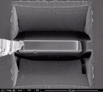


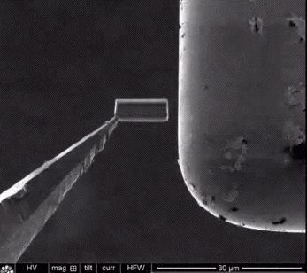
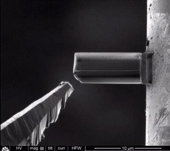

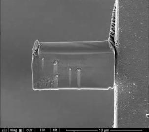
14 Thin foil preparation Focused Ion Beam ex situ lift out Pt protective layer Parallel trenches are made around the region of interest using ionic abrasion Foil thinning 50 nm Thin foil: 15 µm x 5 µm x 50 nm Thin foil is cut micromanipulator Transfer of the thin foil onto a TEM grid Thin foil preparation Focused Ion Beam in situ lift out


 conventional imaging in")

15 TEM sample holder Simple tilt double tilt cooling sample holder liquid N 2 liquid He in situ liquid/gaseous cell Part 1 : Conventional TEM Introduction Transmission Electron Microscope - gun, lens TEM sample - specificity - preparation, - Focused Ion Beam (FIB) conventional imaging in TEM - image formation - origin of contrast - bright field, dark field electron diffraction - principle - applications
 simultaneously an image or a diffraction pattern of your sample : 10 nm Magnetite Fe 3 O 4 <110> zone")
16 Electron Matter interactions thin sample electron incident beam backscattered e X-ray photons XEDS Visible light secondary, Auger e absorbed e inelastically scattered e EELS transmitted e elastically scattered e diffraction, imaging, HREM IMAGE and DIFFRACTION modes With TEM, you can get (almost) simultaneously an image or a diffraction pattern of your sample : 10 nm Magnetite Fe 3 O 4 <110> zone axis diffraction pattern

 IP OBJ image plane F.T.(F.T.(Ψ i ))")
17 IMAGE and DIFFRACTION modes A B OB OBJ OP OBJ objective lens FP OBJ OP PROJ FP OBJ B A OP PROJ IP OBJ PO PROJ IP OBJ intermediate lens FP PROJ A B IP PROJ IP PROJ IMAGE and DIFFRACTION modes electron source OP OBJ Ψ 0 Ψ i objective lens FP OBJ focal plane F.T.(Ψ i ) IP OBJ image plane F.T.(F.T.(Ψ i ))

18 Conventional TEM : origin of contrast Thickness-Mass contrast Diffraction contrast Incident electrons are : - scattered by atoms of the sample - absorbed by the sample increasing with atomic number Z increasing with sample thickness - diffracted by crystals e High angle scattered electrons do not arrive onto the screen/camera : - high Z materials appear darker than low Z materials - thick parts of the sample appear darker than thin ones - crystallized parts may appear darker than amorphous amorphous SiO 2 nano-tubes containing Pt particles! Conventional TEM : Bright Field contrast interest of the contrast aperture! OP OBJ Z Z! FP OBJ IM PROJ The "contrast" aperture in the back focal plane stops diffracted and high angle scattered electrons contrast enhancement

19 Conventional TEM : Dark Field contrast! PO OBJ Z Z! PF OBJ PO PROJ µm The objective aperture can select only diffracted or off axis diffused beam non/weakly scattering areas are no more visible crystallized particles and diffusing particles may be visible (bright contrast) Part 1 : Conventional TEM Introduction Transmission Electron Microscope - gun, lens TEM sample - specificity - preparation, - Focused Ion Beam (FIB) conventional imaging in TEM - image formation - origin of contrast - bright field, dark field electron diffraction - principle - applications


20 Electron scattering comparison with x-ray, neutrons elastic interaction between x-ray and matter : Thomson scattering X-rays interact with electron elastic interaction between neutron and matter : nuclear interaction Neutrons interact with nucleus! k 0!! r!!k!! k 0!!k! 2θ! f e! b i! sinθ / λ! sinθ / λ! Coherent elastic electron scattering interferences monochromatic plane wave Young s experiment spherical wavelets Interferences between scattered waves lead to diffraction pattern: Young s fringes
21 Coherent elastic electron scattering diffraction monochromatic high energy electrons crystal diffraction pattern Electron diffraction Ewald description for x-rays The diffraction condition may be described: in real space : in reciprocal space : θ λ$ d hkl! k! k 0 2θ! hkl! Q 000 diffraction exits if optical path difference is equal to n λ : 2 d hkl sinθ = n λ$ Bragg s law The diffusion vector Q must be a reciprocal lattice vector : Q = k k 0 = G * hkl!!! G * hkl! =!!!! 1 d hkl k k 0 = 2 sinθ! k 0!!! = 2 sinθ 1 λ
 influence of the sample size! TEM thin foil (prepared by ion polishing or FIB) x 1 µm y 1 µm z 10-100 nm! c*!! a*!! b*!")
22 Electron diffraction Ewald description for x-rays X-ray diffraction occurs when a reciprocal lattice node intercept the Ewald sphere λ d hkl k 1/d hkl only one node may intercept the Ewald sphere at each time Electron diffraction in TEM (1) influence of the sample size! TEM thin foil (prepared by ion polishing or FIB) x 1 µm y 1 µm z nm! c*!! a*!! b*! Reciprocal lattice nodes are elongated in the direction for which the sample is the thinnest
 diffraction occurs for θ 0.")

23 Electron diffraction in TEM (2) influence of the electron wavelength Bragg s Law at 200 kv, λ = Å for silicon: d 111 = 3.13 Å Si (111) diffraction occurs for θ mrad For high energy electron, diffraction angles are very small : 1 Ewald description Ewald sphere 1/λ 120 1/d 111! k! k 0 Ewald sphere radius >> reciprocal lattice nodes spacing Electron diffraction in TEM consequences of (1) and (2) 1/λ S.E. R.R. Selected Area Electron Diffraction (SAED)
24 Electron diffraction in TEM determination of interplanar distances objective lens OP OBJ! k 0!! k! OP PROJ projector FP OBJ! G hkl! lens k 0 L = G hkl L : camera length r hkl PI PROJ 000 r hkl d hkl = λ L r hkl not very precise method : +/ Å Electron diffraction in TEM Applications Applications Distinction between amorphous and crystalline materials Crystallography of nano-particles Study of multi-phases materials Phases identification Interface, defects analyses so many applications!
25 Applications amorphous vs crystalline materials Silicon Pyrex interface Diffraction pattern of a crystallized material Diffuse rings typical of amorphous material Applications Identification of zone axis Silicon Pyrex interface What are the main crystallographic directions? - bbservation direction? - (hkl) of the interface? indexation of the diffraction pattern
![Applications Identification of crystallographic features 022 000 111 -(111) 222 (220) (111) 200 (100) [110] [111] -[111] [100] le](/docs-images/86/93850446/images/26-1.jpg "plan d'interface entre le silicium et le pyrex est donc un plan {100} Applications Cristallographic study of nano-particles Electron")
 Similar to the Debye-Scherrer powder x-ray diffraction method The precision of electron diffraction lower than for")
26 Applications Identification of crystallographic features (111) 222 (220) (111) 200 (100) [110] [111] -[111] [100] le plan d'interface entre le silicium et le pyrex est donc un plan {100} Applications Cristallographic study of nano-particles Electron diffraction pattern of an assembly of nanoparticles e θ1 2θ ! dhkl (nm) Similar to the Debye-Scherrer powder x-ray diffraction method The precision of electron diffraction lower than for x-ray diffraction!
 C Kα Ca Kα Identification of unknown phases 4 6 8 10 kev Diffraction : compatible with CaO XEDS : C - Ca - O major elements Isambert et al. Am. Min.")
 Applications Identification of nano-(single) crystalline phases Study of a")

27 Applications Identification of nano-crystalline phases Cu Kα XEDS 0 2 Cu Kβ K Kα Ca Kβ P Kα S Kα Cl Kα Mg K α Na Kα Si Kα O Kα Intensity (a.u) C Kα Ca Kα Identification of unknown phases kev Diffraction : compatible with CaO XEDS : C - Ca - O major elements Isambert et al. Am. Min. (2007) For an unambiguous identification: composition analysis is mandatory! The precision of electron diffraction is not sufficient ( x-ray diffraction) Applications Identification of nano-(single) crystalline phases Study of a single crystal embedded in a amorphous glass Electron diffraction cubic F [112] zone axis [044] cubic F [111] zone axis diffractions are compatible with a spinelle phase, a 8.05 Å Several diffraction pattern are required to obtain an unambiguous identification chemical analysis is highly recommended!!!

 - chemical analysis Applications")
 $ QUASI-CRYSTALS C")

28 Applications Identification of nano-(single) crystalline phases Study of a single crystal embedded in a amorphous glass chemical analysis composition compatible with spinelle phase NiAl 2 O 4 Mineralogical idenditification : - diffraction(s) - chemical analysis Applications Discovery of new phases 1984 : discovery of an ordered non-periodic phase Al 86 Mn 14 alloy icosahedral symmetry (m35) $ QUASI-CRYSTALS C B C F B E D A D. Shechtmann 2011 Chemistry Nobel Prize F E D A Al 86 Mn 14 alloy constituted of µm-sized quasi-crystals Electron Diffraction mandatory!!!


![[011] [110] [112] Study](/docs-images/86/93850446/images/29-3.jpg "of the reciprocal space")


")

29 Applications Study of local ordering in Pb2ScNbO6 complex perovskite Interest of a double-tilt specimen holder [001] [111] [011] [110] [112] Study of the reciprocal space along different directions Applications Study of local ordering in Pb2ScNbO6 complex perovskite Evidence of cation ordering with electron diffraction Short Range Order : no superstructure reflection Sc/Nb! Pm3m <011> zone axis <211> zone axis Long Range Order : intense superstructure reflections Sc! Nb! Perrin et al., J. Phys. Cond. Matter (2001) Fm3m <011> zone axis <211> zone axis
 Perrin et al., J.")
 0.238 Å 1 d 200 = 4.20 Å f (Å 1 ) 0.339 Å 1 d 220 = 2.")
30 Applications Study of local ordering in Pb 2 ScNbO 6 complex perovskite coexistence of ordered and disordered phases in the same sample Region A Sc 3+ /Nb 5+ ordering : 1st order transition Region B 100 nm Differential Scanning Calorimetry (DSC) Perrin et al., J. Phys. Cond. Matter (2001) Electron Diffraction and Fourier Analysis Local analysis from High Resolution images (HREM)! Å 1 d 111 = 4.85 Å f (Å 1 ) Å 1 d 200 = 4.20 Å f (Å 1 ) Å 1 d 220 = 2.95 Å f (Å 1 ) Analysis of the spatial frequencies of the image
! F.F.T.")
 Crystallographic analysis using Fast")
![Fourier Transform [1 11] [022] [111] [200] 022 111 200 The 3-D morphology](/docs-images/86/93850446/images/31-5.jpg "cannot be deduced from this image this is a projection!!! ELECTRON TOMOGRAPHY")
31 Electron Diffraction and Fourier Analysis Local analysis from High Resolution images (HREM)! F.F.T. SAED (220) (111) (200) Numerical diffraction using FFT may be useful for nano-particles study Electron Diffraction and Fourier Analysis Local analysis from High Resolution images (HREM) Crystallographic analysis using Fast Fourier Transform [1 11] [022] [111] [200] The 3-D morphology cannot be deduced from this image this is a projection!!! ELECTRON TOMOGRAPHY
32 Electron diffraction applications Study of defects Planar defects in biogenic nano-magnetites Unusual diffraction!!! Electron diffraction applications Study of defects [110] zone axis [110] zone axis Two crystals share a common orientation : [111] twinning

![defects [111] (111)](/docs-images/86/93850446/images/33-2.jpg "twinning plane defects")


33 Electron diffraction applications Study of defects [111] (111) twinning plane Electron diffraction applications Study of defects multiple-twinned Gold nano-particles 2 The overall diffraction pattern 3 is the superimposition of 5 individual <110> zone axis 1 diffraction patterns rotated by 4 2 nm 72 one with respect to the other 5 penta-twinned Gold nanoparticles 2 nm Gold clusters are also twinned


34 Electron Diffraction experimental artifact : multiple diffraction Si : Fd3m experimental theoretical According the Fd3m spacegroup of silicon, reflections for which h + k + l = 4n + 2 are forbidden $ they shouldn t be observed! This phenomenon is almost systematic for zone axis electron diffraction pattern There is no direct relationship between structure factor and observed intensities origin : multiple scattering Electron Diffraction experimental artifact : multiple diffraction Multiple scattering of electron occurs through the sample thickness$! k0! e $ k 000 $ k'0 000 electron diffraction is generally not quantitative multiple scattering is amplified by sample thickness

35 Electron Diffraction experimental artifact : multiple diffraction Influence of the sample thickness Thin part of the sample Thick part of the sample multiple scattering is amplified by sample thickness References David B.Williams and C. Barry Carter "Transmission Electron Microscopy : A text book for materials science" Plenum Press.New yyork and London (TEM) (TEM) (TEM) (SEM - EMPA) (EDS - WDS)
Transmission Electron Microscopy
 L. Reimer H. Kohl Transmission Electron Microscopy Physics of Image Formation Fifth Edition el Springer Contents 1 Introduction... 1 1.1 Transmission Electron Microscopy... 1 1.1.1 Conventional Transmission
Transmission Electron Microscopy. Part #2 High Resolution Imaging XEDS EELS spectroscopies Aberration corrected TEM
 Transmission Electron Microscopy Part #2 High Resolution Imaging XEDS EELS spectroscopies Aberration corrected TEM Nicolas Menguy Institut de Minéralogie, de Physique des Matériaux et de Cosmochimie Part
AP5301/ Name the major parts of an optical microscope and state their functions.
 Review Problems on Optical Microscopy AP5301/8301-2015 1. Name the major parts of an optical microscope and state their functions. 2. Compare the focal lengths of two glass converging lenses, one with
Electron Microscopy I
 Characterization of Catalysts and Surfaces Characterization Techniques in Heterogeneous Catalysis Electron Microscopy I Introduction Properties of electrons Electron-matter interactions and their applications
CHEM 681 Seminar Mingqi Zhao April 20, 1998 Room 2104, 4:00 p.m. High Resolution Transmission Electron Microscopy: theories and applications
 CHEM 681 Seminar Mingqi Zhao April 20, 1998 Room 2104, 4:00 p.m. High Resolution Transmission Electron Microscopy: theories and applications In materials science, people are always interested in viewing
April 10th-12th, 2017
 Thomas LaGrange, Ph.D. Faculty Lecturer and Senior Staff Scientist Introduction: Basics of Transmission Electron Microscopy (TEM) TEM Doctoral Course MS-637 April 10th-12th, 2017 Outline 1. What is microcopy?
High-Resolution. Transmission. Electron Microscopy
 Part 4 High-Resolution Transmission Electron Microscopy 186 Significance high-resolution transmission electron microscopy (HRTEM): resolve object details smaller than 1nm (10 9 m) image the interior of
Overview of scattering, diffraction & imaging in the TEM
 Overview of scattering, diffraction & imaging in the TEM Eric A. Stach Purdue University Scattering Electrons, photons, neutrons Radiation Elastic Mean Free Path (Å)( Absorption Length (Å)( Minimum Probe
MSE 321 Structural Characterization
 Auger Spectroscopy Auger Electron Spectroscopy (AES) Scanning Auger Microscopy (SAM) Incident Electron Ejected Electron Auger Electron Initial State Intermediate State Final State Physical Electronics
CHEM-E5225 :Electron Microscopy. Diffraction 1
 CHEM-E5225 :Electron Microscopy Diffraction 1 2018-10-15 Yanling Ge Text book: Transmission electron microscopy by David B Williams & C. Barry Carter. 2009, Springer Outline Diffraction in TEM Thinking
Transmission Electron Microscope. Experimental Instruction
 Transmission Electron Microscope Experimental Instruction In advanced practical course [F-Praktikum] Date: April 2017 Contents 1 Task 3 2 Theoretical Basics 3 2.1 Bragg Diffraction......................................
Transmission Electron Microscopy and Diffractometry of Materials
 Brent Fultz James Howe Transmission Electron Microscopy and Diffractometry of Materials Fourth Edition ~Springer 1 1 Diffraction and the X-Ray Powder Diffractometer 1 1.1 Diffraction... 1 1.1.1 Introduction
CHARACTERIZATION of NANOMATERIALS KHP
 CHARACTERIZATION of NANOMATERIALS Overview of the most common nanocharacterization techniques MAIN CHARACTERIZATION TECHNIQUES: 1.Transmission Electron Microscope (TEM) 2. Scanning Electron Microscope
PHYS-E0541:Special Course in Physics Gas phase synthesis of carbon nanotubes for thin film application. Electron Microscopy. for
 PHYS-E0541:Special Course in Physics Gas phase synthesis of carbon nanotubes for thin film application Electron Microscopy for Introduction to Electron Microscopy Carbon Nanomaterials (nanotubes) Dr. Hua
Electron-Matter Interactions
 Electron-Matter Interactions examples of typical EM studies properties of electrons elastic electron-matter interactions scattering processes; coherent and incoherent image formation; chemical contrast;
November 30th -December 2 nd, st 2nd 3rd. 8:15 7)HRTEM 10) TEM imaging and diffraction examples. 9:15 8)HRTEM 10) Diffraction going further
HRTEM 10) TEM imaging and diffraction examples. 9:15 8)HRTEM 10) Diffraction going further") Thomas LaGrange, Ph.D. Faculty and Staff Scientist Introduction: Basics of Transmission Electron Microscopy (TEM) TEM Doctoral Course MS-637 November 30th -December 2 nd, 2015 Planning MSE-637 TEM -basics
Thomas LaGrange, Ph.D. Faculty and Staff Scientist Introduction: Basics of Transmission Electron Microscopy (TEM) TEM Doctoral Course MS-637 November 30th -December 2 nd, 2015 Planning MSE-637 TEM -basics
Fundamentals of X-ray diffraction
 Fundamentals of X-ray diffraction Elena Willinger Lecture series: Modern Methods in Heterogeneous Catalysis Research Outline History of X-ray Sources of X-ray radiation Physics of X-ray scattering Fundamentals
Chapter 9. Electron mean free path Microscopy principles of SEM, TEM, LEEM
 Chapter 9 Electron mean free path Microscopy principles of SEM, TEM, LEEM 9.1 Electron Mean Free Path 9. Scanning Electron Microscopy (SEM) -SEM design; Secondary electron imaging; Backscattered electron
Weak-Beam Dark-Field Technique
 Basic Idea recall bright-field contrast of dislocations: specimen close to Bragg condition, s î 0 Weak-Beam Dark-Field Technique near the dislocation core, some planes curved to s = 0 ) strong Bragg reflection
CHEM-E5225 :Electron Microscopy Imaging
 CHEM-E5225 :Electron Microscopy Imaging 2016.10 Yanling Ge Outline Planar Defects Image strain field WBDF microscopy HRTEM information theory Discuss of question homework? Planar Defects - Internal Interface
MSE 321 Structural Characterization
 Auger Spectroscopy Auger Electron Spectroscopy (AES) Scanning Auger Microscopy (SAM) Incident Electron Ejected Electron Auger Electron Initial State Intermediate State Final State Physical Electronics
Analytical Methods for Materials
 Analytical Methods for Materials Lesson 21 Electron Microscopy and X-ray Spectroscopy Suggested Reading Leng, Chapter 3, pp. 83-126; Chapter 4, pp. 127-160; Chapter 6, pp. 191-219 P.J. Goodhew, J. Humphreys
Why microscopy?
 Electron Microscopy Why microscopy? http://www.cellsalive.com/howbig.htm 2 Microscopes are used as magnifying tools (although not exclusively as will see later on). The resolution of the human eye is limited
= 6 (1/ nm) So what is probability of finding electron tunneled into a barrier 3 ev high?
 So what is probability of finding electron tunneled into a barrier 3 ev high?") STM STM With a scanning tunneling microscope, images of surfaces with atomic resolution can be readily obtained. An STM uses quantum tunneling of electrons to map the density of electrons on the surface
STM STM With a scanning tunneling microscope, images of surfaces with atomic resolution can be readily obtained. An STM uses quantum tunneling of electrons to map the density of electrons on the surface
V 11: Electron Diffraction
 Martin-Luther-University Halle-Wittenberg Institute of Physics Advanced Practical Lab Course V 11: Electron Diffraction An electron beam conditioned by an electron optical system is diffracted by a polycrystalline,
Structure of Surfaces
 Structure of Surfaces C Stepped surface Interference of two waves Bragg s law Path difference = AB+BC =2dsin ( =glancing angle) If, n =2dsin, constructive interference Ex) in a cubic lattice of unit cell
object objective lens eyepiece lens
 Advancing Physics G495 June 2015 SET #1 ANSWERS Field and Particle Pictures Seeing with electrons The compound optical microscope Q1. Before attempting this question it may be helpful to review ray diagram
Techniques EDX, EELS et HAADF en TEM: possibilités d analyse et applications
 Techniques EDX, EELS et HAADF en TEM: possibilités d analyse et applications Thomas Neisius Université Paul Cézanne Plan Imaging modes HAADF Example: supported Pt nanoparticles Electron sample interaction
Electron Microprobe Analysis and Scanning Electron Microscopy
 Electron Microprobe Analysis and Scanning Electron Microscopy Electron microprobe analysis (EMPA) Analytical technique in which a beam of electrons is focused on a sample surface, producing X-rays from
Chemical Analysis in TEM: XEDS, EELS and EFTEM. HRTEM PhD course Lecture 5
 Chemical Analysis in TEM: XEDS, EELS and EFTEM HRTEM PhD course Lecture 5 1 Part IV Subject Chapter Prio x-ray spectrometry 32 1 Spectra and mapping 33 2 Qualitative XEDS 34 1 Quantitative XEDS 35.1-35.4
X-rays. X-ray Radiography - absorption is a function of Z and density. X-ray crystallography. X-ray spectrometry
 X-rays Wilhelm K. Roentgen (1845-1923) NP in Physics 1901 X-ray Radiography - absorption is a function of Z and density X-ray crystallography X-ray spectrometry X-rays Cu K α E = 8.05 kev λ = 1.541 Å Interaction
The Basic of Transmission Electron Microscope. Text book: Transmission electron microscopy by David B Williams & C. Barry Carter.
 The Basic of Transmission Electron Microscope Text book: Transmission electron microscopy by David B Williams & C. Barry Carter. 2009, Springer Background survey http://presemo.aalto.fi/tem1 Microscopy
Scanning Electron Microscopy
 Scanning Electron Microscopy Field emitting tip Grid 2kV 100kV Anode ZEISS SUPRA Variable Pressure FESEM Dr Heath Bagshaw CMA bagshawh@tcd.ie Why use an SEM? Fig 1. Examples of features resolvable using
Experimental methods in Physics. Electron Microscopy. Basic Techniques (MEP-I) SEM, TEM
 SEM, TEM") Experimental methods in Physics Electron Microscopy Basic Techniques (MEP-I) SEM, TEM Advanced Techniques (MEP-II) HR-TEM, STEM Analytical-TEM 3D-Microscopy Spring 2012 Experimental Methods in Physics
Experimental methods in Physics Electron Microscopy Basic Techniques (MEP-I) SEM, TEM Advanced Techniques (MEP-II) HR-TEM, STEM Analytical-TEM 3D-Microscopy Spring 2012 Experimental Methods in Physics
Everhart-Thornley detector
 SEI Detector Everhart-Thornley detector Microscope chamber wall Faraday cage Scintillator Electrons in Light pipe Photomultiplier Electrical signal out Screen Quartz window +200 V +10 kv Always contains
Chapter 2 Instrumentation for Analytical Electron Microscopy Lecture 5. Chapter 2 CHEM 793, 2011 Fall 1
 Chater Instrumentation for Analytical Electron Microscoy Lecture 5 Chater CHEM 793, 011 Fall 1 Outline Electron Sources (Electron Guns) Thermionic: LaB 6 or W Field emission gun: cold or Schottky Lenses
An Introduction to Diffraction and Scattering. School of Chemistry The University of Sydney
 An Introduction to Diffraction and Scattering Brendan J. Kennedy School of Chemistry The University of Sydney 1) Strong forces 2) Weak forces Types of Forces 3) Electromagnetic forces 4) Gravity Types
h p λ = mν Back to de Broglie and the electron as a wave you will learn more about this Equation in CHEM* 2060
 Back to de Broglie and the electron as a wave λ = mν h = h p you will learn more about this Equation in CHEM* 2060 We will soon see that the energies (speed for now if you like) of the electrons in the
IMAGING DIFFRACTION SPECTROSCOPY
 TEM Techniques TEM/STEM IMAGING DIFFRACTION SPECTROSCOPY Amplitude contrast (diffracion contrast) Phase contrast (highresolution imaging) Selected area diffraction Energy dispersive X-ray spectroscopy
Gaetano L Episcopo. Scanning Electron Microscopy Focus Ion Beam and. Pulsed Plasma Deposition
 Gaetano L Episcopo Scanning Electron Microscopy Focus Ion Beam and Pulsed Plasma Deposition Hystorical background Scientific discoveries 1897: J. Thomson discovers the electron. 1924: L. de Broglie propose
Chapter 4 Imaging Lecture 24
 Chapter 4 Imaging Lecture 4 d (110) Final Exam Notice Time and Date: :30 4:30 PM, Wednesday, Dec. 10, 08. Place: Classroom CHEM-10 Coverage: All contents after midterm Open note Term project is due today
X-ray, Neutron and e-beam scattering
 X-ray, Neutron and e-beam scattering Introduction Why scattering? Diffraction basics Neutrons and x-rays Techniques Direct and reciprocal space Single crystals Powders CaFe 2 As 2 an example What is the
General theory of diffraction
 General theory of diffraction X-rays scatter off the charge density (r), neutrons scatter off the spin density. Coherent scattering (diffraction) creates the Fourier transform of (r) from real to reciprocal
MT Electron microscopy Scanning electron microscopy and electron probe microanalysis
 MT-0.6026 Electron microscopy Scanning electron microscopy and electron probe microanalysis Eero Haimi Research Manager Outline 1. Introduction Basics of scanning electron microscopy (SEM) and electron
Electron probe microanalysis - Electron microprobe analysis EPMA (EMPA) What s EPMA all about? What can you learn?
 What s EPMA all about? What can you learn?") Electron probe microanalysis - Electron microprobe analysis EPMA (EMPA) What s EPMA all about? What can you learn? EPMA - what is it? Precise and accurate quantitative chemical analyses of micron-size
Electron probe microanalysis - Electron microprobe analysis EPMA (EMPA) What s EPMA all about? What can you learn? EPMA - what is it? Precise and accurate quantitative chemical analyses of micron-size
Structure analysis: Electron diffraction LEED TEM RHEED
 Structure analysis: Electron diffraction LEED: Low Energy Electron Diffraction SPA-LEED: Spot Profile Analysis Low Energy Electron diffraction RHEED: Reflection High Energy Electron Diffraction TEM: Transmission
MT Electron microscopy Scanning electron microscopy and electron probe microanalysis
 MT-0.6026 Electron microscopy Scanning electron microscopy and electron probe microanalysis Eero Haimi Research Manager Outline 1. Introduction Basics of scanning electron microscopy (SEM) and electron
is the minimum stopping potential for which the current between the plates reduces to zero.
 Module 1 :Quantum Mechanics Chapter 2 : Introduction to Quantum ideas Introduction to Quantum ideas We will now consider some experiments and their implications, which introduce us to quantum ideas. The
Nanoelectronics 09. Atsufumi Hirohata Department of Electronics. Quick Review over the Last Lecture
 Nanoelectronics 09 Atsufumi Hirohata Department of Electronics 13:00 Monday, 12/February/2018 (P/T 006) Quick Review over the Last Lecture ( Field effect transistor (FET) ): ( Drain ) current increases
Elastic and Inelastic Scattering in Electron Diffraction and Imaging
 Elastic and Inelastic Scattering in Electron Diffraction and Imaging Contents Introduction Symbols and definitions Part A Diffraction and imaging of elastically scattered electrons Chapter 1. Basic kinematical
Microscopy: Principles
 Low Voltage Electron Microscopy: Principles and Applications Edited by David C. Bell Harvard University, USA and Natasha Erdman JEOL USA Inc., USA Published in association with the Royal Microscopical
Lecture 5: Characterization methods
 Lecture 5: Characterization methods X-Ray techniques Single crystal X-Ray Diffration (XRD) Powder XRD Thin film X-Ray Reflection (XRR) Microscopic methods Optical microscopy Electron microscopies (SEM,
Praktikum zur. Materialanalytik
 Praktikum zur Materialanalytik Energy Dispersive X-ray Spectroscopy B513 Stand: 19.10.2016 Contents 1 Introduction... 2 2. Fundamental Physics and Notation... 3 2.1. Alignments of the microscope... 3 2.2.
Practical course in scanning electron microscopy
 Practical course in scanning electron microscopy Fortgeschrittenen Praktikum an der Technischen Universität München Wintersemester 2017/2018 Table of contents 1. Introduction 3 2. Formation of an electron
Imaging Methods: Scanning Force Microscopy (SFM / AFM)
") Imaging Methods: Scanning Force Microscopy (SFM / AFM) The atomic force microscope (AFM) probes the surface of a sample with a sharp tip, a couple of microns long and often less than 100 Å in diameter.
Imaging Methods: Scanning Force Microscopy (SFM / AFM) The atomic force microscope (AFM) probes the surface of a sample with a sharp tip, a couple of microns long and often less than 100 Å in diameter.
Ecole Franco-Roumaine : Magnétisme des systèmes nanoscopiques et structures hybrides - Brasov, Modern Analytical Microscopic Tools
 1. Introduction Solid Surfaces Analysis Group, Institute of Physics, Chemnitz University of Technology, Germany 2. Limitations of Conventional Optical Microscopy 3. Electron Microscopies Transmission Electron
Conventional Transmission Electron Microscopy. Introduction. Text Books. Text Books. EMSE-509 CWRU Frank Ernst
 Text Books Conventional Transmission Electron Microscopy EMSE-509 CWRU Frank Ernst D. B. Williams and C. B. Carter: Transmission Electron Microscopy, New York: Plenum Press (1996). L. Reimer: Transmission
INDIAN INSTITUTE OF TECHNOLOGY ROORKEE NPTEL NPTEL ONLINE CERTIFICATION COURSE. Biomedical Nanotechnology. Lec-05 Characterisation of Nanoparticles
 INDIAN INSTITUTE OF TECHNOLOGY ROORKEE NPTEL NPTEL ONLINE CERTIFICATION COURSE Biomedical Nanotechnology Lec-05 Characterisation of Nanoparticles Dr. P. Gopinath Department of Biotechnology Indian Institute
Energy-Filtering. Transmission. Electron Microscopy
 Part 3 Energy-Filtering Transmission Electron Microscopy 92 Energy-Filtering TEM Principle of EFTEM expose specimen to mono-energetic electron radiation inelastic scattering in the specimen poly-energetic
Characterization of crystallographic defects in LaNiO 3 through TEM image simulations
 Characterization of crystallographic defects in LaNiO 3 through TEM image simulations Author: Joan Carles Bastons Garcia. Departament d Electrònica, Universitat de Barcelona Advisors: Sònia Estradé Albiol
M2 TP. Low-Energy Electron Diffraction (LEED)
") M2 TP Low-Energy Electron Diffraction (LEED) Guide for report preparation I. Introduction: Elastic scattering or diffraction of electrons is the standard technique in surface science for obtaining structural
M2 TP Low-Energy Electron Diffraction (LEED) Guide for report preparation I. Introduction: Elastic scattering or diffraction of electrons is the standard technique in surface science for obtaining structural
Properties of Electrons, their Interactions with Matter and Applications in Electron Microscopy
 Properties of Electrons, their Interactions with Matter and Applications in Electron Microscopy By Frank Krumeich Laboratory of Inorganic Chemistry, ETH Zurich, Vladimir-Prelog-Weg 1, 8093 Zurich, Switzerland
KMÜ 396 MATERIALS SCIENCE AND TECH. I PRESENTATION ELECTRON ENERGY LOSS SPECTROSCOPY (EELS) TUĞÇE SEZGİN
 TUĞÇE SEZGİN") KMÜ 396 MATERIALS SCIENCE AND TECH. I PRESENTATION ELECTRON ENERGY LOSS SPECTROSCOPY (EELS) TUĞÇE SEZGİN 20970725 HACETTEPE UNIVERSITY DEPARTMENT OF CHEMICAL ENGINEERING, SPRING 2011,APRIL,ANKARA CONTENTS
KMÜ 396 MATERIALS SCIENCE AND TECH. I PRESENTATION ELECTRON ENERGY LOSS SPECTROSCOPY (EELS) TUĞÇE SEZGİN 20970725 HACETTEPE UNIVERSITY DEPARTMENT OF CHEMICAL ENGINEERING, SPRING 2011,APRIL,ANKARA CONTENTS
Electron microscopy in molecular cell biology I
 Electron microscopy in molecular cell biology I Electron optics and image formation Werner Kühlbrandt Max Planck Institute of Biophysics chemistry biology Objects of interest Galaxy 10 6 light years 10
CHEM-E5225 :Electron Microscopy X-Ray Spectrometry
 CHEM-E5225 :Electron Microscopy X-Ray Spectrometry 2016.11 Yanling Ge Outline X-ray Spectrometry X-ray Spectra and Images Qualitative and Quantitative X-ray Analysis and Imaging Discussion of homework
X-ray Diffraction. Interaction of Waves Reciprocal Lattice and Diffraction X-ray Scattering by Atoms The Integrated Intensity
 X-ray Diraction Interaction o Waves Reciprocal Lattice and Diraction X-ray Scattering by Atoms The Integrated Intensity Basic Principles o Interaction o Waves Periodic waves characteristic: Frequency :
Physical Principles of Electron Microscopy. 2. Electron Optics
 Physical Principles of Electron Microscopy 2. Electron Optics Ray Egerton University of Alberta and National Institute of Nanotechnology Edmonton, Canada www.tem-eels.ca regerton@ualberta.ca Properties
Preamble: Emphasis: Material = Device? MTSE 719 PHYSICAL PRINCIPLES OF CHARACTERIZATION OF SOLIDS
 MTSE 719 PHYSICAL PRINCIPLES OF CHARACTERIZATION OF SOLIDS MTSE 719 - PHYSCL PRIN CHARACTIZTN SOLIDS Section # Call # Days / Times 001 96175 -View Book Info - F:100PM - 355PM - TIER114 Preamble: Core course
Crystal planes. Neutrons: magnetic moment - interacts with magnetic materials or nuclei of non-magnetic materials. (in Å)
") Crystallography: neutron, electron, and X-ray scattering from periodic lattice, scattering of waves by periodic structures, Miller indices, reciprocal space, Ewald construction. Diffraction: Specular,
Crystallography: neutron, electron, and X-ray scattering from periodic lattice, scattering of waves by periodic structures, Miller indices, reciprocal space, Ewald construction. Diffraction: Specular,
6. Analytical Electron Microscopy
 Physical Principles of Electron Microscopy 6. Analytical Electron Microscopy Ray Egerton University of Alberta and National Institute of Nanotechnology Edmonton, Canada www.tem-eels.ca regerton@ualberta.ca
Chapter 10. Nanometrology. Oxford University Press All rights reserved.
 Chapter 10 Nanometrology Oxford University Press 2013. All rights reserved. 1 Introduction Nanometrology is the science of measurement at the nanoscale level. Figure illustrates where nanoscale stands
Introduction to Electron Microscopy Andres Kaech. Instrumentation
 Center for Microscopy and Image Analysis Introduction to Electron Microscopy Andres Kaech Instrumentation The types of electron microscopes Transmission electron microscope (TEM) Scanning electron microscope
Interactions with Matter
 Manetic Lenses Manetic fields can displace electrons Manetic field can be produced by passin an electrical current throuh coils of wire Manetic field strenth can be increased by usin a soft ferromanetic
tip conducting surface
 PhysicsAndMathsTutor.com 1 1. The diagram shows the tip of a scanning tunnelling microscope (STM) above a conducting surface. The tip is at a potential of 1.0 V relative to the surface. If the tip is sufficiently
Quantum Interference and Duality
 Quantum Interference and Duality Kiyohide NOMURA Department of Physics December 21, 2016 1 / 49 Quantum Physics(Mechanics) Basic notion of Quantum Physics: Wave-Particle Duality Light (electromagnetic
Formation of the diffraction pattern in the transmision electron microscope
 Formation of the diffraction pattern in the transmision electron microscope based on: J-P. Morniroli: Large-angle convergent-beam diffraction (LACBED), 2002 Société Française des Microscopies, Paris. Selected
Chapter 20: Convergent-beam diffraction Selected-area diffraction: Influence of thickness Selected-area vs. convergent-beam diffraction
 1 Chapter 0: Convergent-beam diffraction Selected-area diffraction: Influence of thickness Selected-area diffraction patterns don t generally get much better when the specimen gets thicker. Sometimes a
ABC s of Electrochemistry series Materials Characterization techniques: SEM and EDS Ana María Valenzuela-Muñiz November 3, 2011
 ABC s of Electrochemistry series Materials Characterization techniques: SEM and EDS Ana María Valenzuela-Muñiz November 3, 2011 CEER, Department of Chemical and Biomolecular Engineering Outline Introduction
Röntgenpraktikum. M. Oehzelt. (based on the diploma thesis of T. Haber [1])
![Röntgenpraktikum. M. Oehzelt. (based on the diploma thesis of T. Haber [1])](/thumbs/91/106501237.jpg "Röntgenpraktikum. M. Oehzelt. (based on the diploma thesis of T. Haber [1])") Röntgenpraktikum M. Oehzelt (based on the diploma thesis of T. Haber [1]) October 21, 2004 Contents 1 Fundamentals 2 1.1 X-Ray Radiation......................... 2 1.1.1 Bremsstrahlung......................
Röntgenpraktikum M. Oehzelt (based on the diploma thesis of T. Haber [1]) October 21, 2004 Contents 1 Fundamentals 2 1.1 X-Ray Radiation......................... 2 1.1.1 Bremsstrahlung......................
MS482 Materials Characterization ( 재료분석 ) Lecture Note 5: RBS
 Lecture Note 5: RBS") 2016 Fall Semester MS482 Materials Characterization ( 재료분석 ) Lecture Note 5: RBS Byungha Shin Dept. of MSE, KAIST 1 Course Information Syllabus 1. Overview of various characterization techniques (1 lecture)
2016 Fall Semester MS482 Materials Characterization ( 재료분석 ) Lecture Note 5: RBS Byungha Shin Dept. of MSE, KAIST 1 Course Information Syllabus 1. Overview of various characterization techniques (1 lecture)
Nano-Microscopy. Lecture 2. Scanning and Transmission Electron Microscopies: Principles. Pavel Zinin HIGP, University of Hawaii, Honolulu, USA
 GG 711: Advanced Techniques in Geophysics and Materials Science Nano-Microscopy. Lecture 2 Scanning and Transmission Electron Microscopies: Principles Pavel Zinin HIGP, University of Hawaii, Honolulu,
Setting The motor that rotates the sample about an axis normal to the diffraction plane is called (or ).
.") X-Ray Diffraction X-ray diffraction geometry A simple X-ray diffraction (XRD) experiment might be set up as shown below. We need a parallel X-ray source, which is usually an X-ray tube in a fixed position
X-Ray Diffraction X-ray diffraction geometry A simple X-ray diffraction (XRD) experiment might be set up as shown below. We need a parallel X-ray source, which is usually an X-ray tube in a fixed position
Chapter 2. X-ray X. Diffraction and Reciprocal Lattice. Scattering from Lattices
 Chapter. X-ray X Diffraction and Reciprocal Lattice Diffraction of waves by crystals Reciprocal Lattice Diffraction of X-rays Powder diffraction Single crystal X-ray diffraction Scattering from Lattices
Introduction to Crystallography and Electron Diffraction
 Introduction to Crystallography and Electron Diffraction Marc De Graef Carnegie Mellon University Sunday July 24, 2016 M&M Conference, July 24-28, 2016, Columbus, OH Overview Introductory remarks Basic
DIFFRACTION PHYSICS THIRD REVISED EDITION JOHN M. COWLEY. Regents' Professor enzeritus Arizona State University
 DIFFRACTION PHYSICS THIRD REVISED EDITION JOHN M. COWLEY Regents' Professor enzeritus Arizona State University 1995 ELSEVIER Amsterdam Lausanne New York Oxford Shannon Tokyo CONTENTS Preface to the first
These authors contributed equally to this work. 1. Structural analysis of as-deposited PbS quantum dots by Atomic Layer Deposition (ALD)
") Supporting information for: Atomic Layer Deposition of Lead Sulfide Quantum Dots on Nanowire Surfaces Neil P. Dasgupta 1,*,, Hee Joon Jung 2,, Orlando Trejo 1, Matthew T. McDowell 2, Aaron Hryciw 3, Mark
Supporting information for: Atomic Layer Deposition of Lead Sulfide Quantum Dots on Nanowire Surfaces Neil P. Dasgupta 1,*,, Hee Joon Jung 2,, Orlando Trejo 1, Matthew T. McDowell 2, Aaron Hryciw 3, Mark
QUANTUM PHYSICS. Limitation: This law holds well only for the short wavelength and not for the longer wavelength. Raleigh Jean s Law:
 Black body: A perfect black body is one which absorbs all the radiation of heat falling on it and emits all the radiation when heated in an isothermal enclosure. The heat radiation emitted by the black
Dislocation networks in graphite
 Dislocation networks in graphite High Resolution Microscop With Reference to Lattice Fringe Imaging in a TEM f f r Real space Specimen Reciprocal space hr Point spread function Diffraction pattern Back
History of 3D Electron Microscopy and Helical Reconstruction
 T H E U N I V E R S I T Y of T E X A S S C H O O L O F H E A L T H I N F O R M A T I O N S C I E N C E S A T H O U S T O N History of 3D Electron Microscopy and Helical Reconstruction For students of HI
Basic structure of SEM
 Table of contents Basis structure of SEM SEM imaging modes Comparison of ordinary SEM and FESEM Electron behavior Electron matter interaction o Elastic interaction o Inelastic interaction o Interaction
sin" =1.22 # D "l =1.22 f# D I: In introduction to molecular electron microscopy - Imaging macromolecular assemblies
 I: In introduction to molecular electron microscopy - Imaging macromolecular assemblies Yifan Cheng Department of Biochemistry & Biophysics office: GH-S472D; email: ycheng@ucsf.edu 2/20/2015 - Introduction
Invited Lecture. "Different Aspects of Electron Microscopy. Sardar Vallabhbhai National Institute of Technology, Surat. Deepak Rajput & S.K.
 Invited Lecture on "Different Aspects of Electron Microscopy at Sardar Vallabhbhai National Institute of Technology, Surat Deepak Rajput & S.K. Tiwary R&D and Product Development Essar Steel Limited Abstract
Electron and electromagnetic radiation
 Electron and electromagnetic radiation Generation and interactions with matter Stimuli Interaction with sample Response Stimuli Waves and energy The energy is propotional to 1/λ and 1/λ 2 λ λ 1 Electromagnetic
Scanning Electron Microscopy & Ancillary Techniques
 Scanning Electron Microscopy & Ancillary Techniques By Pablo G. Caceres-Valencia The prototype of the first Stereoscan supplied by the Cambridge Instrument Company to the dupont Company, U.S.A. (1965)
Structural characterization. Part 1
 Structural characterization Part 1 Experimental methods X-ray diffraction Electron diffraction Neutron diffraction Light diffraction EXAFS-Extended X- ray absorption fine structure XANES-X-ray absorption
Experimental methods in physics. Local probe microscopies I
 Experimental methods in physics Local probe microscopies I Scanning tunnelling microscopy (STM) Jean-Marc Bonard Academic year 09-10 1. Scanning Tunneling Microscopy 1.1. Introduction Image of surface
Transmission Electron Microscopy
 Transmission Electron Microscopy Fu-Rong Chen Transmission Electron Microscopy David B. Williams C. Barry Carter Background:Solid State Physics Materials Science 1.1 Why Electron Microscope? 1.1 Why Electron
FROM DIFFRACTION TO STRUCTURE
 3.012 Fund of Mat Sci: Structure Lecture 19 FROM DIFFRACTION TO STRUCTURE Images removed for copyright reasons. 3-fold symmetry in silicon along the [111] direction. Forward (left) and backward (right)
Film Characterization Tutorial G.J. Mankey, 01/23/04. Center for Materials for Information Technology an NSF Materials Science and Engineering Center
 Film Characterization Tutorial G.J. Mankey, 01/23/04 Theory vs. Experiment A theory is something nobody believes, except the person who made it. An experiment is something everybody believes, except the
Modern Optical Spectroscopy
 Modern Optical Spectroscopy X-Ray Microanalysis Shu-Ping Lin, Ph.D. Institute of Biomedical Engineering E-mail: splin@dragon.nchu.edu.tw Website: http://web.nchu.edu.tw/pweb/users/splin/ Backscattered