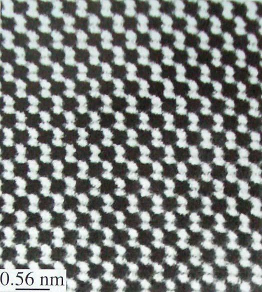
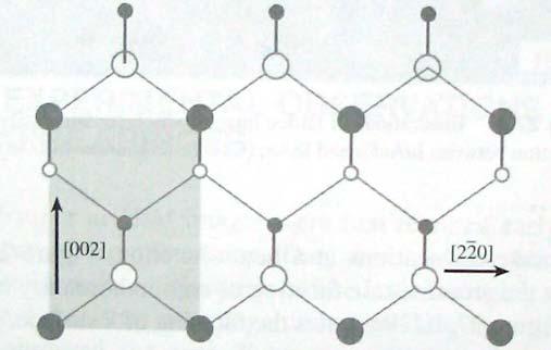
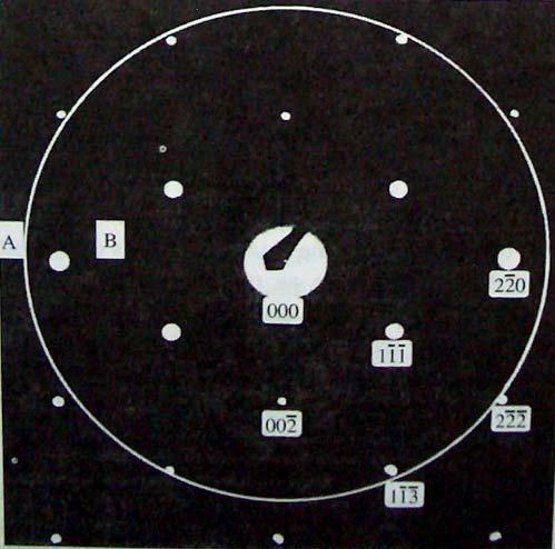
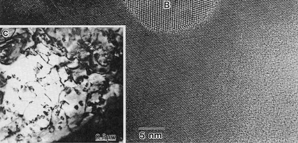
Dislocation networks in graphite
|
|
|
- Diane Robinson
- 5 years ago
- Views:
Transcription


1
2 Dislocation networks in graphite
3
4 High Resolution Microscop With Reference to Lattice Fringe Imaging in a TEM
5 f f r Real space Specimen Reciprocal space hr Point spread function Diffraction pattern Back focal plane F u Hu Contrast transfer function g g r Image Gu Fourier transform
6 u C u f u s r h r f r g u F u H u G Point spread function Convolution in real space gives multiplication in reciprocal space Contrast transfer function Aperture function Envelope function Aberration function u B u E A u u H Propert of lens s C u f f u ] ep[ u i u B Specimen transmission function Phase distortion function
7 High resolution implies abilit to see two closel spaced features in the sample real r space as distinct This corresponds to high spatial frequencies large distances from the optic ais in the diffraction pattern reciprocal u space Ras which pass through the lens at such large distances are bent through a larger angle b the objective lens Due to an imperfect lens spherical aberration these ras are not focused at the same point b the lens Point in the sample disc in the image spreading of a point in the image Objective lens magnifies the image but confuses the detail hence the resolution is limited Each point in the final image has contributions from man points in the specimen no linear relation between the specimen and the image Is a linear relationship possible?
8 i e A f f specimen function phase function of Vz Vz specimen potential V t projected potential Interaction constant =/E Phase Object approimation i e f Weak Phase Object appro. 1 V f t d Vz Specimen Phase change = fv t V i t e f WPOA For a ver thin specimen the amplitude of the transmitted wave function will be linearl related to the projected potential Specimen and approimations ] [ V i t e f dz z V V t V V E d t t Including absorption
9 mee h 2 In vacuum 2 ' z V E me h In the specimen dz dz d 2 2 ' Phase change dz z V E d dz z V d dz z V V t V V E d t t Interaction constant =/E tends to a constant value as V increases energ of electron proportional to E & 1 variables tend to compensate ! 2! 3! 4! e
10 POA holds good onl for thin specimens If specimen is ver thin {V t << 1} WPOA In WPOA {f = 1 i V t } the amplitude of the transmitted wave will be linearl related to the projected potential of the specimen
11 g r f r h r WPOA [1 Vt ] h [1 Vt ] [ Cos i Sin ] I = * Neglecting 2 I [12 V ] Sin t Onl imaginar part of Bu contributes to intensit B u ep[ i u] B u 2Sin[ u]
12 Objective lens transfer function T u A u E u 2Sin[ u] Approimatel T u 2A u Sin[ u] T Or effective u T u E chromatic E spatial coherence Incoherent illumination Tu = Hu Tu ve +ve phase contrast atoms would appear dark In WPOA Tu is sometimes called CTF Envelope is like a virtual aperture at the back focal plane
13 v T u 2A u Sin[ u] +2 C s = 1 mm E 0 = 200 kev f = 58 nm Tu = 2 Sin Å 2 u nm 1
14 1 Scherzer defocus and Information Limits 4 2 fscherzer Cs 3 Tu = 2 Sin T effective u C s = 2.2 mm E 0 = 200 kev f = -100 nm T u 2A u Sin[ u] T effective u nm 1 u T u E u nm 1 chromatic E Damping envelope spatial coherence Scherzer s u =1.51 C r Scherzer = 0.66 C s Instrumental resolution limit can use nearl intuitive arguments to interpret the contrast Information limit


15 IMAGE SIMULATION a b Computer simulation a and electron micrograph b of a Cu Cubeoctahedron consisting of seven shells 1415 atoms in [001] orientation. Structures of nanoclusters b high-resolution transmission electron microscop b J. Urban Volume 10 p.161 in Encclopedia of Nanoscience and Nanotechnolog Ed.: Hari Singh Nalva American Scientific Publishers Stevenson Ranch 2004.


16 Defocus dependenc of lattice images of a Si crstal 200 kv t = 6 nm. Thickness changes from 20 nm a to 90 nm l in steps of 10 nm. High-Resolution Electron Microscop for Materials Science b Daisuke Shindo and Kenji Hiraga Springer-Verlag Toko Thickness dependenc of lattice images of a Si crstal 200 kv f = 65 nm. Thickness changes from 1nm a to 86 nm r in steps of 5 nm. High-Resolution Electron Microscop for Materials Science b Daisuke Shindo and Kenji Hiraga Springer-Verlag Toko 1998.
17 HRTEM- some tips In lattice fringe imaging mode: Things which look like atoms are not atoms! Use image simulation to confirm what ou see Do not interpret details below the resolution limit of the microscope
18 ADVANCES Spherical aberration correctors for illumination as well as imaging lens sstems Electron beam monochromators reducing the energ spread of the electron beam to < 0.1 ev High-energ resolution spectrometers Sub-eV mandoline filter for EELS Imaging energ filters Advanced specimen holders for in-situ eperiments High-sensitivit and high-dnamic-range detectors for images diffraction patterns electron energ loss spectra EELS and energ dispersive X-ra spectra EDXS Advanced methods Focal series reconstruction Electron Holograph In-focus Fresnel reconstruction It is possible to record phase contrast images with point resolutions of well below 0.1 nm or alternativel scan electron probes of size < 0.1 nm across the specimen recording high-angle scattering or high-energ resolution spectra from areas as small as a single atomic column.
![ELECTRON HOLOGRAPHY a b High-resolution a amplitude and b phase images of the aberration-corrected object wave reconstructed from an electron hologram of [110] Si](/docs-images/85/92045143/images/19-0.jpg "obtained at 300 kv on a CM 30 FEG TEM. The characteristic Si dumbbell structure is visible onl after aberration correction. A. Orchowski et al. Phs. Rev. Lett.")
19 ELECTRON HOLOGRAPHY a b High-resolution a amplitude and b phase images of the aberration-corrected object wave reconstructed from an electron hologram of [110] Si obtained at 300 kv on a CM 30 FEG TEM. The characteristic Si dumbbell structure is visible onl after aberration correction. A. Orchowski et al. Phs. Rev. Lett


20 FRESNEL RECONSTRUCTION RT A 2.3 nm RT HT Cooled to RT A 20 HTnm B 2.5 nm B Cooled to RT 20 nm C 3.2 nm 20 nm C Distance Å Eit face wave reconstructed profiles of the imaginar part of the inner potential using zero-defocus Fresnel fringe images

21 NANOSTRUCTURES IMAGE GALLERY


22 NANOTUBES HRTEM image of a BN multi-walled nanotube inner shell distance of ~ 0.33 nm. D. Golberg et al. J. of Appl. Phs a b c HRTEM micrographs of MWNT: a 5-walled diameter = 6.7 nm; b 2-walled diamter = 5.5 nm; c seven-walled diameter = 6.5 nm hollow diameter = 2.2 nm. S. Iijima Nature 354 p


23 NANOLAYERS a b Cross section of TiN/NbN nanolaered coatings: a Conventional TEM micrograph with SAD patterns b HRTEM of {200} lattice fringes. M. Shinn et al. J. Mater. Res
![NANOPARTICLES [001] [110]](/docs-images/85/92045143/images/24-0.jpg "High-resolution micrograph of Si 3 N 4")


24 NANOPARTICLES [001] [110] High-resolution micrograph of Si 3 N 4 TiN composite prepared b CVD. High-Resolution Electron Microscop for Materials Science b Daisuke Shindo and Kenji Hiraga Springer-Verlag Toko a b Gas atomized Al-Si powders: a HREM b SEM c BFI. High-Resolution Electron Microscop for Materials Science b Daisuke Shindo and Kenji Hiraga Springer-Verlag Toko c [110] Al


25 NANOTWINS Twin Plane HREM of ZrO2 showing formation of nanotwins. High-Resolution Electron Microscop for Materials Science b Daisuke Shindo and Kenji Hiraga Springer-Verlag Toko [0 11]


26 NANOpolCRYSTALLINE MATERIAL HREM image of nanocrstalline Pd G.J. Thomas et al. Scripta Metall. Mater


27 MOIRÉ FRINGES HRTEM image of a Kr nanocluster on a Mg substrate showing Moiré fringes. The lattice parameter of Kr can be calculated from the Moiré fringe spacing: [1/d fringes = 1/d MgO 1/d Kr ] Encclopedia of Nanoscience and Nanotechnolog Ed.: Hari Singh Nalva American Scientific Publishers Stevenson Ranch 2004.


28 Intergranular Glass Film High-Angle Annular Dark Field Imaging Incident convergent beam θ 1 > 50 mrad off ais θ 2 >10-50 mrad θ 3 < 10 mrad Specimen θ 1 HAADF detector θ 3 θ 2 BF detector ADF detector HAADF-STEM images of the interface between the IGF and the prismatic surface of an -Si 3 N 4 grain. N. Shibata S.J. Penncook T.R. Gosnell G.S. Painter W.A. Shelton P.F. Becher Observation of rare-earth segregation in silicon nitride ceramics at subnanometre dimensions Nature
29
CHEM-E5225 :Electron Microscopy Imaging
 CHEM-E5225 :Electron Microscopy Imaging 2016.10 Yanling Ge Outline Planar Defects Image strain field WBDF microscopy HRTEM information theory Discuss of question homework? Planar Defects - Internal Interface
High-Resolution. Transmission. Electron Microscopy
 Part 4 High-Resolution Transmission Electron Microscopy 186 Significance high-resolution transmission electron microscopy (HRTEM): resolve object details smaller than 1nm (10 9 m) image the interior of
Chapter 4 Imaging Lecture 24
 Chapter 4 Imaging Lecture 4 d (110) Final Exam Notice Time and Date: :30 4:30 PM, Wednesday, Dec. 10, 08. Place: Classroom CHEM-10 Coverage: All contents after midterm Open note Term project is due today
Transmission Electron Microscopy
 L. Reimer H. Kohl Transmission Electron Microscopy Physics of Image Formation Fifth Edition el Springer Contents 1 Introduction... 1 1.1 Transmission Electron Microscopy... 1 1.1.1 Conventional Transmission
Experimental methods in Physics. Electron Microscopy. Basic Techniques (MEP-I) SEM, TEM
 SEM, TEM") Experimental methods in Physics Electron Microscopy Basic Techniques (MEP-I) SEM, TEM Advanced Techniques (MEP-II) HR-TEM, STEM Analytical-TEM 3D-Microscopy Spring 2012 Experimental Methods in Physics
Experimental methods in Physics Electron Microscopy Basic Techniques (MEP-I) SEM, TEM Advanced Techniques (MEP-II) HR-TEM, STEM Analytical-TEM 3D-Microscopy Spring 2012 Experimental Methods in Physics
CHEM 681 Seminar Mingqi Zhao April 20, 1998 Room 2104, 4:00 p.m. High Resolution Transmission Electron Microscopy: theories and applications
 CHEM 681 Seminar Mingqi Zhao April 20, 1998 Room 2104, 4:00 p.m. High Resolution Transmission Electron Microscopy: theories and applications In materials science, people are always interested in viewing
Supplementary Figure 1: Example non-overlapping, binary probe functions P1 (~q) and P2 (~q), that add to form a top hat function A(~q).
 and P2 (~q), that add to form a top hat function A(~q).") Supplementary Figures P(q) A(q) + Function Value P(q) qmax = Supplementary Figure : Example non-overlapping, binary probe functions P (~q) and P (~q), that add to form a top hat function A(~q). qprobe
Supplementary Figures P(q) A(q) + Function Value P(q) qmax = Supplementary Figure : Example non-overlapping, binary probe functions P (~q) and P (~q), that add to form a top hat function A(~q). qprobe
IMAGING DIFFRACTION SPECTROSCOPY
 TEM Techniques TEM/STEM IMAGING DIFFRACTION SPECTROSCOPY Amplitude contrast (diffracion contrast) Phase contrast (highresolution imaging) Selected area diffraction Energy dispersive X-ray spectroscopy
Techniques EDX, EELS et HAADF en TEM: possibilités d analyse et applications
 Techniques EDX, EELS et HAADF en TEM: possibilités d analyse et applications Thomas Neisius Université Paul Cézanne Plan Imaging modes HAADF Example: supported Pt nanoparticles Electron sample interaction
Spatial Frequency and Transfer Function. columns of atoms, where the electrostatic potential is higher than in vacuum
 Image Formation Spatial Frequency and Transfer Function consider thin TEM specimen columns of atoms, where the electrostatic potential is higher than in vacuum electrons accelerate when entering the specimen
Linear Systems. : object : image. Describes the output of a linear system. input. output. Impulse response function
 Linear Systems Describes the output of a linear system Gx FxHx- xdx FxHx F x G x x output input Impulse response function H x xhx- xdx x If the microscope is a linear system: : object : image G x S F x
Supplementary Information
 Supplementary Information Direct observation of crystal defects in an organic molecular crystals of copper hexachlorophthalocyanine by STEM-EELS Mitsutaka Haruta*, Hiroki Kurata Institute for hemical Research,
Aberration-corrected TEM studies on interface of multilayered-perovskite systems
 Aberration-corrected TEM studies on interface of multilayered-perovskite systems By Lina Gunawan (0326114) Supervisor: Dr. Gianluigi Botton November 1, 2006 MSE 702(1) Presentation Outline Literature Review
Microscopy: Principles
 Low Voltage Electron Microscopy: Principles and Applications Edited by David C. Bell Harvard University, USA and Natasha Erdman JEOL USA Inc., USA Published in association with the Royal Microscopical
AP5301/ Name the major parts of an optical microscope and state their functions.
 Review Problems on Optical Microscopy AP5301/8301-2015 1. Name the major parts of an optical microscope and state their functions. 2. Compare the focal lengths of two glass converging lenses, one with
MSE 321 Structural Characterization
 Auger Spectroscopy Auger Electron Spectroscopy (AES) Scanning Auger Microscopy (SAM) Incident Electron Ejected Electron Auger Electron Initial State Intermediate State Final State Physical Electronics
April 10th-12th, 2017
 Thomas LaGrange, Ph.D. Faculty Lecturer and Senior Staff Scientist Introduction: Basics of Transmission Electron Microscopy (TEM) TEM Doctoral Course MS-637 April 10th-12th, 2017 Outline 1. What is microcopy?
Characterization of crystallographic defects in LaNiO 3 through TEM image simulations
 Characterization of crystallographic defects in LaNiO 3 through TEM image simulations Author: Joan Carles Bastons Garcia. Departament d Electrònica, Universitat de Barcelona Advisors: Sònia Estradé Albiol
Transmission Electron Microscopy and Diffractometry of Materials
 Brent Fultz James Howe Transmission Electron Microscopy and Diffractometry of Materials Fourth Edition ~Springer 1 1 Diffraction and the X-Ray Powder Diffractometer 1 1.1 Diffraction... 1 1.1.1 Introduction
Overview of scattering, diffraction & imaging in the TEM
 Overview of scattering, diffraction & imaging in the TEM Eric A. Stach Purdue University Scattering Electrons, photons, neutrons Radiation Elastic Mean Free Path (Å)( Absorption Length (Å)( Minimum Probe
Chapter 9. Electron mean free path Microscopy principles of SEM, TEM, LEEM
 Chapter 9 Electron mean free path Microscopy principles of SEM, TEM, LEEM 9.1 Electron Mean Free Path 9. Scanning Electron Microscopy (SEM) -SEM design; Secondary electron imaging; Backscattered electron
Transmission Electron Microscopy. Part #2 High Resolution Imaging XEDS EELS spectroscopies Aberration corrected TEM
 Transmission Electron Microscopy Part #2 High Resolution Imaging XEDS EELS spectroscopies Aberration corrected TEM Nicolas Menguy Institut de Minéralogie, de Physique des Matériaux et de Cosmochimie Part
Elastic and Inelastic Scattering in Electron Diffraction and Imaging
 Elastic and Inelastic Scattering in Electron Diffraction and Imaging Contents Introduction Symbols and definitions Part A Diffraction and imaging of elastically scattered electrons Chapter 1. Basic kinematical
Imaging Metrics. Frequency response Coherent systems Incoherent systems MTF OTF Strehl ratio Other Zemax Metrics. ECE 5616 Curtis
 Imaging Metrics Frequenc response Coherent sstems Incoherent sstems MTF OTF Strehl ratio Other Zema Metrics Where we are going with this Use linear sstems concept of transfer function to characterize sstem
Structure analysis: Electron diffraction LEED TEM RHEED
 Structure analysis: Electron diffraction LEED: Low Energy Electron Diffraction SPA-LEED: Spot Profile Analysis Low Energy Electron diffraction RHEED: Reflection High Energy Electron Diffraction TEM: Transmission
High-Resolution Transmission Electron Microscopy
 Chapter 2 High-Resolution Transmission Electron Microscopy The most fundamental imaging mode of a transmission electron microscope is realized by illuminating an electron-transparent specimen with a broad
Energy-Filtering. Transmission. Electron Microscopy
 Part 3 Energy-Filtering Transmission Electron Microscopy 92 Energy-Filtering TEM Principle of EFTEM expose specimen to mono-energetic electron radiation inelastic scattering in the specimen poly-energetic
Conventional Transmission Electron Microscopy. Introduction. Text Books. Text Books. EMSE-509 CWRU Frank Ernst
 Text Books Conventional Transmission Electron Microscopy EMSE-509 CWRU Frank Ernst D. B. Williams and C. B. Carter: Transmission Electron Microscopy, New York: Plenum Press (1996). L. Reimer: Transmission
PROBE AND OBJECT FUNCTION RECONSTRUCTION IN INCOHERENT SCANNING TRANSMISSION ELECTRON MICROSCOPE IMAGING
 Scanning Microscopy Vol. 11, 1997 (Pages 81-90) 0891-7035/97$5.00+.25 Scanning Microscopy International, Chicago Probe (AMF and O Hare), object IL function 60666 reconstruction USA PROBE AND OBJECT FUNCTION
Chemical Analysis in TEM: XEDS, EELS and EFTEM. HRTEM PhD course Lecture 5
 Chemical Analysis in TEM: XEDS, EELS and EFTEM HRTEM PhD course Lecture 5 1 Part IV Subject Chapter Prio x-ray spectrometry 32 1 Spectra and mapping 33 2 Qualitative XEDS 34 1 Quantitative XEDS 35.1-35.4
Transmission Electron Microscopy. Part #1 Diffraction Conventional Imaging
 Transmission Electron Microscopy Part #1 Diffraction Conventional Imaging Nicolas Menguy Institut de Minéralogie, de Physique des Matériaux et de Cosmochimie Outline Part 1 : Conventional TEM - Transmission
Detecting strain in scanning transmission electron microscope images. Part II Thesis
 Detecting strain in scanning transmission electron microscope images Part II Thesis Ina M. Sørensen Mansfield College, Oxford 10th of June, 2015 1 Abstract Scanning Transmission Electron Microscopes (STEM)
Praktikum zur. Materialanalytik
 Praktikum zur Materialanalytik Energy Dispersive X-ray Spectroscopy B513 Stand: 19.10.2016 Contents 1 Introduction... 2 2. Fundamental Physics and Notation... 3 2.1. Alignments of the microscope... 3 2.2.
Transmission Electron Microscopy for metrology and characterization of semiconductor devices
 Transmission Electron Microscopy for metrology and characterization of semiconductor devices Bert Freitag, Laurens Kwakman, Ivan Lazic and Frank de Jong FEI / ThermoFisher Scientific, Achtseweg Noord 5,
EELS Electron Energy Loss Spectroscopy
 EELS Electron Energy Loss Spectroscopy (Thanks to Steve Pennycook, Quan Li, Charlie Lyman, Ondre Krivenak, David Muller, David Bell, Natasha Erdman, Nestor Zaluzec and many others) Nestor Zaluzec,
Chapter 4 Imaging. Lecture 21. d (110) Chem 793, Fall 2011, L. Ma
 Chem 793, Fall 2011, L. Ma") Chapter 4 Imaging Lecture 21 d (110) Imaging Imaging in the TEM Diraction Contrast in TEM Image HRTEM (High Resolution Transmission Electron Microscopy) Imaging or phase contrast imaging STEM imaging a
Chapter 4 Imaging Lecture 21 d (110) Imaging Imaging in the TEM Diraction Contrast in TEM Image HRTEM (High Resolution Transmission Electron Microscopy) Imaging or phase contrast imaging STEM imaging a
PHYS-E0541:Special Course in Physics Gas phase synthesis of carbon nanotubes for thin film application. Electron Microscopy. for
 PHYS-E0541:Special Course in Physics Gas phase synthesis of carbon nanotubes for thin film application Electron Microscopy for Introduction to Electron Microscopy Carbon Nanomaterials (nanotubes) Dr. Hua
Weak-Beam Dark-Field Technique
 Basic Idea recall bright-field contrast of dislocations: specimen close to Bragg condition, s î 0 Weak-Beam Dark-Field Technique near the dislocation core, some planes curved to s = 0 ) strong Bragg reflection
sin" =1.22 # D "l =1.22 f# D I: In introduction to molecular electron microscopy - Imaging macromolecular assemblies
 I: In introduction to molecular electron microscopy - Imaging macromolecular assemblies Yifan Cheng Department of Biochemistry & Biophysics office: GH-S472D; email: ycheng@ucsf.edu 2/20/2015 - Introduction
Transmission Electron Microscope. Experimental Instruction
 Transmission Electron Microscope Experimental Instruction In advanced practical course [F-Praktikum] Date: April 2017 Contents 1 Task 3 2 Theoretical Basics 3 2.1 Bragg Diffraction......................................
Setting The motor that rotates the sample about an axis normal to the diffraction plane is called (or ).
.") X-Ray Diffraction X-ray diffraction geometry A simple X-ray diffraction (XRD) experiment might be set up as shown below. We need a parallel X-ray source, which is usually an X-ray tube in a fixed position
X-Ray Diffraction X-ray diffraction geometry A simple X-ray diffraction (XRD) experiment might be set up as shown below. We need a parallel X-ray source, which is usually an X-ray tube in a fixed position
Resolution of coherent and incoherent imaging systems reconsidered - Classical criteria and a statistical alternative
 Resolution of coherent and incoherent imaging systems reconsidered - Classical criteria and a statistical alternative Sandra Van Aert and Dirk Van Dyck University of Antwerp, Department of Physics, Groenenborgerlaan
Supplementary Information
 Supplementary Information Supplementary Figures Supplementary figure S1: Characterisation of the electron beam intensity profile. (a) A 3D plot of beam intensity (grey value) with position, (b) the beam
Physical Principles of Electron Microscopy. 2. Electron Optics
 Physical Principles of Electron Microscopy 2. Electron Optics Ray Egerton University of Alberta and National Institute of Nanotechnology Edmonton, Canada www.tem-eels.ca regerton@ualberta.ca Properties
SIMULATION OF TRANSMISSION AND SCANNING TRANSMISSION ELECTRON MICROSCOPIC IMAGES CONSIDERING ELASTIC AND THERMAL DIFFUSE SCATTERING
 Scanning Microscopy Vol. 11, 1997 (Pages 277-286) 0891-7035/97$5.00+.25 Scanning Microscopy International, Chicago (AMF Simulation O Hare), of TEM IL 60666 and STEM USA images SIMULATION OF TRANSMISSION
Optics.
 Optics www.optics.rochester.edu/classes/opt100/opt100page.html Course outline Light is a Ray (Geometrical Optics) 1. Nature of light 2. Production and measurement of light 3. Geometrical optics 4. Matrix
DIFFRACTION PHYSICS THIRD REVISED EDITION JOHN M. COWLEY. Regents' Professor enzeritus Arizona State University
 DIFFRACTION PHYSICS THIRD REVISED EDITION JOHN M. COWLEY Regents' Professor enzeritus Arizona State University 1995 ELSEVIER Amsterdam Lausanne New York Oxford Shannon Tokyo CONTENTS Preface to the first
PRINCIPLES OF PHYSICAL OPTICS
 PRINCIPLES OF PHYSICAL OPTICS C. A. Bennett University of North Carolina At Asheville WILEY- INTERSCIENCE A JOHN WILEY & SONS, INC., PUBLICATION CONTENTS Preface 1 The Physics of Waves 1 1.1 Introduction
Energy-Filtered High-Resolution Electron Microscopy for Quantitative Solid State Structure Determination
 [J. Res. Natl. Inst. Stand. Technol. 102, 1 (1997)] Energy-Filtered High-Resolution Electron Microscopy for Quantitative Solid State Structure Determination Volume 102 Number 1 January February 1997 Z.
Electron microscopy in molecular cell biology I
 Electron microscopy in molecular cell biology I Electron optics and image formation Werner Kühlbrandt Max Planck Institute of Biophysics chemistry biology Objects of interest Galaxy 10 6 light years 10
Chapter 10. Nanometrology. Oxford University Press All rights reserved.
 Chapter 10 Nanometrology Oxford University Press 2013. All rights reserved. 1 Introduction Nanometrology is the science of measurement at the nanoscale level. Figure illustrates where nanoscale stands
Nanoelectronics 09. Atsufumi Hirohata Department of Electronics. Quick Review over the Last Lecture
 Nanoelectronics 09 Atsufumi Hirohata Department of Electronics 13:00 Monday, 12/February/2018 (P/T 006) Quick Review over the Last Lecture ( Field effect transistor (FET) ): ( Drain ) current increases
Controllable Atomic Scale Patterning of Freestanding Monolayer. Graphene at Elevated Temperature
 Controllable Atomic Scale Patterning of Freestanding Monolayer Graphene at Elevated Temperature AUTHOR NAMES Qiang Xu 1, Meng-Yue Wu 1, Grégory F. Schneider 1, Lothar Houben 2, Sairam K. Malladi 1, Cees
November 30th -December 2 nd, st 2nd 3rd. 8:15 7)HRTEM 10) TEM imaging and diffraction examples. 9:15 8)HRTEM 10) Diffraction going further
HRTEM 10) TEM imaging and diffraction examples. 9:15 8)HRTEM 10) Diffraction going further") Thomas LaGrange, Ph.D. Faculty and Staff Scientist Introduction: Basics of Transmission Electron Microscopy (TEM) TEM Doctoral Course MS-637 November 30th -December 2 nd, 2015 Planning MSE-637 TEM -basics
Thomas LaGrange, Ph.D. Faculty and Staff Scientist Introduction: Basics of Transmission Electron Microscopy (TEM) TEM Doctoral Course MS-637 November 30th -December 2 nd, 2015 Planning MSE-637 TEM -basics
Electron Microscopy I
 Characterization of Catalysts and Surfaces Characterization Techniques in Heterogeneous Catalysis Electron Microscopy I Introduction Properties of electrons Electron-matter interactions and their applications
Part 3 - Image Formation
 Part 3 - Image Formation Three classes of scattering outcomes Types of electron microscopes Example SEM image: fly nose Example TEM image: muscle Skeletal muscle. Cell and Tissue Ultrastructure Mercer
MSE 321 Structural Characterization
 Auger Spectroscopy Auger Electron Spectroscopy (AES) Scanning Auger Microscopy (SAM) Incident Electron Ejected Electron Auger Electron Initial State Intermediate State Final State Physical Electronics
The Principles of STEM Imaging
 2 The Principles of STEM Imaging Peter D. Nellist 2.1 Introduction The purpose of this chapter is to review the principles underlying imaging in the scanning transmission electron microscope (STEM). Consideration
Supplementary Information
 Supplementary Information Supplementary Figure 1. X-ray diffraction patterns of (a) pure LDH, (b) AuCl 4 ion-exchanged LDH and (c) the Au/LDH hybrid catalyst. The refined cell parameters for pure, ion-exchanged,
MSE 321 Structural Characterization
 Optical Microscope Plan Lenses In an "ideal" single-element lens system all planar wave fronts are focused to a point at distance f from the lens; therefore: Image near the optical axis will be in perfect
Chapter 12. Nanometrology. Oxford University Press All rights reserved.
 Chapter 12 Nanometrology Introduction Nanometrology is the science of measurement at the nanoscale level. Figure illustrates where nanoscale stands in relation to a meter and sub divisions of meter. Nanometrology
Supplementary information
 Supplementary information Supplementary Figures Supplementary Figure 1. CO 2 light off curve obtained from the 5 wt% Pt/Al 2 O 3 catalyst obtained through heating the catalyst under a 50 ml.min -1 flow
This article appeared in a journal published by Elsevier. The attached copy is furnished to the author for internal non-commercial research and
 This article appeared in a journal published by Elsevier. The attached copy is furnished to the author for internal non-commercial research and education use, including for instruction at the authors institution
Lecture 6. What is contrast? Eyes: < 5% - can t detect <10% - difficult Enhance digital image electronically I I C I
 Phae Contrat Lecture 6 Scattering/Amplitude Contrat BF/DF: thickne, tilt Low-medium magnification Application Crytal defect: dilocation, tacking fault, phae boundarie, precipitate, defect cluter Contrat:
On the use of Kumakhov Polycapillaries to improve laboratory
 ICXOM Frascati (INFN - LNF) 25-30 September 2005 On the use of Kumakhov Polycapillaries to improve laboratory Energy Dispersive X-ray X Diffractometry and Reflectometry B. Paci 1, V. Rossi Albertini 1,
The Basic of Transmission Electron Microscope. Text book: Transmission electron microscopy by David B Williams & C. Barry Carter.
 The Basic of Transmission Electron Microscope Text book: Transmission electron microscopy by David B Williams & C. Barry Carter. 2009, Springer Background survey http://presemo.aalto.fi/tem1 Microscopy
Molecular electron microscopy
 Molecular electron microscopy - Imaging macromolecular assemblies Yifan Cheng Department of Biochemistry & Biophysics office: GH-S427B; email: ycheng@ucsf.edu 2/22/2013 - Introduction of Molecular Microscopy:
LC circuit: Energy stored. This lecture reviews some but not all of the material that will be on the final exam that covers in Chapters
 Disclaimer: Chapter 29 Alternating-Current Circuits (1) This lecture reviews some but not all of the material that will be on the final exam that covers in Chapters 29-33. LC circuit: Energy stored LC
X-ray diffraction geometry
 X-ray diffraction geometry Setting controls sample orientation in the diffraction plane. most important for single-crystal diffraction For any poly- (or nano-) crystalline specimen, we usually set: 1 X-ray
Chapter 16 Holography
 Chapter 16 Holography Virtually all recording devices for light respond to light intensity. Problem: How to record, and then later reconstruct both the amplitude and phase of an optical wave. [This question
Atomic Resolved HAADF-STEM for Composition Analysis
 Volume 38 Number 2 November 10, 2003 Atomic Resolved HAADF-STEM for Composition Analysis Makoto Shiojiri,, and Takashi. Yamazaki Kanazawa Medical University, Ishikawa 920-0293, Japan Kyoto Institute of
*Specifications subject to change without notice.
 The Power of STEM *Specifications subject to change without notice. No. 1301G040C 1101E010C Printed in Japan, Kp Atomic Resolution Analytical Microscope Serving Advanced Technology Atomic Resolution Analytical
Supporting Information s for
 Supporting Information s for # Self-assembling of DNA-templated Au Nanoparticles into Nanowires and their enhanced SERS and Catalytic Applications Subrata Kundu* and M. Jayachandran Electrochemical Materials
CHARACTERIZATION of NANOMATERIALS KHP
 CHARACTERIZATION of NANOMATERIALS Overview of the most common nanocharacterization techniques MAIN CHARACTERIZATION TECHNIQUES: 1.Transmission Electron Microscope (TEM) 2. Scanning Electron Microscope
Lecture 10: Surface Plasmon Excitation. 5 nm
 Excitation Lecture 10: Surface Plasmon Excitation 5 nm Summary The dispersion relation for surface plasmons Useful for describing plasmon excitation & propagation This lecture: p sp Coupling light to surface
Everhart-Thornley detector
 SEI Detector Everhart-Thornley detector Microscope chamber wall Faraday cage Scintillator Electrons in Light pipe Photomultiplier Electrical signal out Screen Quartz window +200 V +10 kv Always contains
SEM stands for Scanning Electron Microscopy. The earliest known work describing
 1. HISTORY ABOUT SEM SEM stands for Scanning Electron Microscopy. The earliest known work describing the concept of a Scanning Electron Microscope was by M. Knoll (1935) who, along with other pioneers
Main Notation Used in This Book
 Main Notation Used in This Book z Direction normal to the surface x,y Directions in the plane of the surface Used to describe a component parallel to the interface plane xoz Plane of incidence j Label
TrueImage A Software Package for Focal-Series Reconstruction in HRTEM
 TrueImage A Software Package for Focal-Series Reconstruction in HRTEM C. Kübel 1 and A. Thust 2 1) FEI Company, Achtseweg Noord 5, 5651 GG Eindhoven, The Netherlands. 2) Forschungszentrum Jülich GmbH,
Characterisation of Nanoparticles using Advanced Electron Microscopy
 Wright State University CORE Scholar Special Session 5: Carbon and Oxide Based Nanostructured Materials (2013) Special Session 5 6-2013 Characterisation of Core@Shell Nanoparticles using Advanced Electron
Introduction to EDX. Energy Dispersive X-ray Microanalysis (EDS, Energy dispersive Spectroscopy) Basics of EDX
 Basics of EDX") Introduction to EDX Energy Dispersive X-ray Microanalysis (EDS, Energy dispersive Spectroscopy) EDX Marco Cantoni 1 Basics of EDX a) Generation of X-rays b) Detection Si(Li) Detector, SDD Detector, EDS
Introduction to EDX Energy Dispersive X-ray Microanalysis (EDS, Energy dispersive Spectroscopy) EDX Marco Cantoni 1 Basics of EDX a) Generation of X-rays b) Detection Si(Li) Detector, SDD Detector, EDS
(Supporting Information)
") Atomic and Electronic Structure of Graphene-Oxide (Supporting Information) K. Andre Mkhoyan, 1,2 * Alexander W. Contryman, 1 John Silcox, 1 Derek A. Stewart, 3 Goki Eda, 4 Cecilia Mattevi, 4 Steve Miller,
Atomic and Electronic Structure of Graphene-Oxide (Supporting Information) K. Andre Mkhoyan, 1,2 * Alexander W. Contryman, 1 John Silcox, 1 Derek A. Stewart, 3 Goki Eda, 4 Cecilia Mattevi, 4 Steve Miller,
= 6 (1/ nm) So what is probability of finding electron tunneled into a barrier 3 ev high?
 So what is probability of finding electron tunneled into a barrier 3 ev high?") STM STM With a scanning tunneling microscope, images of surfaces with atomic resolution can be readily obtained. An STM uses quantum tunneling of electrons to map the density of electrons on the surface
STM STM With a scanning tunneling microscope, images of surfaces with atomic resolution can be readily obtained. An STM uses quantum tunneling of electrons to map the density of electrons on the surface
Synthesis of Colloidal Au-Cu 2 S Heterodimers via Chemically Triggered Phase Segregation of AuCu Nanoparticles
 SUPPORTING INFORMATION Synthesis of Colloidal Au-Cu 2 S Heterodimers via Chemically Triggered Phase Segregation of AuCu Nanoparticles Nathan E. Motl, James F. Bondi, and Raymond E. Schaak* Department of
Supplementary Information: Twinning of cubic diamond explains reported nanodiamond polymorphs
 Supplementary Information: Twinning of cubic diamond explains reported nanodiamond polymorphs Péter Németh 1, Laurence A.J. Garvie 2,3, and Peter R. Buseck 3, 4 1 Institute of Materials and Environmental
Practical course in scanning electron microscopy
 Practical course in scanning electron microscopy Fortgeschrittenen Praktikum an der Technischen Universität München Wintersemester 2017/2018 Table of contents 1. Introduction 3 2. Formation of an electron
QUANTUM PHYSICS. Limitation: This law holds well only for the short wavelength and not for the longer wavelength. Raleigh Jean s Law:
 Black body: A perfect black body is one which absorbs all the radiation of heat falling on it and emits all the radiation when heated in an isothermal enclosure. The heat radiation emitted by the black
Phase microscopy: Fresnel fringes in the TEM
 Phase microscopy: Fresnel fringes in the TEM Interferences between waves not being in phase overfocussed 2 waves propagating through different media (sample, vacuum) => difference of mean inner potentials
Sub-Angstrom Edge Relaxations Probed by Electron. Microscopy in Hexagonal Boron Nitride (h-bn)
") Supplementary Material for Sub-Angstrom Edge Relaxations Probed by Electron Microscopy in Hexagonal Boron Nitride (h-bn) Nasim Alem 1,2,3, Quentin M. Ramasse 4,*, Che R. Seabourne 5, Oleg V. Yazyev 1,3,6,
Supplementary Material for Sub-Angstrom Edge Relaxations Probed by Electron Microscopy in Hexagonal Boron Nitride (h-bn) Nasim Alem 1,2,3, Quentin M. Ramasse 4,*, Che R. Seabourne 5, Oleg V. Yazyev 1,3,6,
Setup of the apparatus and details of deposition process
 Dense growth of multiply-twinned star-shaped molybdenum particles by atmospheric H 2 /Ar microplasma jet Yoshiki Shimizu, * Kenji Koga, Takeshi Sasaki, and Naoto Koshizaki Setup of the apparatus and details
Supporting Information. Re-Investigation of the Alleged Formation of CoSi Nanoparticles on Silica. Van An Du, Silvia Gross and Ulrich Schubert
 Supporting Information Re-Investigation of the Alleged Formation of CoSi Nanoparticles on Silica Van An Du, Silvia Gross and Ulrich Schubert Experimental All manipulations were carried out under an atmosphere
Efficient Hydrogen Evolution. University of Central Florida, 4000 Central Florida Blvd. Orlando, Florida, 32816,
 Electronic Supplementary Material (ESI) for Energy & Environmental Science. This journal is The Royal Society of Chemistry 2017 MoS 2 /TiO 2 Heterostructures as Nonmetal Plasmonic Photocatalysts for Highly
X-Ray Diffraction as a key to the Structure of Materials Interpretation of scattering patterns in real and reciprocal space
 X-Ray Diffraction as a key to the Structure of Materials Interpretation of scattering patterns in real and reciprocal space Tobias U. Schülli, X-ray nanoprobe group ESRF OUTLINE 1 Internal structure of
Characterisation of Nanoparticle Structure by High Resolution Electron Microscopy
 Journal of Physics: Conference Series OPEN ACCESS Characterisation of Nanoparticle Structure by High Resolution Electron Microscopy To cite this article: Robert D Boyd et al 2014 J. Phys.: Conf. Ser. 522
Book Review published on American Scientist Vol. 84, 406 (1996).
.") Book Review published on American Scientist Vol. 84, 406 (1996). Elastic and Inelastic Scattering in Electron Diffraction and Imaging, Zhong Lin Wang Plenum Press, 1995. 448 pp. Scientists and engineers
Book Review published on American Scientist Vol. 84, 406 (1996). Elastic and Inelastic Scattering in Electron Diffraction and Imaging, Zhong Lin Wang Plenum Press, 1995. 448 pp. Scientists and engineers
Supporting Information
 Copyright WILEY-VCH Verlag GmbH & Co. KGaA, 69469 Weinheim, Germany, 2015. Supporting Information for Adv. Mater., DOI: 10.1002/adma.201502134 Stable Metallic 1T-WS 2 Nanoribbons Intercalated with Ammonia
Physical Optics. Lecture 3: Fourier optics Herbert Gross.
 Phsical Optics Lecture 3: Fourier optics 8-4-5 Herbert Gross www.iap.uni-jena.de Phsical Optics: Content No Date Subject Ref Detailed Content.4. Wave optics G Comple fields, wave equation, k-vectors, interference,
Supporting Information
 Supporting Information Single-atom and Nano-clustered Pt Catalysts for Selective CO 2 Reduction Yuan Wang, a Hamidreza Arandiyan,* a,b Jason Scott,* a Kondo-Francois Aguey-Zinsou, c and Rose Amal* a Miss
3D and Atomic-resolution Imaging with Coherent Electron Nanobeams - Opportunities and Challenges for X-rays
 3D and Atomic-resolution Imaging with Coherent Electron Nanobeams - Opportunities and Challenges for X-rays David A. Muller Lena Fitting Kourkoutis, Megan Holtz, Robert Hovden, Qingyun Mao, Julia Mundy,
REVIEWS. Resolution and aberration correction in liquid cell transmission electron microscopy
 REVIEWS Resolution and aberration correction in liquid cell transmission electron microscopy Niels de Jonge 1,2, Lothar Houben 3,4, Rafal E. Dunin- Borkowski 3 and Frances M. Ross 5,6 * Abstract Liquid