Chapter 4 Imaging Lecture 24
|
|
|
- Simon Conley
- 6 years ago
- Views:
Transcription

")
1 Chapter 4 Imaging Lecture 4 d (110)
2 Final Exam Notice Time and Date: :30 4:30 PM, Wednesday, Dec. 10, 08. Place: Classroom CHEM-10 Coverage: All contents after midterm Open note Term project is due today
3 Imaging Imaging in the TEM Diffraction Contrast in TEM Image HRTEM (High Resolution Transmission Electron Microscopy) Imaging or phase contrast imaging STEM imaging
4 Basic Imaging Theory 1.The imaging process As a first approximation, we consider coherent image, i.e. a plane parallel, monochromatic electron wave falls in the object, and is scattered, the scattered waves interfere and recombined by an electron lens (objective lens) to form an image.. The process consists of two parts: (a). The interaction of the incident wave with the object, defining the exit wave from the object, transmission function q (x); (b) the action of the objective lens in forming the image, transfer function t (x). ψ(x)= q(x)*t(x), and I (x)= q(x)*t(x) ^ or ψ(u)= Q(u)*T(u). 3. The essential question: how is the images intensity distribution related to the object structure? 4. For detailed discussion of imaging and electron scattering, see Diffraction Physics by John M. Cowley, North-Holland, Amsterdam, 1981, nd edition.
, etc.")
5 Many beams were selected by an aperture (ring) to form image showing more information about the structure of specimen. the question is where are the atoms with respect to the bright and dark contrast dots? Do the dark spots or bright spot correspond what atoms (Ga or As), etc.? Beautiful image sometimes is difficult to interpret. a. Simulation b. SAD pattern c. FFT pattern
6 5. Imaging in WPOA Imaging function ψ I I I ( x) = ( 1 iσv ( x) ) t( x) ( ) ( ) [ ( )] [ ( ) ] iχ u t x = F T u = F A u e = F[ A( u) ( cos χ( u) + i sin χ( u) )] c( x) = F[ A( u) cos χ( u) ] s( x) = F[ A( u) sin χ( u) ] ψ ( x) = ( 1 iσv ( x) ) ( c( x) + is( x) ) ( x) = ψ ( x) ψ ( x) * = ψ ( x) where Let and so ignore high order term, σ ( x) = 1+ σv ( x) s( x)...( a) ( u) = δ ( u) + σq( u) S( u)...( b) The effect of equation (a) is that mulyiplying diffraction pattern in BFP by the phase contrast transfer function S ( u) = F[ s( x) ] = A( u) sin χ( u) or in Fourier space
7 S ( u) = A( u) sin χ( u) where ( ) A u ( ) 1 3 χ u = π fλu + πcsλ u u = θ / λ, reciprocal vector χ ( u) may be called phase distortion function Phase contrast transfer function is aperture function the phase contrast transfer function (PCTF) is oscillatory, showing maximum transfer of contrast when χ(u)=±π/, and zero contrast when χ(u)=±π When S(u) is negative, positive phase contrast results, meaning that atoms would appear dark against a bright background. When S(u) is positive, negative phase contrast results, meaning that atoms would appear bright against a dark background. when S(u) =0, there is no detail in the image for this value of U 4
8 Cs=1. mm, and E=300 kv 1.5 delta f, -58nm delt f, -150 nm delta f, -10nm sinx(u) u (1/nm) u If we fix Cs and E, u increases as f decreases achieving a higher spatial resolution. Further decreasing f will cause u suddenly jump to cross the u-axis and decrease u
9 Scherzer defocus the CTF could be optimized by balancing the effect of spherical aberration against a particular negative of f, called Scherzer defocus. At this defocus, all beams will have nearly constant phase out to the first crossover of the zero axis. This crossover point is defined as the instrumental resolution limit. This is the best performance that can be expected from a microscope unless we use imaging processing method to extract more information. The implications of resolution require as many beams as possible being transferred through the optical system with identical phase.
10 ( ) ( ) Scherzer resolution 3 4 Scherzer defocus and (b) combining (a)...(b) so be near -1 will sin, 3 - when as shown in figure, ) 0...( 0, let 1 λ λ λ π λ π π χ π χ λ λ π λ π λ π λ π χ λ π λ π χ s Sch Sch s s s s s C r Cs f u C u f a u C f u C u f u C u f du u d u C u f u = = + = = = + = + + = + = d c s g p d d d d d = min λ λ α s s optimum C d C = = Based on the electron probe size Resolution

11 (a) (b) Envelop Damping Function The plots of sinχ(u) as a function of u could extend out as far as you want to plot them. In practice, they don t because of the envelop damping function, i.e. the microscope is unable to image the finest detail due to reasons other than the simple transfer characteristics of a linear system. Envelop damping function results in the information retrieval limit or instrumental resolution limit. If we set up the Scherzer defocus or damping function, i.e. whichever equals zero first, the phase-contrast images are directly interpretable. Beyond the limit, we have to use computer simulation for interpretation.

12 The minimum contrast defocus condition all contrast is minimized and cannot see anything in minimum contrast condition : sin χ and ( u) = ( λ) f MC = 0.44 C s Imaging using first passbands using minimum contrast defocus as a reference point, we can adjust the defocus to Scherzer defocus. As shown in figure, the first passband condition settings for CTF allow higher spatial frequencies to contribute to the image, and X is constant or dx/du is small over a range of u which includes the reflection of interest.
13 Cs=1. mm, and E=300 kv delt f, -150 nm sinx(u) u (1/nm) As shown in above figure, we may obtain a pretty picture using high order passbands settings, but it may not give a true structure image of specimen. at the high-order passbands setting, imaging the specimen is beyond the instrumental resolution limit so we cannot use the intuitive approach for image interpretation. we should exactly know where the zeros are in the CTF, and use computer simulation to assist the image interpretation.
14 Simulation of high resolution TEM image Thick specimen Slices Multi-slice method is used to simulate HRTEM image a specimen of thickness, t, is modeled as n slice, and each of thickness is z, or t=n z The crystal potential of each slice is replaced by its two-dimensional projected potential. The effect of the first slice on the phase of incident wave-front is calculated, and the resulting wave function is then propagated through free space to the next slice. This process is repeated until the desire specimen thickness is achieved. Assuming z is sufficiently small, this method is highly accurate.
15 Schematic procedure of simulation of HRTEM

16 Thickness, nm defocus, nm The output of simulation is always in this type of table showing variation of image with thickness and defocus Simulated HRTEM images of a Ti/TiH interface over a range of crystal thickness and defocus values. The zone axis is [0001] of Ti
17 HRSTEM imaging Spectroscopy Other technologies in TEM Basic SEM Review
.")
18 Schematic view of the various signals and their detectors used on a STEM STEM imaging or Z-contrast imaging The Scanning Transmission Electron Microscope ( STEM) provides the facility of scanning a small probe across a specimen in the TEM, comparable to a Scanning Electron Microscope (SEM). The interaction between the electron beam and the specimen generates different signals like transmitted electrons, backscattered electrons, secondary electrons and X-rays, containing information about the actually illuminated part of the specimen. In the STEM, the beam is scanned across the specimen in a rectangular pattern. At the same time, the intensity of one or more signals is measured and translated into brightness values. An image containing specific information about the specimen is collected while scanning the beam. Z-contrast images are formed by collecting high angle ( mrad, an order magnitude larger than Bragg angle) elastically scattered electron with an annular dark field detector ( HAADF).
")

19 Using the STEM detector to form BF and DF image STEM image formation: A Bright Field (BF) detector is placed in a conjugate plane to the back focal plane to intercept the direct beam while a concentric Annular Dark Field (ADF) detector intercepts the diffracted electrons. The signals from either detector are amplified and modulate the STEM CRT. The specimen (Au islands on a C film) gives complementary ADF and BF images as can be seen by clicking the button opposite.
20
 To form coherent CBED pattern and the coherent CBED disks are allowed to overlap STEM image is formed by scanning these overlapped CBED pattern ( nano-probe) Nano-probe to form CBED pattern")
21 CBED mode Ray diagram and beam condition of STEM In the coherent nano-probe mode (sub-nanometer diameter) with the smallest possible probe size ( for filed emission gun d = nm) To form coherent CBED pattern and the coherent CBED disks are allowed to overlap STEM image is formed by scanning these overlapped CBED pattern ( nano-probe) Nano-probe to form CBED pattern STEM mode is good for spectroscopic analysis

22 Small convergent angle, α Ray diagram showing how to form CBED pattern

23 large convergent angle, α The pattern is overlapped due to high convergent angle

24 CBED pattern without overlapping
 without")
25 CBED whole pattern (small camera length) without overlapping
26 CBED pattern with overlapping
27 Lattice imaging in STEM using overlapping CBED orders If CBED orders overlap, and if the angular range over which the illumination is coherent exceeds the Bragg angle, it becomes possible to form a phase contrast STEM lattice image or called high resolution Z-contrast image. The image is formed by detecting part of the CBED pattern ( the overlap region) and by displaying this intensity as a function of probe position, as the probe is scanned over the sample. As shown in figure, two illumination angles allow the overlap of CBED, so a detector at D record a twobeam lattice image as the probe is scanned. Interchanging S and D point shows that this is equivalent to inclined illumination TEM lattice imaging. This is called reciprocity theorem, which states if we swap a point source of illumination between the TEM and the STEM configurations, the intensity at the detector will be the same. In STEM, the focusing of incident electrons into a small spot requires converging ray paths, in analogy to the requirement in TEM that rays are included that have undergone scattering to large diffracted vector and contain information on short spatial periodicities.

28 Axial three-beam lattice imaging in STEM. By opening up the illumination angle to twice the Bragg angle, three orders overlap at the axial detector D. The appearance of a two-dimensional coherent CBED pattern used for axial five-beam lattice imaging is shown at the right
29 Reciprocity theorem applied to TEM and STEM: If the direction of electrons in STEM is reversed and the source and detector interchanged, then the BF-STEM and the TEM are identical. the image in the BF-STEM is equivalent to the BF image in the CTEM. ADF-STEM image would be equivalent to the BF-TEM image using incoherent hollow cone illumination.
30 A B Idealized relationship between two imaging modes: the wave amplitude at point B in a system due to a point source at point A is the same as the amplitude that would be produced at A by a point source at B. All contrast mechanism possible in CTEM are also possible in STEM, I,e, phase contrast, diffraction contrast, Fresnel fringes etc.
31 Rutherford Scattering The relative angular distribution of the transmitted electrons With a HAADF detector, the scattered electron to extreme large angle are collected and form a Z-contrast image.
![Mechanism of STEM imaging The specimen in (a) consists of an array of atomic columns ([110] Si for example), for which the potential for high-angle scattering can be represented by an object function](/docs-images/77/74872274/images/32-0.jpg "consisting of weighted spikes, as in (b). The STEM image can ed interpreted as a convolution of the nano-probe and the objection function, as in (c).")
32 Mechanism of STEM imaging The specimen in (a) consists of an array of atomic columns ([110] Si for example), for which the potential for high-angle scattering can be represented by an object function consisting of weighted spikes, as in (b). The STEM image can ed interpreted as a convolution of the nano-probe and the objection function, as in (c). As probe scans, it maps out the spikes, producing a direct image of high-angle scattering power. It acts as the single probe lightens up the bulbs (atom columns) while scanning. The bright spots are location of atoms. Comparing to HRTEM, the resolution in STEM imaging is less affected by phase errors induced by objective lens. The incoherence of the STEM images (or Z-contrast image) is a consequence of their large K (scattering vector). For the incoherent imaging, we sum the intensities, I, from the atoms, rather than the wave-function amplitudes, ψ, from the atoms as in coherent HRTEM imaging. Each atom can be considered as an independent scatter because there is no constructive and destructive interference between the wave amplitudes scattered by the different atoms. At high angles, the scattering scales with atomic number approximately as Z^, as expected for Rutherford scattering from an unscreened nucleus.

33 Mechanism of STEM imaging (cont ) When the probe is smaller than the spacing of aligned atomic columns in a crystal, the atom columns are illuminated sequentially as the probe is scanned over the specimen. This Z-dependence scattering carries composition information about specimen independent of the geometry of the unit cell and the presence of forbidden diffractions or defects. The interpretation of the Z-contrast image is almost intuitive.
 Changing the focus of")


34 (a) (a). Simulated defocus series for Si<110> with corresponding probe intensity profiles STEM image and simulated Si dumbbells structure Mechanism of STEM imaging (cont ) Changing the focus of the objective lens alters the intensity distribution of the probe on the specimen surface as shown in above figure for Si<110>. Near Scherzer defocus, -70 nm, the probe most closely resembles a diffraction-limited Airy disk. At smaller defocus the central peak broadens, and at larger defocus, the central peak sharpens, but more intensity appears in the subsidiary maxima. While these conditions result in significantly different images, the contrast away from Scherzer defocus is reduced substantially in both cases. So in practice, the Scherzer defocus can be found readily. The good contrast image is only from one defocus, allowing intuitive interpretation. As shown in figures, although the expected Si dumbbells are not resolved in this <110> images, by knowing that atoms act as sharp objects, one can infer from the oval shape of the bright spots that at least two atomic columns must be present closer together.
35 STEM imaging theory (1-D) ψ t (u, x p ) the aberration wave function : e max iχ ( u ) ( x, x p ) = Ap e ( x, x ) dx = 1 [ iχ ( u )] The aberrated electron probe wave function in the plane of the specimen when deflected to position x is : ψ A p ψ 0 [ ] [ πiu( x x p )] e du is a normalization constant chosen to yield p ψ t ( x, xp ) is ( x, x ) = t( x) ψ ( x, x ) function form CBEDpattern u the electron probepasses through the specimen and the transmission function is t(x),so the transmitted wave ψ t this wavefunction is then diffractedonto thedetector planeand Ψ p πiux ( u, xp ) = F[ ψ t ( x, xp )] = e ψ t ( x, xp ) dx this wavefunction Ψ( u, x ) theintensity of p scatteringangleφ = λu is the CBEDpattern p p p as a function of
36 The CED pattern is incoherently integrated over the detector geometry and the result is the final STEM image signal g(x p ) for one probe position x p. ( ) ( ) x Ψ u, x D( u) g = p p du where D(u) is the detector function ( ) D u = 1 umin < u < u 0 otherwise max Where (λu min ) and (λu max ) are the inner and outer angles of the ADF detector. This process is repeated for each position x p This equation is difficult to intuitively relate to any specific structure in the specimen. An approximated linear image model for thin specimens assuming an incoherent image process is
37 g ( x) = f ( x) * h ( x) where the specimen function f(x) is approximatedly the probability for scattering to the large angles of f The outer dimension of ADF detector is large enough (infinite comparing to the inner dimension ADF, and then image produced by ADF is an incoherent image ( x) D( u) σ u ( x) s position x of ADF σ u umax ( x) σ ( x) s du u is the partial cross section for scattering to angle u the specimen. s = min u ADF detector With the incoherent image assumption an ADF-STEM image of s du a very thion specimen is essentially a mass thickness map of the specimen s s at
38 The point spread function is just the intensity distribution in the focused probe h where J max iχ ( u ) ( x) = ψ ( x) = A e max iχ ( u ) () r = A e ( x) [ ] ignore astigmatism and for 1- D, the probe intensity is h ADF ADF 0 p p u 0 p u [ ] J ( πur) 0 0 udu is the zeroth order Bessel function, and r is the radial coordinate. This integral can only be done numerically du
39 Circular aperture In the -D, the transmission function of a circular aperture is f ( ) ( 1 if x + y ) < ( a / ) x, y = Then 0 ( πau) elsewhere πa J1 F( u) = πau u is a radial coordinate and J the first order Bessel function J 1 ( z) = 0 k k (-1) z k k! ( k ) z = + 1! k 1 (x) is the first order Bessel function.

40 Defocus is in Scherzer condition, D=1. and umax=1.56 D=0.8 and umax=1. D=1.5 and umax=1.5 D=.5 and umax=.5 Calculated STEM probe intensity ( approximate point spread function) when astigmatism is negligible) versus normalized radius, R, defocus D and obj. aperture umax and umin.
41 The of H transfer function is the spread function : ADF 0 ( u) A h ( r) J ( πur) = rdr p ADF just the inverse Fourier transform 0
42 Calculated approximate STEM transfer function corresponding to the defocus and apertures used in the previous probe intensity figure. K is normalized reciprocal vector
43 R FWHM= 0.5 Defocus is in Scherzer condition, D=1. and umax=1.56 Rres.=1/u=1/3 Resolution loss u D=0.8 and umax=1. u h ADF Probe intensity function u p 0 max iχ ( u ) () r = A e [ ] J ( πur) 0 udu Resolution loss Transfer function H ADF 0 ( u) A h ( r) J ( πur) = rdr p ADF 0
44 Cs=1. mm, and E=300 kv Transfer function sinx(u) delta f, -58nm delt f, -150 nm delta f, -10nm S ( u ) = A ( u ) sin χ ( u ) TEM: where χ STEM: ( u) = π fλu + πc u sλ u (1/nm) H ADF 0 ( u) A h ( r) J ( πur) = rdr p ADF 0 u u
 or ronchigrams (for amorphous specimen) are formed.")
45 Obtaining STEM image and alignment of STEM forming CBED pattern in a very large aperture for HRSETM, orientate crystal on zone axis accurately focusing the probe so that a over-lapped CBED pattern (for crystalline specimen ) or ronchigrams (for amorphous specimen) are formed. Ronchigrams is named by John Cowley, because the geometry used to obtain them is identical to that used to test optical lenses and mirrors. Pioneer work for calculation of Ronchigrams, J. Electron Micro Tech, 3:5-44, (1986): J.M. Cowley.

46 Calculated Ronchigrams, 00


47 Experimental Ronchigrams in amorphous area CBED pattern with large converge angle in crystalline area

. Si <110>; (b).")
48 (a) (b) Overlapped CBED pattern and the probe ready for STEM imaging (a). Si <110>; (b). Steel

:")
:")
49 (a) (b) Using Ronchigrams to align STEM optics (a): Misaligned probe (b): Astigmatic probe, x/y are not symmetric (c): Optimized probe (c)

50 Examples of STEM image Z-contrast image
51 Z-contrast image


52 HRSTEM image HRTEM image

53 Probe condition and HRSTEM image showing atom location

54 Mapped HRSTEM image of Si showing the dumbbell structure
 4 superlattice grown on Ge <001> at")
55 <110> simulated and experimental images of interfacefacial ordering I a (Si 4 Ge 8 ) 4 superlattice grown on Ge <001> at 350C

56 HRSTEM image of Si and FFT
 nm, and (b).")
57 50 nm Simulated HRSTEM images of <110> GaAs at 00 Kev for a thickness of (a) nm, and (b). 0 nm at Scherzer condition
: 70 nm; (b): 90 nm; (C): 110 nm; (d): 130 nm Silicon atom positions appears white in (a) and do not reverse contrast unlike the HRTEM BF phase contrast image.")
58 1 nm Simulated HRSTEM defocus series of silicon nitride (β-si 3 N 4 ), 5 nm thick at 00 Kev. The defocus values are: (a): 70 nm; (b): 90 nm; (C): 110 nm; (d): 130 nm Silicon atom positions appears white in (a) and do not reverse contrast unlike the HRTEM BF phase contrast image. However, there are still significant artifacts in the image that appear as the defocus is increased from Scherzer defocus (70 nm). The artifacts are consistent with the tails of the probe intensity. STEM is less sensitive to changes in defocus. Both HRTEM and HRSTEM images are not straightforward to interpret. Image simulation is one approach to verify the image is interpreted correctly.

59 The artifacts due to increasing the defocus are consistent with the tails of the probe intensity.
 70 nm and (b) 90nm showing the contrast reverse HR-STEM image of silicon")

60 N Si N Si HRTEM image of silicon nitride (β-si 3 Ni 4 ) with different defocus (a) 70 nm and (b) 90nm showing the contrast reverse HR-STEM image of silicon nitride (β-si 3 Ni 4 ) with different defocus (a) 70 nm and (b) 90nm showing the contrast do not reverse but artifacts are introduced N 1 nm N Si Si artifacts
61 Next lecture: Electron Energy Spectroscopy in TEM EDX: energy-dispersive X-ray spectroscopy EELS: Electron energy loss spectroscopy
High-Resolution. Transmission. Electron Microscopy
 Part 4 High-Resolution Transmission Electron Microscopy 186 Significance high-resolution transmission electron microscopy (HRTEM): resolve object details smaller than 1nm (10 9 m) image the interior of
CHEM-E5225 :Electron Microscopy Imaging
 CHEM-E5225 :Electron Microscopy Imaging 2016.10 Yanling Ge Outline Planar Defects Image strain field WBDF microscopy HRTEM information theory Discuss of question homework? Planar Defects - Internal Interface
Transmission Electron Microscopy
 L. Reimer H. Kohl Transmission Electron Microscopy Physics of Image Formation Fifth Edition el Springer Contents 1 Introduction... 1 1.1 Transmission Electron Microscopy... 1 1.1.1 Conventional Transmission
Chapter 4 Imaging. Lecture 21. d (110) Chem 793, Fall 2011, L. Ma
 Chem 793, Fall 2011, L. Ma") Chapter 4 Imaging Lecture 21 d (110) Imaging Imaging in the TEM Diraction Contrast in TEM Image HRTEM (High Resolution Transmission Electron Microscopy) Imaging or phase contrast imaging STEM imaging a
Chapter 4 Imaging Lecture 21 d (110) Imaging Imaging in the TEM Diraction Contrast in TEM Image HRTEM (High Resolution Transmission Electron Microscopy) Imaging or phase contrast imaging STEM imaging a
PROBE AND OBJECT FUNCTION RECONSTRUCTION IN INCOHERENT SCANNING TRANSMISSION ELECTRON MICROSCOPE IMAGING
 Scanning Microscopy Vol. 11, 1997 (Pages 81-90) 0891-7035/97$5.00+.25 Scanning Microscopy International, Chicago Probe (AMF and O Hare), object IL function 60666 reconstruction USA PROBE AND OBJECT FUNCTION
Dislocation networks in graphite
 Dislocation networks in graphite High Resolution Microscop With Reference to Lattice Fringe Imaging in a TEM f f r Real space Specimen Reciprocal space hr Point spread function Diffraction pattern Back
Spatial Frequency and Transfer Function. columns of atoms, where the electrostatic potential is higher than in vacuum
 Image Formation Spatial Frequency and Transfer Function consider thin TEM specimen columns of atoms, where the electrostatic potential is higher than in vacuum electrons accelerate when entering the specimen
Characterization of crystallographic defects in LaNiO 3 through TEM image simulations
 Characterization of crystallographic defects in LaNiO 3 through TEM image simulations Author: Joan Carles Bastons Garcia. Departament d Electrònica, Universitat de Barcelona Advisors: Sònia Estradé Albiol
CHEM 681 Seminar Mingqi Zhao April 20, 1998 Room 2104, 4:00 p.m. High Resolution Transmission Electron Microscopy: theories and applications
 CHEM 681 Seminar Mingqi Zhao April 20, 1998 Room 2104, 4:00 p.m. High Resolution Transmission Electron Microscopy: theories and applications In materials science, people are always interested in viewing
Weak-Beam Dark-Field Technique
 Basic Idea recall bright-field contrast of dislocations: specimen close to Bragg condition, s î 0 Weak-Beam Dark-Field Technique near the dislocation core, some planes curved to s = 0 ) strong Bragg reflection
Transmission Electron Microscope. Experimental Instruction
 Transmission Electron Microscope Experimental Instruction In advanced practical course [F-Praktikum] Date: April 2017 Contents 1 Task 3 2 Theoretical Basics 3 2.1 Bragg Diffraction......................................
AP5301/ Name the major parts of an optical microscope and state their functions.
 Review Problems on Optical Microscopy AP5301/8301-2015 1. Name the major parts of an optical microscope and state their functions. 2. Compare the focal lengths of two glass converging lenses, one with
Electron Microscopy I
 Characterization of Catalysts and Surfaces Characterization Techniques in Heterogeneous Catalysis Electron Microscopy I Introduction Properties of electrons Electron-matter interactions and their applications
High-Resolution Transmission Electron Microscopy
 Chapter 2 High-Resolution Transmission Electron Microscopy The most fundamental imaging mode of a transmission electron microscope is realized by illuminating an electron-transparent specimen with a broad
Transmission Electron Microscopy and Diffractometry of Materials
 Brent Fultz James Howe Transmission Electron Microscopy and Diffractometry of Materials Fourth Edition ~Springer 1 1 Diffraction and the X-Ray Powder Diffractometer 1 1.1 Diffraction... 1 1.1.1 Introduction
Overview of scattering, diffraction & imaging in the TEM
 Overview of scattering, diffraction & imaging in the TEM Eric A. Stach Purdue University Scattering Electrons, photons, neutrons Radiation Elastic Mean Free Path (Å)( Absorption Length (Å)( Minimum Probe
Linear Systems. : object : image. Describes the output of a linear system. input. output. Impulse response function
 Linear Systems Describes the output of a linear system Gx FxHx- xdx FxHx F x G x x output input Impulse response function H x xhx- xdx x If the microscope is a linear system: : object : image G x S F x
Experimental methods in Physics. Electron Microscopy. Basic Techniques (MEP-I) SEM, TEM
 SEM, TEM") Experimental methods in Physics Electron Microscopy Basic Techniques (MEP-I) SEM, TEM Advanced Techniques (MEP-II) HR-TEM, STEM Analytical-TEM 3D-Microscopy Spring 2012 Experimental Methods in Physics
Experimental methods in Physics Electron Microscopy Basic Techniques (MEP-I) SEM, TEM Advanced Techniques (MEP-II) HR-TEM, STEM Analytical-TEM 3D-Microscopy Spring 2012 Experimental Methods in Physics
DIFFRACTION PHYSICS THIRD REVISED EDITION JOHN M. COWLEY. Regents' Professor enzeritus Arizona State University
 DIFFRACTION PHYSICS THIRD REVISED EDITION JOHN M. COWLEY Regents' Professor enzeritus Arizona State University 1995 ELSEVIER Amsterdam Lausanne New York Oxford Shannon Tokyo CONTENTS Preface to the first
Techniques EDX, EELS et HAADF en TEM: possibilités d analyse et applications
 Techniques EDX, EELS et HAADF en TEM: possibilités d analyse et applications Thomas Neisius Université Paul Cézanne Plan Imaging modes HAADF Example: supported Pt nanoparticles Electron sample interaction
April 10th-12th, 2017
 Thomas LaGrange, Ph.D. Faculty Lecturer and Senior Staff Scientist Introduction: Basics of Transmission Electron Microscopy (TEM) TEM Doctoral Course MS-637 April 10th-12th, 2017 Outline 1. What is microcopy?
Conventional Transmission Electron Microscopy. Introduction. Text Books. Text Books. EMSE-509 CWRU Frank Ernst
 Text Books Conventional Transmission Electron Microscopy EMSE-509 CWRU Frank Ernst D. B. Williams and C. B. Carter: Transmission Electron Microscopy, New York: Plenum Press (1996). L. Reimer: Transmission
Chapter 20: Convergent-beam diffraction Selected-area diffraction: Influence of thickness Selected-area vs. convergent-beam diffraction
 1 Chapter 0: Convergent-beam diffraction Selected-area diffraction: Influence of thickness Selected-area diffraction patterns don t generally get much better when the specimen gets thicker. Sometimes a
Energy-Filtering. Transmission. Electron Microscopy
 Part 3 Energy-Filtering Transmission Electron Microscopy 92 Energy-Filtering TEM Principle of EFTEM expose specimen to mono-energetic electron radiation inelastic scattering in the specimen poly-energetic
5. LIGHT MICROSCOPY Abbe s theory of imaging
 5. LIGHT MICROSCOPY. We use Fourier optics to describe coherent image formation, imaging obtained by illuminating the specimen with spatially coherent light. We define resolution, contrast, and phase-sensitive
Praktikum zur. Materialanalytik
 Praktikum zur Materialanalytik Energy Dispersive X-ray Spectroscopy B513 Stand: 19.10.2016 Contents 1 Introduction... 2 2. Fundamental Physics and Notation... 3 2.1. Alignments of the microscope... 3 2.2.
Part 3 - Image Formation
 Part 3 - Image Formation Three classes of scattering outcomes Types of electron microscopes Example SEM image: fly nose Example TEM image: muscle Skeletal muscle. Cell and Tissue Ultrastructure Mercer
Detecting strain in scanning transmission electron microscope images. Part II Thesis
 Detecting strain in scanning transmission electron microscope images Part II Thesis Ina M. Sørensen Mansfield College, Oxford 10th of June, 2015 1 Abstract Scanning Transmission Electron Microscopes (STEM)
Laser Optics-II. ME 677: Laser Material Processing Instructor: Ramesh Singh 1
 Laser Optics-II 1 Outline Absorption Modes Irradiance Reflectivity/Absorption Absorption coefficient will vary with the same effects as the reflectivity For opaque materials: reflectivity = 1 - absorptivity
IMAGING DIFFRACTION SPECTROSCOPY
 TEM Techniques TEM/STEM IMAGING DIFFRACTION SPECTROSCOPY Amplitude contrast (diffracion contrast) Phase contrast (highresolution imaging) Selected area diffraction Energy dispersive X-ray spectroscopy
Supplementary Figure 1: Example non-overlapping, binary probe functions P1 (~q) and P2 (~q), that add to form a top hat function A(~q).
 and P2 (~q), that add to form a top hat function A(~q).") Supplementary Figures P(q) A(q) + Function Value P(q) qmax = Supplementary Figure : Example non-overlapping, binary probe functions P (~q) and P (~q), that add to form a top hat function A(~q). qprobe
Supplementary Figures P(q) A(q) + Function Value P(q) qmax = Supplementary Figure : Example non-overlapping, binary probe functions P (~q) and P (~q), that add to form a top hat function A(~q). qprobe
Astronomy 203 practice final examination
 Astronomy 203 practice final examination Fall 1999 If this were a real, in-class examination, you would be reminded here of the exam rules, which are as follows: You may consult only one page of formulas
Lecture notes 5: Diffraction
 Lecture notes 5: Diffraction Let us now consider how light reacts to being confined to a given aperture. The resolution of an aperture is restricted due to the wave nature of light: as light passes through
PRINCIPLES OF PHYSICAL OPTICS
 PRINCIPLES OF PHYSICAL OPTICS C. A. Bennett University of North Carolina At Asheville WILEY- INTERSCIENCE A JOHN WILEY & SONS, INC., PUBLICATION CONTENTS Preface 1 The Physics of Waves 1 1.1 Introduction
If the wavelength is larger than the aperture, the wave will spread out at a large angle. [Picture P445] . Distance l S
![If the wavelength is larger than the aperture, the wave will spread out at a large angle. [Picture P445] . Distance l S](/thumbs/77/76053670.jpg "If the wavelength is larger than the aperture, the wave will spread out at a large angle. [Picture P445] . Distance l S") Chapter 10 Diffraction 10.1 Preliminary Considerations Diffraction is a deviation of light from rectilinear propagation. t occurs whenever a portion of a wavefront is obstructed. Hecht; 11/8/010; 10-1
Chapter 10 Diffraction 10.1 Preliminary Considerations Diffraction is a deviation of light from rectilinear propagation. t occurs whenever a portion of a wavefront is obstructed. Hecht; 11/8/010; 10-1
Lecture 11: Introduction to diffraction of light
 Lecture 11: Introduction to diffraction of light Diffraction of waves in everyday life and applications Diffraction in everyday life Diffraction in applications Spectroscopy: physics, chemistry, medicine,
This article appeared in a journal published by Elsevier. The attached copy is furnished to the author for internal non-commercial research and
 This article appeared in a journal published by Elsevier. The attached copy is furnished to the author for internal non-commercial research and education use, including for instruction at the authors institution
SIMULATION OF TRANSMISSION AND SCANNING TRANSMISSION ELECTRON MICROSCOPIC IMAGES CONSIDERING ELASTIC AND THERMAL DIFFUSE SCATTERING
 Scanning Microscopy Vol. 11, 1997 (Pages 277-286) 0891-7035/97$5.00+.25 Scanning Microscopy International, Chicago (AMF Simulation O Hare), of TEM IL 60666 and STEM USA images SIMULATION OF TRANSMISSION
object objective lens eyepiece lens
 Advancing Physics G495 June 2015 SET #1 ANSWERS Field and Particle Pictures Seeing with electrons The compound optical microscope Q1. Before attempting this question it may be helpful to review ray diagram
Basic structure of SEM
 Table of contents Basis structure of SEM SEM imaging modes Comparison of ordinary SEM and FESEM Electron behavior Electron matter interaction o Elastic interaction o Inelastic interaction o Interaction
Transmission Electron Microscopy. Part #1 Diffraction Conventional Imaging
 Transmission Electron Microscopy Part #1 Diffraction Conventional Imaging Nicolas Menguy Institut de Minéralogie, de Physique des Matériaux et de Cosmochimie Outline Part 1 : Conventional TEM - Transmission
MS482 Materials Characterization ( 재료분석 ) Lecture Note 5: RBS
 Lecture Note 5: RBS") 2016 Fall Semester MS482 Materials Characterization ( 재료분석 ) Lecture Note 5: RBS Byungha Shin Dept. of MSE, KAIST 1 Course Information Syllabus 1. Overview of various characterization techniques (1 lecture)
2016 Fall Semester MS482 Materials Characterization ( 재료분석 ) Lecture Note 5: RBS Byungha Shin Dept. of MSE, KAIST 1 Course Information Syllabus 1. Overview of various characterization techniques (1 lecture)
The Basic of Transmission Electron Microscope. Text book: Transmission electron microscopy by David B Williams & C. Barry Carter.
 The Basic of Transmission Electron Microscope Text book: Transmission electron microscopy by David B Williams & C. Barry Carter. 2009, Springer Background survey http://presemo.aalto.fi/tem1 Microscopy
= 6 (1/ nm) So what is probability of finding electron tunneled into a barrier 3 ev high?
 So what is probability of finding electron tunneled into a barrier 3 ev high?") STM STM With a scanning tunneling microscope, images of surfaces with atomic resolution can be readily obtained. An STM uses quantum tunneling of electrons to map the density of electrons on the surface
STM STM With a scanning tunneling microscope, images of surfaces with atomic resolution can be readily obtained. An STM uses quantum tunneling of electrons to map the density of electrons on the surface
Analytical Methods for Materials
 Analytical Methods for Materials Lesson 21 Electron Microscopy and X-ray Spectroscopy Suggested Reading Leng, Chapter 3, pp. 83-126; Chapter 4, pp. 127-160; Chapter 6, pp. 191-219 P.J. Goodhew, J. Humphreys
MSE 321 Structural Characterization
 Auger Spectroscopy Auger Electron Spectroscopy (AES) Scanning Auger Microscopy (SAM) Incident Electron Ejected Electron Auger Electron Initial State Intermediate State Final State Physical Electronics
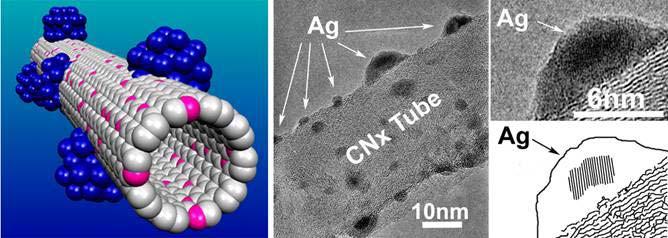
PHYS-E0541:Special Course in Physics Gas phase synthesis of carbon nanotubes for thin film application. Electron Microscopy. for
 PHYS-E0541:Special Course in Physics Gas phase synthesis of carbon nanotubes for thin film application Electron Microscopy for Introduction to Electron Microscopy Carbon Nanomaterials (nanotubes) Dr. Hua
Chapter 9. Electron mean free path Microscopy principles of SEM, TEM, LEEM
 Chapter 9 Electron mean free path Microscopy principles of SEM, TEM, LEEM 9.1 Electron Mean Free Path 9. Scanning Electron Microscopy (SEM) -SEM design; Secondary electron imaging; Backscattered electron
n The visual examination of the image of a point source is one of the most basic and important tests that can be performed.
 8.2.11 Star Test n The visual examination of the image of a point source is one of the most basic and important tests that can be performed. Interpretation of the image is to a large degree a matter of
Lecture 9: Introduction to Diffraction of Light
 Lecture 9: Introduction to Diffraction of Light Lecture aims to explain: 1. Diffraction of waves in everyday life and applications 2. Interference of two one dimensional electromagnetic waves 3. Typical
CHARACTERIZATION of NANOMATERIALS KHP
 CHARACTERIZATION of NANOMATERIALS Overview of the most common nanocharacterization techniques MAIN CHARACTERIZATION TECHNIQUES: 1.Transmission Electron Microscope (TEM) 2. Scanning Electron Microscope
Elastic and Inelastic Scattering in Electron Diffraction and Imaging
 Elastic and Inelastic Scattering in Electron Diffraction and Imaging Contents Introduction Symbols and definitions Part A Diffraction and imaging of elastically scattered electrons Chapter 1. Basic kinematical
Aberration-corrected TEM studies on interface of multilayered-perovskite systems
 Aberration-corrected TEM studies on interface of multilayered-perovskite systems By Lina Gunawan (0326114) Supervisor: Dr. Gianluigi Botton November 1, 2006 MSE 702(1) Presentation Outline Literature Review
November 30th -December 2 nd, st 2nd 3rd. 8:15 7)HRTEM 10) TEM imaging and diffraction examples. 9:15 8)HRTEM 10) Diffraction going further
HRTEM 10) TEM imaging and diffraction examples. 9:15 8)HRTEM 10) Diffraction going further") Thomas LaGrange, Ph.D. Faculty and Staff Scientist Introduction: Basics of Transmission Electron Microscopy (TEM) TEM Doctoral Course MS-637 November 30th -December 2 nd, 2015 Planning MSE-637 TEM -basics
Thomas LaGrange, Ph.D. Faculty and Staff Scientist Introduction: Basics of Transmission Electron Microscopy (TEM) TEM Doctoral Course MS-637 November 30th -December 2 nd, 2015 Planning MSE-637 TEM -basics
Interference, Diffraction and Fourier Theory. ATI 2014 Lecture 02! Keller and Kenworthy
 Interference, Diffraction and Fourier Theory ATI 2014 Lecture 02! Keller and Kenworthy The three major branches of optics Geometrical Optics Light travels as straight rays Physical Optics Light can be
The Principles of STEM Imaging
 2 The Principles of STEM Imaging Peter D. Nellist 2.1 Introduction The purpose of this chapter is to review the principles underlying imaging in the scanning transmission electron microscope (STEM). Consideration
NANO 703-Notes. Chapter 21: Using CBED
 1 Chapter 21: Using CBED CBED features Common features in a CBED pattern can be seen in the example below. Excess and defect ZOLZ Kikuchi lines are fairly strong and broad. (Defect) HOLZ (Bragg) lines
Light Propagation in Free Space
 Intro Light Propagation in Free Space Helmholtz Equation 1-D Propagation Plane waves Plane wave propagation Light Propagation in Free Space 3-D Propagation Spherical Waves Huygen s Principle Each point
Supplementary Information
 Supplementary Information Supplementary Figures Supplementary figure S1: Characterisation of the electron beam intensity profile. (a) A 3D plot of beam intensity (grey value) with position, (b) the beam
Supplementary Information
 Supplementary Information Direct observation of crystal defects in an organic molecular crystals of copper hexachlorophthalocyanine by STEM-EELS Mitsutaka Haruta*, Hiroki Kurata Institute for hemical Research,
CHEM-E5225 :Electron Microscopy. Diffraction 1
 CHEM-E5225 :Electron Microscopy Diffraction 1 2018-10-15 Yanling Ge Text book: Transmission electron microscopy by David B Williams & C. Barry Carter. 2009, Springer Outline Diffraction in TEM Thinking
Structure analysis: Electron diffraction LEED TEM RHEED
 Structure analysis: Electron diffraction LEED: Low Energy Electron Diffraction SPA-LEED: Spot Profile Analysis Low Energy Electron diffraction RHEED: Reflection High Energy Electron Diffraction TEM: Transmission
31. Diffraction: a few important illustrations
 31. Diffraction: a few important illustrations Babinet s Principle Diffraction gratings X-ray diffraction: Bragg scattering and crystal structures A lens transforms a Fresnel diffraction problem into a
These authors contributed equally to this work. 1. Structural analysis of as-deposited PbS quantum dots by Atomic Layer Deposition (ALD)
") Supporting information for: Atomic Layer Deposition of Lead Sulfide Quantum Dots on Nanowire Surfaces Neil P. Dasgupta 1,*,, Hee Joon Jung 2,, Orlando Trejo 1, Matthew T. McDowell 2, Aaron Hryciw 3, Mark
Supporting information for: Atomic Layer Deposition of Lead Sulfide Quantum Dots on Nanowire Surfaces Neil P. Dasgupta 1,*,, Hee Joon Jung 2,, Orlando Trejo 1, Matthew T. McDowell 2, Aaron Hryciw 3, Mark
Design and Correction of optical Systems
 Design and Correction of optical Systems Part 10: Performance criteria 1 Summer term 01 Herbert Gross Overview 1. Basics 01-04-18. Materials 01-04-5 3. Components 01-05-0 4. Paraxial optics 01-05-09 5.
X-Ray Diffraction as a key to the Structure of Materials Interpretation of scattering patterns in real and reciprocal space
 X-Ray Diffraction as a key to the Structure of Materials Interpretation of scattering patterns in real and reciprocal space Tobias U. Schülli, X-ray nanoprobe group ESRF OUTLINE 1 Internal structure of
Oak Ridge, Tennessee, , USA. 2 Nanoscale Physics Research Laboratory, School of Physics and
 Z-CONTRAST SCANNING TRANSMISSION ELECTRON MICROSCOPY S. J. PENNYCOOK 1 AND P. D. NELLIST 2 1 Solid State Division, Oak Ridge National Laboratory, Oak Ridge, Tennessee, 37831-6030, USA. 2 Nanoscale Physics
MEMS Metrology. Prof. Tianhong Cui ME 8254
 MEMS Metrology Prof. Tianhong Cui ME 8254 What is metrology? Metrology It is the science of weights and measures Refers primarily to the measurements of length, weight, time, etc. Mensuration- A branch
Microscopy: Principles
 Low Voltage Electron Microscopy: Principles and Applications Edited by David C. Bell Harvard University, USA and Natasha Erdman JEOL USA Inc., USA Published in association with the Royal Microscopical
Physics I : Oscillations and Waves Prof. S. Bharadwaj Department of Physics and Meteorology Indian Institute of Technology, Kharagpur
 Physics I : Oscillations and Waves Prof. S. Bharadwaj Department of Physics and Meteorology Indian Institute of Technology, Kharagpur Lecture - 21 Diffraction-II Good morning. In the last class, we had
Electron microscopy in molecular cell biology I
 Electron microscopy in molecular cell biology I Electron optics and image formation Werner Kühlbrandt Max Planck Institute of Biophysics chemistry biology Objects of interest Galaxy 10 6 light years 10
QUANTUM PHYSICS. Limitation: This law holds well only for the short wavelength and not for the longer wavelength. Raleigh Jean s Law:
 Black body: A perfect black body is one which absorbs all the radiation of heat falling on it and emits all the radiation when heated in an isothermal enclosure. The heat radiation emitted by the black
Transmission Electron Microscopy. Part #2 High Resolution Imaging XEDS EELS spectroscopies Aberration corrected TEM
 Transmission Electron Microscopy Part #2 High Resolution Imaging XEDS EELS spectroscopies Aberration corrected TEM Nicolas Menguy Institut de Minéralogie, de Physique des Matériaux et de Cosmochimie Part
Controllable Atomic Scale Patterning of Freestanding Monolayer. Graphene at Elevated Temperature
 Controllable Atomic Scale Patterning of Freestanding Monolayer Graphene at Elevated Temperature AUTHOR NAMES Qiang Xu 1, Meng-Yue Wu 1, Grégory F. Schneider 1, Lothar Houben 2, Sairam K. Malladi 1, Cees
Physical Principles of Electron Microscopy. 2. Electron Optics
 Physical Principles of Electron Microscopy 2. Electron Optics Ray Egerton University of Alberta and National Institute of Nanotechnology Edmonton, Canada www.tem-eels.ca regerton@ualberta.ca Properties
Chapter 6 SCALAR DIFFRACTION THEORY
 Chapter 6 SCALAR DIFFRACTION THEORY [Reading assignment: Hect 0..4-0..6,0..8,.3.3] Scalar Electromagnetic theory: monochromatic wave P : position t : time : optical frequency u(p, t) represents the E or
gives rise to multitude of four-wave-mixing phenomena which are of great
 Module 4 : Third order nonlinear optical processes Lecture 26 : Third-order nonlinearity measurement techniques: Z-Scan Objectives In this lecture you will learn the following Theory of Z-scan technique
Atomic Resolved HAADF-STEM for Composition Analysis
 Volume 38 Number 2 November 10, 2003 Atomic Resolved HAADF-STEM for Composition Analysis Makoto Shiojiri,, and Takashi. Yamazaki Kanazawa Medical University, Ishikawa 920-0293, Japan Kyoto Institute of
Electron-Matter Interactions
 Electron-Matter Interactions examples of typical EM studies properties of electrons elastic electron-matter interactions scattering processes; coherent and incoherent image formation; chemical contrast;
Nanoelectronics 09. Atsufumi Hirohata Department of Electronics. Quick Review over the Last Lecture
 Nanoelectronics 09 Atsufumi Hirohata Department of Electronics 13:00 Monday, 12/February/2018 (P/T 006) Quick Review over the Last Lecture ( Field effect transistor (FET) ): ( Drain ) current increases
Optical/IR Observational Astronomy Telescopes I: Telescope Basics. David Buckley, SAAO
 David Buckley, SAAO 27 Feb 2012 1 Some other Telescope Parameters 1. Plate Scale This defines the scale of an image at the telescopes focal surface For a focal plane, with no distortion, this is just related
Nature of Light Part 2
 Nature of Light Part 2 Fresnel Coefficients From Helmholts equation see imaging conditions for Single lens 4F system Diffraction ranges Rayleigh Range Diffraction limited resolution Interference Newton
Nano-optics. Topics: How do we image things on the nanoscale? How do we use nanofabrication for new optical devices? COSMOS 2006 Lecture 1
 Nano-optics Topics: How do we image things on the nanoscale? How do we use nanofabrication for new optical devices? Wave Optics 1. Electromagnetic wave x Ex λ Direction of Propagation y z z plane wave
Engineering Physics 1 Prof. G.D. Vermaa Department of Physics Indian Institute of Technology-Roorkee
 Engineering Physics 1 Prof. G.D. Vermaa Department of Physics Indian Institute of Technology-Roorkee Module-04 Lecture-02 Diffraction Part - 02 In the previous lecture I discussed single slit and double
Lithium Atom Microscopy at Sub-50pm Resolution by R005
 Volume 45 Number 1 July, 2010 Lithium Atom Microscopy at Sub-50pm Resolution by R005 Contents Lithium Atom Microscopy at Sub-50pm Resolution by R005............... 2 Atomic-Resolution Elemental Mapping
Ecole Franco-Roumaine : Magnétisme des systèmes nanoscopiques et structures hybrides - Brasov, Modern Analytical Microscopic Tools
 1. Introduction Solid Surfaces Analysis Group, Institute of Physics, Chemnitz University of Technology, Germany 2. Limitations of Conventional Optical Microscopy 3. Electron Microscopies Transmission Electron
Chapter 10. Interference of Light
 Chapter 10. Interference of Light Last Lecture Wave equations Maxwell equations and EM waves Superposition of waves This Lecture Two-Beam Interference Young s Double Slit Experiment Virtual Sources Newton
Image Assessment San Diego, November 2005
 Image Assessment San Diego, November 005 Pawel A. Penczek The University of Texas Houston Medical School Department of Biochemistry and Molecular Biology 6431 Fannin, MSB6.18, Houston, TX 77030, USA phone:
Lecture 20 Optical Characterization 2
 Lecture 20 Optical Characterization 2 Schroder: Chapters 2, 7, 10 1/68 Announcements Homework 5/6: Is online now. Due Wednesday May 30th at 10:00am. I will return it the following Wednesday (6 th June).
2.71. Final examination. 3 hours (9am 12 noon) Total pages: 7 (seven) PLEASE DO NOT TURN OVER UNTIL EXAM STARTS PLEASE RETURN THIS BOOKLET
 Total pages: 7 (seven) PLEASE DO NOT TURN OVER UNTIL EXAM STARTS PLEASE RETURN THIS BOOKLET") 2.71 Final examination 3 hours (9am 12 noon) Total pages: 7 (seven) PLEASE DO NOT TURN OVER UNTIL EXAM STARTS Name: PLEASE RETURN THIS BOOKLET WITH YOUR SOLUTION SHEET(S) MASSACHUSETTS INSTITUTE OF TECHNOLOGY
2.71 Final examination 3 hours (9am 12 noon) Total pages: 7 (seven) PLEASE DO NOT TURN OVER UNTIL EXAM STARTS Name: PLEASE RETURN THIS BOOKLET WITH YOUR SOLUTION SHEET(S) MASSACHUSETTS INSTITUTE OF TECHNOLOGY
Chapter 2 Instrumentation for Analytical Electron Microscopy Lecture 5. Chapter 2 CHEM 793, 2011 Fall 1
 Chater Instrumentation for Analytical Electron Microscoy Lecture 5 Chater CHEM 793, 011 Fall 1 Outline Electron Sources (Electron Guns) Thermionic: LaB 6 or W Field emission gun: cold or Schottky Lenses
Introduction to Crystallography and Electron Diffraction
 Introduction to Crystallography and Electron Diffraction Marc De Graef Carnegie Mellon University Sunday July 24, 2016 M&M Conference, July 24-28, 2016, Columbus, OH Overview Introductory remarks Basic
Waves Part III Electromagnetic waves
 Waves Part III Electromagnetic waves Electromagnetic (light) waves Transverse waves Transport energy (and momentum) Can travel through vacuum (!) and certain solids, liquids and gases Do not transport
MS482 Materials Characterization ( 재료분석 ) Lecture Note 5: RBS. Byungha Shin Dept. of MSE, KAIST
 Lecture Note 5: RBS. Byungha Shin Dept. of MSE, KAIST") 2015 Fall Semester MS482 Materials Characterization ( 재료분석 ) Lecture Note 5: RBS Byungha Shin Dept. of MSE, KAIST 1 Course Information Syllabus 1. Overview of various characterization techniques (1 lecture)
2015 Fall Semester MS482 Materials Characterization ( 재료분석 ) Lecture Note 5: RBS Byungha Shin Dept. of MSE, KAIST 1 Course Information Syllabus 1. Overview of various characterization techniques (1 lecture)
Transmission Electron Microscopy for metrology and characterization of semiconductor devices
 Transmission Electron Microscopy for metrology and characterization of semiconductor devices Bert Freitag, Laurens Kwakman, Ivan Lazic and Frank de Jong FEI / ThermoFisher Scientific, Achtseweg Noord 5,
MSE 321 Structural Characterization
 Auger Spectroscopy Auger Electron Spectroscopy (AES) Scanning Auger Microscopy (SAM) Incident Electron Ejected Electron Auger Electron Initial State Intermediate State Final State Physical Electronics
Chapter 12. Nanometrology. Oxford University Press All rights reserved.
 Chapter 12 Nanometrology Introduction Nanometrology is the science of measurement at the nanoscale level. Figure illustrates where nanoscale stands in relation to a meter and sub divisions of meter. Nanometrology
Lecture 6. What is contrast? Eyes: < 5% - can t detect <10% - difficult Enhance digital image electronically I I C I
 Phae Contrat Lecture 6 Scattering/Amplitude Contrat BF/DF: thickne, tilt Low-medium magnification Application Crytal defect: dilocation, tacking fault, phae boundarie, precipitate, defect cluter Contrat:
Resolution of coherent and incoherent imaging systems reconsidered - Classical criteria and a statistical alternative
 Resolution of coherent and incoherent imaging systems reconsidered - Classical criteria and a statistical alternative Sandra Van Aert and Dirk Van Dyck University of Antwerp, Department of Physics, Groenenborgerlaan
Optics.
 Optics www.optics.rochester.edu/classes/opt100/opt100page.html Course outline Light is a Ray (Geometrical Optics) 1. Nature of light 2. Production and measurement of light 3. Geometrical optics 4. Matrix