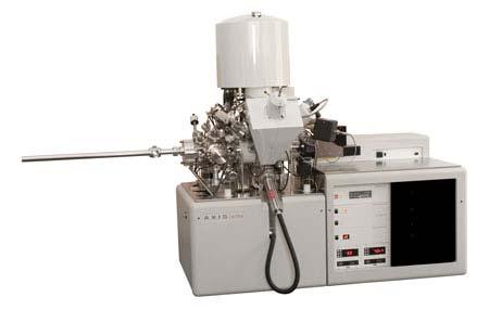
Analytical Methods for Materials
|
|
|
- Sybil Short
- 5 years ago
- Views:
Transcription
 pp. 16-213. Brandon and Kaplan, Chapter 5, pp.261-331; Chapter 6, pp.")
1 Analytical Methods for Materials Lesson 21 Electron Microscopy and X-ray Spectroscopy Suggested Reading Leng, Chapter 3, pp ; Chapter 4, pp ; Chapter 6, pp P.J. Goodhew, J. Humphreys and R. Beanland, Electron Microscopy and Analysis, 3 rd Edition, (CRC Press, 2001) pp Brandon and Kaplan, Chapter 5, pp ; Chapter 6, pp
2 About these notes This is a very long module. This particular set of lecture notes represents an abbreviated introduction to electron microscopy. For the student, this set of notes only scratches the surface. You are still responsible for the majority of chapters 3, 4, and 6 in your text. 858
3 What are electron microscopes? Scientific instruments that use a focused beam of electrons to examine objects with much higher magnification and resolution. 859
4 What is electron microscopy? Electron microscopy is the science and technology of using an electron beam to form a magnified image. Advantages: The use of electrons rather than light provides a ~1000 increase in resolving power (i.e., ability to focus fine details) over light. Disadvantages: High cost Time commitment Small areas of analysis 860
5 Magnification and Resolution Magnification = how large an object can be made (and still resolved). image size magnification= object size Resolution = the closest distance between two points that can clearly be resolved as separate entities through the microscope. d r o 2 sin NA = wavelength of illuminant = semi-angle μ = index of refraction NA = numerical aperture 861
6 Advantages of electron microscopy over optical microscopy Higher magnifications in electron microscopes than you can in light microscopes. Smaller wavelengths of radiation leads to higher resolving power. 862
7 Depth of Field How much of the object that we are looking at remains in focus at the same time. DOF is a function of magnification,, and probe size BEAM Scan D f 1.22 sin tan DOF Focus plane Region of image in focus Higher DOF with (many) electron microscopy techniques than light. 863
8 What information can we obtain from electron microscopes? Topography Surface features of an object. How it looks. Morphology Size and shape of particles making up object. Composition Relative amount of elements and compounds making up the object. Structure Crystallography. How atoms are arranged in the object Substructure. Defect type and content. 864
9 Primary types of electron microscopes Transmission electron microscope (TEM) Scanning electron microscope (SEM) 865
10 History of electron microscopes Developed due to limitations of light microscopes LOM: ~1000x magnification; 0.2 m (200 nm) resolution TEM was developed first. M. Knoll and E. Ruska, 1931 Patterned exactly like a LOM. Uses electrons rather than light. SEM came later
11 How the major types of electron microscopes compare Uses FEATURE Source of Illumination Optical Microscope SEM TEM Surface morphology and sections (1-40 m) Surface morphology Sections ( nm) or small particles on thin membranes Visible light High-speed electrons High-speed electrons Best resolution ~200 nm 3 6 nm 0.2 nm Magnification range 2 2, , ,000,000 Depth of field nm mm mm (NA=1.5) (NA=10-3 ) Lens type Glass Electromagnetic Electromagnetic Image rayformation spot On eye by lens On CRT by scanning device On phosphorescent screen by lens Information generated Phases Reflectivity Topography Composition Crystal orientation Limiting Factors Wavelength of light Brightness, signal/noise ratio, emission volume Crystal structure Crystal orientation Defects Composition Lens quality 867


 300 ; (c) and (e) 1400 ; and")
 TEM image and (h) HR-TEM image.")


12 SEM micrographs Electron Microscopes versus Optical Microscopes Figure A series of optical, SEM and TEM micrographs of the high temperature superconductor YBa 2 Cu 3 O 7 at increasing magnification. Original magnifications: (a) 70 ; (b) and (d) 300 ; (c) and (e) 1400 ; and (f) (g) TEM image and (h) HR-TEM image. Images (a) (f) reproduced from Goodhew, Humphreys & Beanland, Electron Microscopy and Microanalysis, 3 rd Edition, Taylor & Francis, London, Images (g) and (h) reproduced from V. F. Solovyov et al., Superconductor Science and Technology 20 (2007) pp. L20 L23. TEM micrograph HRTEM micrograph LOM micrographs 868
13 How do electron microscopes work? Form a stream of electrons and accelerate them towards a specimen using a positive electrical potential. Use apertures and magnetic lenses to focus the stream onto the sample. Interactions occur inside the irradiated area of the sample that we collect in a suitable detector. 869
14 Thermionic Illumination sources (aka, electron guns) Tungsten LaB 6 Field Emission Cold FEG Schottky FEG 870
15 (From Leng, p. 82) 871
16 Anatomy of an electron source (i.e., electron gun) 2 WEHNELT ELECTRODE (negative potential) Space charge 3 ANODE PLATE (positive potential) Electron Beam 1 CATHODE (negative potential) Crossover kv + Bias resistor Ground 872
17 Electron Lenses Use electrostatic or electromagnetic fields to focus beams of charged electrons. ELECTROMAGNETIC Most lenses are of this type. Consist of Cu wire coils around soft Fe cores. Sometimes an Fe pole-piece is used to shape the field. ELECTROSTATIC Unusual. Only common example is the Wehnelt aperture in the electron gun. 873
18 Electromagnetic Lenses Soft Fe pole pieces Electron beam Consists of a soft magnetic core (case) that encloses a solenoid. N S N S Poles located at annular opening in case. Focus Cu coils Concentrates magnetic field between poles. Figure 3.3 Structure of an electromagnetic lens. The magnetic field concentrated between the N and S poles deflects the electron beam. Adapted from Leng, p
19 Electron Lenses OPTICAL LENS Light Source ELECTROMAGNETIC lenses focus the electron beam to as small a spot as is possible. They are equivalent to convex lenses in optical lens systems. Soft Fe pole pieces MAGNETIC LENS Cu coils Electron Source N S N S 875
20 Imaging System (lenses) We use combinations of electromagnetic lenses to increase magnification. Electron gun 0.02 mm Image from objective lens ( 50) Vacuum column + Tilt & rotation z x y Intermediate lens ( 20) 0.4 mm Projector lens 1 ( 20) 8 mm Projector lens 2 ( 25) Phosphor screen; film; digital recording system 1 in electrons are collected 200 mm Final image Final magnification = = 500,000 Adapted from B.D. Huey, MMAT322 Lecture Notes, University of Connecticut (2005) AND 876
21 Electrons in Magnetic Fields A. Electrons moving through a perpendicular magnetic field experience perpendicular forces. B. Electrons moving parallel to a magnetic field are unaffected. C. Electrons moving nearly parallel to a magnetic field adopt a helical path around the direction of the magnetic field. A B C electron Force on electron is out of plane Magnetic field Nearly aligned electron unaffected No Force Electrons follow a helical path Adapted from B.D. Huey, MMAT322 Lecture Notes, University of Connecticut (2005) 877
22 Trajectories in Electromagnetic Lenses When you adjust the magnification (and the focal length), you modify the lens strength by adjusting the current in the electromagnetic lens coils. Since the magnetic field is changed, MAGNETIC LENS so are the helical trajectories. Leads to image rotation in TEM (which must be corrected for or calibrated on older microscopes). Soft Fe pole pieces Electron Source N N S S Object Cu coils Rotated image Image is inverted and rotated 878
23 Apertures Similar to light microscopes Essentially a piece of metal with a hole in it. Used to limit scattering and/or to select the diffracted or non-diffracted beams. (From Leng) 879
24 Types of Apertures Objective Condenser Selected area Each has a specific function 880
25 WHAT HAPPENS WHEN ELECTRONS INTERACT WITH A MATERIAL? 881
26 Interaction Volume Represents the region penetrated by electrons. Surface of specimen Incident electrons Auger electrons Secondary electrons Backscattered electrons Continuum X-ray emission Fluorescent X-ray emission Characteristic X-ray emission Absorbed electrons 882
27 Signals originate from different depths inside of the sample Signals must escape the sample to be detected INCIDENT BEAM ~50 nm TEM specimen thickness ~300 nm Backscattered electrons ~5 50 nm Secondary electrons ~1 nm Auger electrons ~1.5 m X-rays ~1.0 m X-ray resolution Z = 29 (Cu), Accelerating voltage = 20kV 883
28 Signals and Electron Microscopy Incident high kv beam of electrons Backscattered e - (BSE) Secondary e - (SE) Characteristic x-rays Bulk (SEM) Foil (TEM) Auger e - Absorbed e - e - - hole pairs Visible light Bremsstrahlung x-rays (noise) Interaction Volume Elastically scattered e - Direct (transmitted) beam Inelastically scattered e - Important signals in analytical electron microscopy X-rays Backscattered electrons Secondary electrons 884
29 Backscattered electrons (BSE) Formation Caused when incident electrons collide with an atom in a specimen that is nearly normal to the path of the incident beam. Incident electron is scattered backward ( reflected ). Use Imaging and diffraction analysis in the SEM. Production varies with atomic number (Z). Higher Z elements appear brighter than lower Z elements. Differentiate parts of specimen having different atomic number Backscattered electrons are not as numerous as others. However, they generally carry higher energies than other types of electrons. 885
30 Formation Use Secondary Electrons (SE) Caused when an incident electron knocks and inner shell electron (e.g., k-shell) out of its site. This causes a slight energy loss and path change in the incident electron and ionization of the electron in the specimen. The ionized electron leaves the atom with a small kinetic energy (~5 ev) IMAGING! Production is related to topography. Due to low energy, only SE near the surface can exit the sample. Any change in topography that is larger than the sampling depth will change the yield of SE. More abundant than other types of electrons. They are electrons that escape the specimen with energies below ~50eV 886
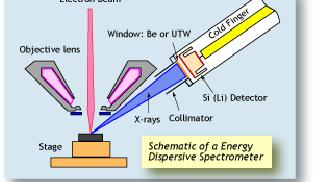
31 X-rays Formation Same as AE. Difference is that the electron that fills the inner shell emits energy to balance the total energy of the atom. Use X-rays will have characteristic energies that are unique to the element(s) from which it originated. Collect and sort signals according to energy or wavelength to yield compositional information. Energy Dispersive X-ray Spectroscopy (EDS) Wavelength Dispersive X-ray Spectroscopy (WDS) Also foundation of XPS (X-ray photoelectron spectroscopy). XPS can be used to determine the state of an atom and to identify chemical compounds. 887
32 Transmitted electrons Used in Transmission Electron Microscopy (TEM) Can be used to determine: thickness crystallographic orientation atomic arrangements phases present etc. 888
33 Formation Auger Electrons (AE) De-energizing of the atom after a secondary electron is produced. During SE production, an inner shell electron is emitted from the atom leaving a vacancy. Higher energy electrons from the same atom can fall into the lower energy hole. This creates an energy surplus in the atom which is corrected by emission of an outer shell (low energy) electron. Use AE have characteristic energies that are unique to each element from which they are emitted. Collect and sort AE according to energy to determine composition. AE have very low energy and are emitted from near surface regions. SURFACE SCIENCE! 889
34 Size of specimen Interaction Volume Depends upon: Z of material being examined higher Z materials absorb more electrons and have smaller interaction volume Accelerating Voltage higher voltages penetrate further into the specimen and generate larger interaction volumes Angle of incidence of electron beam larger angle leads to a smaller interaction volume 890
35 Effects of accelerating voltage and Z on interaction volume Increasing incident energy (E 0 ) ~50 nm Z 1 Z 2 Z 3 < Z 2 < Z 1 Z 3 Increasing atomic number (Z) Interaction volume is larger for materials that have lower atomic numbers and for higher incident beam energies! 891
36 Instruments of the trade Primary Instruments Transmission Electron Microscope (TEM) Scanning Electron Microscope (SEM) Variants Electron Probe Microanalyzer (EPMA); i.e., microprobe Scanning Transmission Electron Microscope (STEM) Environmental SEM (ESEM) {aka variable pressure SEM} High Resolution TEM (HRTEM) High Voltage TEM (HVTEM) DualBeam FIB etc... There are others as well. All have specific purposes. 892


37 TEM SEM EPMA Tabletop SEM 893


38 XPS / ESCA DB-FIB He-Ion Microscope 894
39 LET S CONSIDER THE TEM FOLLOWED BY THE SEM 895
40 TEM Patterned after transmission optical microscopes Yield Following Information: Morphology Size shape and arrangement of particles, precipitates, etc. Crystallographic information Atomic arrangement Compositional Information If proper detector is present 896


41 TEM is a projection device From the lecture notes of Hendrik O. Colijn, OSU Campus Electron Optics Facility, 897
42 Similarity of LM and TEM From the lecture notes of Hendrik O. Colijn, OSU Campus Electron Optics Facility, 898
43 Similarity of LM and TEM From the lecture notes of Hendrik O. Colijn, OSU Campus Electron Optics Facility, 899
44 Components of the TEM Electron gun Source filament plus anode plates with applied accelerating voltage. Vacuum column + Tilt & rotation z x y Condenser Lenses electromagnetic lenses adjusted by lens currents not position. Specimen Stage allows translations and tilts. Objective Lens usually <50X. Imaging System multiple electromagnetic lenses below the objective: set magnification, focal plane (image vs. diffraction pattern). Phosphor screen; film; digital recording system 1 in electrons are collected Detector/Imaging fluorescent screen, plate film, CCD camera. Instruments often have attachments such as X-ray detectors 900


45 From the lecture notes of Hendrik O. Colijn, OSU Campus Electron Optics Facility, TEM Schematic 901
46 How does a TEM work? Pass a focused beam of electrons through a thin foil As beam passes through sample, it is scattered Project the transmitted (scattered) beam onto a phosphor screen to form an enlarged image. Imaging Modes: Bright Field / Dark Field modes for visualization of structure and defects Selected Area Diffraction / Convergent Beam Diffraction for crystallographic information 902
47 Contrast in TEM Generated when there is a difference in the number of electrons being scattered away from the transmitted beam. Mechanisms: Mass-density contrast Diffraction contrast 903

48 Mass-density Contrast Difference in thickness and density in specimen generates variation in electron intensity. (Figures from Leng) 904

49 When Bragg s law is satisfied, constructive diffraction occurs resulting in reduced intensity of the transmitted beam. Diffraction Contrast (Figures (a) and (b) from Leng) 905
50 TEM Imaging In most cases, you are using amplitude contrast rather than phase contrast. Like light microscopy, you can do BF and DF imaging. You can also do diffraction from submicron areas to examine crystal structure. Adapted from the lecture notes of Hendrik O. Colijn, OSU Campus Electron Optics Facility,

51 Brightfield vs. Darkfield Specimen Obj. aperture (Figures from Leng) 907


52 Phase Contrast Provides highest resolution of lattice. Used primarily in HRTEM. (Figures from Leng) 908
53 Diffraction vs. Imaging Diffraction Modes: intermediate lens focused on backfocal plane plane of objective lens (where diffraction pattern forms). Imaging Modes: intermediate lens focused on image plane of objective lens. stronger lens - shorter focal length Adapted from the lecture notes of Hendrik O. Colijn, OSU Campus Electron Optics Facility, 909
54 Selected Area Diffraction Specimen Obj. aperture Phase ID Crystal orientation (Figures from Leng) 910
55 Beam Tilting and Translation The electron beam can be positioned for fine measurements (spot modes) or scanning (SEM, STEM) BEAM TILTING APPARENT ORIGIN BEAM TRANSLATION APPARENT ORIGIN Upper scan coil Lower scan coil 911


56 Scanning TEM (STEM) Selection of bright field or dark field electrons results in contrast variations that provide crystallographic information. Scanning beam Scanning beam Specimen Specimen BF DF DF BF selected DF selected Adapted from MATTER website ( 912
57 More on TEM There are plenty of things that we can do with a TEM that go far beyond the scope of this introductory course. Phase identification Defect identification and analysis Etc Some of them are described in Ch. 3 of the text. You can learn about these things in MTE 655 (Transmission Electron Microscopy). 913
 C2 changes intensity or brightness Use condenser aperture to restrict the beam Part of the beam is transmitted through the sample Focus transmitted portion using the objective lens to form an")
58 Some Technical Details Produce a stream of monochromatic electrons in the electron gun Focus the stream into a small coherent beam using C1 and C2 C1 determines the spot size (i.e., size of electron probe) C2 changes intensity or brightness Use condenser aperture to restrict the beam Part of the beam is transmitted through the sample Focus transmitted portion using the objective lens to form an image Objective and selected area apertures are used to restrict the beam further allows examination of diffraction from specific atoms, crystals, features SAD, CBD Enlarge image with intermediate and projector lenses 914
59 SEM Patterned after reflecting light optical microscopes Forms an image by scanning a focused beam of electrons over the surface of a sample Yield Following Information: Topography Surface features of an object. Detectable features limited to a few nanometers depth. Morphology Size shape and arrangement of particles, precipitates, etc Compositional Information Elements and compounds the sample is composed of Crystallographic information Possible using new techniques (OIM/BKD)a 915
60 SEM Adapted from the lecture notes of Hendrik O. Colijn, OSU Campus Electron Optics Facility, 916
61 TEM SEM Electron gun Electron gun Vacuum column Also tilts and rotates z Condenser system y Stage x Condenser lens Scan coils Time base Objective lens Probe lens Final imaging system z y Stage Signal amplifier x Observation and recording system Also tilts and rotates Detector and processing system CRT In the SEM you use secondary signals to acquire images. 917
62 Components of an SEM Source: same as TEM but lower V Condenser: same as TEM Scan Coils: raster the probe Probe Lens: lens that forms a spot at the specimen surface Detector & Processing System: collects signals such as X-rays and electrons as a function of time and position. Provides digital images for real-time viewing, processing, and storage. z x y Also tilts and rotates Electron gun Condenser lens Scan coils Probe lens Stage Time base Detector and processing system Signal amplifier CRT 918
63 Structure of SEM Two condensers used to reduce crossover diameter of e-beam Objective focuses e-beam (Figures from Leng) 919
")
64 B.D. Huey, MMAT322 Lecture Notes, University of Connecticut (2005) 920

65 Comparison of LM and SEM images LOM SEM Increased DOF! Z contrast! (Figures from Leng) 921
66 SEM: Technical Details Produce a stream of monochromatic electrons in the electron gun Focus the stream using the first condenser lens Coarse probe current knob The beam is constricted by the condenser aperture (eliminates high-angle electrons) Second condenser lens is used to form electrons into a thin, tight, coherent beam. Use fine probe current knob Use objective aperture to limit beam (i.e., eliminate high-angle electrons) Scan coils raster the beam across the sample, dwelling on the points for a predetermined period of time (selected using scan speed) Final objective lens focuses beam on desired region. When beam strikes the sample, interactions occur. We detect what comes out of the sample. 922
 (b) (Figures from")
67 Secondary electron mode Topographic contrast 200 m Secondary electron detector (a) (b) (Figures from Leng) 923

 p.")
68 You can use BSE signals in conjunction with SE signals to yield enhanced topographical information SE image Multiple elements of BSE detector Overlapping shadows Reduced resolution Single segment of BSE detector P.J. Goodhew, J. Humphreys, and R. Beanland, Electron Microscopy and Analysis, 3 rd edition; (Taylor Francis, London, 2001) p. 144 The BSE sampling volume is large which limits resolution 924

69 Secondary electron mode Topographic contrast Some atomic number contrast 925

70 Secondary vs. Backscattered Higher resolution No Z contrast Lots of Z contrast Lower resolution (Figures reproduced from Leng) 926

71 More backscattering observed for high Z (qualitative chemical sensitivity). Imaging with BSE s Local contrast is higher when sample is normal to the beam. 10 m Local contrast is lower when the sample is tilted away from the beam. Al-Ta-Ti ternary alloy α 2 = (Ti,Ta) 3 Al σ = Al 2 (Ta,Ti) 927

")

72 Electron Backscattered Diffraction Yields crystallographic contrast Principal components of an EBSD system A.W. Wilson and G. Spanos, Materials Characterization, 46 (2001) Photograph of an SEM chamber showing typical arrangement for EBSD Figure 1 Copyright Oxford Instruments PLC

73 As the beam is moved from grain to grain the electron backscatter diffraction pattern (EBSP) will change due to the change in orientation of the crystal lattice in the diffracting volume Adapted from 929


74 A Grain Boundary Map can be generated by comparing the orientation between each pair of neighboring points in an OIM scan. A line is drawn separating a pair of points if the difference in orientation between the points exceeds a given tolerance angle. An Orientation Map is generated by shading each point in the OIM scan according to some parameter reflecting the orientation at each point. Both of these maps are shown overlaid on the digital micrograph from the SEM. Adapted from 930
75 SEM vs. TEM Image formation TEM parallel optics and lenses; SEM focused optics and detectors. Depth of field Small apertures yield high magnifications (i.e., diameter of object >> δ) for both; SEM up to 20 μm thickness and TEM up to 200 nm thickness. Specimens TEM lens and holder geometry limit samples to 3 mm dia. and 150 μm thick. SEM limited by size of chamber. Vacuum system Vacuum required for both. Eliminates scattering of electron beam, contamination of specimen and/or microscope components, and gun instabilities. Better vacuum systems are required for TEM than SEM. 931
76 CHEMICAL ANALYSIS (aka Microanalysis) 932
77 Microanalysis in Electron Microscopy Characteristic X-rays are always generated by interactions between the incident electron beam and the sample. They constitute a fingerprint of the local chemistry. Collect X-ray signal to determine local chemistry. Common spectroscopic techniques: Wavelength-Dispersive Spectrometry/Spectroscopy (WDS) Energy-Dispersive Spectrometry/Spectroscopy (EDS) Micro X-ray Fluorescence (micro XRF) 933
78 EDS vs. WDS WDS EDS (a) (b) Figure 6.6 Main components and dispersive spectra of : (a) WDS; and (b) EDS. (Figures reproduced from Leng) WDS uses single crystal diffraction to detect characteristic wavelengths emitted by specimen EDS uses photon detector to separate characteristic x-ray photons according to energy 934


79 EDS vs. WDS 935
 Figure 4.")
80 Backscattered electron mode and WDS analysis Atomic number contrast Substrate IDZ Coating Substrate Ni-AD Ni-Annealed Al-AD Al-Annealed IDZ + ' Ni Al + + Composition (at%) Pt-AD Pt-Annealed Pt 10 m X-ray detectors are common Allow chemical analysis EDS, WDS, XRF Hf-AD Hf-Annealed Hf Distance ( m) Figure 4.8. Composition profiles of the major elements measured by WDS in an EPMA. 936

 Backscattered image, (b) Si Lα elemental")
 showing the individual pixels.")

81 EDS mapping (b) (c) (a) (f) (d) (e) Figure 6.11 EDS maps of a polished specimen of a hard-facing alloy. (a) Backscattered image, (b) Si Lα elemental map, (c) Mo Kα, (d) Cr Kα, (e) Co Kα, and (f) detail of (e) showing the individual pixels. (Figure adapted from P.J. Goodhew and F.J. Humphreys, Electron Microscopy and Analysis, 3 rd ed., (Taylor & Francis, London, 1988) pp ) 937
82 WDS Yields best discrimination of emitted X-ray signal Use a series of bent crystals to cover the range of wavelengths of interest Scan wavelengths within each range by rotating the crystal and moving the detector while keeping the position of the crystal fixed. X-rays are collected from the sample at a fixed angle. The angle at the collecting crystal will vary with 2 and the diameter of the focusing circle will change 938

83 Comparison of resolution of Mo and S spectral lines in EDS (yellow) vs. WDS (blue). In the EDS spectrum the molybdenum and sulfur lines are overlapped, but can be resolved in the WDS spectrum. Image from Oxford Instruments. 939
84 EDS vs. WDS Pulse height is recorded by the detector. It is related to the energy of the photon responsible for the pulse. Solid-state detectors are generally used. EDS is faster than WDS Problems with EDS: Poor discrimination or energy resolution. WDS systems are much better, particularly when characteristic lines from different elements overlap. Need a windowless or thin window detector to pick up light elements. WDS is more quantitative 940
Electron Microprobe Analysis 1 Nilanjan Chatterjee, Ph.D. Principal Research Scientist
 12.141 Electron Microprobe Analysis 1 Nilanjan Chatterjee, Ph.D. Principal Research Scientist Massachusetts Institute of Technology Electron Microprobe Facility Department of Earth, Atmospheric and Planetary
Electron Microprobe Analysis 1 Nilanjan Chatterjee, Ph.D. Principal Research Scientist
 12.141 Electron Microprobe Analysis 1 Nilanjan Chatterjee, Ph.D. Principal Research Scientist Massachusetts Institute of Technology Electron Microprobe Facility Department of Earth, Atmospheric and Planetary
= 6 (1/ nm) So what is probability of finding electron tunneled into a barrier 3 ev high?
 So what is probability of finding electron tunneled into a barrier 3 ev high?") STM STM With a scanning tunneling microscope, images of surfaces with atomic resolution can be readily obtained. An STM uses quantum tunneling of electrons to map the density of electrons on the surface
STM STM With a scanning tunneling microscope, images of surfaces with atomic resolution can be readily obtained. An STM uses quantum tunneling of electrons to map the density of electrons on the surface
Transmission Electron Microscopy
 L. Reimer H. Kohl Transmission Electron Microscopy Physics of Image Formation Fifth Edition el Springer Contents 1 Introduction... 1 1.1 Transmission Electron Microscopy... 1 1.1.1 Conventional Transmission
MT Electron microscopy Scanning electron microscopy and electron probe microanalysis
 MT-0.6026 Electron microscopy Scanning electron microscopy and electron probe microanalysis Eero Haimi Research Manager Outline 1. Introduction Basics of scanning electron microscopy (SEM) and electron
Scanning Electron Microscopy
 Scanning Electron Microscopy Field emitting tip Grid 2kV 100kV Anode ZEISS SUPRA Variable Pressure FESEM Dr Heath Bagshaw CMA bagshawh@tcd.ie Why use an SEM? Fig 1. Examples of features resolvable using
Chapter 9. Electron mean free path Microscopy principles of SEM, TEM, LEEM
 Chapter 9 Electron mean free path Microscopy principles of SEM, TEM, LEEM 9.1 Electron Mean Free Path 9. Scanning Electron Microscopy (SEM) -SEM design; Secondary electron imaging; Backscattered electron
Why microscopy?
 Electron Microscopy Why microscopy? http://www.cellsalive.com/howbig.htm 2 Microscopes are used as magnifying tools (although not exclusively as will see later on). The resolution of the human eye is limited
AP5301/ Name the major parts of an optical microscope and state their functions.
 Review Problems on Optical Microscopy AP5301/8301-2015 1. Name the major parts of an optical microscope and state their functions. 2. Compare the focal lengths of two glass converging lenses, one with
object objective lens eyepiece lens
 Advancing Physics G495 June 2015 SET #1 ANSWERS Field and Particle Pictures Seeing with electrons The compound optical microscope Q1. Before attempting this question it may be helpful to review ray diagram
Electron probe microanalysis - Electron microprobe analysis EPMA (EMPA) What s EPMA all about? What can you learn?
 What s EPMA all about? What can you learn?") Electron probe microanalysis - Electron microprobe analysis EPMA (EMPA) What s EPMA all about? What can you learn? EPMA - what is it? Precise and accurate quantitative chemical analyses of micron-size
Electron probe microanalysis - Electron microprobe analysis EPMA (EMPA) What s EPMA all about? What can you learn? EPMA - what is it? Precise and accurate quantitative chemical analyses of micron-size
Everhart-Thornley detector
 SEI Detector Everhart-Thornley detector Microscope chamber wall Faraday cage Scintillator Electrons in Light pipe Photomultiplier Electrical signal out Screen Quartz window +200 V +10 kv Always contains
EDS User School. Principles of Electron Beam Microanalysis
 EDS User School Principles of Electron Beam Microanalysis Outline 1.) Beam-specimen interactions 2.) EDS spectra: Origin of Bremsstrahlung and characteristic peaks 3.) Moseley s law 4.) Characteristic
Massachusetts Institute of Technology. Dr. Nilanjan Chatterjee
 Massachusetts Institute of Technology Dr. Nilanjan Chatterjee Electron Probe Micro-Analysis (EPMA) Imaging and micrometer-scale chemical compositional analysis of solids Signals produced in The Electron
HOW TO APPROACH SCANNING ELECTRON MICROSCOPY AND ENERGY DISPERSIVE SPECTROSCOPY ANALYSIS. SCSAM Short Course Amir Avishai
 HOW TO APPROACH SCANNING ELECTRON MICROSCOPY AND ENERGY DISPERSIVE SPECTROSCOPY ANALYSIS SCSAM Short Course Amir Avishai RESEARCH QUESTIONS Sea Shell Cast Iron EDS+SE Fe Cr C Objective Ability to ask the
CHARACTERIZATION of NANOMATERIALS KHP
 CHARACTERIZATION of NANOMATERIALS Overview of the most common nanocharacterization techniques MAIN CHARACTERIZATION TECHNIQUES: 1.Transmission Electron Microscope (TEM) 2. Scanning Electron Microscope
MSE 321 Structural Characterization
 Auger Spectroscopy Auger Electron Spectroscopy (AES) Scanning Auger Microscopy (SAM) Incident Electron Ejected Electron Auger Electron Initial State Intermediate State Final State Physical Electronics
MT Electron microscopy Scanning electron microscopy and electron probe microanalysis
 MT-0.6026 Electron microscopy Scanning electron microscopy and electron probe microanalysis Eero Haimi Research Manager Outline 1. Introduction Basics of scanning electron microscopy (SEM) and electron
Modern Optical Spectroscopy
 Modern Optical Spectroscopy X-Ray Microanalysis Shu-Ping Lin, Ph.D. Institute of Biomedical Engineering E-mail: splin@dragon.nchu.edu.tw Website: http://web.nchu.edu.tw/pweb/users/splin/ Backscattered
Praktikum zur. Materialanalytik
 Praktikum zur Materialanalytik Energy Dispersive X-ray Spectroscopy B513 Stand: 19.10.2016 Contents 1 Introduction... 2 2. Fundamental Physics and Notation... 3 2.1. Alignments of the microscope... 3 2.2.
Weak-Beam Dark-Field Technique
 Basic Idea recall bright-field contrast of dislocations: specimen close to Bragg condition, s î 0 Weak-Beam Dark-Field Technique near the dislocation core, some planes curved to s = 0 ) strong Bragg reflection
h p λ = mν Back to de Broglie and the electron as a wave you will learn more about this Equation in CHEM* 2060
 Back to de Broglie and the electron as a wave λ = mν h = h p you will learn more about this Equation in CHEM* 2060 We will soon see that the energies (speed for now if you like) of the electrons in the
ABC s of Electrochemistry series Materials Characterization techniques: SEM and EDS Ana María Valenzuela-Muñiz November 3, 2011
 ABC s of Electrochemistry series Materials Characterization techniques: SEM and EDS Ana María Valenzuela-Muñiz November 3, 2011 CEER, Department of Chemical and Biomolecular Engineering Outline Introduction
Invited Lecture. "Different Aspects of Electron Microscopy. Sardar Vallabhbhai National Institute of Technology, Surat. Deepak Rajput & S.K.
 Invited Lecture on "Different Aspects of Electron Microscopy at Sardar Vallabhbhai National Institute of Technology, Surat Deepak Rajput & S.K. Tiwary R&D and Product Development Essar Steel Limited Abstract
Basic structure of SEM
 Table of contents Basis structure of SEM SEM imaging modes Comparison of ordinary SEM and FESEM Electron behavior Electron matter interaction o Elastic interaction o Inelastic interaction o Interaction
Part II: Thin Film Characterization
 Part II: Thin Film Characterization General details of thin film characterization instruments 1. Introduction to Thin Film Characterization Techniques 2. Structural characterization: SEM, TEM, AFM, STM
SEM stands for Scanning Electron Microscopy. The earliest known work describing
 1. HISTORY ABOUT SEM SEM stands for Scanning Electron Microscopy. The earliest known work describing the concept of a Scanning Electron Microscope was by M. Knoll (1935) who, along with other pioneers
Gaetano L Episcopo. Scanning Electron Microscopy Focus Ion Beam and. Pulsed Plasma Deposition
 Gaetano L Episcopo Scanning Electron Microscopy Focus Ion Beam and Pulsed Plasma Deposition Hystorical background Scientific discoveries 1897: J. Thomson discovers the electron. 1924: L. de Broglie propose
Practical course in scanning electron microscopy
 Practical course in scanning electron microscopy Fortgeschrittenen Praktikum an der Technischen Universität München Wintersemester 2017/2018 Table of contents 1. Introduction 3 2. Formation of an electron
MSE 321 Structural Characterization
 Optical Microscope Plan Lenses In an "ideal" single-element lens system all planar wave fronts are focused to a point at distance f from the lens; therefore: Image near the optical axis will be in perfect
CBE Science of Engineering Materials. Scanning Electron Microscopy (SEM)
") CBE 30361 Science of Engineering Materials Scanning Electron Microscopy (SEM) Scale of Structure Organization Units: micrometer = 10-6 m = 1µm nanometer= 10-9 m = 1nm Angstrom = 10-10 m = 1Å A hair is
CBE 30361 Science of Engineering Materials Scanning Electron Microscopy (SEM) Scale of Structure Organization Units: micrometer = 10-6 m = 1µm nanometer= 10-9 m = 1nm Angstrom = 10-10 m = 1Å A hair is
QUANTUM PHYSICS. Limitation: This law holds well only for the short wavelength and not for the longer wavelength. Raleigh Jean s Law:
 Black body: A perfect black body is one which absorbs all the radiation of heat falling on it and emits all the radiation when heated in an isothermal enclosure. The heat radiation emitted by the black
PHYS-E0541:Special Course in Physics Gas phase synthesis of carbon nanotubes for thin film application. Electron Microscopy. for
 PHYS-E0541:Special Course in Physics Gas phase synthesis of carbon nanotubes for thin film application Electron Microscopy for Introduction to Electron Microscopy Carbon Nanomaterials (nanotubes) Dr. Hua
SEM Optics and Application to Current Research
 SEM Optics and Application to Current Research Azure Avery May 28, 2008 1 Introduction 1.1 History The optical microscope was invented in the early 17th century. Although revolutionary, the earliest microscopes
Imaging Methods: Scanning Force Microscopy (SFM / AFM)
") Imaging Methods: Scanning Force Microscopy (SFM / AFM) The atomic force microscope (AFM) probes the surface of a sample with a sharp tip, a couple of microns long and often less than 100 Å in diameter.
Imaging Methods: Scanning Force Microscopy (SFM / AFM) The atomic force microscope (AFM) probes the surface of a sample with a sharp tip, a couple of microns long and often less than 100 Å in diameter.
Chemical Analysis in TEM: XEDS, EELS and EFTEM. HRTEM PhD course Lecture 5
 Chemical Analysis in TEM: XEDS, EELS and EFTEM HRTEM PhD course Lecture 5 1 Part IV Subject Chapter Prio x-ray spectrometry 32 1 Spectra and mapping 33 2 Qualitative XEDS 34 1 Quantitative XEDS 35.1-35.4
High-Resolution. Transmission. Electron Microscopy
 Part 4 High-Resolution Transmission Electron Microscopy 186 Significance high-resolution transmission electron microscopy (HRTEM): resolve object details smaller than 1nm (10 9 m) image the interior of
ECE Semiconductor Device and Material Characterization
 ECE 4813 Semiconductor Device and Material Characterization Dr. Alan Doolittle School of Electrical and Computer Engineering Georgia Institute of Technology As with all of these lecture slides, I am indebted
Scanning Electron Microscopy & Ancillary Techniques
 Scanning Electron Microscopy & Ancillary Techniques By Pablo G. Caceres-Valencia The prototype of the first Stereoscan supplied by the Cambridge Instrument Company to the dupont Company, U.S.A. (1965)
MSE 321 Structural Characterization
 Auger Spectroscopy Auger Electron Spectroscopy (AES) Scanning Auger Microscopy (SAM) Incident Electron Ejected Electron Auger Electron Initial State Intermediate State Final State Physical Electronics
MICRO-TOMOGRAPHY AND X-RAY ANALYSIS OF GEOLOGICAL SAMPLES
 THE PUBLISHING HOUSE PROCEEDINGS OF THE ROMANIAN ACADEMY, Series A, OF THE ROMANIAN ACADEMY Volume 18, Number 1/2017, pp. 42 49 MICRO-TOMOGRAPHY AND X-RAY ANALYSIS OF GEOLOGICAL SAMPLES Ion GRUIA University
Electron Microprobe Analysis and Scanning Electron Microscopy
 Electron Microprobe Analysis and Scanning Electron Microscopy Electron microprobe analysis (EMPA) Analytical technique in which a beam of electrons is focused on a sample surface, producing X-rays from
Methods of surface analysis
 Methods of surface analysis Nanomaterials characterisation I RNDr. Věra Vodičková, PhD. Surface of solid matter: last monoatomic layer + absorbed monolayer physical properties are effected (crystal lattice
April 10th-12th, 2017
 Thomas LaGrange, Ph.D. Faculty Lecturer and Senior Staff Scientist Introduction: Basics of Transmission Electron Microscopy (TEM) TEM Doctoral Course MS-637 April 10th-12th, 2017 Outline 1. What is microcopy?
tip conducting surface
 PhysicsAndMathsTutor.com 1 1. The diagram shows the tip of a scanning tunnelling microscope (STM) above a conducting surface. The tip is at a potential of 1.0 V relative to the surface. If the tip is sufficiently
Electron Microscopy I
 Characterization of Catalysts and Surfaces Characterization Techniques in Heterogeneous Catalysis Electron Microscopy I Introduction Properties of electrons Electron-matter interactions and their applications
Nanoelectronics 09. Atsufumi Hirohata Department of Electronics. Quick Review over the Last Lecture
 Nanoelectronics 09 Atsufumi Hirohata Department of Electronics 13:00 Monday, 12/February/2018 (P/T 006) Quick Review over the Last Lecture ( Field effect transistor (FET) ): ( Drain ) current increases
Auger Electron Spectroscopy Overview
 Auger Electron Spectroscopy Overview Also known as: AES, Auger, SAM 1 Auger Electron Spectroscopy E KLL = E K - E L - E L AES Spectra of Cu EdN(E)/dE Auger Electron E N(E) x 5 E KLL Cu MNN Cu LMM E f E
Chapter 10: Wave Properties of Particles
 Chapter 10: Wave Properties of Particles Particles such as electrons may demonstrate wave properties under certain conditions. The electron microscope uses these properties to produce magnified images
Chemistry 311: Instrumentation Analysis Topic 2: Atomic Spectroscopy. Chemistry 311: Instrumentation Analysis Topic 2: Atomic Spectroscopy
 Topic 2b: X-ray Fluorescence Spectrometry Text: Chapter 12 Rouessac (1 week) 4.0 X-ray Fluorescence Download, read and understand EPA method 6010C ICP-OES Winter 2009 Page 1 Atomic X-ray Spectrometry Fundamental
Nano-Microscopy. Lecture 2. Scanning and Transmission Electron Microscopies: Principles. Pavel Zinin HIGP, University of Hawaii, Honolulu, USA
 GG 711: Advanced Techniques in Geophysics and Materials Science Nano-Microscopy. Lecture 2 Scanning and Transmission Electron Microscopies: Principles Pavel Zinin HIGP, University of Hawaii, Honolulu,
CHEM 681 Seminar Mingqi Zhao April 20, 1998 Room 2104, 4:00 p.m. High Resolution Transmission Electron Microscopy: theories and applications
 CHEM 681 Seminar Mingqi Zhao April 20, 1998 Room 2104, 4:00 p.m. High Resolution Transmission Electron Microscopy: theories and applications In materials science, people are always interested in viewing
Lecture 5: Characterization methods
 Lecture 5: Characterization methods X-Ray techniques Single crystal X-Ray Diffration (XRD) Powder XRD Thin film X-Ray Reflection (XRR) Microscopic methods Optical microscopy Electron microscopies (SEM,
Interactions with Matter
 Manetic Lenses Manetic fields can displace electrons Manetic field can be produced by passin an electrical current throuh coils of wire Manetic field strenth can be increased by usin a soft ferromanetic
Electron beam scanning
 Electron beam scanning The Electron beam scanning operates through an electro-optical system which has the task of deflecting the beam Synchronously with cathode ray tube which create the image, beam moves
Auger Electron Spectroscopy (AES) Prof. Paul K. Chu
 Prof. Paul K. Chu") Auger Electron Spectroscopy (AES) Prof. Paul K. Chu Auger Electron Spectroscopy Introduction Principles Instrumentation Qualitative analysis Quantitative analysis Depth profiling Mapping Examples The Auger
Auger Electron Spectroscopy (AES) Prof. Paul K. Chu Auger Electron Spectroscopy Introduction Principles Instrumentation Qualitative analysis Quantitative analysis Depth profiling Mapping Examples The Auger
M2 TP. Low-Energy Electron Diffraction (LEED)
") M2 TP Low-Energy Electron Diffraction (LEED) Guide for report preparation I. Introduction: Elastic scattering or diffraction of electrons is the standard technique in surface science for obtaining structural
M2 TP Low-Energy Electron Diffraction (LEED) Guide for report preparation I. Introduction: Elastic scattering or diffraction of electrons is the standard technique in surface science for obtaining structural
Photoelectron spectroscopy Instrumentation. Nanomaterials characterization 2
 Photoelectron spectroscopy Instrumentation Nanomaterials characterization 2 RNDr. Věra V Vodičkov ková,, PhD. Photoelectron Spectroscopy general scheme Impact of X-ray emitted from source to the sample
6. Analytical Electron Microscopy
 Physical Principles of Electron Microscopy 6. Analytical Electron Microscopy Ray Egerton University of Alberta and National Institute of Nanotechnology Edmonton, Canada www.tem-eels.ca regerton@ualberta.ca
Transmission Electron Microscope. Experimental Instruction
 Transmission Electron Microscope Experimental Instruction In advanced practical course [F-Praktikum] Date: April 2017 Contents 1 Task 3 2 Theoretical Basics 3 2.1 Bragg Diffraction......................................
Surface Sensitivity & Surface Specificity
 Surface Sensitivity & Surface Specificity The problems of sensitivity and detection limits are common to all forms of spectroscopy. In its simplest form, the question of sensitivity boils down to whether
Auger Electron Spectroscopy (AES)
") 1. Introduction Auger Electron Spectroscopy (AES) Silvia Natividad, Gabriel Gonzalez and Arena Holguin Auger Electron Spectroscopy (Auger spectroscopy or AES) was developed in the late 1960's, deriving
1. Introduction Auger Electron Spectroscopy (AES) Silvia Natividad, Gabriel Gonzalez and Arena Holguin Auger Electron Spectroscopy (Auger spectroscopy or AES) was developed in the late 1960's, deriving
CHEM-E5225 :Electron Microscopy X-Ray Spectrometry
 CHEM-E5225 :Electron Microscopy X-Ray Spectrometry 2016.11 Yanling Ge Outline X-ray Spectrometry X-ray Spectra and Images Qualitative and Quantitative X-ray Analysis and Imaging Discussion of homework
Supporting Information s for
 Supporting Information s for # Self-assembling of DNA-templated Au Nanoparticles into Nanowires and their enhanced SERS and Catalytic Applications Subrata Kundu* and M. Jayachandran Electrochemical Materials
Appearance Potential Spectroscopy
 Appearance Potential Spectroscopy Submitted by Sajanlal P. R CY06D009 Sreeprasad T. S CY06D008 Dept. of Chemistry IIT MADRAS February 2006 1 Contents Page number 1. Introduction 3 2. Theory of APS 3 3.
Characterisation of Catalysts Using Secondary and Backscattered Electron In-lens Detectors
 Platinum Metals Rev., 2014, 58, (2), 106 110 FINAL ANALYSIS Characterisation of Catalysts Using Secondary and Backscattered Electron In-lens Detectors Heterogeneous catalysis often involves the use of
Lecture 5. X-ray Photoemission Spectroscopy (XPS)
") Lecture 5 X-ray Photoemission Spectroscopy (XPS) 5. Photoemission Spectroscopy (XPS) 5. Principles 5.2 Interpretation 5.3 Instrumentation 5.4 XPS vs UV Photoelectron Spectroscopy (UPS) 5.5 Auger Electron
Lecture 5 X-ray Photoemission Spectroscopy (XPS) 5. Photoemission Spectroscopy (XPS) 5. Principles 5.2 Interpretation 5.3 Instrumentation 5.4 XPS vs UV Photoelectron Spectroscopy (UPS) 5.5 Auger Electron
Chemistry Instrumental Analysis Lecture 19 Chapter 12. Chem 4631
 Chemistry 4631 Instrumental Analysis Lecture 19 Chapter 12 There are three major techniques used for elemental analysis: Optical spectrometry Mass spectrometry X-ray spectrometry X-ray Techniques include:
4. Inelastic Scattering
 1 4. Inelastic Scattering Some inelastic scattering processes A vast range of inelastic scattering processes can occur during illumination of a specimen with a highenergy electron beam. In principle, many
X-Ray Photoelectron Spectroscopy (XPS)
") X-Ray Photoelectron Spectroscopy (XPS) Louis Scudiero http://www.wsu.edu/~scudiero; 5-2669 Electron Spectroscopy for Chemical Analysis (ESCA) The basic principle of the photoelectric effect was enunciated
X-Ray Photoelectron Spectroscopy (XPS) Louis Scudiero http://www.wsu.edu/~scudiero; 5-2669 Electron Spectroscopy for Chemical Analysis (ESCA) The basic principle of the photoelectric effect was enunciated
UNIT-III QUANTUM PHYSICS
 UNIT-III QUANTUM PHYSICS SYLLABUS Black body radiation Planck s theory (derivation) Deduction of Wien s displacement law and Rayleigh Jeans Law from Planck s theory Compton Effect-Theory and experimental
FXA UNIT G485 Module X-Rays. Candidates should be able to : I = I 0 e -μx
 1 Candidates should be able to : HISTORY Describe the nature of X-rays. Describe in simple terms how X-rays are produced. X-rays were discovered by Wilhelm Röntgen in 1865, when he found that a fluorescent
Chapter Six: X-Rays. 6.1 Discovery of X-rays
 Chapter Six: X-Rays 6.1 Discovery of X-rays In late 1895, a German physicist, W. C. Roentgen was working with a cathode ray tube in his laboratory. He was working with tubes similar to our fluorescent
An Introduction to Diffraction and Scattering. School of Chemistry The University of Sydney
 An Introduction to Diffraction and Scattering Brendan J. Kennedy School of Chemistry The University of Sydney 1) Strong forces 2) Weak forces Types of Forces 3) Electromagnetic forces 4) Gravity Types
MS482 Materials Characterization ( 재료분석 ) Lecture Note 4: XRF
 Lecture Note 4: XRF") 2016 Fall Semester MS482 Materials Characterization ( 재료분석 ) Lecture Note 4: XRF Byungha Shin Dept. of MSE, KAIST 1 Course Information Syllabus 1. Overview of various characterization techniques (1 lecture)
2016 Fall Semester MS482 Materials Characterization ( 재료분석 ) Lecture Note 4: XRF Byungha Shin Dept. of MSE, KAIST 1 Course Information Syllabus 1. Overview of various characterization techniques (1 lecture)
Chapter 10. Nanometrology. Oxford University Press All rights reserved.
 Chapter 10 Nanometrology Oxford University Press 2013. All rights reserved. 1 Introduction Nanometrology is the science of measurement at the nanoscale level. Figure illustrates where nanoscale stands
X-Ray Photoelectron Spectroscopy (XPS)
") X-Ray Photoelectron Spectroscopy (XPS) Louis Scudiero http://www.wsu.edu/~scudiero; 5-2669 Fulmer 261A Electron Spectroscopy for Chemical Analysis (ESCA) The basic principle of the photoelectric effect
X-Ray Photoelectron Spectroscopy (XPS) Louis Scudiero http://www.wsu.edu/~scudiero; 5-2669 Fulmer 261A Electron Spectroscopy for Chemical Analysis (ESCA) The basic principle of the photoelectric effect
Understanding X-rays: The electromagnetic spectrum
 Understanding X-rays: The electromagnetic spectrum 1 ULa 13.61 kev 0.09 nm BeKa 0.11 kev 11.27 nm E = hn = h c l where, E : energy, h : Planck's constant, n : frequency c : speed of light in vacuum, l
Ecole Franco-Roumaine : Magnétisme des systèmes nanoscopiques et structures hybrides - Brasov, Modern Analytical Microscopic Tools
 1. Introduction Solid Surfaces Analysis Group, Institute of Physics, Chemnitz University of Technology, Germany 2. Limitations of Conventional Optical Microscopy 3. Electron Microscopies Transmission Electron
5.8 Auger Electron Spectroscopy (AES)
") 5.8 Auger Electron Spectroscopy (AES) 5.8.1 The Auger Process X-ray and high energy electron bombardment of atom can create core hole Core hole will eventually decay via either (i) photon emission (x-ray
5.8 Auger Electron Spectroscopy (AES) 5.8.1 The Auger Process X-ray and high energy electron bombardment of atom can create core hole Core hole will eventually decay via either (i) photon emission (x-ray
Analytical Methods for Materials
 Analytical Methods for Materials Lesson 6 Production & Properties of X-rays Suggested Reading Chapter 1 in Waseda et al. Section 2.1 in Leng Other Reference B.D. Cullity and S.R. Stock, Elements of X-ray
Understanding X-rays: The electromagnetic spectrum
 Understanding X-rays: The electromagnetic spectrum 1 ULa 13.61 kev 0.09 nm BeKa 0.11 kev 11.27 nm E = hn = h c l where, E : energy, h : Planck's constant, n : frequency c : speed of light in vacuum, l
X-rays. X-ray Radiography - absorption is a function of Z and density. X-ray crystallography. X-ray spectrometry
 X-rays Wilhelm K. Roentgen (1845-1923) NP in Physics 1901 X-ray Radiography - absorption is a function of Z and density X-ray crystallography X-ray spectrometry X-rays Cu K α E = 8.05 kev λ = 1.541 Å Interaction
The illumination source: the electron beam
 The SEM Column The illumination source: the electron beam The probe of the electron microscope is an electron beam with very high and stable energy (10-100 kev) in order to get images with high resolution.
Electron and electromagnetic radiation
 Electron and electromagnetic radiation Generation and interactions with matter Stimuli Interaction with sample Response Stimuli Waves and energy The energy is propotional to 1/λ and 1/λ 2 λ λ 1 Electromagnetic
Conventional Transmission Electron Microscopy. Introduction. Text Books. Text Books. EMSE-509 CWRU Frank Ernst
 Text Books Conventional Transmission Electron Microscopy EMSE-509 CWRU Frank Ernst D. B. Williams and C. B. Carter: Transmission Electron Microscopy, New York: Plenum Press (1996). L. Reimer: Transmission
Lecture 20 Optical Characterization 2
 Lecture 20 Optical Characterization 2 Schroder: Chapters 2, 7, 10 1/68 Announcements Homework 5/6: Is online now. Due Wednesday May 30th at 10:00am. I will return it the following Wednesday (6 th June).
Introduction to X-ray Photoelectron Spectroscopy (XPS) XPS which makes use of the photoelectric effect, was developed in the mid-1960
 XPS which makes use of the photoelectric effect, was developed in the mid-1960") Introduction to X-ray Photoelectron Spectroscopy (XPS) X-ray Photoelectron Spectroscopy (XPS), also known as Electron Spectroscopy for Chemical Analysis (ESCA) is a widely used technique to investigate
Introduction to X-ray Photoelectron Spectroscopy (XPS) X-ray Photoelectron Spectroscopy (XPS), also known as Electron Spectroscopy for Chemical Analysis (ESCA) is a widely used technique to investigate
Structure analysis: Electron diffraction LEED TEM RHEED
 Structure analysis: Electron diffraction LEED: Low Energy Electron Diffraction SPA-LEED: Spot Profile Analysis Low Energy Electron diffraction RHEED: Reflection High Energy Electron Diffraction TEM: Transmission
Auger Electron Spectroscopy
 Auger Electron Spectroscopy Auger Electron Spectroscopy is an analytical technique that provides compositional information on the top few monolayers of material. Detect all elements above He Detection
Part I Basics and Methods
 j1 Part I Basics and Methods In-situ Electron Microscopy: Applications in Physics, Chemistry and Materials Science, First Edition. Edited by Gerhard Dehm, James M. Howe, and Josef Zweck. Ó 2012 Wiley-VCH
EE 527 MICROFABRICATION. Lecture 5 Tai-Chang Chen University of Washington
 EE 527 MICROFABRICATION Lecture 5 Tai-Chang Chen University of Washington MICROSCOPY AND VISUALIZATION Electron microscope, transmission electron microscope Resolution: atomic imaging Use: lattice spacing.
X-Ray Photoelectron Spectroscopy (XPS) Auger Electron Spectroscopy (AES)
 Auger Electron Spectroscopy (AES)") X-Ray Photoelectron Spectroscopy (XPS) Auger Electron Spectroscopy (AES) XPS X-ray photoelectron spectroscopy (XPS) is one of the most used techniques to chemically characterize the surface. Also known
X-Ray Photoelectron Spectroscopy (XPS) Auger Electron Spectroscopy (AES) XPS X-ray photoelectron spectroscopy (XPS) is one of the most used techniques to chemically characterize the surface. Also known
Basic physics Questions
 Chapter1 Basic physics Questions S. Ilyas 1. Which of the following statements regarding protons are correct? a. They have a negative charge b. They are equal to the number of electrons in a non-ionized
The Use of Synchrotron Radiation in Modern Research
 The Use of Synchrotron Radiation in Modern Research Physics Chemistry Structural Biology Materials Science Geochemical and Environmental Science Atoms, molecules, liquids, solids. Electronic and geometric
SEM. Chemical Analysis in the. Elastic and Inelastic scattering. Chemical analysis in the SEM. Chemical analysis in the SEM
 THE UNIVERSITY Chemical Analysis in the SEM Ian Jones Centre for Electron Microscopy OF BIRMINGHAM Elastic and Inelastic scattering Electron interacts with one of the orbital electrons Secondary electrons,
Combinatorial RF Magnetron Sputtering for Rapid Materials Discovery: Methodology and Applications
 Combinatorial RF Magnetron Sputtering for Rapid Materials Discovery: Methodology and Applications Philip D. Rack,, Jason D. Fowlkes,, and Yuepeng Deng Department of Materials Science and Engineering University
Generation of X-Rays in the SEM specimen
 Generation of X-Rays in the SEM specimen The electron beam generates X-ray photons in the beam-specimen interaction volume beneath the specimen surface. Some X-ray photons emerging from the specimen have
MEMS Metrology. Prof. Tianhong Cui ME 8254
 MEMS Metrology Prof. Tianhong Cui ME 8254 What is metrology? Metrology It is the science of weights and measures Refers primarily to the measurements of length, weight, time, etc. Mensuration- A branch
Contrasted strengths and weakness of EDS, WDS and AES for determining the composition of samples
 Contrasted strengths and weakness of EDS, WDS and AES for determining the composition of samples Ana-Marija Nedić Course 590B 12/07/2018 Iowa State University Contrasted strengths and weakness of EDS,