Carriers Concentration, Current & Hall Effect in Semiconductors. Prof.P. Ravindran, Department of Physics, Central University of Tamil Nadu, India
|
|
|
- Garey Harris
- 5 years ago
- Views:
Transcription
1 Carriers Concentration, Current & Hall Effect in Semiconductors 1 Prof.P. Ravindran, Department of Physics, Central University of Tamil Nadu, India


2 Conductivity Charge carriers follow a random path unless an external field is applied. Then, they acquire a drift velocity that is dependent upon their mobility, µn and the strength of the field, E V d = -µn E The average drift velocity, v av is dependent Upon the mean time between collisions, 2τ

 is an extrinsic quantity. Resistivity, r(w m), is the corresponding intrinsic property.")
3 Charge Flow and Current Density Current density, J, is the rate at which charges, cross any plane perpendicular to the flow direction. J = -nqv d = nqµ n E = σe n is the number of charges, and q is the charge (1.6 x C) The total current density depends upon the total charge carriers, which can be ions, electrons, or holes J = q(nµ n + pµ p ) x OHM s Law: V = IR Resistance, R(W) is an extrinsic quantity. Resistivity, r(w m), is the corresponding intrinsic property. r = R*A/L Conductivity, σ, is the reciprocal of resistivity: σ(w m) -1 = 1/r
4 Electron and Hole Mobilities m p v v = = qet q Et m p mp mp v = p E v = - n E = p qt m mp p = n qt m mn n p is the hole mobility and n is the electron mobility
5 Electron and Hole Mobilities v = E ; has the dimensions of v/e cm/s V/cm = 2 cm. V s Electron and hole mobilities of selected semiconductors Si Ge GaAs InAs n (cm 2 /V s) p (cm 2 /V s) Based on the above table alone, which semiconductor and which carriers (electrons or holes) are attractive for applications in high-speed devices?
![Drift velocity [cm/s] Carrier mobilities Si electrons](/docs-images/84/91034458/images/6-3.jpg "holes n= 1500 cm2/vs p= 350 cm2/vs Electric field")
6 Drift velocity [cm/s] Carrier mobilities Si electrons holes n= 1500 cm2/vs p= 350 cm2/vs Electric field [V/cm] 6
7 Carrier mobilities Mobility decreases with increasing doping concentration 300 K At around room temperature mobilities decrease as temperature increases ~ T -3/2 Si, holes 7
8 Conductivity of a Semiconductor = en e + ep h = conductivity, e = electronic charge, n = electron concentration in the CB, e = electron drift mobility, p = hole concentration in the VB, h = hole drift mobility Note: this expression is valid for both intrinsic and extrinsic semiconductors! We now see that n p for extrinsic semiconductors.
9 9 Drift of carriers in electric field The carriers are in constant random motion due to heat and there is no net motion. Under an electric field there is net motion. x p n x x n x n x x x x E p n q J E qn J qn E J qn J ) ( v = = = = = -

10 Both electrons and holes can drift in an electric field
11 . V(x) Electron Energy x Electrostatic PE(x) = -ev E x E c E d E F E Fi For an n-type semiconductor (e.g. Arsenic doped) only the electrons are mobile. The ionized dopant atoms do not move. A E v n-type Semiconductor V B Thus we have added both mobile and fixed or localized charge! Fig. 5.13: Energy band diagram of an n-type semiconductor connected to a voltage supply of V volts. The whole energy diagram tilts because the electron now has an electrostatic potential energy as well From Principles of Electronic Materials and Devices, Second Edition, S.O. Kasap ( McGraw-Hill, 2002)
 = qd n dn( x) dx D n is the diffusivity coefficient Diffusivity is related to mobility by Einstein s relationship D D")
12 Diffusion Diffusion results in a net flux of particles from the region of higher concentration to the region of lower concentration This flux leads to current (movement of charged particles) Magnitude of current depends on the gradient of concentration J n, diffusion ( x) = qd n dn( x) dx D n is the diffusivity coefficient Diffusivity is related to mobility by Einstein s relationship D D n p kt = = q Typical values for Si at room temp D n = 34 cm 2 /s and D p = 13 cm 2 /s n p
13 Variations In The Properties Of Silicon The conductivity of a semiconductor depends on both p and n and μ p andμ n. Because semiconductor devices are subject to a wide range of operating temperatures, the variations of these parameters with temperature are important. Mobility Impurity scattering T 3/2 (affects highly doped samples more than lowly doped samples) Lattice scattering T -3/2 (affects can be seen in lowly doped samples) Depends on effective mass as well At high electric field the mobility can saturate or even become smaller.
14 Mobility with electric field T -m Mobility μ decreases with temperature Mobilities are also functions of the electric field intensity and doping levels. In n-type silicon, μ is constant at a given temperature only if ξ < 10 3 V/cm. For ξ > 10 4 V/cm, μ n is inversely proportional to ξ and drift velocities approach 10 7 cm/s Between 10 3 and 10 4 V/cm, μ n varies approximately as ξ -1/2.
15 Intrinsic Concentration With increasing temperature, the density of holeelectron pairs increases in an intrinsic semiconductor. n 2 = i A T EG KT where E G0 is the energy gap (the energy required to break a covalent bond) at 0 K in electron volts, k is the Boltzmann constant in electron volts per degree kelvin (ev/k) A o is a constant independent of T. 0 3 e 0

16 Conductivity The conductivity of an intrinsic semiconductor increases with increasing temperature because the increase in hole-electron pairs is greater than the decrease in their mobilities. For extrinsic semiconductors, in the temperature range 100 to 600 K, the number of majority carriers is nearly constant but diminished mobility causes the conductivity to decrease with temperature.

17 DIFFUSION It is possible to have a nonuniform concentration of particles in a semiconductor. concentration gradient dn/dx in the density of carriers In a given time interval, more electrons will cross the surface from the side of greater concentration to the side of smaller concentration than in the reverse direction. This constitutes a current in the positive x direction.
18 Carrier motion in a concentration gradient How can we describe how charge carriers move in response to a concentration gradient? It is just simple diffusion; i.e Ficks first law; but of course it is with charged particles Diffusion current density = (charge) x flux Where Flux = N/A t or #of charge carriers passing unit area per unit time Ficks first law relates flux to concentration gradient Flux = e= -De dn/dx for electrons Where De = diffusion coefficient for electrons
19 Carrier motion in a concentration gradient So the current density (due to diffusion) becomes: Diffusion current density = (charge) x flux note: diffusion is away from high concentration JD e = -e e for charge carriers due to diffusion, or JD e = ed e dn/dx for electrons and JD h = -ed e dp/dx for holes
20 Carrier motion in a concentration gradient So, now for the total current we have both drift and diffusion currents for both types of charge carriers! J total = J drift + J diffusion J e = en e E x + ed e dn/dx for electrons, and J h = ep h E x - ed h dp/dx for holes. We relate the diffusion coefficient to temperature and mobility by the Einstein relationship: D e = (kt/e) e or D e / e = (kt/e) and D h / h = (kt/e) We also find that D=L2/ t where L is the mean free path, and t is the mean time between scattering events.
21 Definition of Particle Flux = N A t = particle flux, N = number of particles crossing A in t, A = area, t = time interval Definition of Current Density J = electric current density, J = Q Q = charge of the particle, = particle flux
22
Chapter 2. Electronics I - Semiconductors
 Chapter 2 Electronics I - Semiconductors Fall 2017 talarico@gonzaga.edu 1 Charged Particles The operation of all electronic devices is based on controlling the flow of charged particles There are two type
Lecture 3 Semiconductor Physics (II) Carrier Transport
 Carrier Transport") Lecture 3 Semiconductor Physics (II) Carrier Transport Thermal Motion Carrier Drift Carrier Diffusion Outline Reading Assignment: Howe and Sodini; Chapter 2, Sect. 2.4-2.6 6.012 Spring 2009 Lecture 3 1
Lecture 3 Semiconductor Physics (II) Carrier Transport Thermal Motion Carrier Drift Carrier Diffusion Outline Reading Assignment: Howe and Sodini; Chapter 2, Sect. 2.4-2.6 6.012 Spring 2009 Lecture 3 1
Carriers Concentration and Current in Semiconductors
 Carriers Concentration and Current in Semiconductors Carrier Transport Two driving forces for carrier transport: electric field and spatial variation of the carrier concentration. Both driving forces lead
Carrier Mobility and Hall Effect. Prof.P. Ravindran, Department of Physics, Central University of Tamil Nadu, India
 Carrier Mobility and Hall Effect 1 Prof.P. Ravindran, Department of Physics, Central University of Tamil Nadu, India http://folk.uio.no/ravi/semi2013 calculation Calculate the hole and electron densities
Semiconductor Device Physics
 1 Semiconductor Device Physics Lecture 3 http://zitompul.wordpress.com 2 0 1 3 Semiconductor Device Physics 2 Three primary types of carrier action occur inside a semiconductor: Drift: charged particle
Charge Carriers in Semiconductor
 Charge Carriers in Semiconductor To understand PN junction s IV characteristics, it is important to understand charge carriers behavior in solids, how to modify carrier densities, and different mechanisms
ECE 142: Electronic Circuits Lecture 3: Semiconductors
 Faculty of Engineering ECE 142: Electronic Circuits Lecture 3: Semiconductors Agenda Intrinsic Semiconductors Extrinsic Semiconductors N-type P-type Carrier Transport Drift Diffusion Semiconductors A semiconductor
Lecture 2. Semiconductor Physics. Sunday 4/10/2015 Semiconductor Physics 1-1
 Lecture 2 Semiconductor Physics Sunday 4/10/2015 Semiconductor Physics 1-1 Outline Intrinsic bond model: electrons and holes Charge carrier generation and recombination Intrinsic semiconductor Doping:
Chapter 5. Carrier Transport Phenomena
 Chapter 5 Carrier Transport Phenomena 1 We now study the effect of external fields (electric field, magnetic field) on semiconducting material 2 Objective Discuss drift and diffusion current densities
ECE 250 Electronic Devices 1. Electronic Device Modeling
 ECE 250 Electronic Devices 1 ECE 250 Electronic Device Modeling ECE 250 Electronic Devices 2 Introduction to Semiconductor Physics You should really take a semiconductor device physics course. We can only
Carrier Action: Motion, Recombination and Generation. What happens after we figure out how many electrons and holes are in the semiconductor?
 Carrier Action: Motion, Recombination and Generation. What happens after we figure out how many electrons and holes are in the semiconductor? 1 Carrier Motion I Described by 2 concepts: Conductivity: σ
Uniform excitation: applied field and optical generation. Non-uniform doping/excitation: diffusion, continuity
 6.012 - Electronic Devices and Circuits Lecture 2 - Uniform Excitation; Non-uniform conditions Announcements Review Carrier concentrations in TE given the doping level What happens above and below room
The German University in Cairo. Faculty of Information Engineering & Technology Semiconductors (Elct 503) Electronics Department Fall 2014
 Electronics Department Fall 2014") The German University in Cairo th Electronics 5 Semester Faculty of Information Engineering & Technology Semiconductors (Elct 503) Electronics Department Fall 2014 Problem Set 3 1- a) Find the resistivity
The German University in Cairo th Electronics 5 Semester Faculty of Information Engineering & Technology Semiconductors (Elct 503) Electronics Department Fall 2014 Problem Set 3 1- a) Find the resistivity
Introduction to Semiconductor Physics. Prof.P. Ravindran, Department of Physics, Central University of Tamil Nadu, India
 Introduction to Semiconductor Physics 1 Prof.P. Ravindran, Department of Physics, Central University of Tamil Nadu, India http://folk.uio.no/ravi/cmp2013 Review of Semiconductor Physics Semiconductor fundamentals
Chapter 1 Semiconductor basics
 Chapter 1 Semiconductor basics ELEC-H402/CH1: Semiconductor basics 1 Basic semiconductor concepts Semiconductor basics Semiconductors, silicon and hole-electron pair Intrinsic silicon properties Doped
Electrical Resistance
 Electrical Resistance I + V _ W Material with resistivity ρ t L Resistance R V I = L ρ Wt (Unit: ohms) where ρ is the electrical resistivity 1 Adding parts/billion to parts/thousand of dopants to pure
Lecture 15: Optoelectronic devices: Introduction
 Lecture 15: Optoelectronic devices: Introduction Contents 1 Optical absorption 1 1.1 Absorption coefficient....................... 2 2 Optical recombination 5 3 Recombination and carrier lifetime 6 3.1
Carriers Concentration in Semiconductors - V. Prof.P. Ravindran, Department of Physics, Central University of Tamil Nadu, India
 Carriers Concentration in Semiconductors - V 1 Prof.P. Ravindran, Department of Physics, Central University of Tamil Nadu, India http://folk.uio.no/ravi/semi2013 Motion and Recombination of Electrons and
collisions of electrons. In semiconductor, in certain temperature ranges the conductivity increases rapidly by increasing temperature
 1.9. Temperature Dependence of Semiconductor Conductivity Such dependence is one most important in semiconductor. In metals, Conductivity decreases by increasing temperature due to greater frequency of
Lecture 1. OUTLINE Basic Semiconductor Physics. Reading: Chapter 2.1. Semiconductors Intrinsic (undoped) silicon Doping Carrier concentrations
 silicon Doping Carrier concentrations") Lecture 1 OUTLINE Basic Semiconductor Physics Semiconductors Intrinsic (undoped) silicon Doping Carrier concentrations Reading: Chapter 2.1 EE105 Fall 2007 Lecture 1, Slide 1 What is a Semiconductor? Low
Lecture 1 OUTLINE Basic Semiconductor Physics Semiconductors Intrinsic (undoped) silicon Doping Carrier concentrations Reading: Chapter 2.1 EE105 Fall 2007 Lecture 1, Slide 1 What is a Semiconductor? Low
Engineering 2000 Chapter 8 Semiconductors. ENG2000: R.I. Hornsey Semi: 1
 Engineering 2000 Chapter 8 Semiconductors ENG2000: R.I. Hornsey Semi: 1 Overview We need to know the electrical properties of Si To do this, we must also draw on some of the physical properties and we
Numerical Example: Carrier Concentrations
 2 Numerical ample: Carrier Concentrations Donor concentration: N d = 10 15 cm -3 Thermal equilibrium electron concentration: n o N d = 10 15 cm 3 Thermal equilibrium hole concentration: 2 2 p o = n i no
Objective: The purpose of these notes is to familiarize students with semiconductors and devices including the P-N junction, and the transistors.
 - 1-3/4/02C:\lec320.doc H.L.Kwok SEMICONDUCTOR MATERIALS AND DEVICES by H.L. Kwok Objective: The purpose of these notes is to familiarize students with semiconductors and devices including the P-N junction,
n i exp E g 2kT lnn i E g 2kT
 HOMEWORK #10 12.19 For intrinsic semiconductors, the intrinsic carrier concentration n i depends on temperature as follows: n i exp E g 2kT (28.35a) or taking natural logarithms, lnn i E g 2kT (12.35b)
Session 5: Solid State Physics. Charge Mobility Drift Diffusion Recombination-Generation
 Session 5: Solid State Physics Charge Mobility Drift Diffusion Recombination-Generation 1 Outline A B C D E F G H I J 2 Mobile Charge Carriers in Semiconductors Three primary types of carrier action occur
Chapter 1 Overview of Semiconductor Materials and Physics
 Chapter 1 Overview of Semiconductor Materials and Physics Professor Paul K. Chu Conductivity / Resistivity of Insulators, Semiconductors, and Conductors Semiconductor Elements Period II III IV V VI 2 B
16EC401 BASIC ELECTRONIC DEVICES UNIT I PN JUNCTION DIODE. Energy Band Diagram of Conductor, Insulator and Semiconductor:
 16EC401 BASIC ELECTRONIC DEVICES UNIT I PN JUNCTION DIODE Energy bands in Intrinsic and Extrinsic silicon: Energy Band Diagram of Conductor, Insulator and Semiconductor: 1 2 Carrier transport: Any motion
pn JUNCTION THE SHOCKLEY MODEL
 The pn Junction: The Shockley Model ( S. O. Kasap, 1990-001) 1 pn JUNCTION THE SHOCKLEY MODEL Safa Kasap Department of Electrical Engineering University of Saskatchewan Canada Although the hole and its
Carrier transport: Drift and Diffusion
 . Carrier transport: Drift and INEL 5209 - Solid State Devices - Spring 2012 Manuel Toledo April 10, 2012 Manuel Toledo Transport 1/ 32 Outline...1 Drift Drift current Mobility Resistivity Resistance Hall
Introduction to Engineering Materials ENGR2000. Dr.Coates
 Introduction to Engineering Materials ENGR2000 Chapter 18: Electrical Properties Dr.Coates 18.2 Ohm s Law V = IR where R is the resistance of the material, V is the voltage and I is the current. l R A
EECS130 Integrated Circuit Devices
 EECS130 Integrated Circuit Devices Professor Ali Javey 8/30/2007 Semiconductor Fundamentals Lecture 2 Read: Chapters 1 and 2 Last Lecture: Energy Band Diagram Conduction band E c E g Band gap E v Valence
Semiconductor Physics. Lecture 3
 Semiconductor Physics Lecture 3 Intrinsic carrier density Intrinsic carrier density Law of mass action Valid also if we add an impurity which either donates extra electrons or holes the number of carriers
Quiz #1 Practice Problem Set
 Name: Student Number: ELEC 3908 Physical Electronics Quiz #1 Practice Problem Set? Minutes January 22, 2016 - No aids except a non-programmable calculator - All questions must be answered - All questions
PHYS208 P-N Junction. Olav Torheim. May 30, 2007
 1 PHYS208 P-N Junction Olav Torheim May 30, 2007 1 Intrinsic semiconductors The lower end of the conduction band is a parabola, just like in the quadratic free electron case (E = h2 k 2 2m ). The density
A semiconductor is an almost insulating material, in which by contamination (doping) positive or negative charge carriers can be introduced.
 positive or negative charge carriers can be introduced.") Semiconductor A semiconductor is an almost insulating material, in which by contamination (doping) positive or negative charge carriers can be introduced. Page 2 Semiconductor materials Page 3 Energy levels
Semiconductor A semiconductor is an almost insulating material, in which by contamination (doping) positive or negative charge carriers can be introduced. Page 2 Semiconductor materials Page 3 Energy levels
Course overview. Me: Dr Luke Wilson. The course: Physics and applications of semiconductors. Office: E17 open door policy
 Course overview Me: Dr Luke Wilson Office: E17 open door policy email: luke.wilson@sheffield.ac.uk The course: Physics and applications of semiconductors 10 lectures aim is to allow time for at least one
Semiconductors CHAPTER 3. Introduction The pn Junction with an Applied Voltage Intrinsic Semiconductors 136
 CHAPTER 3 Semiconductors Introduction 135 3.1 Intrinsic Semiconductors 136 3.2 Doped Semiconductors 139 3.3 Current Flow in Semiconductors 142 3.4 The pn Junction 148 3.5 The pn Junction with an Applied
Lecture 0. EE206 Electronics I
 Lecture 0 Course Overview EE206 Electronics I Course description: Theory, characteristics and operation of diodes, bipolar junction transistors and MOSFET transistors. When: Tue Thu 10:30-12:20 (Lectures)
Lecture 3 Transport in Semiconductors
 EE 471: Transport Phenomena in Solid State Devices Spring 2018 Lecture 3 Transport in Semiconductors Bryan Ackland Department of Electrical and Computer Engineering Stevens Institute of Technology Hoboken,
ADVANCED UNDERGRADUATE LABORATORY EXPERIMENT 20. Semiconductor Resistance, Band Gap, and Hall Effect
 ADVANCED UNDERGRADUATE LABORATORY EXPERIMENT 20 Semiconductor Resistance, Band Gap, and Hall Effect Revised: November 1996 by David Bailey March 1990 by John Pitre & Taek-Soon Yoon Introduction Solid materials
ECE 335: Electronic Engineering Lecture 2: Semiconductors
 Faculty of Engineering ECE 335: Electronic Engineering Lecture 2: Semiconductors Agenda Intrinsic Semiconductors Extrinsic Semiconductors N-type P-type Carrier Transport Drift Diffusion Semiconductors
Diodes. anode. cathode. cut-off. Can be approximated by a piecewise-linear-like characteristic. Lecture 9-1
 Diodes mplest nonlinear circuit element Basic operation sets the foundation for Bipolar Junction Transistors (BJTs) Also present in Field Effect Transistors (FETs) Ideal diode characteristic anode cathode
Objective: The purpose of these notes is to familiarize students with semiconductors and devices including the P-N junction, and the transistors.
 - 1-1/15/02C:\lec320.doc H.L.Kwok SEMICONDUCTOR MATERIALS AND DEVICES by H.L. Kwok Objective: The purpose of these notes is to familiarize students with semiconductors and devices including the P-N junction,
ISSUES TO ADDRESS...
 Chapter 12: Electrical Properties School of Mechanical Engineering Choi, Hae-Jin Materials Science - Prof. Choi, Hae-Jin Chapter 12-1 ISSUES TO ADDRESS... How are electrical conductance and resistance
Electronic Circuits for Mechatronics ELCT 609 Lecture 2: PN Junctions (1)
") Electronic Circuits for Mechatronics ELCT 609 Lecture 2: PN Junctions (1) Assistant Professor Office: C3.315 E-mail: eman.azab@guc.edu.eg 1 Electronic (Semiconductor) Devices P-N Junctions (Diodes): Physical
Electronic Circuits for Mechatronics ELCT 609 Lecture 2: PN Junctions (1) Assistant Professor Office: C3.315 E-mail: eman.azab@guc.edu.eg 1 Electronic (Semiconductor) Devices P-N Junctions (Diodes): Physical
Electron Energy, E E = 0. Free electron. 3s Band 2p Band Overlapping energy bands. 3p 3s 2p 2s. 2s Band. Electrons. 1s ATOM SOLID.
 Electron Energy, E Free electron Vacuum level 3p 3s 2p 2s 2s Band 3s Band 2p Band Overlapping energy bands Electrons E = 0 1s ATOM 1s SOLID In a metal the various energy bands overlap to give a single
LN 3 IDLE MIND SOLUTIONS
 IDLE MIND SOLUTIONS 1. Let us first look in most general terms at the optical properties of solids with band gaps (E g ) of less than 4 ev, semiconductors by definition. The band gap energy (E g ) can
Lecture 7. Drift and Diffusion Currents. Reading: Pierret
 Lecture 7 Drift and Diffusion Currents Reading: Pierret 3.1-3.2 Ways Carriers (electrons and holes) can change concentrations Current Flow: Drift: charged article motion in resonse to an electric field.
Atoms? All matters on earth made of atoms (made up of elements or combination of elements).
.") Chapter 1 Atoms? All matters on earth made of atoms (made up of elements or combination of elements). Atomic Structure Atom is the smallest particle of an element that can exist in a stable or independent
Chapter 1 Atoms? All matters on earth made of atoms (made up of elements or combination of elements). Atomic Structure Atom is the smallest particle of an element that can exist in a stable or independent
ECE 440 Lecture 12 : Diffusion of Carriers Class Outline:
 ECE 440 Lecture 12 : Diffusion of Carriers Class Outline: Band Bending Diffusion Processes Diffusion and Drift of Carriers Things you should know when you leave Key Questions How do I calculate kinetic
UNIT - IV SEMICONDUCTORS AND MAGNETIC MATERIALS
 1. What is intrinsic If a semiconductor is sufficiently pure, then it is known as intrinsic semiconductor. ex:: pure Ge, pure Si 2. Mention the expression for intrinsic carrier concentration of intrinsic
Review of Semiconductor Fundamentals
 ECE 541/ME 541 Microelectronic Fabrication Techniques Review of Semiconductor Fundamentals Zheng Yang (ERF 3017, email: yangzhen@uic.edu) Page 1 Semiconductor A semiconductor is an almost insulating material,
For the following statements, mark ( ) for true statement and (X) for wrong statement and correct it.
 for true statement and (X) for wrong statement and correct it.") Benha University Faculty of Engineering Shoubra Electrical Engineering Department First Year communications. Answer all the following questions Illustrate your answers with sketches when necessary. The
Benha University Faculty of Engineering Shoubra Electrical Engineering Department First Year communications. Answer all the following questions Illustrate your answers with sketches when necessary. The
Section 12: Intro to Devices
 Section 12: Intro to Devices Extensive reading materials on reserve, including Robert F. Pierret, Semiconductor Device Fundamentals Bond Model of Electrons and Holes Si Si Si Si Si Si Si Si Si Silicon
Lecture 8. Equations of State, Equilibrium and Einstein Relationships and Generation/Recombination
 Lecture 8 Equations of State, Equilibrium and Einstein Relationships and Generation/Recombination Reading: (Cont d) Notes and Anderson 2 sections 3.4-3.11 Energy Equilibrium Concept Consider a non-uniformly
3.1 Introduction to Semiconductors. Y. Baghzouz ECE Department UNLV
 3.1 Introduction to Semiconductors Y. Baghzouz ECE Department UNLV Introduction In this lecture, we will cover the basic aspects of semiconductor materials, and the physical mechanisms which are at the
Isolated atoms Hydrogen Energy Levels. Neuromorphic Engineering I. Solids Energy bands. Metals, semiconductors and insulators Energy bands
 Isolated atoms Hydrogen Energy Levels Neuromorphic Engineering I INI-404 227-1033-00 Electron in atoms have quantized energy levels Material courtesy of Elisabetta Chicca Bielefeld University, Germany
SEMICONDUCTORS. Conductivity lies between conductors and insulators. The flow of charge in a metal results from the
 SEMICONDUCTORS Conductivity lies between conductors and insulators The flow of charge in a metal results from the movement of electrons Electros are negatively charged particles (q=1.60x10⁻¹⁹ C ) The outermost
8.1 Drift diffusion model
 8.1 Drift diffusion model Advanced theory 1 Basic Semiconductor Equations The fundamentals of semiconductor physic are well described by tools of quantum mechanic. This point of view gives us a model of
PN Junction
 P Junction 2017-05-04 Definition Power Electronics = semiconductor switches are used Analogue amplifier = high power loss 250 200 u x 150 100 u Udc i 50 0 0 50 100 150 200 250 300 350 400 i,u dc i,u u
Lecture 4 - PN Junction and MOS Electrostatics (I) Semiconductor Electrostatics in Thermal Equilibrium September 20, 2005
 Semiconductor Electrostatics in Thermal Equilibrium September 20, 2005") 6.012 - Microelectronic Devices and Circuits - Fall 2005 Lecture 4-1 Contents: Lecture 4 - PN Junction and MOS Electrostatics (I) Semiconductor Electrostatics in Thermal Equilibrium September 20, 2005
6.012 - Microelectronic Devices and Circuits - Fall 2005 Lecture 4-1 Contents: Lecture 4 - PN Junction and MOS Electrostatics (I) Semiconductor Electrostatics in Thermal Equilibrium September 20, 2005
Semiconductor Physics
 Semiconductor Physics Motivation Is it possible that there might be current flowing in a conductor (or a semiconductor) even when there is no potential difference supplied across its ends? Look at the
Determination of properties in semiconductor materials by applying Matlab
 Determination of properties in semiconductor materials by applying Matlab Carlos Figueroa. 1, Raúl Riera A. 2 1 Departamento de Ingeniería Industrial. Universidad de Sonora A.P. 5-088, Hermosillo, Sonora.
Lecture 2. OUTLINE Basic Semiconductor Physics (cont d) PN Junction Diodes. Reading: Chapter Carrier drift and diffusion
 PN Junction Diodes. Reading: Chapter Carrier drift and diffusion") Lecture 2 OUTLIE Basic Semiconductor Physics (cont d) Carrier drift and diffusion P unction Diodes Electrostatics Caacitance Reading: Chater 2.1 2.2 EE105 Sring 2008 Lecture 1, 2, Slide 1 Prof. Wu, UC
Lecture 2 OUTLIE Basic Semiconductor Physics (cont d) Carrier drift and diffusion P unction Diodes Electrostatics Caacitance Reading: Chater 2.1 2.2 EE105 Sring 2008 Lecture 1, 2, Slide 1 Prof. Wu, UC
EE301 Electronics I , Fall
 EE301 Electronics I 2018-2019, Fall 1. Introduction to Microelectronics (1 Week/3 Hrs.) Introduction, Historical Background, Basic Consepts 2. Rewiev of Semiconductors (1 Week/3 Hrs.) Semiconductor materials
1. Introduction of solid state 1.1. Elements of solid state physics:
 1. Introduction of solid state 1.1. Elements of solid state physics: To understand the operation of many of the semiconductor devices we need, at least, an appreciation of the solid state physics of homogeneous
CLASS 1 & 2 REVISION ON SEMICONDUCTOR PHYSICS. Reference: Electronic Devices by Floyd
 CLASS 1 & 2 REVISION ON SEMICONDUCTOR PHYSICS Reference: Electronic Devices by Floyd 1 ELECTRONIC DEVICES Diodes, transistors and integrated circuits (IC) are typical devices in electronic circuits. All
Electric Field--Definition. Brownian motion and drift velocity
 Electric Field--Definition Definition of electrostatic (electrical) potential, energy diagram and how to remember (visualize) relationships E x Electrons roll downhill (this is a definition ) Holes are
Lecture 7: Extrinsic semiconductors - Fermi level
 Lecture 7: Extrinsic semiconductors - Fermi level Contents 1 Dopant materials 1 2 E F in extrinsic semiconductors 5 3 Temperature dependence of carrier concentration 6 3.1 Low temperature regime (T < T
Minimal Update of Solid State Physics
 Minimal Update of Solid State Physics It is expected that participants are acquainted with basics of solid state physics. Therefore here we will refresh only those aspects, which are absolutely necessary
ECE 340 Lecture 21 : P-N Junction II Class Outline:
 ECE 340 Lecture 21 : P-N Junction II Class Outline: Contact Potential Equilibrium Fermi Levels Things you should know when you leave Key Questions What is the contact potential? Where does the transition
EE143 Fall 2016 Microfabrication Technologies. Evolution of Devices
 EE143 Fall 2016 Microfabrication Technologies Prof. Ming C. Wu wu@eecs.berkeley.edu 511 Sutardja Dai Hall (SDH) 1-1 Evolution of Devices Yesterday s Transistor (1947) Today s Transistor (2006) 1-2 1 Why
ESE 372 / Spring 2013 / Lecture 5 Metal Oxide Semiconductor Field Effect Transistor
 Metal Oxide Semiconductor Field Effect Transistor V G V G 1 Metal Oxide Semiconductor Field Effect Transistor We will need to understand how this current flows through Si What is electric current? 2 Back
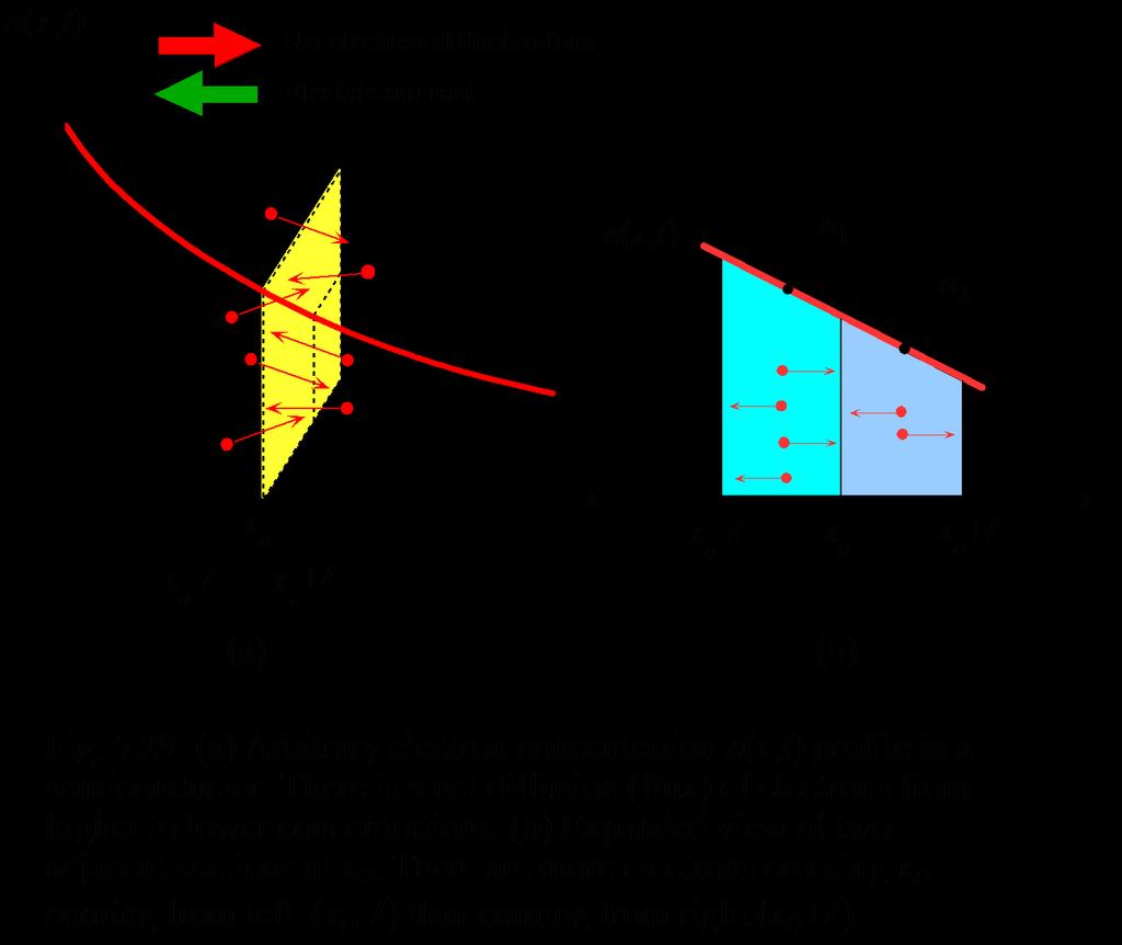
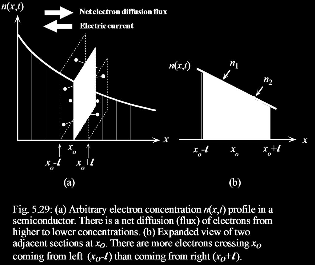
Motion and Recombination of Electrons and Holes
 Chater Motion and Recombination of Electrons and Holes OBJECTIVES. Understand how the electrons and holes resond to an electric field (drift).. Understand how the electrons and holes resond to a gradient
Electrical Transport. Ref. Ihn Ch. 10 YC, Ch 5; BW, Chs 4 & 8
 Electrical Transport Ref. Ihn Ch. 10 YC, Ch 5; BW, Chs 4 & 8 Electrical Transport The study of the transport of electrons & holes (in semiconductors) under various conditions. A broad & somewhat specialized
EE 346: Semiconductor Devices
 EE 346: Semiconductor Devices Lecture - 6 02/06/2017 Tewodros A. Zewde 1 DENSTY OF STATES FUNCTON Since current is due to the flow of charge, an important step in the process is to determine the number
Where µ n mobility of -e in C.B. µ p mobility of holes in V.B. And 2
 3.. Intrinsic semiconductors: Unbroken covalent bonds make a low conductivity crystal, and at 0 o k the crystal behaves as an insulator, since no free electrons and holes are available. At room temperature,
Semiconductor Physics Problems 2015
 Semiconductor Physics Problems 2015 Page and figure numbers refer to Semiconductor Devices Physics and Technology, 3rd edition, by SM Sze and M-K Lee 1. The purest semiconductor crystals it is possible
Solid State Physics SEMICONDUCTORS - IV. Lecture 25. A.H. Harker. Physics and Astronomy UCL
 Solid State Physics SEMICONDUCTORS - IV Lecture 25 A.H. Harker Physics and Astronomy UCL 9.9 Carrier diffusion and recombination Suppose we have a p-type semiconductor, i.e. n h >> n e. (1) Create a local
Semiconductors. SEM and EDAX images of an integrated circuit. SEM EDAX: Si EDAX: Al. Institut für Werkstoffe der ElektrotechnikIWE
 SEM and EDAX images of an integrated circuit SEM EDAX: Si EDAX: Al source: [Cal 99 / 605] M&D-.PPT, slide: 1, 12.02.02 Classification semiconductors electronic semiconductors mixed conductors ionic conductors
Unit IV Semiconductors Engineering Physics
 Introduction A semiconductor is a material that has a resistivity lies between that of a conductor and an insulator. The conductivity of a semiconductor material can be varied under an external electrical
EECS143 Microfabrication Technology
 EECS143 Microfabrication Technology Professor Ali Javey Introduction to Materials Lecture 1 Evolution of Devices Yesterday s Transistor (1947) Today s Transistor (2006) Why Semiconductors? Conductors e.g
V = IR or R = V I. R = ρ l A
 Metals and Semiconductors Ram Seshadri MRL 2031, x6129, seshadri@mrl.ucsb.edu Electrical resistance and Ohm s Law: If an electric current I (units of A, Ampère) flows through a conductor with resistance
ELECTRONIC I Lecture 1 Introduction to semiconductor. By Asst. Prof Dr. Jassim K. Hmood
 ELECTRONIC I Lecture 1 Introduction to semiconductor By Asst. Prof Dr. Jassim K. Hmood SOLID-STATE ELECTRONIC MATERIALS Electronic materials generally can be divided into three categories: insulators,
Electrical Properties
 Electrical Properties Electrical Conduction R Ohm s law V = IR I l Area, A V where I is current (Ampere), V is voltage (Volts) and R is the resistance (Ohms or ) of the conductor Resistivity Resistivity,
Junction Diodes. Tim Sumner, Imperial College, Rm: 1009, x /18/2006
 Junction Diodes Most elementary solid state junction electronic devices. They conduct in one direction (almost correct). Useful when one converts from AC to DC (rectifier). But today diodes have a wide
Chemistry Instrumental Analysis Lecture 8. Chem 4631
 Chemistry 4631 Instrumental Analysis Lecture 8 UV to IR Components of Optical Basic components of spectroscopic instruments: stable source of radiant energy transparent container to hold sample device
PHYS208 p-n junction. January 15, 2010
 1 PHYS208 p-n junction January 15, 2010 List of topics (1) Density of states Fermi-Dirac distribution Law of mass action Doped semiconductors Dopinglevel p-n-junctions 1 Intrinsic semiconductors List of
EE 446/646 Photovoltaic Devices I. Y. Baghzouz
 EE 446/646 Photovoltaic Devices I Y. Baghzouz What is Photovoltaics? First used in about 1890, the word has two parts: photo, derived from the Greek word for light, volt, relating to electricity pioneer
The Semiconductor in Equilibrium
 Lecture 6 Semiconductor physics IV The Semiconductor in Equilibrium Equilibrium, or thermal equilibrium No external forces such as voltages, electric fields. Magnetic fields, or temperature gradients are
ELECTRONIC DEVICES AND CIRCUITS SUMMARY
 ELECTRONIC DEVICES AND CIRCUITS SUMMARY Classification of Materials: Insulator: An insulator is a material that offers a very low level (or negligible) of conductivity when voltage is applied. Eg: Paper,
Basic Physics of Semiconductors
 Basic Physics of Semiconductors Semiconductor materials and their properties PN-junction diodes Reverse Breakdown EEM 205 Electronics I Dicle University, EEE Dr. Mehmet Siraç ÖZERDEM Semiconductor Physics
Mat E 272 Lecture 25: Electrical properties of materials
 Mat E 272 Lecture 25: Electrical properties of materials December 6, 2001 Introduction: Calcium and copper are both metals; Ca has a valence of +2 (2 electrons per atom) while Cu has a valence of +1 (1
MTLE-6120: Advanced Electronic Properties of Materials. Intrinsic and extrinsic semiconductors. Reading: Kasap:
 MTLE-6120: Advanced Electronic Properties of Materials 1 Intrinsic and extrinsic semiconductors Reading: Kasap: 5.1-5.6 Band structure and conduction 2 Metals: partially filled band(s) i.e. bands cross
Semiconductors. Semiconductors also can collect and generate photons, so they are important in optoelectronic or photonic applications.
 Semiconductors Semiconducting materials have electrical properties that fall between true conductors, (like metals) which are always highly conducting and insulators (like glass or plastic or common ceramics)
Lecture 7 - Carrier Drift and Diffusion (cont.) February 20, Non-uniformly doped semiconductor in thermal equilibrium
 February 20, Non-uniformly doped semiconductor in thermal equilibrium") 6.720J/3.43J - Integrated Microelectronic Devices - Spring 2007 Lecture 7-1 Lecture 7 - Carrier Drift and Diffusion (cont.) February 20, 2007 Contents: 1. Non-uniformly doped semiconductor in thermal equilibrium
6.720J/3.43J - Integrated Microelectronic Devices - Spring 2007 Lecture 7-1 Lecture 7 - Carrier Drift and Diffusion (cont.) February 20, 2007 Contents: 1. Non-uniformly doped semiconductor in thermal equilibrium
Classification of Solids
 Classification of Solids Classification by conductivity, which is related to the band structure: (Filled bands are shown dark; D(E) = Density of states) Class Electron Density Density of States D(E) Examples
Density of states for electrons and holes. Distribution function. Conduction and valence bands
 Intrinsic Semiconductors In the field of semiconductors electrons and holes are usually referred to as free carriers, or simply carriers, because it is these particles which are responsible for carrying
Semiconductor physics I. The Crystal Structure of Solids
 Lecture 3 Semiconductor physics I The Crystal Structure of Solids 1 Semiconductor materials Types of solids Space lattices Atomic Bonding Imperfection and doping in SOLIDS 2 Semiconductor Semiconductors
The Periodic Table III IV V
 The Periodic Table III IV V Slide 1 Electronic Bonds in Silicon 2-D picture of perfect crystal of pure silicon; double line is a Si-Si bond with each line representing an electron Si ion (charge +4 q)