ECE 340 Lecture 21 : P-N Junction II Class Outline:
|
|
|
- Evangeline Oliver
- 5 years ago
- Views:
Transcription
1 ECE 340 Lecture 21 : P-N Junction II Class Outline: Contact Potential Equilibrium Fermi Levels
2 Things you should know when you leave Key Questions What is the contact potential? Where does the transition region come from? How can I understand the contact potential quantitatively? What is the depletion approximation?
3 Contact Potential Now let s start analyzing the p-n junction We want to form a compromise between a very detailed description of the physics of the p-n junction and a solid qualitative understanding of its operation We have two different models: P-type N-type 1. Step junction (alloyed and epitaxial junctions) 2. Graded junctions (diffused junctions where N d N a varies over a significant distance across the junction) Our plan: Explore the step junction and extend the understanding to deal with the graded junction. Our starting point: We are starting in equilibrium with no external excitation and no external currents.
4 Contact Potential What do we expect to happen when we join them together? P-type N-type We expect to find the following when we connect the p-type semiconductor with the n-type semiconductor: The potential difference between the two regions resulting from the doping discrepancy will cause a potential difference between the two regions. There should be four components of current across the junction due to drift and diffusion. The four components must add to give zero net current at equilibrium.
5 Contact Potential But we already know what will happen when we join them together P-type N-type W Contact Potential φ p (diff) φ p (drift) φ n (diff) φ n (drift) J p (diff) J p (drift) J n (diff) J n (drift) Dashed Arrows = Particle Flow Solid Arrows = Resulting Currents
6 Contact Potential So what is the contact potential Contact Potential The contact potential is the voltage necessary to maintain equilibrium at the junction. The contact potential does not imply the presence of an external potential. The contact potential cannot be measured because when contact is made to the junction a potential forms at the contacts which works to cancel the contact potential. The contact potential also separates the bands with the conduction energy bands higher on the p-side. This is required to make the Fermi level constant.
7 Contact Potential Let s begin to develop a quantitative relationship for the contact potential Let s start by developing a relationship between the contact potential (V 0 ) and the doping concentrations on either side of the junction Begin with the current densities J J n p ( x) = qµ n( x) E( x) n ( x) = qµ p( x) E( x) p Drift + qd n qd p ( x) dn dx dp ( x) dx Diffusion Electrons Holes Focus for the moment on the hole current. In equilibrium, the different components should cancel. J ( x) = q p( x) E( x) p µ p qd dp dx ( x) p = 0
8 Contact Potential Now begin to simplify the equation Relate the electric field in the above equation to the gradient in the potential, and apply the Einstein relations. After we arrive at: Einstein Relations D µ N N DP µ P = = kbt q kbt q This is a simple differential equation we can solve by integration. But what are the limits? What we want: 1. Potential on either side of the junction (V N and V P ). 2. Hole concentration on either side of the junction.
9 Contact Potential Now we assume that we are dealing with a step-potential In doing so we can further assume that the electron and hole concentrations outside of the transition region are at their equilibrium values. So let s integrate Minority carriers Contact potential Majority carriers Finish representing the contact potential by relating it to the hole (or electron) concentrations on either side of the junction N-side donors But this may not be the most useful as we are often dealing with extrinsic semiconductors, so let s rewrite it P-side acceptors
10 Contact Potential By assuming the majority carrier concentration to be the doping, we can find another form of the equation Using the equilibrium carrier concentration equations, we can extend the above equation to include the electron concentrations on either side of the junction Will be useful later when we apply bias.
11 Equilibrium Fermi Levels We are in equilibrium, so is this consistent with the definitions for the contact potential that we have just derived? Let s redefine the contact potential in terms of what we know about the equilibrium carrier concentrations that we assume to prevail far from the transition region ( E E ) Non-degenerate Semiconductor kbt n = Nce ( Ev E f ) kbt p = N e v f c Energy bands are separated by the contact potential. Fermi levels on either side of the junction are equal in equilibrium. When we apply bias, the contact potential is lowered and the Fermi levels change.
12 Depletion Approximation To gain a qualitative understanding of the solution for the electrostatic variables we need Poisson s equation: Most times a simple closed form solution will not be possible, so we need an approximation from which we can derive other relations. Consider the following Doping profile is known To obtain the electric field and potential we need to integrate. However, we don t know the electron and hole concentrations as a function of x. Electron and hole concentrations are a function of the potential which we do not know until we solve Poisson s equation. Use the depletion approximation
13 Depletion Approximation We already have the foundation for this approximation A prominent feature in the qualitative solution was the appearance of a nonzero charge density straddling the junction. The charge arises because the carrier numbers are reduced by diffusion across the junction. The carrier depletion tends to be greatest in the immediate vicinity of the junction.

14 Depletion Approximation What does the depletion approximation tell us 1. The carrier concentrations are assumed to be negligible compared to the net doping concentrations in the junction region. 2. The charge density outside the depletion region is taken to be identically zero. Poisson equation becomes
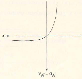
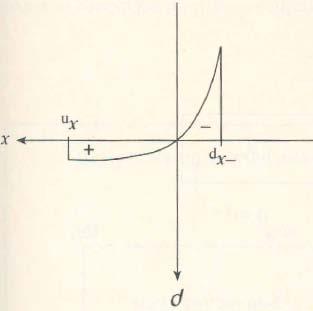

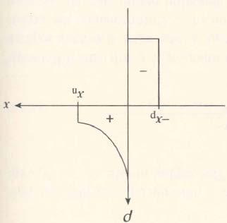
15 Depletion Approximation What does the depletion approximation look like
16 Problems Let s solve a few problems: A silicon step junction is maintained at room temperature with doping concentrations such that E F = E V 2kT on the p-side and E F = E C E G /4 on the n- side. (a) Draw the band diagram (b) Determine the contact potential N A (x) Consider the p1-p2 isotope junction shown here: (a) Draw the band diagram for the junction taking the doping to be non-degenerate and N A1 > N A2. (b) Derive an expression for the contact potential. (c) Make rough sketches of the electric field, potential and charge density. x
ECE 440 Lecture 28 : P-N Junction II Class Outline:
 ECE 440 Lecture 28 : P-N Junction II Class Outline: Contact Potential Equilibrium Fermi Levels Things you should know when you leave Key Questions What is the contact potential? Where does the transition
ECE 440 Lecture 20 : PN Junction Electrostatics II Class Outline:
 ECE 440 Lecture 20 : PN Junction Electrostatics II Class Outline: Depletion Approximation Step Junction Things you should know when you leave Key Questions What is the space charge region? What are the
ECE 440 Lecture 12 : Diffusion of Carriers Class Outline:
 ECE 440 Lecture 12 : Diffusion of Carriers Class Outline: Band Bending Diffusion Processes Diffusion and Drift of Carriers Things you should know when you leave Key Questions How do I calculate kinetic
Diodes. anode. cathode. cut-off. Can be approximated by a piecewise-linear-like characteristic. Lecture 9-1
 Diodes mplest nonlinear circuit element Basic operation sets the foundation for Bipolar Junction Transistors (BJTs) Also present in Field Effect Transistors (FETs) Ideal diode characteristic anode cathode
ECE-305: Spring Carrier Action: II. Pierret, Semiconductor Device Fundamentals (SDF) pp
 pp") ECE-305: Spring 015 Carrier Action: II Pierret, Semiconductor Device Fundamentals (SDF) pp. 89-104 Professor Mark Lundstrom Electrical and Computer Engineering Purdue University, West Lafayette, IN USA
ECE-305: Spring 015 Carrier Action: II Pierret, Semiconductor Device Fundamentals (SDF) pp. 89-104 Professor Mark Lundstrom Electrical and Computer Engineering Purdue University, West Lafayette, IN USA
Semiconductor Device Physics
 1 Semiconductor Device Physics Lecture 3 http://zitompul.wordpress.com 2 0 1 3 Semiconductor Device Physics 2 Three primary types of carrier action occur inside a semiconductor: Drift: charged particle
Charge Carriers in Semiconductor
 Charge Carriers in Semiconductor To understand PN junction s IV characteristics, it is important to understand charge carriers behavior in solids, how to modify carrier densities, and different mechanisms
PHYS208 P-N Junction. Olav Torheim. May 30, 2007
 1 PHYS208 P-N Junction Olav Torheim May 30, 2007 1 Intrinsic semiconductors The lower end of the conduction band is a parabola, just like in the quadratic free electron case (E = h2 k 2 2m ). The density
Semiconductor Physics and Devices
 The pn Junction 1) Charge carriers crossing the junction. 3) Barrier potential Semiconductor Physics and Devices Chapter 8. The pn Junction Diode 2) Formation of positive and negative ions. 4) Formation
Lecture 4 - PN Junction and MOS Electrostatics (I) Semiconductor Electrostatics in Thermal Equilibrium September 20, 2005
 Semiconductor Electrostatics in Thermal Equilibrium September 20, 2005") 6.012 - Microelectronic Devices and Circuits - Fall 2005 Lecture 4-1 Contents: Lecture 4 - PN Junction and MOS Electrostatics (I) Semiconductor Electrostatics in Thermal Equilibrium September 20, 2005
6.012 - Microelectronic Devices and Circuits - Fall 2005 Lecture 4-1 Contents: Lecture 4 - PN Junction and MOS Electrostatics (I) Semiconductor Electrostatics in Thermal Equilibrium September 20, 2005
Lecture 4 - PN Junction and MOS Electrostatics (I) Semiconductor Electrostatics in Thermal Equilibrium. February 13, 2003
 Semiconductor Electrostatics in Thermal Equilibrium. February 13, 2003") 6.012 - Microelectronic Devices and Circuits - Spring 2003 Lecture 4-1 Contents: Lecture 4 - PN Junction and MOS Electrostatics (I) Semiconductor Electrostatics in Thermal Equilibrium February 13, 2003
6.012 - Microelectronic Devices and Circuits - Spring 2003 Lecture 4-1 Contents: Lecture 4 - PN Junction and MOS Electrostatics (I) Semiconductor Electrostatics in Thermal Equilibrium February 13, 2003
EECS130 Integrated Circuit Devices
 EECS130 Integrated Circuit Devices Professor Ali Javey 9/18/2007 P Junctions Lecture 1 Reading: Chapter 5 Announcements For THIS WEEK OLY, Prof. Javey's office hours will be held on Tuesday, Sept 18 3:30-4:30
Semiconductor Physics fall 2012 problems
 Semiconductor Physics fall 2012 problems 1. An n-type sample of silicon has a uniform density N D = 10 16 atoms cm -3 of arsenic, and a p-type silicon sample has N A = 10 15 atoms cm -3 of boron. For each
Consider a uniformly doped PN junction, in which one region of the semiconductor is uniformly doped with acceptor atoms and the adjacent region is
 CHAPTER 7 The PN Junction Consider a uniformly doped PN junction, in which one region of the semiconductor is uniformly doped with acceptor atoms and the adjacent region is uniformly doped with donor atoms.
Chapter 7. The pn Junction
 Chapter 7 The pn Junction Chapter 7 PN Junction PN junction can be fabricated by implanting or diffusing donors into a P-type substrate such that a layer of semiconductor is converted into N type. Converting
Semiconductor Junctions
 8 Semiconductor Junctions Almost all solar cells contain junctions between different materials of different doping. Since these junctions are crucial to the operation of the solar cell, we will discuss
Midterm I - Solutions
 UNIVERSITY OF CALIFORNIA College of Engineering Department of Electrical Engineering and Computer Sciences EECS 130 Spring 2008 Professor Chenming Hu Midterm I - Solutions Name: SID: Grad/Undergrad: Closed
ECE 142: Electronic Circuits Lecture 3: Semiconductors
 Faculty of Engineering ECE 142: Electronic Circuits Lecture 3: Semiconductors Agenda Intrinsic Semiconductors Extrinsic Semiconductors N-type P-type Carrier Transport Drift Diffusion Semiconductors A semiconductor
Lecture 7 - Carrier Drift and Diffusion (cont.) February 20, Non-uniformly doped semiconductor in thermal equilibrium
 February 20, Non-uniformly doped semiconductor in thermal equilibrium") 6.720J/3.43J - Integrated Microelectronic Devices - Spring 2007 Lecture 7-1 Lecture 7 - Carrier Drift and Diffusion (cont.) February 20, 2007 Contents: 1. Non-uniformly doped semiconductor in thermal equilibrium
6.720J/3.43J - Integrated Microelectronic Devices - Spring 2007 Lecture 7-1 Lecture 7 - Carrier Drift and Diffusion (cont.) February 20, 2007 Contents: 1. Non-uniformly doped semiconductor in thermal equilibrium
Session 6: Solid State Physics. Diode
 Session 6: Solid State Physics Diode 1 Outline A B C D E F G H I J 2 Definitions / Assumptions Homojunction: the junction is between two regions of the same material Heterojunction: the junction is between
Fundamentals of Semiconductor Physics
 Fall 2007 Fundamentals of Semiconductor Physics 万 歆 Zhejiang Institute of Modern Physics xinwan@zimp.zju.edu.cn http://zimp.zju.edu.cn/~xinwan/ Transistor technology evokes new physics The objective of
Lecture 8 - Carrier Drift and Diffusion (cont.) September 21, 2001
 September 21, 2001") 6.720J/3.43J - Integrated Microelectronic Devices - Fall 2001 Lecture 8-1 Lecture 8 - Carrier Drift and Diffusion (cont.) September 21, 2001 Contents: 1. Non-uniformly doped semiconductor in thermal equilibrium
6.720J/3.43J - Integrated Microelectronic Devices - Fall 2001 Lecture 8-1 Lecture 8 - Carrier Drift and Diffusion (cont.) September 21, 2001 Contents: 1. Non-uniformly doped semiconductor in thermal equilibrium
UNIVERSITY OF CALIFORNIA College of Engineering Department of Electrical Engineering and Computer Sciences. EECS 130 Professor Ali Javey Fall 2006
 UNIVERSITY OF CALIFORNIA College of Engineering Department of Electrical Engineering and Computer Sciences EECS 130 Professor Ali Javey Fall 2006 Midterm I Name: Closed book. One sheet of notes is allowed.
Semiconductor Physics. Lecture 3
 Semiconductor Physics Lecture 3 Intrinsic carrier density Intrinsic carrier density Law of mass action Valid also if we add an impurity which either donates extra electrons or holes the number of carriers
Lecture 15 - The pn Junction Diode (I) I-V Characteristics. November 1, 2005
 I-V Characteristics. November 1, 2005") 6.012 - Microelectronic Devices and Circuits - Fall 2005 Lecture 15-1 Lecture 15 - The pn Junction Diode (I) I-V Characteristics November 1, 2005 Contents: 1. pn junction under bias 2. I-V characteristics
6.012 - Microelectronic Devices and Circuits - Fall 2005 Lecture 15-1 Lecture 15 - The pn Junction Diode (I) I-V Characteristics November 1, 2005 Contents: 1. pn junction under bias 2. I-V characteristics
Solid State Physics SEMICONDUCTORS - IV. Lecture 25. A.H. Harker. Physics and Astronomy UCL
 Solid State Physics SEMICONDUCTORS - IV Lecture 25 A.H. Harker Physics and Astronomy UCL 9.9 Carrier diffusion and recombination Suppose we have a p-type semiconductor, i.e. n h >> n e. (1) Create a local
PHYS208 p-n junction. January 15, 2010
 1 PHYS208 p-n junction January 15, 2010 List of topics (1) Density of states Fermi-Dirac distribution Law of mass action Doped semiconductors Dopinglevel p-n-junctions 1 Intrinsic semiconductors List of
UNIVERSITY OF CALIFORNIA College of Engineering Department of Electrical Engineering and Computer Sciences. EECS 130 Professor Ali Javey Fall 2006
 UNIVERSITY OF CALIFORNIA College of Engineering Department of Electrical Engineering and Computer Sciences EECS 130 Professor Ali Javey Fall 2006 Midterm 2 Name: SID: Closed book. Two sheets of notes are
CLASS 12th. Semiconductors
 CLASS 12th Semiconductors 01. Distinction Between Metals, Insulators and Semi-Conductors Metals are good conductors of electricity, insulators do not conduct electricity, while the semiconductors have
PN Junctions. Lecture 7
 Lecture 7 PN Junctions Kathy Aidala Applied Physics, G2 Harvard University 10 October, 2002 Wei 1 Active Circuit Elements Why are they desirable? Much greater flexibility in circuit applications. What
For the following statements, mark ( ) for true statement and (X) for wrong statement and correct it.
 for true statement and (X) for wrong statement and correct it.") Benha University Faculty of Engineering Shoubra Electrical Engineering Department First Year communications. Answer all the following questions Illustrate your answers with sketches when necessary. The
Benha University Faculty of Engineering Shoubra Electrical Engineering Department First Year communications. Answer all the following questions Illustrate your answers with sketches when necessary. The
Lecture 3 Semiconductor Physics (II) Carrier Transport
 Carrier Transport") Lecture 3 Semiconductor Physics (II) Carrier Transport Thermal Motion Carrier Drift Carrier Diffusion Outline Reading Assignment: Howe and Sodini; Chapter 2, Sect. 2.4-2.6 6.012 Spring 2009 Lecture 3 1
Lecture 3 Semiconductor Physics (II) Carrier Transport Thermal Motion Carrier Drift Carrier Diffusion Outline Reading Assignment: Howe and Sodini; Chapter 2, Sect. 2.4-2.6 6.012 Spring 2009 Lecture 3 1
Spring Semester 2012 Final Exam
 Spring Semester 2012 Final Exam Note: Show your work, underline results, and always show units. Official exam time: 2.0 hours; an extension of at least 1.0 hour will be granted to anyone. Materials parameters
ECE-305: Spring 2018 Exam 2 Review
 ECE-305: Spring 018 Exam Review Pierret, Semiconductor Device Fundamentals (SDF) Chapter 3 (pp. 75-138) Chapter 5 (pp. 195-6) Professor Peter Bermel Electrical and Computer Engineering Purdue University,
V BI. H. Föll: kiel.de/matwis/amat/semi_en/kap_2/backbone/r2_2_4.html. different electrochemical potentials (i.e.
 Consider the the band diagram for a homojunction, formed when two bits of the same type of semicondutor (e.g. Si) are doped p and ntype and then brought into contact. Electrons in the two bits have different
n N D n p = n i p N A
 Summary of electron and hole concentration in semiconductors Intrinsic semiconductor: E G n kt i = pi = N e 2 0 Donor-doped semiconductor: n N D where N D is the concentration of donor impurity Acceptor-doped
ESE 372 / Spring 2013 / Lecture 5 Metal Oxide Semiconductor Field Effect Transistor
 Metal Oxide Semiconductor Field Effect Transistor V G V G 1 Metal Oxide Semiconductor Field Effect Transistor We will need to understand how this current flows through Si What is electric current? 2 Back
Lecture 2. OUTLINE Basic Semiconductor Physics (cont d) PN Junction Diodes. Reading: Chapter Carrier drift and diffusion
 PN Junction Diodes. Reading: Chapter Carrier drift and diffusion") Lecture 2 OUTLIE Basic Semiconductor Physics (cont d) Carrier drift and diffusion P unction Diodes Electrostatics Caacitance Reading: Chater 2.1 2.2 EE105 Sring 2008 Lecture 1, 2, Slide 1 Prof. Wu, UC
Lecture 2 OUTLIE Basic Semiconductor Physics (cont d) Carrier drift and diffusion P unction Diodes Electrostatics Caacitance Reading: Chater 2.1 2.2 EE105 Sring 2008 Lecture 1, 2, Slide 1 Prof. Wu, UC
16EC401 BASIC ELECTRONIC DEVICES UNIT I PN JUNCTION DIODE. Energy Band Diagram of Conductor, Insulator and Semiconductor:
 16EC401 BASIC ELECTRONIC DEVICES UNIT I PN JUNCTION DIODE Energy bands in Intrinsic and Extrinsic silicon: Energy Band Diagram of Conductor, Insulator and Semiconductor: 1 2 Carrier transport: Any motion
ECE 340 Lecture 27 : Junction Capacitance Class Outline:
 ECE 340 Lecture 27 : Junction Capacitance Class Outline: Breakdown Review Junction Capacitance Things you should know when you leave M.J. Gilbert ECE 340 Lecture 27 10/24/11 Key Questions What types of
UNIVERSITY OF CALIFORNIA College of Engineering Department of Electrical Engineering and Computer Sciences. Professor Chenming Hu.
 UNIVERSITY OF CALIFORNIA College of Engineering Department of Electrical Engineering and Computer Sciences EECS 130 Spring 2009 Professor Chenming Hu Midterm I Name: Closed book. One sheet of notes is
Carriers Concentration and Current in Semiconductors
 Carriers Concentration and Current in Semiconductors Carrier Transport Two driving forces for carrier transport: electric field and spatial variation of the carrier concentration. Both driving forces lead
Introductory Nanotechnology ~ Basic Condensed Matter Physics ~
 Introductory Nanotechnology ~ Basic Condensed Matter Physics ~ Atsufumi Hirohata Department of Electronics Quick Review over the Last Lecture Classic model : Dulong-Petit empirical law c V, mol 3R 0 E
Review 5 unknowns: n(x,t), p(x,t), J e. Doping profile problems Electrostatic potential Poisson's equation. (x,t), J h
, p(x,t), J e. Doping profile problems Electrostatic potential Poisson's equation. (x,t), J h") 6.012 - Electronic Devices and Circuits Lecture 3 - Solving The Five Equations - Outline Announcements Handouts - 1. Lecture; 2. Photoconductivity; 3. Solving the 5 eqs. See website for Items 2 and 3.
6.012 - Electronic Devices and Circuits Lecture 3 - Solving The Five Equations - Outline Announcements Handouts - 1. Lecture; 2. Photoconductivity; 3. Solving the 5 eqs. See website for Items 2 and 3.
Quiz #1 Practice Problem Set
 Name: Student Number: ELEC 3908 Physical Electronics Quiz #1 Practice Problem Set? Minutes January 22, 2016 - No aids except a non-programmable calculator - All questions must be answered - All questions
Qualitative Picture of the Ideal Diode. G.R. Tynan UC San Diego MAE 119 Lecture Notes
 Qualitative Picture of the Ideal Diode G.R. Tynan UC San Diego MAE 119 Lecture Notes Band Theory of Solids: From Single Attoms to Solid Crystals Isolated Li atom (conducting metal) Has well-defined, isolated
Carrier transport: Drift and Diffusion
 . Carrier transport: Drift and INEL 5209 - Solid State Devices - Spring 2012 Manuel Toledo April 10, 2012 Manuel Toledo Transport 1/ 32 Outline...1 Drift Drift current Mobility Resistivity Resistance Hall
Electronic Devices and Circuits Lecture 5 - p-n Junction Injection and Flow - Outline
 6.012 - Electronic Devices and Circuits Lecture 5 - p-n Junction Injection and Flow - Outline Review Depletion approimation for an abrupt p-n junction Depletion charge storage and depletion capacitance
Electronic Circuits for Mechatronics ELCT 609 Lecture 2: PN Junctions (1)
") Electronic Circuits for Mechatronics ELCT 609 Lecture 2: PN Junctions (1) Assistant Professor Office: C3.315 E-mail: eman.azab@guc.edu.eg 1 Electronic (Semiconductor) Devices P-N Junctions (Diodes): Physical
Electronic Circuits for Mechatronics ELCT 609 Lecture 2: PN Junctions (1) Assistant Professor Office: C3.315 E-mail: eman.azab@guc.edu.eg 1 Electronic (Semiconductor) Devices P-N Junctions (Diodes): Physical
( )! N D ( x) ) and equilibrium
! N D ( x) ) and equilibrium") ECE 66: SOLUTIONS: ECE 66 Homework Week 8 Mark Lundstrom March 7, 13 1) The doping profile for an n- type silicon wafer ( N D = 1 15 cm - 3 ) with a heavily doped thin layer at the surface (surface concentration,
ECE 66: SOLUTIONS: ECE 66 Homework Week 8 Mark Lundstrom March 7, 13 1) The doping profile for an n- type silicon wafer ( N D = 1 15 cm - 3 ) with a heavily doped thin layer at the surface (surface concentration,
Isolated atoms Hydrogen Energy Levels. Neuromorphic Engineering I. Solids Energy bands. Metals, semiconductors and insulators Energy bands
 Isolated atoms Hydrogen Energy Levels Neuromorphic Engineering I INI-404 227-1033-00 Electron in atoms have quantized energy levels Material courtesy of Elisabetta Chicca Bielefeld University, Germany
Lecture 8 - Carrier Drift and Diffusion (cont.), Carrier Flow. February 21, 2007
, Carrier Flow. February 21, 2007") 6.720J/3.43J - Integrated Microelectronic Devices - Spring 2007 Lecture 8-1 Lecture 8 - Carrier Drift and Diffusion (cont.), Carrier Flow February 21, 2007 Contents: 1. Quasi-Fermi levels 2. Continuity
6.720J/3.43J - Integrated Microelectronic Devices - Spring 2007 Lecture 8-1 Lecture 8 - Carrier Drift and Diffusion (cont.), Carrier Flow February 21, 2007 Contents: 1. Quasi-Fermi levels 2. Continuity
FYS3410 Condensed matter physics
 FYS3410 Condensed matter physics Lecture 23 and 24: pn-junctions and electrooptics Randi Haakenaasen UniK/UiO Forsvarets forskningsinstitutt 11.05.2016 and 18.05.2016 Outline Why pn-junctions are important
1st Year-Computer Communication Engineering-RUC. 4- P-N Junction
 4- P-N Junction We begin our study of semiconductor devices with the junction for three reasons. (1) The device finds application in many electronic systems, e.g., in adapters that charge the batteries
Lecture 1. OUTLINE Basic Semiconductor Physics. Reading: Chapter 2.1. Semiconductors Intrinsic (undoped) silicon Doping Carrier concentrations
 silicon Doping Carrier concentrations") Lecture 1 OUTLINE Basic Semiconductor Physics Semiconductors Intrinsic (undoped) silicon Doping Carrier concentrations Reading: Chapter 2.1 EE105 Fall 2007 Lecture 1, Slide 1 What is a Semiconductor? Low
Lecture 1 OUTLINE Basic Semiconductor Physics Semiconductors Intrinsic (undoped) silicon Doping Carrier concentrations Reading: Chapter 2.1 EE105 Fall 2007 Lecture 1, Slide 1 What is a Semiconductor? Low
EE3901 A2001. Semiconductor Devices. Exam 1
 Name ECE Box # Problem Score Points 1 10 2 30 3 35 4 25 EE3901 A2001 Semiconductor Devices Exam 1 This is a closed book test! You are allowed one sheet (both sides) of notes. Note: Potentially useful reference
3. Consider a semiconductor. The concentration of electrons, n, in the conduction band is given by
 Colloqium problems to chapter 13 1. What is meant by an intrinsic semiconductor? n = p All the electrons are originating from thermal excitation from the valence band for an intrinsic semiconductor. Then
1 Name: Student number: DEPARTMENT OF PHYSICS AND PHYSICAL OCEANOGRAPHY MEMORIAL UNIVERSITY OF NEWFOUNDLAND. Fall :00-11:00
 1 Name: DEPARTMENT OF PHYSICS AND PHYSICAL OCEANOGRAPHY MEMORIAL UNIVERSITY OF NEWFOUNDLAND Final Exam Physics 3000 December 11, 2012 Fall 2012 9:00-11:00 INSTRUCTIONS: 1. Answer all seven (7) questions.
Engineering 2000 Chapter 8 Semiconductors. ENG2000: R.I. Hornsey Semi: 1
 Engineering 2000 Chapter 8 Semiconductors ENG2000: R.I. Hornsey Semi: 1 Overview We need to know the electrical properties of Si To do this, we must also draw on some of the physical properties and we
The 5 basic equations of semiconductor device physics: We will in general be faced with finding 5 quantities:
 6.012 - Electronic Devices and Circuits Solving the 5 basic equations - 2/12/08 Version The 5 basic equations of semiconductor device physics: We will in general be faced with finding 5 quantities: n(x,t),
Semiconductor Physics Problems 2015
 Semiconductor Physics Problems 2015 Page and figure numbers refer to Semiconductor Devices Physics and Technology, 3rd edition, by SM Sze and M-K Lee 1. The purest semiconductor crystals it is possible
6.012 Electronic Devices and Circuits
 Page 1 of 1 YOUR NAME Department of Electrical Engineering and Computer Science Massachusetts Institute of Technology 6.12 Electronic Devices and Circuits Exam No. 1 Wednesday, October 7, 29 7:3 to 9:3
Lecture 9 - Carrier Drift and Diffusion (cont.), Carrier Flow. September 24, 2001
, Carrier Flow. September 24, 2001") 6.720J/3.43J - Integrated Microelectronic Devices - Fall 2001 Lecture 9-1 Lecture 9 - Carrier Drift and Diffusion (cont.), Carrier Flow September 24, 2001 Contents: 1. Quasi-Fermi levels 2. Continuity
6.720J/3.43J - Integrated Microelectronic Devices - Fall 2001 Lecture 9-1 Lecture 9 - Carrier Drift and Diffusion (cont.), Carrier Flow September 24, 2001 Contents: 1. Quasi-Fermi levels 2. Continuity
Getting J e (x), J h (x), E(x), and p'(x), knowing n'(x) Solving the diffusion equation for n'(x) (using p-type example)
, J h (x), E(x), and p'(x), knowing n'(x) Solving the diffusion equation for n'(x) (using p-type example)") 6.012 - Electronic Devices and Circuits Lecture 4 - Non-uniform Injection (Flow) Problems - Outline Announcements Handouts - 1. Lecture Outline and Summary; 2. Thermoelectrics Review Thermoelectricity:
6.012 - Electronic Devices and Circuits Lecture 4 - Non-uniform Injection (Flow) Problems - Outline Announcements Handouts - 1. Lecture Outline and Summary; 2. Thermoelectrics Review Thermoelectricity:
Uniform excitation: applied field and optical generation. Non-uniform doping/excitation: diffusion, continuity
 6.012 - Electronic Devices and Circuits Lecture 2 - Uniform Excitation; Non-uniform conditions Announcements Review Carrier concentrations in TE given the doping level What happens above and below room
Final Examination EE 130 December 16, 1997 Time allotted: 180 minutes
 Final Examination EE 130 December 16, 1997 Time allotted: 180 minutes Problem 1: Semiconductor Fundamentals [30 points] A uniformly doped silicon sample of length 100µm and cross-sectional area 100µm 2
Semiconductor Physics
 Semiconductor Physics Motivation Is it possible that there might be current flowing in a conductor (or a semiconductor) even when there is no potential difference supplied across its ends? Look at the
Chapter 2. Electronics I - Semiconductors
 Chapter 2 Electronics I - Semiconductors Fall 2017 talarico@gonzaga.edu 1 Charged Particles The operation of all electronic devices is based on controlling the flow of charged particles There are two type
ECE-305: Fall 2016 Minority Carrier Diffusion Equation (MCDE)
") ECE-305: Fall 2016 Minority Carrier Diffusion Equation (MCDE) Professor Peter Bermel Electrical and Computer Engineering Purdue University, West Lafayette, IN USA pbermel@purdue.edu Pierret, Semiconductor
ECE-305: Fall 2016 Minority Carrier Diffusion Equation (MCDE) Professor Peter Bermel Electrical and Computer Engineering Purdue University, West Lafayette, IN USA pbermel@purdue.edu Pierret, Semiconductor
ECE 305 Exam 2: Spring 2017 March 10, 2017 Muhammad Alam Purdue University
 NAME: PUID: : ECE 305 Exam 2: Spring 2017 March 10, 2017 Muhammad Alam Purdue University This is a closed book exam You may use a calculator and the formula sheet Following the ECE policy, the calculator
Review Energy Bands Carrier Density & Mobility Carrier Transport Generation and Recombination
 Review Energy Bands Carrier Density & Mobility Carrier Transport Generation and Recombination The Metal-Semiconductor Junction: Review Energy band diagram of the metal and the semiconductor before (a)
Lecture-4 Junction Diode Characteristics
 1 Lecture-4 Junction Diode Characteristics Part-II Q: Aluminum is alloyed into n-type Si sample (N D = 10 16 cm 3 ) forming an abrupt junction of circular cross-section, with an diameter of 0.02 in. Assume
Holes (10x larger). Diode currents proportional to minority carrier densities on each side of the depletion region: J n n p0 = n i 2
. Diode currents proportional to minority carrier densities on each side of the depletion region: J n n p0 = n i 2") Part V. (40 pts.) A diode is composed of an abrupt PN junction with N D = 10 16 /cm 3 and N A =10 17 /cm 3. The diode is very long so you can assume the ends are at x =positive and negative infinity. 1.
Part V. (40 pts.) A diode is composed of an abrupt PN junction with N D = 10 16 /cm 3 and N A =10 17 /cm 3. The diode is very long so you can assume the ends are at x =positive and negative infinity. 1.
Section 12: Intro to Devices
 Section 12: Intro to Devices Extensive reading materials on reserve, including Robert F. Pierret, Semiconductor Device Fundamentals Bond Model of Electrons and Holes Si Si Si Si Si Si Si Si Si Silicon
PN Junction
 P Junction 2017-05-04 Definition Power Electronics = semiconductor switches are used Analogue amplifier = high power loss 250 200 u x 150 100 u Udc i 50 0 0 50 100 150 200 250 300 350 400 i,u dc i,u u
Electro - Principles I
 Electro - Principles I Page 10-1 Atomic Theory It is necessary to know what goes on at the atomic level of a semiconductor so the characteristics of the semiconductor can be understood. In many cases a
KATIHAL FİZİĞİ MNT-510
 KATIHAL FİZİĞİ MNT-510 YARIİLETKENLER Kaynaklar: Katıhal Fiziği, Prof. Dr. Mustafa Dikici, Seçkin Yayıncılık Katıhal Fiziği, Şakir Aydoğan, Nobel Yayıncılık, Physics for Computer Science Students: With
Fundamentals of the Metal Oxide Semiconductor Field-Effect Transistor
 Triode Working FET Fundamentals of the Metal Oxide Semiconductor Field-Effect Transistor The characteristics of energy bands as a function of applied voltage. Surface inversion. The expression for the
SEMICONDUCTOR DIODE. Unbiased (non-polarized) PN junction
 PN junction") SEMICONDUCTOR DIODE Semiconductor diode is an electronic element made of different types of extrinsic semiconductor: N-type semiconductor doped by donor impurities and P-type semiconductor doped by acceptor
SEMICONDUCTOR DIODE Semiconductor diode is an electronic element made of different types of extrinsic semiconductor: N-type semiconductor doped by donor impurities and P-type semiconductor doped by acceptor
ECE 442. Spring, Lecture -2
 ECE 442 Power Semiconductor Devices and Integrated circuits Spring, 2006 University of Illinois at Chicago Lecture -2 Semiconductor physics band structures and charge carriers 1. What are the types of
Semiconductor Physics fall 2012 problems
 Semiconductor Physics fall 2012 problems 1. An n-type sample of silicon has a uniform density N D = 10 16 atoms cm -3 of arsenic, and a p-type silicon sample has N A = 10 15 atoms cm -3 of boron. For each
Lecture 6 PN Junction and MOS Electrostatics(III) Metal-Oxide-Semiconductor Structure
 Metal-Oxide-Semiconductor Structure") Lecture 6 PN Junction and MOS Electrostatics(III) Metal-Oxide-Semiconductor Structure Outline 1. Introduction to MOS structure 2. Electrostatics of MOS in thermal equilibrium 3. Electrostatics of MOS with
Lecture 6 PN Junction and MOS Electrostatics(III) Metal-Oxide-Semiconductor Structure Outline 1. Introduction to MOS structure 2. Electrostatics of MOS in thermal equilibrium 3. Electrostatics of MOS with
Carrier Mobility and Hall Effect. Prof.P. Ravindran, Department of Physics, Central University of Tamil Nadu, India
 Carrier Mobility and Hall Effect 1 Prof.P. Ravindran, Department of Physics, Central University of Tamil Nadu, India http://folk.uio.no/ravi/semi2013 calculation Calculate the hole and electron densities
Band Alignment and Graded Heterostructures. Guofu Niu Auburn University
 Band Alignment and Graded Heterostructures Guofu Niu Auburn University Outline Concept of electron affinity Types of heterojunction band alignment Band alignment in strained SiGe/Si Cusps and Notches at
PN Junction and MOS structure
 PN Junction and MOS structure Basic electrostatic equations We will use simple one-dimensional electrostatic equations to develop insight and basic understanding of how semiconductor devices operate Gauss's
The German University in Cairo. Faculty of Information Engineering & Technology Semiconductors (Elct 503) Electronics Department Fall 2014
 Electronics Department Fall 2014") The German University in Cairo th Electronics 5 Semester Faculty of Information Engineering & Technology Semiconductors (Elct 503) Electronics Department Fall 2014 Problem Set 3 1- a) Find the resistivity
The German University in Cairo th Electronics 5 Semester Faculty of Information Engineering & Technology Semiconductors (Elct 503) Electronics Department Fall 2014 Problem Set 3 1- a) Find the resistivity
Numerical Example: Carrier Concentrations
 2 Numerical ample: Carrier Concentrations Donor concentration: N d = 10 15 cm -3 Thermal equilibrium electron concentration: n o N d = 10 15 cm 3 Thermal equilibrium hole concentration: 2 2 p o = n i no
ECE 335: Electronic Engineering Lecture 2: Semiconductors
 Faculty of Engineering ECE 335: Electronic Engineering Lecture 2: Semiconductors Agenda Intrinsic Semiconductors Extrinsic Semiconductors N-type P-type Carrier Transport Drift Diffusion Semiconductors
Peak Electric Field. Junction breakdown occurs when the peak electric field in the PN junction reaches a critical value. For the N + P junction,
 Peak Electric Field Junction breakdown occurs when the peak electric field in the P junction reaches a critical value. For the + P junction, qa E ( x) ( xp x), s W dep 2 s ( bi Vr ) 2 s potential barrier
Department of Electrical and Computer Engineering, Cornell University. ECE 3150: Microelectronics. Spring Exam 1 ` March 22, 2018
 Department of Electrical and Computer Engineering, Cornell University ECE 3150: Microelectronics Spring 2018 Exam 1 ` March 22, 2018 INSTRUCTIONS: Every problem must be done in the separate booklet Only
This is the 15th lecture of this course in which we begin a new topic, Excess Carriers. This topic will be covered in two lectures.
 Solid State Devices Dr. S. Karmalkar Department of Electronics and Communication Engineering Indian Institute of Technology, Madras Lecture - 15 Excess Carriers This is the 15th lecture of this course
EE105 Fall 2015 Microelectronic Devices and Circuits: Semiconductor Fabrication and PN Junctions
 EE105 Fall 2015 Microelectronic Devices and Circuits: Semiconductor Fabrication and PN Junctions Prof. Ming C. Wu wu@eecs.berkeley.edu 511 Sutardja Dai Hall (SDH) 1 pn Junction p-type semiconductor in
ECE 606 Homework Week 7 Mark Lundstrom Purdue University (revised 2/25/13) e E i! E T
 e E i! E T") ECE 606 Homework Week 7 Mark Lundstrom Purdue University (revised 2/25/13) 1) Consider an n- type semiconductor for which the only states in the bandgap are donor levels (i.e. ( E T = E D ). Begin with
ECE 606 Homework Week 7 Mark Lundstrom Purdue University (revised 2/25/13) 1) Consider an n- type semiconductor for which the only states in the bandgap are donor levels (i.e. ( E T = E D ). Begin with
collisions of electrons. In semiconductor, in certain temperature ranges the conductivity increases rapidly by increasing temperature
 1.9. Temperature Dependence of Semiconductor Conductivity Such dependence is one most important in semiconductor. In metals, Conductivity decreases by increasing temperature due to greater frequency of
L03: pn Junctions, Diodes
 8/30/2012 Page 1 of 5 Reference:C:\Users\Bernhard Boser\Documents\Files\Lib\MathCAD\Default\defaults.mcd L03: pn Junctions, Diodes Intrinsic Si Q: What are n, p? Q: Is the Si charged? Q: How could we make
Lecture 2. Introduction to semiconductors Structures and characteristics in semiconductors
 Lecture 2 Introduction to semiconductors Structures and characteristics in semiconductors Semiconductor p-n junction Metal Oxide Silicon structure Semiconductor contact Literature Glen F. Knoll, Radiation
Lecture (02) Introduction to Electronics II, PN Junction and Diodes I
 Introduction to Electronics II, PN Junction and Diodes I") Lecture (02) Introduction to Electronics II, PN Junction and Diodes I By: Dr. Ahmed ElShafee ١ Agenda Current in semiconductors/conductors N type, P type semiconductors N Type Semiconductor P Type Semiconductor
Lecture (02) Introduction to Electronics II, PN Junction and Diodes I By: Dr. Ahmed ElShafee ١ Agenda Current in semiconductors/conductors N type, P type semiconductors N Type Semiconductor P Type Semiconductor
Lecture 2. Introduction to semiconductors Structures and characteristics in semiconductors
 Lecture 2 Introduction to semiconductors Structures and characteristics in semiconductors Semiconductor p-n junction Metal Oxide Silicon structure Semiconductor contact Literature Glen F. Knoll, Radiation
Carriers Concentration, Current & Hall Effect in Semiconductors. Prof.P. Ravindran, Department of Physics, Central University of Tamil Nadu, India
 Carriers Concentration, Current & Hall Effect in Semiconductors 1 Prof.P. Ravindran, Department of Physics, Central University of Tamil Nadu, India http://folk.uio.no/ravi/semi2013 Conductivity Charge
ECE 340 Lecture 39 : MOS Capacitor II
 ECE 340 Lecture 39 : MOS Capacitor II Class Outline: Effects of Real Surfaces Threshold Voltage MOS Capacitance-Voltage Analysis Things you should know when you leave Key Questions What are the effects