CHAP.4 Circuit Characteristics and Performance Estimation
|
|
|
- Mark Sanders
- 5 years ago
- Views:
Transcription
 where ρ Resisiviy")
 in 0.5µm o 1.")
1 HAP.4 ircui haracerisics and Performance Esimaion 4. Resisance esimaion R ρ l w (ohms) where ρ Resisiviy Thickness l onducor lengh w onducor widh l R Rs w where Rs Shee resisance (Ω/square) in 0.5µm o 1.0µm MOS processes 00/4/18 1
2 * hannel resisance R c k W 1 gs 1 ( ) W µ ox gs 1 k, k 1,000~30,000Ω/square µ ( ) ox 1 gs Typical shee resisance for conducors (Table 4.1) hannel resisance + 0.5% per Meal and poly % per Well diffusion % per Resisance for nonrecangular regions (Fig 4.) 4.3 apaciance esimaion Running/Swiching speed of MOS Parasiic MOS capaciance + Runners (wired poly, meal, diffusion) x (device and conducor resisance) Toal loading capaciance 1. Gae capaciance (of oher inpu). Diffusion capaciance (of he drain regions) 3. Rouing capaciance (of connecions beween O/P & I/P) To esimae he speed of he device ( R and informaion) MOS-apacior haracerisics (**wihou Source and Drain) Accumulaion g < 0 Gae volage Depleion g 0 Inversion g > 0 00/4/18
3 (a) Accumulaion layer is direcly conneced o subsrae. Gae capaciance can be approximaed by o ε ε SiO 0 ox A (4.4) where A Area of gae Relaive permiiviy Of SiO 3.9 ЄSiO Dielecric consan Є0 Permiiviy of free space (b) Depleion mode : Funcion of : (1) Doping concenraion (N) () Elecronic charge (q) (3) Depleion deph (d) (c) Inversion 00/4/18 gb o in series wih dep, where gb(gae-o-bulk(subs)) 0 dep gb + (varied as a funcion of gs) dep ε 0 ( 1) dep 0 + εsi d dep dep A min ε Si, low frequency, high frequency ( < 100 Hz ) 3
 gb Gae-o-bulk capaciance (Inpu) Toal gae capaciance g of an MOS device (or so-called inpu capaciance) g gb + gs + gd")
 hannel is heavily invered pinch off gd 0 gs ε 0 ε SiO 3 ox A Approximaion of MOS gae capaciance")
4 MOS Device capaciance ircui symbol gs, gd Gae-o-channel capaciance (Inpu par) sb, db Source/drain diff-o-bulk (subs) capaciance (Oupu par) gb Gae-o-bulk capaciance (Inpu) Toal gae capaciance g of an MOS device (or so-called inpu capaciance) g gb + gs + gd (a) Off-region : ( gs < ) No channel gs gd 0 g gb o + dep (b) Non-sauraion region : ( gs - > ds ) gd gs ε0ε ox 0 gb 1 SiO A (c) Sauraed region : ( gs - < ds ) hannel is heavily invered pinch off gd 0 gs ε 0 ε SiO 3 ox A Approximaion of MOS gae capaciance 00/4/18 4
 g 0. 005pF ( λ 0.5µm ) Uni ransisor: A ransisor ha can be convenienly conneced o meal a boh source and drain. 4.3.")
 + ( a + b ) ja jp \" sidewall \" periphery where 1. ja: Juncion capaciance 4 4 pf / µ m (3 10 NMOS,5 10 PMOS).")
5 onservaive approximaion: g o ox A where ox : hin-oxide capaciance per uni area. ε0ε SiO 35 µ m ox ο ο 4 ( 17) 10 pf 100Α ~ 00Α ox () (W) (ox) 4 ( 1µ m) ( µ m) ( pf µ m ) g pF ( λ 0.5µm ) Uni ransisor: A ransisor ha can be convenienly conneced o meal a boh source and drain Diffusion (source and drain) capaciance d : Proporional o oal diffusion-o-subsrae juncion area 1. Base area +. he area of he ( ab ) + ( a + b ) ja jp " sidewall " periphery where 1. ja: Juncion capaciance 4 4 pf / µ m (3 10 NMOS,5 10 PMOS). jp: 4 4 Periphery capaciance pf / µ m (4 10 NMOS,4 10 PMOS) 3. a : Widh of diffusion area (µm) 4. b : engh of diffusion area (µm) 00/4/18 5
 b j Juncion volage (negaive for reverse bias) jo(a,p) Zero-bias capaciance (j 0) b Build-in juncion poenial ~0.6 Diffusion capaciance form sb and db in Fig.4.5 4.3.")

6 Thickness of depleion layer depends on he volage across he juncion, boh ja and jp are funcions of juncion volage (j) j ( a p) ( a, p) m j, jo 1 (m0.3~0.5) b j Juncion volage (negaive for reverse bias) jo(a,p) Zero-bias capaciance (j 0) b Build-in juncion poenial ~0.6 Diffusion capaciance form sb and db in Fig Rouing capaciance Rouing capaciance beween meal and poly layers and he subsrae can be modeled as a parallel-plae capaciance. ε A plus fringing field ha occurs a he edges of he conducor due o is finie hickness. Toal capaciance (a) Parallel-plae capaciance of widh (w-/) + (b) A cylindrical capaciance of radiaes (/) w π ε + h h h h ln Empirical formula w w ε h h h 00/4/18 6
7 In general, meal and poly lines have higher capaciance value han he prediced values (due o he fringing facor) Muliple conducor capaciance (Fig.4.11 and 4.1) Disribued R effecs ong wires arge R Transmission line effecs R-secion model dj d ( I I ) j 1 j ( j 1 j ) ( j j + 1) n( n + 1) R R n R (n: secion number) As number of secions increase Differenial equaions x disance from inpu d d rc r resisance per uni lengh d dx c capaciance per uni lengh x ( propagaion ime) kx ( wire of lengh x) rc 1 ( l lengh of he wire ) l Example : r 0 Ω µm, 4 c 4 10 pf µ m (a) Poly bus of -mm, 15 p 4 10 l 16ns (b) Poly bus (-mm) poly bus (1-mm) + buffer p ns + τ buf 15 ( 1000 ) + τ ( 1000 ) + 4 ns buf 8ns + τ buf 00/4/18 7
 As speed increases, meal layer will also have R effec Add buffer Widen he line ( R, increases a lile ) Shoren lengh ( l ) R delay model (imporan in calculaing clock disribuion in highspeed,")
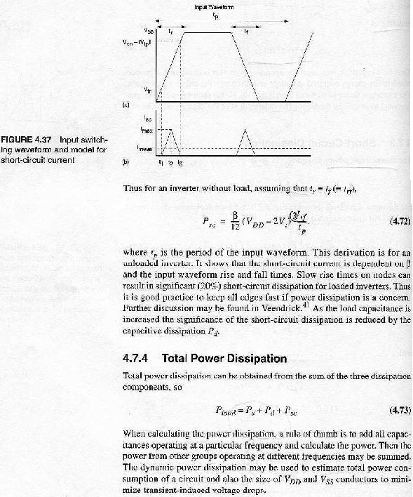
8 onusions: (a) Use poly for only local inerconnecion or very slow global inerconnecion in wo-meal process. (b) As speed increases, meal layer will also have R effec Add buffer Widen he line ( R, increases a lile ) Shoren lengh ( l ) R delay model (imporan in calculaing clock disribuion in highspeed, high-densiy chips), R : oal lumped R, of he line. τ rcl apaciance design guide (Sec.4.3.7) Wire-lengh design guide (Table 4.7) Inducance (Sec.4.4) 4.5 Swiching haracerisics Swiching speed : 1. Time o charge he load capacior oward. Time o discharge oward SS (a) Rise ime (r): Time for a waveform o rise from 10%~90% of is seady-sae value. (b) Fall ime (f): fall from 90%~10% (c) Delay ime(d): ime difference beween inpu ransiion (50%) and he 50% oupu level. 00/4/18 8
 (X dsgs-) (sauraion) (b) f ou drops from (-n) o 0.1 (dsgs- X3) (nonsauraion, linear mode) f1 (NMOS is in sauraion mode) d d ou ( ) 0 n + n (discharge curren is consan) f 1 f 1 0.")
9 Fall ime ( f ) : X1: NMOS u-off X: NMOS sauraed region X3: NMOS nonsauraion (inear mode) Analysis of f IN, (gs ), (iniial value) (a) f1 ou drops from 0.9 o (-n) (X dsgs-) (sauraion) (b) f ou drops from (-n) o 0.1 (dsgs- X3) (nonsauraion, linear mode) f1 (NMOS is in sauraion mode) d d ou ( ) 0 n + n (discharge curren is consan) f 1 f n ( ) n ( n 0.1 ) ( ) n n n d ou 00/4/18 9
10 f (NMOS is in linear mode) IN DS ou I DS n ( ) ou n ou d d ou n ( ) ou n ou ln 19 0 [ n] f n ( 1 n), n n/ f f f 1 + f k ( Eq.4.37 ) n ( k 3 ~ 4) Increases speed (How o opimize MOS circui speed?) - Reduce load capaciance - Increase n - ow supply volage low speed Rise ime ( p 0.1) ( 1 p) ( 19 p) r + ln 0 p p 1 p f k p ( k 3 ~ 4) Equal size n,p devices, np f r!! f r n p W p ( ~ 3) Wn 00/4/18 10
 Average gae delay for rising and falling ransiion av dr + df SPIE simulaion (Figure 4.0) Empirical delay model: Back subsiue ino Eqs. (4.46) & (4.47) o obain AN and AP for Wp Wn, AN AP 0.")
11 Delay ime * Approximaion: r f dr df An alernaive formula (a) 1 n ( 1 n) + ln ( ) df AN, AN n 1 n 1 n 0 (AN 0.83) wih nn/, 0ou/ 0 (b) dr A p A p p 0.83 (c) Average gae delay for rising and falling ransiion av dr + df SPIE simulaion (Figure 4.0) Empirical delay model: Back subsiue ino Eqs. (4.46) & (4.47) o obain AN and AP for Wp Wn, AN AP 0.36 dr 0.36 /n Gae delays For pull-down case W n W p, µ n1 n n3 ox W 1 n neff n1 n ( ) n3 00/4/18 11
 Mobiliy difference Graphical undersanding n, f k n 3 串聯 f r 1 Graphical Rule n series 3 W µ ox τ series k n 3 Fall ime: m n-devices in series f`m f Rise ime: m p-devices in series r`m r Fall ime:")
12 For pull-up case: p,eff p (only one urns on), p,eff 3p (hree urn on) For p 0.3 n r k ( 0.3 ) Mobiliy difference Graphical undersanding n, f k n 3 串聯 f r 1 Graphical Rule n series 3 W µ ox τ series k n 3 Fall ime: m n-devices in series f`m f Rise ime: m p-devices in series r`m r Fall ime: m n-devices in parallel (all urn on) f`f/m Rise ime: m p-devices in parallel (all urn on) r`r/m Swich-level R models 00/4/18 1
 Ri Summed Resisance from d Σ Ri i poin i o power or ground i apaciance a poin i df (RN1 cd)+[(rn1+rn) bc]+[(rn1+rn+rn3) ab]+[(rn1+rn+rn3+rn4)")
13 (A) Simple R model : (R, are lumped ogeher) df Σ Rpulldown Σ pulldown-pah dr (RN1+RN+ RN3+RN4) (ou+ab+ bc+cd) Rp ou Effecive Resisance R Reff (/W) (B) Penfield-Rubensein model : calculae delays in generalized R ree (ladder) Ri Summed Resisance from d Σ Ri i poin i o power or ground i apaciance a poin i df (RN1 cd)+[(rn1+rn) bc]+[(rn1+rn+rn3) ab]+[(rn1+rn+rn3+rn4) ou] Macro modeling (Daa book) Tswin: Inpu waveform in: Inpu capaciance Tbeou: Delay hrough he gae Tswou: Oupu waveform : Oupu capaciance In ASI designs, logic gaes are reaed as simple delay elemens. d inernal + k oupu Oupu delay, which is proporional o oupu loading capaciance. Fixed inernal delay. 00/4/18 13

14 SPIE Simulaion Experimens: * Parameer Example: r k.1ns f k 3.8ns ( k is in pf ) 00/4/18 14
 (3) Nodes cd, bc, and ab are a an n-hreshold below (~3.1vols). When N1B urns on.")
15 Body effec (1) Body Effec: γ sb (hange in hreshold volage is a funcion of Source-o-subsrae bias volage). Beer Bad () Poin D rises o abou 1.7vols before being discharged o ground ( 上圖所示 ) (3) Nodes cd, bc, and ab are a an n-hreshold below (~3.1vols). When N1B urns on. Nodes ab,bc,and cd are pulled o ground in ha order ( 下圖所示 ) (4) When >> inernal cap, his effec can be minimized. Sraegy o handle Body effec (1) Place ransisors wih laes arriving signals neares he oupu of he gae. The early signals discharge inernal nodes, and he body effec is minimized. () Minimize inernal capaciances: If diffusion wire is used o minimize he gae geomery, ry o use i a he oupu raher han on some inernal nodes. (3) Body effec is essenially a dynamic problem involving he charging of parasiic capaciances. * onclusion of Secion 4.5: Model of ransisors and parasiic capaciances mus be accurae so ha AD ools can work well. 00/4/18 15
16 4.6 MOS-Gae Transisor Sizing * For rf, Wp(-3)Wn Increase layou area and dynamic power consumpion. *Approximaed delay for an inverer pair (a) inv-pair f + r (WpWn) R(3eq) + ( R )(3eq) 3Req +3 Req 6Req R ON Res of a uni-size ransisor eqg+d (gae and diffusion cap.) (b) inv-pair (WpWn) R(eq)+()(R)(eq) fall rise 6Req * n/p raio rise / fall inv (Inverer hreshold volage) inv dd+p+n 1+ n p n p, (Eg.4) whennp, n p invdd/ In self-loaded circuis minimum-sized devices may be used o reduce power dissipaion and increase circui packaging densiy. When he circuis have o drive any significan rouing load, his opimizaion does no apply and he n- and p- devices should be sized o yield equal rise and fall ime. 00/4/18 16
17 4.6. Sage raio (Transisor Sizing skills) * Used in applicaions of (1) ong bus () I/O Buffers (3) Pads (4) Off-chip capaciive load To minimize he delay beween inpu and oupu while minimizing he area and power dissipaion. d: he average delay of a minimum-sized inverer driving anoher minimum-sized inverer. Delay of each sage (d ): R R/a, a d a d n-sage n(a d ) Toal delay /gra n ( produc of n sages) n lnr lna Toal delay lnr lna a d (Noe ha lnr, d are consans) Minimum delay ae (.714) 00/4/18 17
18 4.7 Power dissipaion MOS power sources: (1) Ps: Saic dissipaions (leakage curren) () Pd: Dynamic dissipaions - Swiching ransien curren from dd o GND. - The Energy/power o charge and discharge Saic Power Dissipaion >No curren > Ps0, Reverse-biased parasiic diodes (leakage curren) eakage curren : i o is (e qv /KT -1) 0.1nA~0.5nA per device a room emperaure. where is: Reverse sauraion curren v: Diode volage Ps n leakage curren x supply volage, 1 where n oal device number 00/4/18 18
19 4.7. Dynamic Power Dissipaion 0 1,1 0 n,p devices are boh on Shor circui curren pulse from dd o ss As he increases, he discharge or charge currens sar o dominae he curren drawn from he power suppliers. 00/4/18 19
20 ** Dynamic Power Dissipaion: harge/discharge *Pd 1 p/ p in() ou d + 1 p 0 p ip() (dd-ou) d p/ in() n-device ransien curren dou d ip() p-device ransien curren d(dd-ou) d Pd Average dynamic power o charge/discharge Pd dd p ou dou + 0 p (dd-ou) d(dd-ou) 0 dd dd / p dd fp 00/4/18 0
21 00/4/18 1
22 4.7.3 Shor-circui dissipaion PscImean * dd I mean [ 1 T 1 3 I() d + 1 T I() d ] Assume ha n-p, ßnßpß Imean * T (in()-) d 1 wih 1. in() dd r * (linear approximaion). 1 dd * r, r,(rfrf) (NMOS urn on) Psc rf 1 (dd-)3 p Funcions of ß, r, f of inpu waveform. * P oal Ps+Pd+Psc Percenage of aciviy * oal * dd p (Simulaor) (AD ool) I * R oal-swich * dd Toal-no-of-cycles * p * Power economy (achieve low-power and low-energy MOS designs) -Reduce leakage (use complemenary logic + minimize diffusion area) -dd (dd ) : mos effecive. - (design) and f clk (no desirable) -Noe ha dd --> Speed (r,f ) 00/4/18
23 4.9 harge Sharing -Bus is modeled as a capacior b Qbb* b, Qss * s Toal charge: Q T Qb+Qs b*b+s*s Toal capaciance: T b+s (when swich is closed) 4.11 Yield R Q T b*b+s*s T b+s If bdd, b>>s b R dd [ b+s ] (Why?) To make reliable ransfer from b o s,s<<b (In general, b> 10 s) Problem involving charge sharing occurs in dynamic logic gae designs (haper 5.) Funcion of (1) Technology () hip area (3) ayou Yield(Y) No. of oal chip on wafer Toal no. of chips x 100% (a) Y e AD Achip area (Seed s model) Ddefec densiy (lehal defecs per cm ) (for large chip and Y<30%) -AD 1- e (b) Y[ AD ], for small chips & Y>30% (Murphy s model) (c) Yield decreases significanly as chip area in increased!! 00/4/18 3
Chapter 4. Circuit Characterization and Performance Estimation
 VLSI Design Chaper 4 Circui Characerizaion and Performance Esimaion Jin-Fu Li Chaper 4 Circui Characerizaion and Performance Esimaion Resisance & Capaciance Esimaion Swiching Characerisics Transisor Sizing
Chapter 6 MOSFET in the On-state
 Chaper 6 MOSFET in he On-sae The MOSFET (MOS Field-Effec Transisor) is he building block of Gb memory chips, GHz microprocessors, analog, and RF circuis. Mach he following MOSFET characerisics wih heir
Introduction to Digital Circuits
 The NMOS nerer The NMOS Depleion oad 50 [ D ] µ A GS.0 + 40 30 0 0 Resisance characerisic of Q 3 4 5 6 GS 0.5 GS 0 GS 0.5 GS.0 GS.5 [ ] DS GS i 0 Q Q Depleion load Enhancemen drier Drain characerisic of
Outline. Chapter 2: DC & Transient Response. Introduction to CMOS VLSI. DC Response. Transient Response Delay Estimation
 Inroducion o CMOS VLSI Design Chaper : DC & Transien Response David Harris, 004 Updaed by Li Chen, 010 Ouline DC Response Logic Levels and Noise Margins Transien Response Delay Esimaion Slide 1 Aciviy
EE 560 MOS INVERTERS: DYNAMIC CHARACTERISTICS. Kenneth R. Laker, University of Pennsylvania
 1 EE 560 MOS INVERTERS: DYNAMIC CHARACTERISTICS C gsp V DD C sbp C gd, C gs, C gb -> Oxide Caps C db, C sb -> Juncion Caps 2 S C in -> Ineconnec Cap G B D C dbp V in C gdp V ou C gdn D C dbn G B S C in
EECS 141: FALL 00 MIDTERM 2
 Universiy of California College of Engineering Deparmen of Elecrical Engineering and Compuer Science J. M. Rabaey TuTh9:30-11am ee141@eecs EECS 141: FALL 00 MIDTERM 2 For all problems, you can assume he
Semiconductor Devices. C. Hu: Modern Semiconductor Devices for Integrated Circuits Chapter 6
 Semiconducor Devices C. Hu: Modern Semiconducor Devices for Inegraed Circuis Chaper 6 For hose of you who are sudying a bachelor level and need he old course S-69.2111 Mikro- ja nanoelekroniikan perusee
CHAP.4 Circuit Characteristics and Performance Estimation
 HAP.4 ircui haracerisics ad Performace Esimaio 4. Resisace esimaio ρ l R w (ohms) where ρ resisiviy hickess l coducor legh w coducor widh l R Rs w where Rs shee resisace (Ω/square) i 0.5µm o.0µm MOS processes
EEC 118 Lecture #15: Interconnect. Rajeevan Amirtharajah University of California, Davis
 EEC 118 Lecure #15: Inerconnec Rajeevan Amiraraja Universiy of California, Davis Ouline Review and Finis: Low Power Design Inerconnec Effecs: Rabaey C. 4 and C. 9 (Kang & Leblebici, 6.5-6.6) Amiraraja,
EECE251. Circuit Analysis I. Set 4: Capacitors, Inductors, and First-Order Linear Circuits
 EEE25 ircui Analysis I Se 4: apaciors, Inducors, and Firs-Order inear ircuis Shahriar Mirabbasi Deparmen of Elecrical and ompuer Engineering Universiy of Briish olumbia shahriar@ece.ubc.ca Overview Passive
Physical Limitations of Logic Gates Week 10a
 Physical Limiaions of Logic Gaes Week 10a In a compuer we ll have circuis of logic gaes o perform specific funcions Compuer Daapah: Boolean algebraic funcions using binary variables Symbolic represenaion
University of Cyprus Biomedical Imaging and Applied Optics. Appendix. DC Circuits Capacitors and Inductors AC Circuits Operational Amplifiers
 Universiy of Cyprus Biomedical Imaging and Applied Opics Appendix DC Circuis Capaciors and Inducors AC Circuis Operaional Amplifiers Circui Elemens An elecrical circui consiss of circui elemens such as
L1, L2, N1 N2. + Vout. C out. Figure 2.1.1: Flyback converter
 page 11 Flyback converer The Flyback converer belongs o he primary swiched converer family, which means here is isolaion beween in and oupu. Flyback converers are used in nearly all mains supplied elecronic
CHAPTER 12 DIRECT CURRENT CIRCUITS
 CHAPTER 12 DIRECT CURRENT CIUITS DIRECT CURRENT CIUITS 257 12.1 RESISTORS IN SERIES AND IN PARALLEL When wo resisors are conneced ogeher as shown in Figure 12.1 we said ha hey are conneced in series. As
Chapter 7 Response of First-order RL and RC Circuits
 Chaper 7 Response of Firs-order RL and RC Circuis 7.- The Naural Response of RL and RC Circuis 7.3 The Sep Response of RL and RC Circuis 7.4 A General Soluion for Sep and Naural Responses 7.5 Sequenial
Chapter 4 AC Network Analysis
 haper 4 A Nework Analysis Jaesung Jang apaciance Inducance and Inducion Time-Varying Signals Sinusoidal Signals Reference: David K. heng, Field and Wave Elecromagneics. Energy Sorage ircui Elemens Energy
dv 7. Voltage-current relationship can be obtained by integrating both sides of i = C :
 EECE202 NETWORK ANALYSIS I Dr. Charles J. Kim Class Noe 22: Capaciors, Inducors, and Op Amp Circuis A. Capaciors. A capacior is a passive elemen designed o sored energy in is elecric field. 2. A capacior
UNIVERSITY OF CALIFORNIA AT BERKELEY
 Homework #10 Soluions EECS 40, Fall 2006 Prof. Chang-Hasnain Due a 6 pm in 240 Cory on Wednesday, 04/18/07 oal Poins: 100 Pu (1) your name and (2) discussion secion number on your homework. You need o
EE100 Lab 3 Experiment Guide: RC Circuits
 I. Inroducion EE100 Lab 3 Experimen Guide: A. apaciors A capacior is a passive elecronic componen ha sores energy in he form of an elecrosaic field. The uni of capaciance is he farad (coulomb/vol). Pracical
NDP4050L / NDB4050L N-Channel Logic Level Enhancement Mode Field Effect Transistor
 April 996 NP45L / NB45L N-Channel Logic Level Enhancemen Mode Field Effec Transisor General escripion Feaures These logic level N-Channel enhancemen mode power field effec ransisors are produced using
Designing Information Devices and Systems I Spring 2019 Lecture Notes Note 17
 EES 16A Designing Informaion Devices and Sysems I Spring 019 Lecure Noes Noe 17 17.1 apaciive ouchscreen In he las noe, we saw ha a capacior consiss of wo pieces on conducive maerial separaed by a nonconducive
2.4 Cuk converter example
 2.4 Cuk converer example C 1 Cuk converer, wih ideal swich i 1 i v 1 2 1 2 C 2 v 2 Cuk converer: pracical realizaion using MOSFET and diode C 1 i 1 i v 1 2 Q 1 D 1 C 2 v 2 28 Analysis sraegy This converer
Topic Astable Circuits. Recall that an astable circuit has two unstable states;
 Topic 2.2. Asable Circuis. Learning Objecives: A he end o his opic you will be able o; Recall ha an asable circui has wo unsable saes; Explain he operaion o a circui based on a Schmi inverer, and esimae
EE 330 Lecture 41. Digital Circuits. Propagation Delay With Multiple Levels of Logic Overdrive
 EE 330 Lecure 41 Digial ircuis Propagaion Delay Wih Muliple Levels of Logic Overdrive Review from Las Time The Reference Inverer Reference Inverer V DD R =R PD PU = IN= 4OX WMIN LMIN V IN M 2 M 1 L VTn.2VDD
Semiconductor Devices and Models
 Prof. Tai-Haur Kuo, EE, NKU, Tainan iy, Taiwan - 郭泰豪, nalog I Design, 07 Semiconducor Devices and Models Resisor apacior Diode Bipolar Transisor MOSFET SPIE Model ppendix Prof. Tai-Haur Kuo, EE, NKU, Tainan
R.#W.#Erickson# Department#of#Electrical,#Computer,#and#Energy#Engineering# University#of#Colorado,#Boulder#
 .#W.#Erickson# Deparmen#of#Elecrical,#Compuer,#and#Energy#Engineering# Universiy#of#Colorado,#Boulder# Chaper 2 Principles of Seady-Sae Converer Analysis 2.1. Inroducion 2.2. Inducor vol-second balance,
EE 330 Lecture 40. Digital Circuits. Propagation Delay With Multiple Levels of Logic Overdrive
 EE 330 Lecure 0 Digial ircuis Propagaion Delay Wih Muliple Levels of Logic Overdrive Review from Las Time Propagaion Delay in Saic MOS Family F Propagaion hrough k levels of logic + + + + HL HLn LH(n-1)
( ) = Q 0. ( ) R = R dq. ( t) = I t
 = Q 0. ( ) R = R dq. ( t) = I t") ircuis onceps The addiion of a simple capacior o a circui of resisors allows wo relaed phenomena o occur The observaion ha he ime-dependence of a complex waveform is alered by he circui is referred o as
ircuis onceps The addiion of a simple capacior o a circui of resisors allows wo relaed phenomena o occur The observaion ha he ime-dependence of a complex waveform is alered by he circui is referred o as
Capacitors & Inductors
 apaciors & Inducors EEE5 Elecric ircuis Anawach Sangswang Dep. of Elecrical Engineering KMUTT Elecric Field Elecric flux densiy Elecric field srengh E Elecric flux lines always exend from a posiively charged
Reading. Lecture 28: Single Stage Frequency response. Lecture Outline. Context
 Reading Lecure 28: Single Sage Frequency response Prof J. S. Sih Reading: We are discussing he frequency response of single sage aplifiers, which isn reaed in he ex unil afer uli-sae aplifiers (beginning
U(t) (t) -U T 1. (t) (t)
 (t) -U T 1. (t) (t)") Prof. Dr.-ng. F. Schuber Digial ircuis Exercise. () () A () - T T The highpass is driven by he square pulse (). alculae and skech A (). = µf, = KΩ, = 5 V, T = T = ms. Exercise. () () A () T T The highpass
Prof. Dr.-ng. F. Schuber Digial ircuis Exercise. () () A () - T T The highpass is driven by he square pulse (). alculae and skech A (). = µf, = KΩ, = 5 V, T = T = ms. Exercise. () () A () T T The highpass
Basic Principles of Sinusoidal Oscillators
 Basic Principles of Sinusoidal Oscillaors Linear oscillaor Linear region of circui : linear oscillaion Nonlinear region of circui : ampliudes sabilizaion Barkhausen crierion X S Amplifier A X O X f Frequency-selecive
EE650R: Reliability Physics of Nanoelectronic Devices Lecture 9:
 EE65R: Reliabiliy Physics of anoelecronic Devices Lecure 9: Feaures of Time-Dependen BTI Degradaion Dae: Sep. 9, 6 Classnoe Lufe Siddique Review Animesh Daa 9. Background/Review: BTI is observed when he
Introduction to AC Power, RMS RMS. ECE 2210 AC Power p1. Use RMS in power calculations. AC Power P =? DC Power P =. V I = R =. I 2 R. V p.
 ECE MS I DC Power P I = Inroducion o AC Power, MS I AC Power P =? A Solp //9, // // correced p4 '4 v( ) = p cos( ω ) v( ) p( ) Couldn' we define an "effecive" volage ha would allow us o use he same relaionships
The problem with linear regulators
 he problem wih linear regulaors i in P in = i in V REF R a i ref i q i C v CE P o = i o i B ie P = v i o o in R 1 R 2 i o i f η = P o P in iref is small ( 0). iq (quiescen curren) is small (probably).
Non Linear Op Amp Circuits.
 Non Linear Op Amp ircuis. omparaors wih 0 and non zero reference volage. omparaors wih hyseresis. The Schmid Trigger. Window comparaors. The inegraor. Waveform conversion. Sine o ecangular. ecangular o
4. Electric field lines with respect to equipotential surfaces are
 Pre-es Quasi-saic elecromagneism. The field produced by primary charge Q and by an uncharged conducing plane disanced from Q by disance d is equal o he field produced wihou conducing plane by wo following
Silicon Controlled Rectifiers UNIT-1
 Silicon Conrolled Recifiers UNIT-1 Silicon Conrolled Recifier A Silicon Conrolled Recifier (or Semiconducor Conrolled Recifier) is a four layer solid sae device ha conrols curren flow The name silicon
Lecture 28: Single Stage Frequency response. Context
 Lecure 28: Single Sage Frequency response Prof J. S. Sih Conex In oday s lecure, we will coninue o look a he frequency response of single sage aplifiers, saring wih a ore coplee discussion of he CS aplifier,
Direct Current Circuits. February 19, 2014 Physics for Scientists & Engineers 2, Chapter 26 1
 Direc Curren Circuis February 19, 2014 Physics for Scieniss & Engineers 2, Chaper 26 1 Ammeers and Volmeers! A device used o measure curren is called an ammeer! A device used o measure poenial difference
NDH834P P-Channel Enhancement Mode Field Effect Transistor
 May 997 NH834P P-Channel Enhancemen Mode Field Effec Transisor General escripion Feaures SuperSOT TM -8 P-Channel enhancemen mode power field effec ransisors are produced using Fairchild's proprieary,
NDS332P P-Channel Logic Level Enhancement Mode Field Effect Transistor
 June 997 NS33P P-Channel Logic Level Enhancemen Mode Field Effec Transisor General escripion Feaures These P-Channel logic level enhancemen mode power field effec ransisors are produced using Fairchild's
Reading from Young & Freedman: For this topic, read sections 25.4 & 25.5, the introduction to chapter 26 and sections 26.1 to 26.2 & 26.4.
 PHY1 Elecriciy Topic 7 (Lecures 1 & 11) Elecric Circuis n his opic, we will cover: 1) Elecromoive Force (EMF) ) Series and parallel resisor combinaions 3) Kirchhoff s rules for circuis 4) Time dependence
6.01: Introduction to EECS I Lecture 8 March 29, 2011
 6.01: Inroducion o EES I Lecure 8 March 29, 2011 6.01: Inroducion o EES I Op-Amps Las Time: The ircui Absracion ircuis represen sysems as connecions of elemens hrough which currens (hrough variables) flow
Chapter 28 - Circuits
 Physics 4B Lecure Noes Chaper 28 - Circuis Problem Se #7 - due: Ch 28 -, 9, 4, 7, 23, 38, 47, 53, 57, 66, 70, 75 Lecure Ouline. Kirchoff's ules 2. esisors in Series 3. esisors in Parallel 4. More Complex
Topics to be Covered. capacitance inductance transmission lines
 Topics to be Covered Circuit Elements Switching Characteristics Power Dissipation Conductor Sizes Charge Sharing Design Margins Yield resistance capacitance inductance transmission lines Resistance of
Technology Scaling. 9nm. Advanced Digital IC-Design. Content. What happens when technology is scaled? Progress: Described by Gordon Moore
 Advanced Digial IC-Design Conen 0.μm Wha happens when echnology is scaled? Technology caling 9nm ource Gae Drain ource Gae Drain ubsrae ubsrae IC Design pace Progress: Described by Gordon Moore peed Tradiional
CLOSED FORM SOLUTION FOR DELAY AND POWER FOR A CMOS INVERTER DRIVING RLC INTERCONNECT UNDER STEP INPUT
 Journal of Elecron Devices, ol. 0, 0, pp. 464-470 JED [ISSN: 68-347 ] CLOSED FORM SOLUTION FOR DELAY AND POWER FOR A CMOS INERTER DRIING RLC INTERCONNECT UNDER STEP INPUT Susmia Sahoo, Madhumani Daa, Rajib
Chapter 10 INDUCTANCE Recommended Problems:
 Chaper 0 NDUCTANCE Recommended Problems: 3,5,7,9,5,6,7,8,9,,,3,6,7,9,3,35,47,48,5,5,69, 7,7. Self nducance Consider he circui shown in he Figure. When he swich is closed, he curren, and so he magneic field,
NDS356P P-Channel Logic Level Enhancement Mode Field Effect Transistor
 March 996 NS356P P-Channel Logic Level Enhancemen Mode Field Effec Transisor General escripion These P-Channel logic level enhancemen mode power field effec ransisors are produced using Fairchild's proprieary,
Basic Circuit Elements Professor J R Lucas November 2001
 Basic Circui Elemens - J ucas An elecrical circui is an inerconnecion of circui elemens. These circui elemens can be caegorised ino wo ypes, namely acive and passive elemens. Some Definiions/explanaions
Modeling the Overshooting Effect for CMOS Inverter in Nanometer Technologies
 Modeling he Overshooing Effec for CMOS Inverer in Nanomeer Technologies Zhangcai Huang, Hong Yu, Asushi Kurokawa and Yasuaki Inoue Graduae School of Informaion, Producion and Sysems, Waseda Universiy,
Phys1112: DC and RC circuits
 Name: Group Members: Dae: TA s Name: Phys1112: DC and RC circuis Objecives: 1. To undersand curren and volage characerisics of a DC RC discharging circui. 2. To undersand he effec of he RC ime consan.
AO V Complementary Enhancement Mode Field Effect Transistor
 AO46 6V Complemenary Enhancemen Mode Field Effec Transisor General Descripion The AO46 uses advanced rench echnology MOSFETs o provide excellen and low gae charge. The complemenary MOSFETs may be used
Lecture -14: Chopper fed DC Drives
 Lecure -14: Chopper fed DC Drives Chopper fed DC drives o A chopper is a saic device ha convers fixed DC inpu volage o a variable dc oupu volage direcly o A chopper is a high speed on/off semiconducor
Lecture 13 RC/RL Circuits, Time Dependent Op Amp Circuits
 Lecure 13 RC/RL Circuis, Time Dependen Op Amp Circuis RL Circuis The seps involved in solving simple circuis conaining dc sources, resisances, and one energy-sorage elemen (inducance or capaciance) are:
EE141. EE141-Spring 2006 Digital Integrated Circuits. Administrative Stuff. Challenges in Digital Design. Last Lecture. This Class
 -Spring 006 Digial Inegraed Circuis Lecure Design Merics Adminisraive Suff Labs and discussions sar in week Homework # is due nex hursday Everyone should have an EECS insrucional accoun hp://wwwins.eecs.berkeley.edu/~ins/newusers.hml
Capacitors. C d. An electrical component which stores charge. parallel plate capacitor. Scale in cm
 apaciors An elecrical componen which sores charge E 2 2 d A 2 parallel plae capacior Scale in cm Leyden Jars I was invened independenly by German cleric Ewald Georg von Kleis on Ocober 745 and by Duch
XPT IGBT Module MIXA450PF1200TSF. Phase leg + free wheeling Diodes + NTC MIXA450PF1200TSF. Part number
 XPT IGBT Module CS 2x 12 I C25 1.8 C(sa) Phase leg + free wheeling Diodes + NTC Par number Backside: isolaed 5 2 1 8 7 9 3 4 /11 Feaures / dvanages: pplicaions: Package: SimBus F High level of inegraion
LabQuest 24. Capacitors
 Capaciors LabQues 24 The charge q on a capacior s plae is proporional o he poenial difference V across he capacior. We express his wih q V = C where C is a proporionaliy consan known as he capaciance.
Chapter 2: Principles of steady-state converter analysis
 Chaper 2 Principles of Seady-Sae Converer Analysis 2.1. Inroducion 2.2. Inducor vol-second balance, capacior charge balance, and he small ripple approximaion 2.3. Boos converer example 2.4. Cuk converer
Electrical Circuits. 1. Circuit Laws. Tools Used in Lab 13 Series Circuits Damped Vibrations: Energy Van der Pol Circuit
 V() R L C 513 Elecrical Circuis Tools Used in Lab 13 Series Circuis Damped Vibraions: Energy Van der Pol Circui A series circui wih an inducor, resisor, and capacior can be represened by Lq + Rq + 1, a
Chapter 4 DC converter and DC switch
 haper 4 D converer and D swich 4.1 Applicaion - Assumpion Applicaion: D swich: Replace mechanic swiches D converer: in racion drives Assumions: Ideal D sources Ideal Power emiconducor Devices 4.2 D swich
dv i= C. dt 1. Assuming the passive sign convention, (a) i = 0 (dc) (b) (220)( 9)(16.2) t t Engineering Circuit Analysis 8 th Edition
 i = 0 (dc) (b) (220)( 9)(16.2) t t Engineering Circuit Analysis 8 th Edition") . Assuming he passive sign convenion, dv i= C. d (a) i = (dc) 9 9 (b) (22)( 9)(6.2) i= e = 32.8e A 9 3 (c) i (22 = )(8 )(.) sin. = 7.6sin. pa 9 (d) i= (22 )(9)(.8) cos.8 = 58.4 cos.8 na 2. (a) C = 3 pf,
. Assuming he passive sign convenion, dv i= C. d (a) i = (dc) 9 9 (b) (22)( 9)(6.2) i= e = 32.8e A 9 3 (c) i (22 = )(8 )(.) sin. = 7.6sin. pa 9 (d) i= (22 )(9)(.8) cos.8 = 58.4 cos.8 na 2. (a) C = 3 pf,
RC, RL and RLC circuits
 Name Dae Time o Complee h m Parner Course/ Secion / Grade RC, RL and RLC circuis Inroducion In his experimen we will invesigae he behavior of circuis conaining combinaions of resisors, capaciors, and inducors.
PI74STX1G126. SOTiny Gate STX Buffer with 3-State Output. Features. Descriptio n. Block Diagram. Pin Configuration
 PI74STXG6 4567890456789045678904567890456789045678904567890456789045678904567890456789045678904567890 4567890456789045678904567890456789045678904567890456789045678904567890456789045678904567890 SOTiny
Homework-8(1) P8.3-1, 3, 8, 10, 17, 21, 24, 28,29 P8.4-1, 2, 5
 P8.3-1, 3, 8, 10, 17, 21, 24, 28,29 P8.4-1, 2, 5") Homework-8() P8.3-, 3, 8, 0, 7, 2, 24, 28,29 P8.4-, 2, 5 Secion 8.3: The Response of a Firs Order Circui o a Consan Inpu P 8.3- The circui shown in Figure P 8.3- is a seady sae before he swich closes a
Homework-8() P8.3-, 3, 8, 0, 7, 2, 24, 28,29 P8.4-, 2, 5 Secion 8.3: The Response of a Firs Order Circui o a Consan Inpu P 8.3- The circui shown in Figure P 8.3- is a seady sae before he swich closes a
V AK (t) I T (t) I TRM. V AK( full area) (t) t t 1 Axial turn-on. Switching losses for Phase Control and Bi- Directionally Controlled Thyristors
 I T (t) I TRM. V AK( full area) (t) t t 1 Axial turn-on. Switching losses for Phase Control and Bi- Directionally Controlled Thyristors") Applicaion Noe Swiching losses for Phase Conrol and Bi- Direcionally Conrolled Thyrisors V AK () I T () Causing W on I TRM V AK( full area) () 1 Axial urn-on Plasma spread 2 Swiching losses for Phase Conrol
Applicaion Noe Swiching losses for Phase Conrol and Bi- Direcionally Conrolled Thyrisors V AK () I T () Causing W on I TRM V AK( full area) () 1 Axial urn-on Plasma spread 2 Swiching losses for Phase Conrol
Lab 10: RC, RL, and RLC Circuits
 Lab 10: RC, RL, and RLC Circuis In his experimen, we will invesigae he behavior of circuis conaining combinaions of resisors, capaciors, and inducors. We will sudy he way volages and currens change in
SOTiny Gate STX. Input. Descriptio n. Features. Block Diagram. Pin Configuration. Recommended Operating Conditions (1) Pin Description.
 Pin Description.") PI74STXG08 4567890456789045678904567890456789045678904567890456789045678904567890456789045678904567890 4567890456789045678904567890456789045678904567890456789045678904567890456789045678904567890 - Feaures
PI74STXG08 4567890456789045678904567890456789045678904567890456789045678904567890456789045678904567890 4567890456789045678904567890456789045678904567890456789045678904567890456789045678904567890 - Feaures
ES 250 Practice Final Exam
 ES 50 Pracice Final Exam. Given ha v 8 V, a Deermine he values of v o : 0 Ω, v o. V 0 Firs, v o 8. V 0 + 0 Nex, 8 40 40 0 40 0 400 400 ib i 0 40 + 40 + 40 40 40 + + ( ) 480 + 5 + 40 + 8 400 400( 0) 000
Problem Set #1. i z. the complex propagation constant. For the characteristic impedance:
 Problem Se # Problem : a) Using phasor noaion, calculae he volage and curren waves on a ransmission line by solving he wave equaion Assume ha R, L,, G are all non-zero and independen of frequency From
HV513 8-Channel Serial to Parallel Converter with High Voltage Push-Pull Outputs, POL, Hi-Z, and Short Circuit Detect
 H513 8-Channel Serial o Parallel Converer wih High olage Push-Pull s, POL, Hi-Z, and Shor Circui Deec Feaures HCMOS echnology Operaing oupu volage of 250 Low power level shifing from 5 o 250 Shif regiser
INDEX. Transient analysis 1 Initial Conditions 1
 INDEX Secion Page Transien analysis 1 Iniial Condiions 1 Please inform me of your opinion of he relaive emphasis of he review maerial by simply making commens on his page and sending i o me a: Frank Mera
Standard Rectifier Module
 UB2-6NOX Sandard ecifier Module M = 6 I = 8 D 3~ ecifier I SM = Brake hopper ES = 2 I = 8 25 E(sa) =.7 3~ ecifier Bridge + Brake Uni Par number UB2-6NOX M/O S Backside: isolaed ~6 ~E6 ~K6 U/ W M/O W U
NDS355AN N-Channel Logic Level Enhancement Mode Field Effect Transistor
 January 997 NS3AN N-Channel Logic Level Enhancemen Mode Field Effec Transisor General escripion Feaures SuperSOT TM -3 N-Channel logic level enhancemen mode power field effec ransisors are produced using
i L = VT L (16.34) 918a i D v OUT i L v C V - S 1 FIGURE A switched power supply circuit with diode and a switch.
 918a i D v OUT i L v C V - S 1 FIGURE A switched power supply circuit with diode and a switch.") 16.4.3 A SWITHED POWER SUPPY USINGA DIODE In his example, we will analyze he behavior of he diodebased swiched power supply circui shown in Figure 16.15. Noice ha his circui is similar o ha in Figure 12.41,
16.4.3 A SWITHED POWER SUPPY USINGA DIODE In his example, we will analyze he behavior of he diodebased swiched power supply circui shown in Figure 16.15. Noice ha his circui is similar o ha in Figure 12.41,
3. Alternating Current
 3. Alernaing Curren TOPCS Definiion and nroducion AC Generaor Componens of AC Circuis Series LRC Circuis Power in AC Circuis Transformers & AC Transmission nroducion o AC The elecric power ou of a home
CHAPTER 6: FIRST-ORDER CIRCUITS
 EEE5: CI CUI T THEOY CHAPTE 6: FIST-ODE CICUITS 6. Inroducion This chaper considers L and C circuis. Applying he Kirshoff s law o C and L circuis produces differenial equaions. The differenial equaions
PI5A3157. SOTINY TM Low Voltage SPDT Analog Switch 2:1 Mux/Demux Bus Switch. Features. Descriptio n. Applications. Connection Diagram Pin Description
 PI53157 OINY M Low Volage PD nalog wich 2:1 Mux/Demux Bus wich Feaures CMO echnology for Bus and nalog pplicaions Low ON Resisance: 8-ohms a 3.0V Wide Range: 1.65V o 5.5V Rail-o-Rail ignal Range Conrol
EE 330 Lecture 41. Digital Circuits. Propagation Delay With Multiple Levels of Logic Optimally driving large capacitive loads
 EE 330 Lecure Digial Circuis Propagaion Delay Wih uliple Levels of Logic Opimally driving large capaciive loads Review from Las Time Propagaion Delay in uliple- Levels of Logic wih Sage Loading nalysis
Physics for Scientists & Engineers 2
 Direc Curren Physics for Scieniss & Engineers 2 Spring Semeser 2005 Lecure 16 This week we will sudy charges in moion Elecric charge moving from one region o anoher is called elecric curren Curren is all
Cosmic Feb 06, 2007 by Raja Reddy P
 osmic ircuis@iisc, Feb 6, 7 by aja eddy P. ou() i() alculae ou(s)/(s). plo o(). calculae ime consan and pole frequency. ou ( e τ ) ou (s) ( s) Time consan (/) Pole frequency : ω p. i() n he above circui
Sequential Logic. Digital Integrated Circuits A Design Perspective. Latch versus Register. Naming Conventions. Designing Sequential Logic Circuits
 esigning Sequenial Logic Circuis Adaped from Chaper 7 of igial egraed Circuis A esign Perspecive Jan M. Rabaey e al. Copyrigh 23 Prenice Hall/Pearson Sequenial Logic pus Curren Sae COMBINATIONAL LOGIC
Lecture Outline. Introduction Transmission Line Equations Transmission Line Wave Equations 8/10/2018. EE 4347 Applied Electromagnetics.
 8/10/018 Course Insrucor Dr. Raymond C. Rumpf Office: A 337 Phone: (915) 747 6958 E Mail: rcrumpf@uep.edu EE 4347 Applied Elecromagneics Topic 4a Transmission Line Equaions Transmission These Line noes
Features / Advantages: Applications: Package: Y4
 IGBT (NPT) Module CES = x 1 I C = 9 =. CE(sa) Phase leg Par number MII7-13 1 Backside: isolaed 7 3 Feaures / dvanages: pplicaions: Package: Y NPT IGBT echnology low sauraion volage low swiching losses
V L. DT s D T s t. Figure 1: Buck-boost converter: inductor current i(t) in the continuous conduction mode.
 in the continuous conduction mode.") ECE 445 Analysis and Design of Power Elecronic Circuis Problem Se 7 Soluions Problem PS7.1 Erickson, Problem 5.1 Soluion (a) Firs, recall he operaion of he buck-boos converer in he coninuous conducion
ECE 445 Analysis and Design of Power Elecronic Circuis Problem Se 7 Soluions Problem PS7.1 Erickson, Problem 5.1 Soluion (a) Firs, recall he operaion of he buck-boos converer in he coninuous conducion
Top View. Top View. V DS Gate-Source Voltage ±8 ±8 Continuous Drain Current Pulsed Drain Current C V GS I D -2.5 I DM P D 0.
 V Complemenary MOSFET General Descripion The AO664 combines advanced rench MOSFET echnology wih a low resisance package o provide exremely low R DS(ON). This device is ideal for load swich and baery proecion
8.022 (E&M) Lecture 9
 Lecture 9") 8.0 (E&M) Lecure 9 Topics: circuis Thevenin s heorem Las ime Elecromoive force: How does a baery work and is inernal resisance How o solve simple circuis: Kirchhoff s firs rule: a any node, sum of he currens
8.0 (E&M) Lecure 9 Topics: circuis Thevenin s heorem Las ime Elecromoive force: How does a baery work and is inernal resisance How o solve simple circuis: Kirchhoff s firs rule: a any node, sum of he currens
ELEN 624 Signal Integrity
 EEN 64 Signal Inegriy ecure 5 Insrucor: Jin hao 48-58 58-743, jhao@ieee.org EEN 64, Fall 6 W5, /6/6 - Agenda A ransmission line demo A quick reiew of las discussion Homework reiew Transmission ine II oupled
Top View. Top View S2 G2 S1 G1
 AO49 3V Complemenary MOSFET General Descripion AO49 uses advanced rench echnology o provide excellen R DS(ON) and low gae charge. This complemenary N and P channel MOSFET configuraion is ideal for low
Chapter 8 The Complete Response of RL and RC Circuits
 Chaper 8 The Complee Response of RL and RC Circuis Seoul Naional Universiy Deparmen of Elecrical and Compuer Engineering Wha is Firs Order Circuis? Circuis ha conain only one inducor or only one capacior
AC Circuits AC Circuit with only R AC circuit with only L AC circuit with only C AC circuit with LRC phasors Resonance Transformers
 A ircuis A ircui wih only A circui wih only A circui wih only A circui wih phasors esonance Transformers Phys 435: hap 31, Pg 1 A ircuis New Topic Phys : hap. 6, Pg Physics Moivaion as ime we discovered
Features / Advantages: Applications: Package: Y4
 IGBT (NPT) Module CES = 12 I C25 = 16 = 2.2 CE(sa) Buck Chopper + free wheeling Diode Par number MDI145-123 Backside: isolaed 1 7 6 3 2 Feaures / dvanages: pplicaions: Package: Y4 NPT IGBT echnology low
Features / Advantages: Applications: Package: Y4
 IGBT (NPT) Module CES = 12 I C2 = 16 = 2.2 CE(sa) Boos Chopper + free wheeling Diode Par number MID14-123 Backside: isolaed 1 3 4 2 Feaures / dvanages: pplicaions: Package: Y4 NPT IGBT echnology low sauraion
A Note of Widening on the Redshift Mechanism. June 23, 2010.
 A Noe of Widening on he Redshif Mechanism June 3, 1. José Francisco García Juliá / Dr. Marco Merenciano, 65, 5. 465 Valencia (Spain) -mail: jose.garcia@dival.es Absrac A single ired ligh mechanism has
IE1206 Embedded Electronics
 IE06 Embee Elecronics Le Le3 Le4 Le Ex Ex PI-block Documenaion, Seriecom Pulse sensors I, U, R, P, series an parallel K LAB Pulse sensors, Menu program Sar of programing ask Kirchhoffs laws Noe analysis
Application Note AN Software release of SemiSel version 3.1. New semiconductor available. Temperature ripple at low inverter output frequencies
 Applicaion Noe AN-8004 Revision: Issue Dae: Prepared by: 00 2008-05-21 Dr. Arend Winrich Ke y Words: SemiSel, Semiconducor Selecion, Loss Calculaion Sofware release of SemiSel version 3.1 New semiconducor
2.9 Modeling: Electric Circuits
 SE. 2.9 Modeling: Elecric ircuis 93 2.9 Modeling: Elecric ircuis Designing good models is a ask he compuer canno do. Hence seing up models has become an imporan ask in modern applied mahemaics. The bes
First Order RC and RL Transient Circuits
 Firs Order R and RL Transien ircuis Objecives To inroduce he ransiens phenomena. To analyze sep and naural responses of firs order R circuis. To analyze sep and naural responses of firs order RL circuis.