XPS/UPS and EFM. Brent Gila. XPS/UPS Ryan Davies EFM Andy Gerger
|
|
|
- Meghan Griffith
- 6 years ago
- Views:
Transcription

1 XPS/UPS and EFM Brent Gila XPS/UPS Ryan Davies EFM Andy Gerger
2 XPS/ESCA X-ray photoelectron spectroscopy (XPS) also called Electron Spectroscopy for Chemical Analysis (ESCA) is a chemical surface analysis method. XPS measures the chemical composition of the outermost 100 Å of a sample. Measurements can be made at greater depths by ion sputter etching to remove surface layers. All elements (except for H and He) can be detected at concentrations above 1.0 atom %. In addition, chemical bonding information can be determined from detailed analysis. Ga(GaO X ) Ga(GaN) A Ga 3d peak with 2 curves fitted. Can determine relative concentration of Ga-O and Ga-N

3 XPS/UPS XPS/ESCA Perkin-Elmer PHI 5100 ESCA System - MAIC 1. X-ray source Mg or Al anode 2. Sample 3. Lens and aperture 4. Hemisphere energy analyzer 5. Position Sensitive Detector 6. Data Collection - Computer
4 Past XPS use on HEMT passivation optimization Optimize the ex-situ cleaning recipe Used XPS to determine the surface composition/contamination and nature of the chemical bonding. Oxygen surface conc. increases with ozone exposure time, however, oxygen depth does not. Surface converted to an oxynitride. (sample temperature~50 C) counts Oxygen concentration vs. ozone exposure time as-rec 12.5 min ozone 25 min ozone Surface carbon concentration reduced 50% by conversion to CO and CO sputter cycles (depth)
5 Past XPS use on HEMT passivation optimization Oxynitride on AlGaN(23%) capped HEMT as received 2 min sputter Native Oxide (0.7eV surface charge) Al 2p Ga 3d O 1s as-rec 1 st sputter UV-ozone Oxide (0.6eV surface charge) as-rec 1 st sputter 2 nd sputter 3 rd sputter 4 th sputter
6 Past XPS use on HEMT passivation optimization Oxynitride on GaN capped HEMT Native Oxide (0.6eV surface charge) as-rec 1 st sputter Counts Ga 3d Counts O 1s UV-ozone Oxide (4.8eV surface charge) as-rec 1 st sputter 2 nd sputter 3 rd sputter 4 th sputter Counts Counts
7 Past XPS use on HEMT passivation optimization Ga 3d from GaN capped HEMT As-Received GaN Surface Ga 3d GaOx GaN 0 min Ga(GaN) 2 min Ga(GaO X ) Notice the decrease in the GaO X portion (corresponding with sputter time) and the shift in the Ga 3d signal as surface charge is reduced min 6 min 8 min SPUTTER TIME
8 Past XPS use on HEMT passivation optimization As x-rays enter the material, photo-electrons are generated from different depths. Thick (2nm) ozone GaON is not conductive; electrons leaving the surface are not replenished from the bulk. Large surface charge (4.8eV) is indicated from XPS spectra shift. X-RAY XPS signal Counts Ga 3d e Surface charge forms GaON e GaN
9 Past XPS use on HEMT passivation optimization Current Collapse Measurements HEMT structure As-received UV-Ozone treatment Sc2O3 passivation AlGaN cap 20-23% GaN cap 3nm 50% of DC 35% of DC 80% of DC 40% of DC 40% of DC 95% of DC GaN capped HEMTs show better passivation that AlGaN capped HEMTs Increase in Al% = increase in surface reactivity = less passivation
10 Large scale features to aid in optimization Effects on Isolation Current mesa to mesa leakage measurements Isolation Current (A) 10-6 Before UV Ozone 25 mins UV Ozone UV Ozone + 3Days Effect Isolation Current (A) 1x Unpassivated 2. O 3 + Sc 2 O 3 3. O 3 + MgO 4. O 3 + SiN X 5. O 3 + NH 4 OH + SiN X 6. Ashing + NH 4 OH + SiN X Voltage (V) 10-9 Must have isolation for realization of HEMT circuits Passivation Method
11 Large scale features to aid in optimization Passivation Reliability Hall effect samples (5mm x 5mm) are processed to determine the passivation effect of the dielectric films. Samples are aged at elevated temperatures to determine effectiveness. 5mm Hall Effect sample 5mm Hall samples are large enough for further analysis (AFM, AES, XPS) for post aging studies. 13 Sheet Carrier Conc. (x10 cm -2 ) as-rec passivate 100 C age 200 C age control HEMT (no age) aged HEMT (RT) aged HEMT (ele.temp.) Day Hall sample w/ 10nm MgO passivation, a 15% increases in sheet carrier density post passivation
12 Small spot XPS/UPS Custom XPS/UPS on Nitride MBE system allows for sample transfer without exposure to atmosphere, 3 wafer capable. Intermediate chamber available for additional processing or testing. System based on a PHI 5400 XPS - Area resolution is <500µm, 2500mm 2 viewing area. Aging of samples by both thermal stress (800 C sample heater) and bias stress (electrical feedthru to sample). Surface chemical desorption experiments and real-time diffusion data possible with sample heater. Ultraviolet He arc discharge source installed for UPS
13 What UPS adds to the package Mainly used for studies of the valence electron density of states. The VUV (10-200nm) discharge covers a useful range from 10 to 50 ev photon energy. The line width of excitation is generally a few mev, excellent for resolving molecular vibrational structures. UV excited photoelectron spectra could be used for a comparison with band structure calculations and (in comparison with XPS) providing some additional fingerprint information in surface chemical analysis. (ex. Determine Al 2 O 3, AlPO 4, Al 4 (P 4 O 12 ) 3 on a sample) Provides a high resolution valance band spectra compared to XPS for determining valance band on surfaces.
14 Reliability of dielectrics Reliability (aging) of the dielectric can be determined through both thermal stress and bias stress to determine method of failure. (large area features) The two regions for dielectric coverage have significantly different surface chemistries and structure. Identify key interface species/reactions that lead to stable passivation, isolation or field plates dielectric. Region 1 dielectric AlGaN Region 2 AlGaN GaN
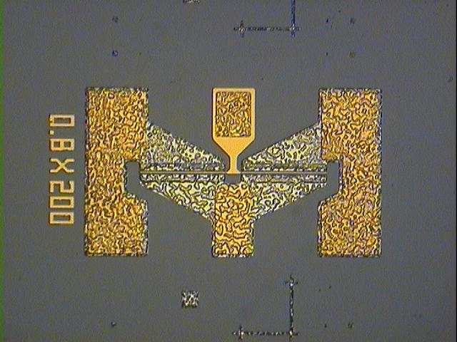
15 Metal contact failure mechanism Ni/Au gate on HEMT after thermal failure 100.0n 50.0n Using AES (area = micron to submicron) one can easily determine certain metal contact failure mechanisms. Example: Ni/Au gate contact The Ni diffuses to the surface, leaving Au in contact with the AlGaN. Current n n Voltage 25.0k 20.0k Ni Ga Fairly straight forward. Counts 15.0k 10.0k O Au Al 5.0k N Sputter cycles
16 Metal contact failure mechanism Failure of Ohmic contacts not as easily understood using AES. Using AES one cannot determine the bonding state of the element, only the amount and depth position. Example: A low resistivity ohmic contact is a blending of the different metals. Cannot determine if TiN interface formed. Must use XPS. Good Ohmic Contact (Ir based) Atomic Concentration (%) Atomic Concentration (%) Au Ir O Sputter Depth (Å) Ir-Control Al Ti Al O Ir Au Ti Ga Sputter Depth (Å) N Ir-900 o C Ga N
17 Identification of contamination Use of XPS can identify different sources of carbon contamination that are left behind from device processing. Characterization enhanced with UPS AES can only determine that C and O are present, but not the species or source. Counts/sec Counts/sec C 1s acetone ipa copolymer mibk ipa Binding energy (ev) O 1s acetone ipa copolymer mibk ipa Binding energy (ev)
18 XPS/UPS Projected Milestones Year 1- Characterize operational and failed devices in the mesa isolation region. Determine changes in surface chemistry and work function. Correlate chemical/electrical changes. Year 2- Design test structures to be placed in the die cut lines. Apply test structures to the cut lines and investigate variations in surface chemistry from post field stressing. Year 3- Design in-situ bias stressing fixture for XPS-UPS. Characterize cut line test structures under bias stress using XPS-UPS. Identify degradation mechanism. Investigate reactions of semiconductor/passivation interface. Year 4- Real-time observation of near-surface changes during bias stressing. Year 5- Small spot size XPS capability for direct analysis on die

19 Electrostatic force microscopy - EFM Scan area in AFM Tapping mode, then apply a bias to the tip and scan in EFM mode. tip Image of high aspect ratio EFM tip available from Veeco. EMF trace sample Veeco Dimension 3100 with Nanoscope V controller is currently installed in the MAIC facility

20 Electrostatic force microscopy - EFM Applied to pre and post aged devices to scan for variations of the electric field on the device surface. Examine defects propagating to the surface during testing, electromigration of gate metal in the gate-drain region, and increases in the surface potential from UV illumination emptying traps. Identify area for TEM/LEAP.
21 Electrostatic force microscopy - EFM Projected Milestones Year 1 Map the device surface of operational devices varying substrate bias and tip bias. Establish scan parameters for various compound semiconductor surfaces. Year 2 Map the device surface of failed devices and establish trends of failure in this region. Design probe cards for device biasing during scanning. Year 3 Correlate the failure mode to evolution of defects observed by TEM/LEAP. Incorporate defect generation and field profile into simulators. Year 4- Real-time imaging of devices during stressing Year 5-Establish limits of predictive forecast of reliability using short baisaging cycles.
22 xtra


23 High resolution XPS/UPS State of the art tools have <9um spot size and can build chemical maps of the surface Physical Electronics & Omicron High intensity monochromatic x-ray sources scan the surface. Sphera 60µm NanoESCA 650nm


24 Imaging Mode XPS/UPS Imaging at high kinetic electron energies. Ag evaporated on Cu, 35 µm field of view, 20 min acquisition time on Ag 3d5/2.


25 A 21st Century Approach to Reliability
X-Ray Photoelectron Spectroscopy (XPS) Prof. Paul K. Chu
 Prof. Paul K. Chu") X-Ray Photoelectron Spectroscopy (XPS) Prof. Paul K. Chu X-ray Photoelectron Spectroscopy Introduction Qualitative analysis Quantitative analysis Charging compensation Small area analysis and XPS imaging
X-Ray Photoelectron Spectroscopy (XPS) Prof. Paul K. Chu X-ray Photoelectron Spectroscopy Introduction Qualitative analysis Quantitative analysis Charging compensation Small area analysis and XPS imaging
Auger Electron Spectroscopy
 Auger Electron Spectroscopy Auger Electron Spectroscopy is an analytical technique that provides compositional information on the top few monolayers of material. Detect all elements above He Detection
Case Study of Electronic Materials Packaging with Poor Metal Adhesion and the Process for Performing Root Cause Failure Analysis
 Case Study of Electronic Materials Packaging with Poor Metal Adhesion and the Process for Performing Root Cause Failure Analysis Dr. E. A. Leone BACKGRUND ne trend in the electronic packaging industry
PHI 5000 Versaprobe-II Focus X-ray Photo-electron Spectroscopy
 PHI 5000 Versaprobe-II Focus X-ray Photo-electron Spectroscopy The very basic theory of XPS XPS theroy Surface Analysis Ultra High Vacuum (UHV) XPS Theory XPS = X-ray Photo-electron Spectroscopy X-ray
Electronic Supplementary Information. Molecular Antenna Tailored Organic Thin-film Transistor for. Sensing Application
 Electronic Supplementary Material (ESI) for Materials Horizons. This journal is The Royal Society of Chemistry 2017 Electronic Supplementary Information Molecular Antenna Tailored Organic Thin-film Transistor
Role of Electrochemical Reactions in the Degradation Mechanisms of AlGaN/GaN HEMTs
 Role of Electrochemical Reactions in the Degradation Mechanisms of AlGaN/GaN HEMTs Feng Gao 1,2, Bin Lu 2, Carl V. Thompson 1, Jesús del Alamo 2, Tomás Palacios 2 1. Department of Materials Science and
CVD-3 LFSIN SiN x Process
 CVD-3 LFSIN SiN x Process Top Electrode, C Bottom Electrode, C Pump to Base Time (s) SiH 4 Flow Standard LFSIN Process NH 3 Flow N 2 HF (watts) LF (watts) Pressure (mtorr Deposition Time min:s.s Pump to
CVD-3 MFSIN-HU-2 SiN x Mixed Frequency Process
 CVD-3 MFSIN-HU-2 SiN x Mixed Frequency Process Standard MFSIN-HU-2 Process Top C Bottom C Pump to Base Time (s) SiH 4 Flow HF/ LF NH 3 Flow HF/LF N 2 HF/LF HF (watts) LF (watts) HF Time LF Time Pressure
CVD-3 MFSIN-HU-1 SiN x Mixed Frequency Process
 CVD-3 MFSIN-HU-1 SiN x Mixed Frequency Process Standard MFSIN-HU-1 Process Top C Bottom C Pump to Base Time (s) SiH 4 Flow HF/ LF NH 3 Flow HF/LF N 2 HF/LF HF (watts) LF (watts) HF Time LF Time Pressure
Local Anodic Oxidation of GaAs: A Nanometer-Scale Spectroscopic Study with PEEM
 Local Anodic Oxidation of GaAs: A Nanometer-Scale Spectroscopic Study with PEEM S. Heun, G. Mori, M. Lazzarino, D. Ercolani, G. Biasiol, and L. Sorba Laboratorio TASC-INFM, 34012 Basovizza, Trieste A.
Characterization of Secondary Emission Materials for Micro-Channel Plates. S. Jokela, I. Veryovkin, A. Zinovev
 Characterization of Secondary Emission Materials for Micro-Channel Plates S. Jokela, I. Veryovkin, A. Zinovev Secondary Electron Yield Testing Technique We have incorporated XPS, UPS, Ar-ion sputtering,
Application of Surface Analysis for Root Cause Failure Analysis
 Application of Surface Analysis for Root Cause Failure Analysis David A. Cole Evans Analytical Group East Windsor, NJ Specialists in Materials Characterization Outline Introduction X-Ray Photoelectron
Spin-resolved photoelectron spectroscopy
 Spin-resolved photoelectron spectroscopy Application Notes Spin-resolved photoelectron spectroscopy experiments were performed in an experimental station consisting of an analysis and a preparation chamber.
Auger Electron Spectroscopy (AES)
") 1. Introduction Auger Electron Spectroscopy (AES) Silvia Natividad, Gabriel Gonzalez and Arena Holguin Auger Electron Spectroscopy (Auger spectroscopy or AES) was developed in the late 1960's, deriving
1. Introduction Auger Electron Spectroscopy (AES) Silvia Natividad, Gabriel Gonzalez and Arena Holguin Auger Electron Spectroscopy (Auger spectroscopy or AES) was developed in the late 1960's, deriving
Energy Spectroscopy. Ex.: Fe/MgO
 Energy Spectroscopy Spectroscopy gives access to the electronic properties (and thus chemistry, magnetism,..) of the investigated system with thickness dependence Ex.: Fe/MgO Fe O Mg Control of the oxidation
XPS & Scanning Auger Principles & Examples
 XPS & Scanning Auger Principles & Examples Shared Research Facilities Lunch Talk Contact info: dhu Pujari & Han Zuilhof Lab of rganic Chemistry Wageningen University E-mail: dharam.pujari@wur.nl Han.Zuilhof@wur.nl
Energy Spectroscopy. Excitation by means of a probe
 Energy Spectroscopy Excitation by means of a probe Energy spectral analysis of the in coming particles -> XAS or Energy spectral analysis of the out coming particles Different probes are possible: Auger
Effects of plasma treatment on the precipitation of fluorine-doped silicon oxide
 ARTICLE IN PRESS Journal of Physics and Chemistry of Solids 69 (2008) 555 560 www.elsevier.com/locate/jpcs Effects of plasma treatment on the precipitation of fluorine-doped silicon oxide Jun Wu a,, Ying-Lang
Introduction to X-ray Photoelectron Spectroscopy (XPS) XPS which makes use of the photoelectric effect, was developed in the mid-1960
 XPS which makes use of the photoelectric effect, was developed in the mid-1960") Introduction to X-ray Photoelectron Spectroscopy (XPS) X-ray Photoelectron Spectroscopy (XPS), also known as Electron Spectroscopy for Chemical Analysis (ESCA) is a widely used technique to investigate
Introduction to X-ray Photoelectron Spectroscopy (XPS) X-ray Photoelectron Spectroscopy (XPS), also known as Electron Spectroscopy for Chemical Analysis (ESCA) is a widely used technique to investigate
MSE 321 Structural Characterization
 Auger Spectroscopy Auger Electron Spectroscopy (AES) Scanning Auger Microscopy (SAM) Incident Electron Ejected Electron Auger Electron Initial State Intermediate State Final State Physical Electronics
CVD-3 SIO-HU SiO 2 Process
 CVD-3 SIO-HU SiO 2 Process Top Electrode, C Bottom Electrode, C Pump to Base Time (s) SiH 4 Flow Standard SIO-HU Process N 2 O Flow N 2 HF (watts) LF (watts) Pressure (mtorr Deposition Time min:s.s Pump
A DIVISION OF ULVAC-PHI
 A DIVISION OF ULVAC-PHI X-ray photoelectron spectroscopy (XPS/ESCA) is the most widely used surface analysis technique and has many well established industrial and research applications. XPS provides
Surface and Interface Characterization of Polymer Films
 Surface and Interface Characterization of Polymer Films Jeff Shallenberger, Evans Analytical Group 104 Windsor Center Dr., East Windsor NJ Copyright 2013 Evans Analytical Group Outline Introduction to
Normally-Off GaN Field Effect Power Transistors: Device Design and Process Technology Development
 Center for High Performance Power Electronics Normally-Off GaN Field Effect Power Transistors: Device Design and Process Technology Development Dr. Wu Lu (614-292-3462, lu.173@osu.edu) Dr. Siddharth Rajan
Nitride HFETs applications: Conductance DLTS
 Nitride HFETs applications: Conductance DLTS The capacitance DLTS cannot be used for device trap profiling as the capacitance for the gate will be very small Conductance DLTS is similar to capacitance
Traps in MOCVD n-gan Studied by Deep Level Transient Spectroscopy and Minority Carrier Transient Spectroscopy
 Traps in MOCVD n-gan Studied by Deep Level Transient Spectroscopy and Minority Carrier Transient Spectroscopy Yutaka Tokuda Department of Electrical and Electronics Engineering, Aichi Institute of Technology,
Lecture 5. X-ray Photoemission Spectroscopy (XPS)
") Lecture 5 X-ray Photoemission Spectroscopy (XPS) 5. Photoemission Spectroscopy (XPS) 5. Principles 5.2 Interpretation 5.3 Instrumentation 5.4 XPS vs UV Photoelectron Spectroscopy (UPS) 5.5 Auger Electron
Lecture 5 X-ray Photoemission Spectroscopy (XPS) 5. Photoemission Spectroscopy (XPS) 5. Principles 5.2 Interpretation 5.3 Instrumentation 5.4 XPS vs UV Photoelectron Spectroscopy (UPS) 5.5 Auger Electron
IV. Surface analysis for chemical state, chemical composition
 IV. Surface analysis for chemical state, chemical composition Probe beam Detect XPS Photon (X-ray) Photoelectron(core level electron) UPS Photon (UV) Photoelectron(valence level electron) AES electron
Plasma Deposition (Overview) Lecture 1
 Lecture 1") Plasma Deposition (Overview) Lecture 1 Material Processes Plasma Processing Plasma-assisted Deposition Implantation Surface Modification Development of Plasma-based processing Microelectronics needs (fabrication
Plasma Deposition (Overview) Lecture 1 Material Processes Plasma Processing Plasma-assisted Deposition Implantation Surface Modification Development of Plasma-based processing Microelectronics needs (fabrication
Sensors and Metrology. Outline
 Sensors and Metrology A Survey 1 Outline General Issues & the SIA Roadmap Post-Process Sensing (SEM/AFM, placement) In-Process (or potential in-process) Sensors temperature (pyrometry, thermocouples, acoustic
Photoemission Spectroscopy
 FY13 Experimental Physics - Auger Electron Spectroscopy Photoemission Spectroscopy Supervisor: Per Morgen SDU, Institute of Physics Campusvej 55 DK - 5250 Odense S Ulrik Robenhagen,
ToF-SIMS or XPS? Xinqi Chen Keck-II
 ToF-SIMS or XPS? Xinqi Chen Keck-II 1 Time of Flight Secondary Ion Mass Spectrometry (ToF-SIMS) Not ToF MS (laser, solution) X-ray Photoelectron Spectroscopy (XPS) 2 3 Modes of SIMS 4 Secondary Ion Sputtering
Photoelectron spectroscopy Instrumentation. Nanomaterials characterization 2
 Photoelectron spectroscopy Instrumentation Nanomaterials characterization 2 RNDr. Věra V Vodičkov ková,, PhD. Photoelectron Spectroscopy general scheme Impact of X-ray emitted from source to the sample
Reduced preferential sputtering of TiO 2 (and Ta 2 O 5 ) thin films through argon cluster ion bombardment.
 thin films through argon cluster ion bombardment.") NATIOMEM Reduced preferential sputtering of TiO 2 (and Ta 2 O 5 ) thin films through argon cluster ion bombardment. R. Grilli *, P. Mack, M.A. Baker * * University of Surrey, UK ThermoFisher Scientific
NATIOMEM Reduced preferential sputtering of TiO 2 (and Ta 2 O 5 ) thin films through argon cluster ion bombardment. R. Grilli *, P. Mack, M.A. Baker * * University of Surrey, UK ThermoFisher Scientific
The Use of Synchrotron Radiation in Modern Research
 The Use of Synchrotron Radiation in Modern Research Physics Chemistry Structural Biology Materials Science Geochemical and Environmental Science Atoms, molecules, liquids, solids. Electronic and geometric
Planar View of Structural Degradation in GaN HEMT: Voltage, Time and Temperature Dependence
 Planar View of Structural Degradation in GaN HEMT: Voltage, Time and Temperature Dependence Jungwoo Joh 1, Prashanth Makaram 2 Carl V. Thompson 2 and Jesús A. del Alamo 1 1 Microsystems Technology Laboratories,
Thermal measurement a requirement for monolithic microwave integrated circuit design
 Thermal measurement a requirement for monolithic microwave integrated circuit design Richard Hopper, Christopher Oxley Faculty of Computing Sciences and Engineering (CSE), De Montfort University, Leicester,
UVTOP265-HL-TO39. Description. Maximum Rating (T CASE = 25 C) Electro-Optical Characteristics (T CASE = 25 C, I F = 20 ma)
 Electro-Optical Characteristics (T CASE = 25 C, I F = 20 ma)") v3.0 05/17 UVTOP265-HL-TO39 Deep Ultraviolet Light Emission Source 270 nm, 0.6 mw TO39 Package Hemispherical Sapphire Lens Forensic Analysis, Disinfection Description UVTOP265-HL-TO39 is a deep ultraviolet
v3.0 05/17 UVTOP265-HL-TO39 Deep Ultraviolet Light Emission Source 270 nm, 0.6 mw TO39 Package Hemispherical Sapphire Lens Forensic Analysis, Disinfection Description UVTOP265-HL-TO39 is a deep ultraviolet
Auger Electron Spectroscopy (AES) Prof. Paul K. Chu
 Prof. Paul K. Chu") Auger Electron Spectroscopy (AES) Prof. Paul K. Chu Auger Electron Spectroscopy Introduction Principles Instrumentation Qualitative analysis Quantitative analysis Depth profiling Mapping Examples The Auger
Auger Electron Spectroscopy (AES) Prof. Paul K. Chu Auger Electron Spectroscopy Introduction Principles Instrumentation Qualitative analysis Quantitative analysis Depth profiling Mapping Examples The Auger
Self-study problems and questions Processing and Device Technology, FFF110/FYSD13
 Self-study problems and questions Processing and Device Technology, FFF110/FYSD13 Version 2016_01 In addition to the problems discussed at the seminars and at the lectures, you can use this set of problems
MSE 321 Structural Characterization
 Auger Spectroscopy Auger Electron Spectroscopy (AES) Scanning Auger Microscopy (SAM) Incident Electron Ejected Electron Auger Electron Initial State Intermediate State Final State Physical Electronics
Lecture 23 X-Ray & UV Techniques
 Lecture 23 X-Ray & UV Techniques Schroder: Chapter 11.3 1/50 Announcements Homework 6/6: Will be online on later today. Due Wednesday June 6th at 10:00am. I will return it at the final exam (14 th June).
DEPOSITION OF THIN TiO 2 FILMS BY DC MAGNETRON SPUTTERING METHOD
 Chapter 4 DEPOSITION OF THIN TiO 2 FILMS BY DC MAGNETRON SPUTTERING METHOD 4.1 INTRODUCTION Sputter deposition process is another old technique being used in modern semiconductor industries. Sputtering
Applications of XPS, AES, and TOF-SIMS
 Applications of XPS, AES, and TOF-SIMS Scott R. Bryan Physical Electronics 1 Materials Characterization Techniques Microscopy Optical Microscope SEM TEM STM SPM AFM Spectroscopy Energy Dispersive X-ray
MS482 Materials Characterization ( 재료분석 ) Lecture Note 12: Summary. Byungha Shin Dept. of MSE, KAIST
 Lecture Note 12: Summary. Byungha Shin Dept. of MSE, KAIST") 2015 Fall Semester MS482 Materials Characterization ( 재료분석 ) Lecture Note 12: Summary Byungha Shin Dept. of MSE, KAIST 1 Course Information Syllabus 1. Overview of various characterization techniques (1
2015 Fall Semester MS482 Materials Characterization ( 재료분석 ) Lecture Note 12: Summary Byungha Shin Dept. of MSE, KAIST 1 Course Information Syllabus 1. Overview of various characterization techniques (1
Multi-technique photoelectron spectrometer for micro-area spectroscopy and imaging
 Multi-technique photoelectron spectrometer for micro-area spectroscopy and imaging U. Manju, M. Sreemony and A. K. Chakraborty In this note we present the new multipurpose photoelectron spectroscopy facility
OFF-state TDDB in High-Voltage GaN MIS-HEMTs
 OFF-state TDDB in High-Voltage GaN MIS-HEMTs Shireen Warnock and Jesús A. del Alamo Microsystems Technology Laboratories (MTL) Massachusetts Institute of Technology (MIT) Purpose Further understanding
Birck Nanotechnology Center XPS: X-ray Photoelectron Spectroscopy ESCA: Electron Spectrometer for Chemical Analysis
 Birck Nanotechnology Center XPS: X-ray Photoelectron Spectroscopy ESCA: Electron Spectrometer for Chemical Analysis Dmitry Zemlyanov Birck Nanotechnology Center, Purdue University Outline Introduction
X-Ray Photoelectron Spectroscopy (XPS) Auger Electron Spectroscopy (AES)
 Auger Electron Spectroscopy (AES)") X-Ray Photoelectron Spectroscopy (XPS) Auger Electron Spectroscopy (AES) XPS X-ray photoelectron spectroscopy (XPS) is one of the most used techniques to chemically characterize the surface. Also known
X-Ray Photoelectron Spectroscopy (XPS) Auger Electron Spectroscopy (AES) XPS X-ray photoelectron spectroscopy (XPS) is one of the most used techniques to chemically characterize the surface. Also known
5) Surface photoelectron spectroscopy. For MChem, Spring, Dr. Qiao Chen (room 3R506) University of Sussex.
 Surface photoelectron spectroscopy. For MChem, Spring, Dr. Qiao Chen (room 3R506) University of Sussex.") For MChem, Spring, 2009 5) Surface photoelectron spectroscopy Dr. Qiao Chen (room 3R506) http://www.sussex.ac.uk/users/qc25/ University of Sussex Today s topics 1. Element analysis with XPS Binding energy,
For MChem, Spring, 2009 5) Surface photoelectron spectroscopy Dr. Qiao Chen (room 3R506) http://www.sussex.ac.uk/users/qc25/ University of Sussex Today s topics 1. Element analysis with XPS Binding energy,
Advanced Lab Course. X-Ray Photoelectron Spectroscopy 1 INTRODUCTION 1 2 BASICS 1 3 EXPERIMENT Qualitative analysis Chemical Shifts 7
 Advanced Lab Course X-Ray Photoelectron Spectroscopy M210 As of: 2015-04-01 Aim: Chemical analysis of surfaces. Content 1 INTRODUCTION 1 2 BASICS 1 3 EXPERIMENT 3 3.1 Qualitative analysis 6 3.2 Chemical
The design of an integrated XPS/Raman spectroscopy instrument for co-incident analysis
 The design of an integrated XPS/Raman spectroscopy instrument for co-incident analysis Tim Nunney The world leader in serving science 2 XPS Surface Analysis XPS +... UV Photoelectron Spectroscopy UPS He(I)
MS482 Materials Characterization ( 재료분석 ) Lecture Note 4: XRF
 Lecture Note 4: XRF") 2016 Fall Semester MS482 Materials Characterization ( 재료분석 ) Lecture Note 4: XRF Byungha Shin Dept. of MSE, KAIST 1 Course Information Syllabus 1. Overview of various characterization techniques (1 lecture)
2016 Fall Semester MS482 Materials Characterization ( 재료분석 ) Lecture Note 4: XRF Byungha Shin Dept. of MSE, KAIST 1 Course Information Syllabus 1. Overview of various characterization techniques (1 lecture)
Methods of surface analysis
 Methods of surface analysis Nanomaterials characterisation I RNDr. Věra Vodičková, PhD. Surface of solid matter: last monoatomic layer + absorbed monolayer physical properties are effected (crystal lattice
QUESTIONS AND ANSWERS
 QUESTIONS AND ANSWERS (1) For a ground - state neutral atom with 13 protons, describe (a) Which element this is (b) The quantum numbers, n, and l of the inner two core electrons (c) The stationary state
Atomic Level Analysis of SiC Devices Using Numerical Simulation
 Atomic Level Analysis of Devices Using Numerical mulation HIRSE, Takayuki MRI, Daisuke TERA, Yutaka ABSTRAT Research and development of power semiconductor devices with (silicon carbide) has been very
Supporting Data. The University of Texas at Dallas, 800 West Campbell Road, Richardson, Texas 75080, United
 Supporting Data MoS 2 Functionalization for Ultra-thin Atomic Layer Deposited Dielectrics Angelica Azcatl, 1 Stephen McDonnell, 1 Santosh KC, 1 Xing Peng, 1 Hong Dong, 1 Xiaoye Qin, 1 Rafik Addou, 1 Greg
Strain and Temperature Dependence of Defect Formation at AlGaN/GaN High Electron Mobility Transistors on a Nanometer Scale
 Strain and Temperature Dependence of Defect Formation at AlGaN/GaN High Electron Mobility Transistors on a Nanometer Scale Chung-Han Lin Department of Electrical & Computer Engineering, The Ohio State
2) Atom manipulation. Xe / Ni(110) Model: Experiment:
 Atom manipulation. Xe / Ni(110) Model: Experiment:") 2) Atom manipulation D. Eigler & E. Schweizer, Nature 344, 524 (1990) Xe / Ni(110) Model: Experiment: G.Meyer, et al. Applied Physics A 68, 125 (1999) First the tip is approached close to the adsorbate
2) Atom manipulation D. Eigler & E. Schweizer, Nature 344, 524 (1990) Xe / Ni(110) Model: Experiment: G.Meyer, et al. Applied Physics A 68, 125 (1999) First the tip is approached close to the adsorbate
Local Anodic Oxidation with AFM: A Nanometer-Scale Spectroscopic Study with Photoemission Microscopy
 Local Anodic Oxidation with AFM: A Nanometer-Scale Spectroscopic Study with Photoemission Microscopy S. Heun, G. Mori, M. Lazzarino, D. Ercolani,* G. Biasiol, and L. Sorba* Laboratorio Nazionale TASC-INFM,
X-ray Photoelectron Spectroscopy (XPS)
") X-ray Photoelectron Spectroscopy (XPS) As part of the course Characterization of Catalysts and Surfaces Prof. Dr. Markus Ammann Paul Scherrer Institut markus.ammann@psi.ch Resource for further reading:
X-ray Photoelectron Spectroscopy (XPS) As part of the course Characterization of Catalysts and Surfaces Prof. Dr. Markus Ammann Paul Scherrer Institut markus.ammann@psi.ch Resource for further reading:
(a) (b) Supplementary Figure 1. (a) (b) (a) Supplementary Figure 2. (a) (b) (c) (d) (e)
 (b) Supplementary Figure 1. (a) (b) (a) Supplementary Figure 2. (a) (b) (c) (d) (e)") (a) (b) Supplementary Figure 1. (a) An AFM image of the device after the formation of the contact electrodes and the top gate dielectric Al 2 O 3. (b) A line scan performed along the white dashed line
(a) (b) Supplementary Figure 1. (a) An AFM image of the device after the formation of the contact electrodes and the top gate dielectric Al 2 O 3. (b) A line scan performed along the white dashed line
A HYDROGEN SENSITIVE Pd/GaN SCHOTTKY DIODE SENSOR
 Journal of Physical Science, Vol. 17(2), 161 167, 2006 161 A HYDROGEN SENSITIVE Pd/GaN SCHOTTKY DIODE SENSOR A.Y. Hudeish 1,2* and A. Abdul Aziz 1 1 School of Physics, Universiti Sains Malaysia, 11800
Supplementary Figure 1. Visible (λ = 633 nm) Raman spectra of a-co x layers. (a) Raman spectra of
 Raman spectra of a-co x layers. (a) Raman spectra of") a In te n s ity [a.u.] c In te n s ity [a.u.] 6 4 2 4 3 2 1 3 2.5 2 1.5 1 p O 2 3.5 1,5 3, 4,5 R a m a n s h ift [c m -1 ] p ris tin e 1 o C 2 o C 3 o C 4 o C 5 o C b d In te n s ity [a.u.] In te n s ity
a In te n s ity [a.u.] c In te n s ity [a.u.] 6 4 2 4 3 2 1 3 2.5 2 1.5 1 p O 2 3.5 1,5 3, 4,5 R a m a n s h ift [c m -1 ] p ris tin e 1 o C 2 o C 3 o C 4 o C 5 o C b d In te n s ity [a.u.] In te n s ity
DISTRIBUTION OF POTENTIAL BARRIER HEIGHT LOCAL VALUES AT Al-SiO 2 AND Si-SiO 2 INTERFACES OF THE METAL-OXIDE-SEMICONDUCTOR (MOS) STRUCTURES
 STRUCTURES") DISTRIBUTION OF POTENTIAL BARRIER HEIGHT LOCAL VALUES AT Al-SiO 2 AND Si-SiO 2 INTERFACES OF THE ETAL-OXIDE-SEICONDUCTOR (OS) STRUCTURES KRZYSZTOF PISKORSKI (kpisk@ite.waw.pl), HENRYK. PRZEWLOCKI Institute
DISTRIBUTION OF POTENTIAL BARRIER HEIGHT LOCAL VALUES AT Al-SiO 2 AND Si-SiO 2 INTERFACES OF THE ETAL-OXIDE-SEICONDUCTOR (OS) STRUCTURES KRZYSZTOF PISKORSKI (kpisk@ite.waw.pl), HENRYK. PRZEWLOCKI Institute
raw materials C V Mn Mg S Al Ca Ti Cr Si G H Nb Na Zn Ni K Co A B C D E F
 Today s advanced batteries require a range of specialized analytical tools to better understand the electrochemical processes that occur during battery cycling. Evans Analytical Group (EAG) offers a wide-range
structure and paramagnetic character R. Kakavandi, S-A. Savu, A. Caneschi, T. Chassé, M. B. Casu Electronic Supporting Information
 At the interface between organic radicals and TiO 2 (110) single crystals: electronic structure and paramagnetic character R. Kakavandi, S-A. Savu, A. Caneschi, T. Chassé, M. B. Casu Electronic Supporting
Quality and Reliability Report
 Quality and Reliability Report GaAs Schottky Diode Products 051-06444 rev C Marki Microwave Inc. 215 Vineyard Court, Morgan Hill, CA 95037 Phone: (408) 778-4200 / FAX: (408) 778-4300 Email: info@markimicrowave.com
Focused Ion Beam Induced Local Tungsten Deposition
 Focused Ion Beam Induced Local Tungsten Deposition H. Langfischer, B. Basnar, E. Bertagnolli Institute for Solid State Electronics, Vienna University of Technology, Floragasse 7, 1040 ien, Austria H. Hutter
Electron Microprobe Analysis 1 Nilanjan Chatterjee, Ph.D. Principal Research Scientist
 12.141 Electron Microprobe Analysis 1 Nilanjan Chatterjee, Ph.D. Principal Research Scientist Massachusetts Institute of Technology Electron Microprobe Facility Department of Earth, Atmospheric and Planetary
PHOTOELECTRON SPECTROSCOPY IN AIR (PESA)
") PHOTOELECTRON SPECTROSCOPY IN AIR (PESA) LEADERS IN GAS DETECTION Since 1977 Model AC-3 Features: Atmospheric pressure operation (unique in the world) Estimate work function, ionization potential, density
PHOTOELECTRON SPECTROSCOPY IN AIR (PESA) LEADERS IN GAS DETECTION Since 1977 Model AC-3 Features: Atmospheric pressure operation (unique in the world) Estimate work function, ionization potential, density
Electron Microprobe Analysis 1 Nilanjan Chatterjee, Ph.D. Principal Research Scientist
 12.141 Electron Microprobe Analysis 1 Nilanjan Chatterjee, Ph.D. Principal Research Scientist Massachusetts Institute of Technology Electron Microprobe Facility Department of Earth, Atmospheric and Planetary
Cho Fai Jonathan Lau, Xiaofan Deng, Qingshan Ma, Jianghui Zheng, Jae S. Yun, Martin A.
 Supporting Information CsPbIBr 2 Perovskite Solar Cell by Spray Assisted Deposition Cho Fai Jonathan Lau, Xiaofan Deng, Qingshan Ma, Jianghui Zheng, Jae S. Yun, Martin A. Green, Shujuan Huang, Anita W.
Self-Assembled InAs Quantum Dots
 Self-Assembled InAs Quantum Dots Steve Lyon Department of Electrical Engineering What are semiconductors What are semiconductor quantum dots How do we make (grow) InAs dots What are some of the properties
The Benefit of Wide Energy Range Spectrum Acquisition During Sputter Depth Profile Measurements
 The Benefit of Wide Energy Range Spectrum Acquisition During Sputter Depth Profile Measurements Uwe Scheithauer, 82008 Unterhaching, Germany E-Mail: scht.uhg@googlemail.com Internet: orcid.org/0000-0002-4776-0678;
Magnetic Force Microscopy (MFM) F = µ o (m )H
 F = µ o (m )H") Magnetic Force Microscopy (MFM) F = µ o (m )H 1. MFM is based on the use of a ferromagnetic tip as a local field sensor. Magnetic interaction between the tip and the surface results in a force acting on
Magnetic Force Microscopy (MFM) F = µ o (m )H 1. MFM is based on the use of a ferromagnetic tip as a local field sensor. Magnetic interaction between the tip and the surface results in a force acting on
Removal of Cu Impurities on a Si Substrate by Using (H 2 O 2 +HF) and (UV/O 3 +HF)
 and (UV/O 3 +HF)") Journal of the Korean Physical Society, Vol. 33, No. 5, November 1998, pp. 579 583 Removal of Cu Impurities on a Si Substrate by Using (H 2 O 2 +HF) and (UV/O 3 +HF) Baikil Choi and Hyeongtag Jeon School
Journal of the Korean Physical Society, Vol. 33, No. 5, November 1998, pp. 579 583 Removal of Cu Impurities on a Si Substrate by Using (H 2 O 2 +HF) and (UV/O 3 +HF) Baikil Choi and Hyeongtag Jeon School
MS482 Materials Characterization ( 재료분석 ) Lecture Note 2: UPS
 Lecture Note 2: UPS") 2016 Fall Semester MS482 Materials Characterization ( 재료분석 ) Lecture Note 2: UPS Byungha Shin Dept. of MSE, KAIST 1 Course Information Syllabus 1. Overview of various characterization techniques (1 lecture)
2016 Fall Semester MS482 Materials Characterization ( 재료분석 ) Lecture Note 2: UPS Byungha Shin Dept. of MSE, KAIST 1 Course Information Syllabus 1. Overview of various characterization techniques (1 lecture)
Electron Rutherford Backscattering, a versatile tool for the study of thin films
 Electron Rutherford Backscattering, a versatile tool for the study of thin films Maarten Vos Research School of Physics and Engineering Australian National University Canberra Australia Acknowledgements:
Surface Sensitivity & Surface Specificity
 Surface Sensitivity & Surface Specificity The problems of sensitivity and detection limits are common to all forms of spectroscopy. In its simplest form, the question of sensitivity boils down to whether
Nanostructure. Materials Growth Characterization Fabrication. More see Waser, chapter 2
 Nanostructure Materials Growth Characterization Fabrication More see Waser, chapter 2 Materials growth - deposition deposition gas solid Physical Vapor Deposition Chemical Vapor Deposition Physical Vapor
Processing and Characterization of GaSb/High-k Dielectric Interfaces. Pennsylvania 16802, USA. University Park, Pennsylvania 16802, USA
 10.1149/1.3630839 The Electrochemical Society Processing and Characterization of GaSb/High-k Dielectric Interfaces E. Hwang a, C. Eaton b, S. Mujumdar a, H. Madan a, A. Ali a, D. Bhatia b, S. Datta a and
Theory of Electrical Characterization of Semiconductors
 Theory of Electrical Characterization of Semiconductors P. Stallinga Universidade do Algarve U.C.E.H. A.D.E.E.C. OptoElectronics SELOA Summer School May 2000, Bologna (It) Overview Devices: bulk Schottky
Imaging Methods: Scanning Force Microscopy (SFM / AFM)
") Imaging Methods: Scanning Force Microscopy (SFM / AFM) The atomic force microscope (AFM) probes the surface of a sample with a sharp tip, a couple of microns long and often less than 100 Å in diameter.
Imaging Methods: Scanning Force Microscopy (SFM / AFM) The atomic force microscope (AFM) probes the surface of a sample with a sharp tip, a couple of microns long and often less than 100 Å in diameter.
PHOTOELECTRON SPECTROSCOPY (PES)
") PHOTOELECTRON SPECTROSCOPY (PES) NTRODUCTON Law of Photoelectric effect Albert Einstein, Nobel Prize 1921 Kaiser-Wilhelm-nstitut (now Max-Planck- nstitut) für Physik Berlin, Germany High-resolution electron
PHOTOELECTRON SPECTROSCOPY (PES) NTRODUCTON Law of Photoelectric effect Albert Einstein, Nobel Prize 1921 Kaiser-Wilhelm-nstitut (now Max-Planck- nstitut) für Physik Berlin, Germany High-resolution electron
Secondaryionmassspectrometry
 Secondaryionmassspectrometry (SIMS) 1 Incident Ion Techniques for Surface Composition Analysis Mass spectrometric technique 1. Ionization -Electron ionization (EI) -Chemical ionization (CI) -Field ionization
Defense Technical Information Center Compilation Part Notice
 UNCLASSIFIED Defense Technical Information Center Compilation Part Notice ADP013351 TITLE: The Effects of Plasma Induced Damage on the Channel Layers of Ion Implanted GaAs MESFETs during Reactive Ion Etching
Solid State Detectors
 Solid State Detectors Most material is taken from lectures by Michael Moll/CERN and Daniela Bortoletto/Purdue and the book Semiconductor Radiation Detectors by Gerhard Lutz. In gaseous detectors, a charged
Auger Electron Spectroscopy Overview
 Auger Electron Spectroscopy Overview Also known as: AES, Auger, SAM 1 Auger Electron Spectroscopy E KLL = E K - E L - E L AES Spectra of Cu EdN(E)/dE Auger Electron E N(E) x 5 E KLL Cu MNN Cu LMM E f E
4FNJDPOEVDUPS 'BCSJDBUJPO &UDI
 2010.5.4 1 Major Fabrication Steps in CMOS Process Flow UV light oxygen Silicon dioxide Silicon substrate Oxidation (Field oxide) photoresist Photoresist Coating Mask exposed photoresist Mask-Wafer Exposed
Spatially resolving density-dependent screening around a single charged atom in graphene
 Supplementary Information for Spatially resolving density-dependent screening around a single charged atom in graphene Dillon Wong, Fabiano Corsetti, Yang Wang, Victor W. Brar, Hsin-Zon Tsai, Qiong Wu,
X- ray Photoelectron Spectroscopy and its application in phase- switching device study
 X- ray Photoelectron Spectroscopy and its application in phase- switching device study Xinyuan Wang A53073806 I. Background X- ray photoelectron spectroscopy is of great importance in modern chemical and
Surface Defects on Natural MoS 2
 Supporting Information: Surface Defects on Natural MoS 2 Rafik Addou 1*, Luigi Colombo 2, and Robert M. Wallace 1* 1 Department of Materials Science and Engineering, The University of Texas at Dallas,
X-Ray Photoelectron Spectroscopy (XPS)
") X-Ray Photoelectron Spectroscopy (XPS) Louis Scudiero http://www.wsu.edu/~scudiero; 5-2669 Fulmer 261A Electron Spectroscopy for Chemical Analysis (ESCA) The basic principle of the photoelectric effect
X-Ray Photoelectron Spectroscopy (XPS) Louis Scudiero http://www.wsu.edu/~scudiero; 5-2669 Fulmer 261A Electron Spectroscopy for Chemical Analysis (ESCA) The basic principle of the photoelectric effect
An Introduction to Auger Electron Spectroscopy
 An Introduction to Auger Electron Spectroscopy Spyros Diplas MENA3100 SINTEF Materials & Chemistry, Department of Materials Physics & Centre of Materials Science and Nanotechnology, Department of Chemistry,
Table 1: Residence time (τ) in seconds for adsorbed molecules
 in seconds for adsorbed molecules") 1 Surfaces We got our first hint of the importance of surface processes in the mass spectrum of a high vacuum environment. The spectrum was dominated by water and carbon monoxide, species that represent
1 Surfaces We got our first hint of the importance of surface processes in the mass spectrum of a high vacuum environment. The spectrum was dominated by water and carbon monoxide, species that represent
Supporting Information s for
 Supporting Information s for # Self-assembling of DNA-templated Au Nanoparticles into Nanowires and their enhanced SERS and Catalytic Applications Subrata Kundu* and M. Jayachandran Electrochemical Materials
MS482 Materials Characterization ( 재료분석 ) Lecture Note 5: RBS
 Lecture Note 5: RBS") 2016 Fall Semester MS482 Materials Characterization ( 재료분석 ) Lecture Note 5: RBS Byungha Shin Dept. of MSE, KAIST 1 Course Information Syllabus 1. Overview of various characterization techniques (1 lecture)
2016 Fall Semester MS482 Materials Characterization ( 재료분석 ) Lecture Note 5: RBS Byungha Shin Dept. of MSE, KAIST 1 Course Information Syllabus 1. Overview of various characterization techniques (1 lecture)
Etching Issues - Anisotropy. Dry Etching. Dry Etching Overview. Etching Issues - Selectivity
 Etching Issues - Anisotropy Dry Etching Dr. Bruce K. Gale Fundamentals of Micromachining BIOEN 6421 EL EN 5221 and 6221 ME EN 5960 and 6960 Isotropic etchants etch at the same rate in every direction mask
Auger Electron Spectroscopy *
 OpenStax-CNX module: m43546 1 Auger Electron Spectroscopy * Amanda M. Goodman Andrew R. Barron This work is produced by OpenStax-CNX and licensed under the Creative Commons Attribution License 3.0 1 Basic