Large Area Plasmonic Color Palettes with Expanded Gamut Using. Colloidal Self-Assembly
|
|
|
- Jasper York
- 5 years ago
- Views:
Transcription
1 Large Area Plasmonic Color Palettes with Expanded Gamut Using Colloidal Self-Assembly Liancheng Wang 1, Ray J. H. Ng 1, Saman Safari Dinachali 1, Mahsa Jalali 1, Ye Yu 1, and Joel K.W. Yang 1,2 1 Engineering Product Development Pillar (EPD), Singapore University of Technology & Design, 8 Somapah Road, Singapore Institute of Materials Research and Engineering (IMRE), A*STAR, 2 Fusionopolis Way. Innovis, Singapore KEYWORDS: Plasmonic color; Aluminium; Polystyrene; Colloidal Self-assembly; 1. PS shrinkage and HSQ etching Surface irregularities and roughness appeared when the particles were etched to around half of their original size, as shown in the bottom part in Fig. S1a). Even when deformed, the PS particles were still capable of serving as the DRIE etch mask, but the surface roughness was transferred to the underlying HSQ posts (Fig. S1b). With further size reduction, the integrity of the PS particles as an etch mask is severely reduced. In this paper, we investigated only colors arising from particles with diameter to pitch ratios greater than 1:5 (Fig. S1b).
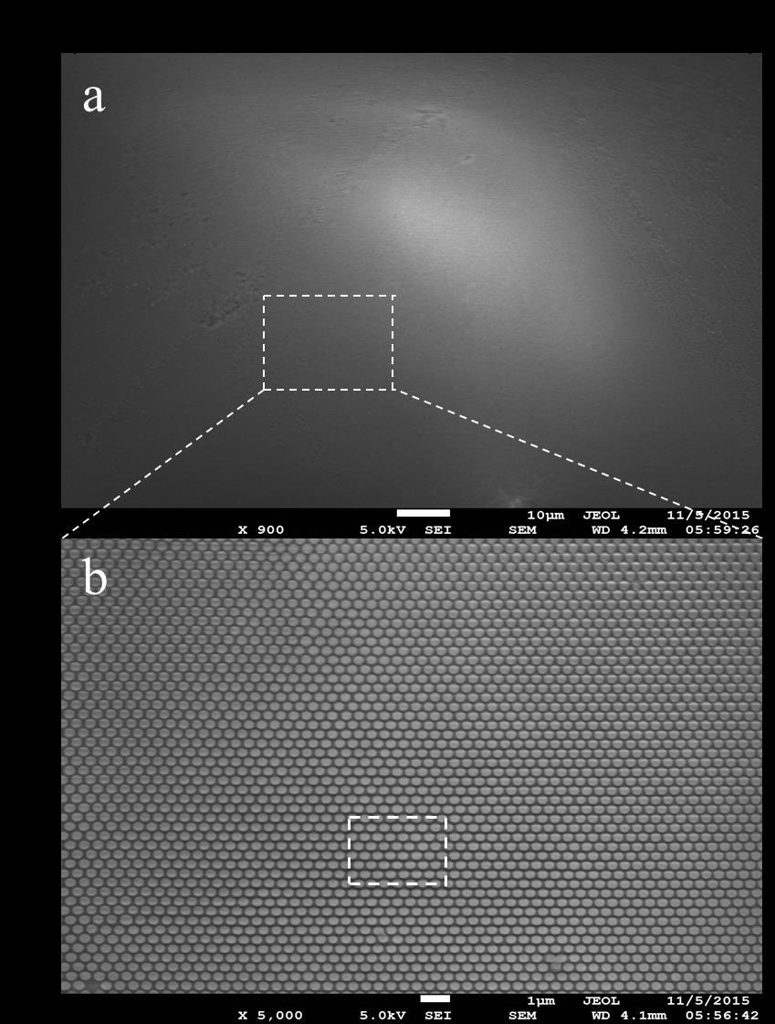
 with long range order over 120μm by 100μm. Figure S2(b) is a magnified view of the dashed box in Fig. S2(a) while Fig.")
2 Fig. S1 2. Long-range order of our proposed process Our proposed process shows high efficiency and cost-effectiveness, and yields structures with high uniformity over a large area. Figure S2 shows the structure of Al Disks (P=420nm, R=150nm) with long range order over 120μm by 100μm. Figure S2(b) is a magnified view of the dashed box in Fig. S2(a) while Fig. S2(c) is a magnification of the dashed box in Fig. S2(b).
3

 with varying HSQ heights of 60nm")
4 Fig. S2 3. Al disks with varying HSQ height Figure S3 shows the structures of Al disks (P=420nm, R=150nm) with varying HSQ heights of 60nm (a), 90nm (b) and 120nm (c). Fig. S3
5 4. Discussion and analysis of the resonances modes-al Disks To understand the underlying mechanism governing the reflectance response of Al Disks, we overlay the respective reflectance curves obtained from the corresponding FDTD simulations, as presented in Fig. S4.1. Figure 4.2 shows the spectra of the Al Disks with varying R, P and H. Figure. S4.1(a) shows the color contour plot of the reflectance spectra with varying R and fixed P,H=420nm, 100nm. Three bands of reflectance dip, A, B, C are clearly observed in Fig. S4.1(a). Band_A stays constant at λ~360nm with the narrowest FWHM of ~30nm, which is related to the lattice diffraction. Band_B is related to the high order mode, which overlaps with band_a when R is below 90nm, but further redshifts, intensifies and widens when R increases, to λ=~556nm when R=180nm. It was also found that, when R is small (i.e., R=60nm), the back reflector tends to increase the reflectance intensity. However, when R is large, the intensification effect of the back reflector Al weakens and the spectrum of the Al Disks evolves to quite resemble that of the structure without the back reflector. Band_C is caused by the fundamental mode, which is dominant when R is small. For the previous reported plasmonic structure, the fundamental mode is the dominant mode responsible for color generation in the visible range. The fundamental mode broadens and redshifts significantly, and moves out of the visible region when R is larger than 120nm. From Fig. S4.2, we noticed that, for the 420nm-pitch Al Disks, when R is large, band_a and band_b contribute together to filter the incidence, whereas the fundamental mode dominates when R is small. The diverse combination of these resonances when R varies produces color spanning from pink to yellow, green and blue. For the 628nm and 520nmpitch based Al Disks, the high order mode, i.e. band_b, which dominates the spectra, is
6 located at the yellow red region, producing a bluish color. We further examined the electric field intensity distribution through a vertical cross section of the Al Disks, as shown in Fig. S4.1 (b). Figure S4.1 (a2) shows the 2D color map of the reflectance intensity as a function of pitch, with fixed R=100 and H=100nm. The diffraction mode redshifts when P increases, as governed by the dispersion characteristics of SPR. Similarly, when R/P ratio is large, the spectra are dominant by the top disks and HSQ posts in Al Disks. Figure S4.1(a3) and (a4) are 2D color maps with varied H and fixed (a3): P, R=(420, 80nm) and (a4) P, R=(420, 150nm), respectively. In Fig. S4.1(a3), for small R (80nm), when H increases, the fundamental mode blueshifts from 500nm to 700nm since the mode energy increases. When R is large (150nm) (Fig. S4.1 (a4)), the high order mode dominates due to the large size of the disks. The high order mode redshifts from 448nm (H=60nm) to 527nm (H=150nm). Our theoretical assessment here provides a good understanding of the mechanism governing the plasmonic color generation, thus it could further facilitate the design of plasmonic coloration structure.

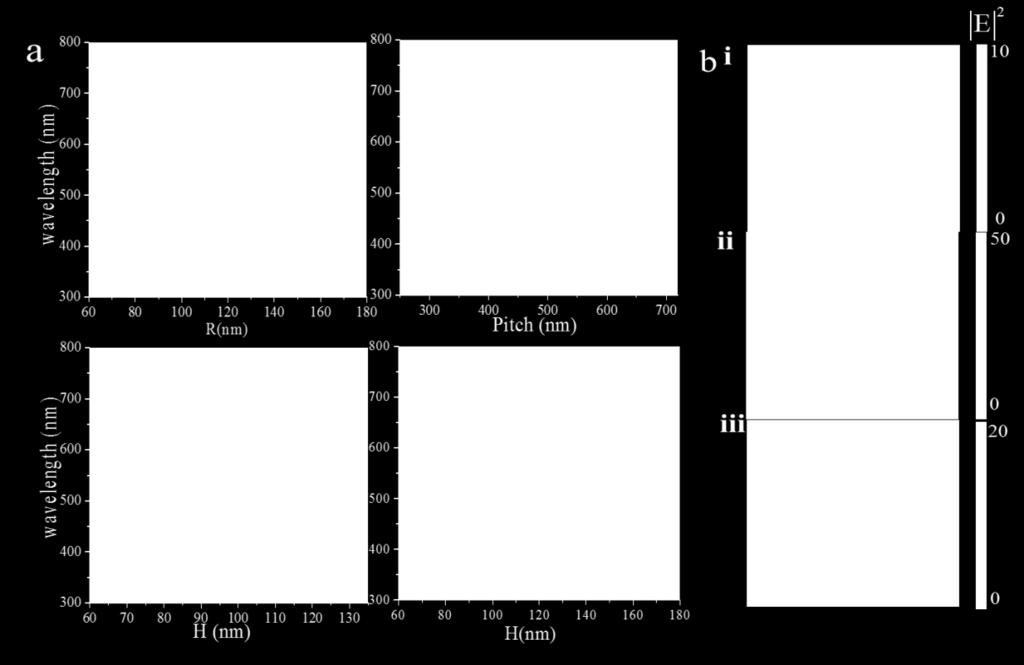
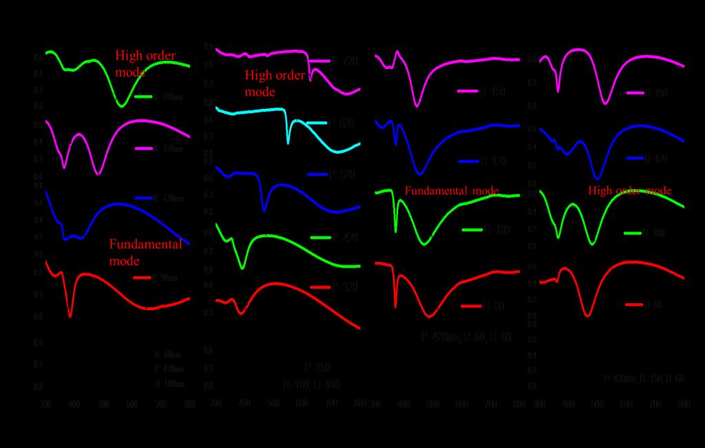
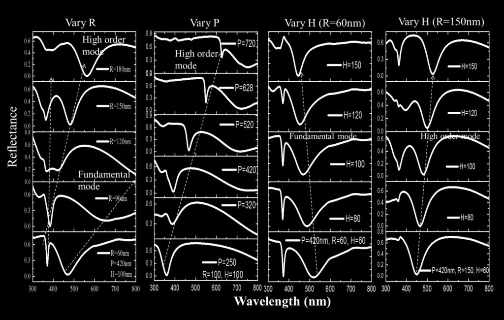
7 Fig. S 4.1 Fig. S 4.2

 plots the electric field distribution in the cross section plane and transverse plane of the modes in Al Rings, denoted in Fig. S6 (a).")
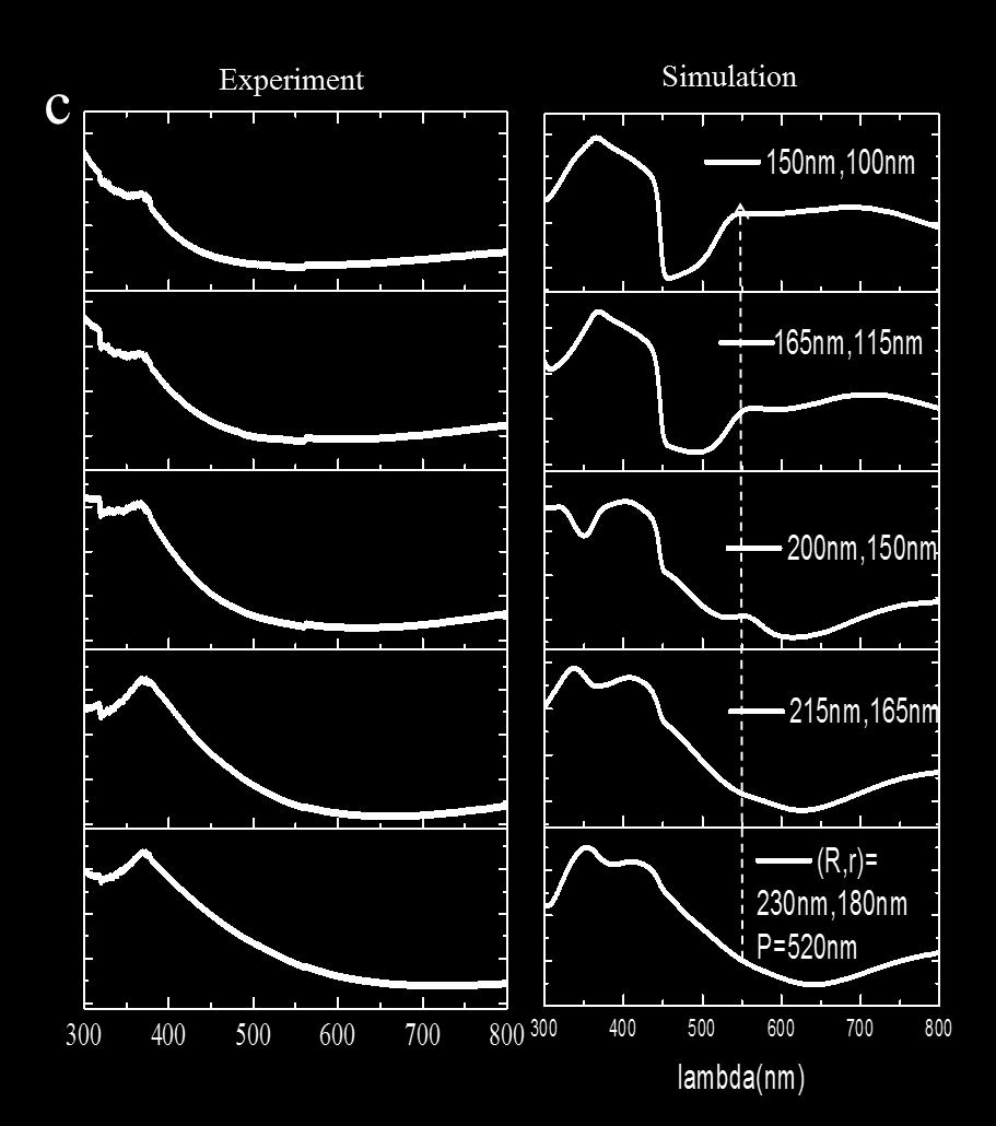
8 5. Discussion and analysis of the resonances modes-al Dome-Rings For the Al Dome-Rings, we confirmed the localized modes and various hybrid modes from the electric field distribution based on FDTD simulation. Various modes arise from the interaction of various localized modes supported by the dome and the plasmonic modes in the rings, as shown in Fig. S5. Fig. S 5 6. Discussion and analysis of the resonances modes-al Rings Figure S6 (a) shows the simulated spectra of Al Rings with varying outer and inner radii (R, r) with fixed pitch of 420nm, and Fig. S6(b) plots the electric field distribution in the cross section plane and transverse plane of the modes in Al Rings, denoted in Fig. S6 (a). The mode i shows a relatively wider FWHM (due to large radiative loss). Mode i redshifts when the inner radius r increases and the outer radius R is fixed due to increased circumferential length of the ring. The electric field of the mode ii is mostly confined at the rim of the outer radius and the gap between the neighbouring rings. Mode ii remains almost invariant when R is fixed and r is varied, and redshifts when R increases. This is because the circumferential length of the ring increases and the

 further re-plots the experimental curves in Fig.")
9 gap between the neighbouring rings narrows (resulting in a lower energy stored in the rings). Mode iii blueshifts when R is fixed and r is decreased, due to a decreased width of the ring. The dip iv corresponds to the Bragg diffractive mode, which remains invariant at ~λ= 365nm for the 420nm-pitch Al Rings. Mode v corresponds to a high order modes. Figure S6 (c) further re-plots the experimental curves in Fig. 4 (a-iv) and the corresponding simulation results, which are similar to each other. Fig. S 6 (a) and (b)
")
10 Fig. S 6 (c)
Supporting information. Unidirectional Doubly Enhanced MoS 2 Emission via
 Supporting information Unidirectional Doubly Enhanced MoS 2 Emission via Photonic Fano Resonances Xingwang Zhang, Shinhyuk Choi, Dake Wang, Carl H. Naylor, A. T. Charlie Johnson, and Ertugrul Cubukcu,,*
Superlattice Plasmons in Hierarchical Au Nanoparticle Arrays
 SUPPLEMENTAL INFORMATION Superlattice Plasmons in Hierarchical Au Nanoparticle Arrays Danqing Wang 1, Ankun Yang 2, Alexander J. Hryn 2, George C. Schatz 1,3 and Teri W. Odom 1,2,3 1 Graduate Program in
Symmetry Breaking in Oligomer Surface Plasmon Lattice Resonances
 Supporting Information Symmetry Breaking in Oligomer Surface Plasmon Lattice Resonances Marco Esposito 1, Francesco Todisco 2, Said Bakhti 3, Adriana Passaseo* 1, Iolena Tarantini 4, Massimo Cuscunà 1,
Accurate Modeling of Dark-Field Scattering Spectra
 Accurate Modeling of Dark-Field Scattering Spectra of Plasmonic Nanostructures (Supporting Information) Liyong Jiang 1,2,, Tingting Yin 2,, Zhaogang Dong 3,, Mingyi Liao 4, Shawn J. Tan 3, Xiao Ming Goh
Printing Colour at the Optical Diffraction Limit
 SUPPLEMENTARY INFORMATION DOI: 10.1038/NNANO.2012.128 Printing Colour at the Optical Diffraction Limit Karthik Kumar 1,#, Huigao Duan 1,#, Ravi S. Hegde 2, Samuel C.W. Koh 1, Jennifer N. Wei 1 and Joel
Photonic crystals. Semi-conductor crystals for light. The smallest dielectric lossless structures to control whereto and how fast light flows
 Photonic crystals Semi-conductor crystals for light The smallest dielectric lossless structures to control whereto and how fast light flows Femius Koenderink Center for Nanophotonics AMOLF, Amsterdam f.koenderink@amolf.nl
Optical cavity modes in gold shell particles
 9 Optical cavity modes in gold shell particles Gold (Au) shell particles with dimensions comparable to the wavelength of light exhibit a special resonance, with a tenfold field enhancement over almost
Supporting Information. Direct n- to p-type Channel Conversion in Monolayer/Few-Layer WS 2 Field-Effect Transistors by Atomic Nitrogen Treatment
 Supporting Information Direct n- to p-type Channel Conversion in Monolayer/Few-Layer WS 2 Field-Effect Transistors by Atomic Nitrogen Treatment Baoshan Tang 1,2,, Zhi Gen Yu 3,, Li Huang 4, Jianwei Chai
Supplementary Figure S1 SEM and optical images of Si 0.6 H 0.4 colloids. a, SEM image of Si 0.6 H 0.4 colloids. b, The size distribution of Si 0.
 Supplementary Figure S1 SEM and optical images of Si 0.6 H 0.4 colloids. a, SEM image of Si 0.6 H 0.4 colloids. b, The size distribution of Si 0.6 H 0.4 colloids. The standard derivation is 4.4 %. Supplementary
Optical properties of spherical and anisotropic gold shell colloids
 8 Optical properties of spherical and anisotropic gold shell colloids Core/shell colloids consisting of a metal shell and a dielectric core are known for their special optical properties. The surface plasmon
Graphene Helicoid: The Distinct Properties Promote Application of Graphene Related Materials in Thermal Management
 Supporting Information Graphene Helicoid: The Distinct Properties Promote Application of Graphene Related Materials in Thermal Management Haifei Zhan 1,2, Gang Zhang 3,*, Chunhui Yang 1, and Yuantong Gu
Electronic Supplementary Information (ESI) for. Engineering nanoscale p-n junction via the synergetic dual-doping of p-type boron-doped
 for. Engineering nanoscale p-n junction via the synergetic dual-doping of p-type boron-doped") Electronic Supplementary Material (ESI) for Journal of Materials Chemistry A. This journal is The Royal Society of Chemistry 2018 Electronic Supplementary Information (ESI) for Engineering nanoscale p-n
Electronic Supplementary Material (ESI) for Journal of Materials Chemistry A. This journal is The Royal Society of Chemistry 2018 Electronic Supplementary Information (ESI) for Engineering nanoscale p-n
Supplementary Figure 1 Detailed illustration on the fabrication process of templatestripped
 Supplementary Figure 1 Detailed illustration on the fabrication process of templatestripped gold substrate. (a) Spin coating of hydrogen silsesquioxane (HSQ) resist onto the silicon substrate with a thickness
SUPPORTING INFORMATION. Preparation of colloidal photonic crystal containing CuO nanoparticles with. tunable structural colors
 Electronic Supplementary Material (ESI) for RSC Advances. This journal is The Royal Society of Chemistry 215 SUPPORTING INFORMATION Preparation of colloidal photonic crystal containing CuO nanoparticles
SUPPLEMENTARY INFORMATION
 On-chip zero-index metamaterials Yang Li 1, Shota Kita 1, Philip Muñoz 1, Orad Reshef 1, Daryl I. Vulis 1, Mei Yin 1,, Marko Lončar 1 *, and Eric Mazur 1,3 * Supplementary Information: Materials and Methods
transmission reflection absorption
 Optical Cages V. Kumar*, J. P. Walker* and H. Grebel The Electronic Imaging Center and the ECE department at NJIT, Newark, NJ 0702. grebel@njit.edu * Contributed equally Faraday Cage [], a hollow structure
Supporting Information Quantitative 3D phase imaging of plasmonic metasurfaces
 Supporting Information Quantitative 3D phase imaging of plasmonic metasurfaces Jiří Babocký 1,2, Aneta Křížová 1,2, Lenka Štrbková 1, Lukáš Kejík 1, Filip Ligmajer 1,3, Martin Hrtoň 1,3, Petr Dvořák 1,3,
Tracking optical welding through groove modes in plasmonic nano-cavities
 Tracking optical welding through groove modes in plasmonic nano-cavities J. Mertens 1, A. Demetriadou 2,3, R.W. Bowman 1, F. Benz 1, M.-E. Kleemann 1, C. Tserkezis 2, Y. Shi 4, H.Y. Yang 4, O. Hess 3,
Nanomaterials and their Optical Applications
 Nanomaterials and their Optical Applications Winter Semester 2012 Lecture 08 rachel.grange@uni-jena.de http://www.iap.uni-jena.de/multiphoton Outline: Photonic crystals 2 1. Photonic crystals vs electronic
Step index planar waveguide
 N. Dubreuil S. Lebrun Exam without document Pocket calculator permitted Duration of the exam: 2 hours The exam takes the form of a multiple choice test. Annexes are given at the end of the text. **********************************************************************************
Nanostructured Photoelectron Emitters for Electron Beamlet Array Generation
 Nanostructured Photoelectron Emitters for Electron Beamlet Array Generation Richard Hobbs, Michael Swanwick, Phillip Keathley, Yujia Yang, William Graves, Karl Berggren, Luis Velasquez- Garcia & Franz
Experiment #4 Nature of Light: Telescope and Microscope and Spectroscope
 Experiment #4 Nature of Light: Telescope and Microscope and Spectroscope In this experiment, we are going to learn the basic principles of the telescope and the microscope that make it possible for us
Multiple-Patterning Nanosphere Lithography for Fabricating Periodic Three-Dimensional Hierarchical Nanostructures
 Supporting Information Multiple-Patterning Nanosphere Lithography for Fabricating Periodic Three-Dimensional Hierarchical Nanostructures Xiaobin Xu, 1,2 Qing Yang, 1,2 Natcha Wattanatorn, 1,2 Chuanzhen
Supplementary information for. plasmonic nanorods interacting with J-aggregates.
 Supplementary information for Approaching the strong coupling limit in single plasmonic nanorods interacting with J-aggregates. by Gülis Zengin, Göran Johansson, Peter Johansson, Tomasz J. Antosiewicz,
Supporting Information
 Supporting Information Devlin et al. 10.1073/pnas.1611740113 Optical Characterization We deposit blanket TiO films via ALD onto silicon substrates to prepare samples for spectroscopic ellipsometry (SE)
Supplementary Information
 Supplementary Information Supplementary Figures Supplementary figure S1: Characterisation of the electron beam intensity profile. (a) A 3D plot of beam intensity (grey value) with position, (b) the beam
Negative Refraction and Subwavelength Lensing in a Polaritonic Crystal
 Negative Refraction and Subwavelength Lensing in a Polaritonic Crystal X. Wang and K. Kempa Department of Physics, Boston College Chestnut Hill, MA 02467 We show that a two-dimensional polaritonic crystal,
Spectral Resolution. Spectral resolution is a measure of the ability to separate nearby features in wavelength space.
 Spectral Resolution Spectral resolution is a measure of the ability to separate nearby features in wavelength space. R, minimum wavelength separation of two resolved features. Delta lambda often set to
Al-Pd Nanodisk Heterodimers as Antenna-Reactor Photocatalysts
 Al-Pd Nanodisk Heterodimers as Antenna-Reactor Photocatalysts Chao Zhang 1, 4, Hangqi Zhao 1, 4, Linan Zhou 2, 4, Andrea E. Schlather 2, 4, Liangliang Dong 2, 4, Michael J. McClain 2, 4, Dayne F. Swearer
P5 Revision Questions
 P5 Revision Questions Part 2 Question 1 How can microwaves be used to communicate? Answer 1 Sent from transmitter, received and amplified by satellite in space, re-transmitted back to earth and picked
Chapter 24 Photonics Question 1 Question 2 Question 3 Question 4 Question 5
 Chapter 24 Photonics Data throughout this chapter: e = 1.6 10 19 C; h = 6.63 10 34 Js (or 4.14 10 15 ev s); m e = 9.1 10 31 kg; c = 3.0 10 8 m s 1 Question 1 Visible light has a range of photons with wavelengths
Supporting Information
 Electronic Supplementary Material (ESI) for Journal of Materials Chemistry A. This journal is The Royal Society of Chemistry 2018 Supporting Information Directly anchoring 2D NiCo metal-organic frameworks
Initial Results on the Feasibility of Hybrid X-Ray Microscopy
 CHINESE JOURNAL OF PHYSICS VOL. 43, NO. 5 OCTOBER 2005 Initial Results on the Feasibility of Hybrid X-Ray Microscopy P. K. Tseng, 1 W. F. Pong, 1 C. L. Chang, 1 C. P. Hsu, 1 F. Y. Lin, 2 C. S. Hwang, 2
Plasmonic nanoguides and circuits
 Plasmonic nanoguides and circuits Introduction: need for plasmonics? Strip SPPs Cylindrical SPPs Gap SPP waveguides Channel plasmon polaritons Dielectric-loaded SPP waveguides PLASMOCOM 1. Intro: need
Supplementary Figure 1 Simulations of the lm thickness dependence of plasmon modes on lms or disks on a 30 nm thick Si 3 N 4 substrate.
 Supplementary Figure 1 Simulations of the lm thickness dependence of plasmon modes on lms or disks on a 30 nm thick Si 3 N 4 substrate. (a) Simulated plasmon energy at k=30 µm 1 for the surface plasmon
THE fiber phase grating written by ultraviolet light into
 JOURNAL OF LIGHTWAVE TECHNOLOGY, VOL. 15, NO. 8, AUGUST 1997 1277 Fiber Grating Spectra Turan Erdogan, Member, IEEE (Invited Paper) Abstract In this paper, we describe the spectral characteristics that
Supporting Information:
 Supporting Information: Achieving Strong Field Enhancement and Light Absorption Simultaneously with Plasmonic Nanoantennas Exploiting Film-Coupled Triangular Nanodisks Yang Li, Dezhao Li, Cheng Chi, and
Ultrafast single photon emitting quantum photonic structures. based on a nano-obelisk
 Ultrafast single photon emitting quantum photonic structures based on a nano-obelisk Je-Hyung Kim, Young-Ho Ko, Su-Hyun Gong, Suk-Min Ko, Yong-Hoon Cho Department of Physics, Graduate School of Nanoscience
Magnetic and Electric Hotspots with Silicon Nanodimers
 Magnetic and Electric Hotspots with Silicon Nanodimers Reuben M. Bakker 1*, Dmitry Permyakov 2, Ye Feng Yu 1, Dmitry Markovich 2, Ramón Paniagua- Domínguez 1, Leonard Gonzaga 1, Anton Samusev 2, Yuri Kivshar
Spatial Coherence Properties of Organic Molecules Coupled to Plasmonic Surface Lattice Resonances in the Weak and Strong Coupling Regimes
 Spatial Coherence Properties of Organic Molecules Coupled to Plasmonic Surface Lattice Resonances in the Weak and Strong Coupling Regimes Supplemental Material L. Shi, T. K. Hakala, H. T. Rekola, J. -P.
Imaging of built-in electric field at a p-n junction by scanning transmission electron microscopy
 Imaging of built-in electric field at a p-n junction by scanning transmission electron microscopy N. Shibata, S.D. Findlay, H. Sasaki, T. Matsumoto, H. Sawada, Y. Kohno, S. Otomo, R. Minato and Y. Ikuhara
Lecture 15: Galaxy morphology and environment
 GALAXIES 626 Lecture 15: Galaxy morphology and environment Why classify galaxies? The Hubble system gives us our basic description of galaxies. The sequence of galaxy types may reflect an underlying physical
Full-color Subwavelength Printing with Gapplasmonic
 Supporting information for Full-color Subwavelength Printing with Gapplasmonic Optical Antennas Masashi Miyata, Hideaki Hatada, and Junichi Takahara *,, Graduate School of Engineering, Osaka University,
Model Answer (Paper code: AR-7112) M. Sc. (Physics) IV Semester Paper I: Laser Physics and Spectroscopy
 M. Sc. (Physics) IV Semester Paper I: Laser Physics and Spectroscopy") Model Answer (Paper code: AR-7112) M. Sc. (Physics) IV Semester Paper I: Laser Physics and Spectroscopy Section I Q1. Answer (i) (b) (ii) (d) (iii) (c) (iv) (c) (v) (a) (vi) (b) (vii) (b) (viii) (a) (ix)
Model Answer (Paper code: AR-7112) M. Sc. (Physics) IV Semester Paper I: Laser Physics and Spectroscopy Section I Q1. Answer (i) (b) (ii) (d) (iii) (c) (iv) (c) (v) (a) (vi) (b) (vii) (b) (viii) (a) (ix)
Name: Date: 2. The temperature of the Sun's photosphere is A) close to 1 million K. B) about 10,000 K. C) 5800 K. D) 4300 K.
 close to 1 million K. B) about 10,000 K. C) 5800 K. D) 4300 K.") Name: Date: 1. What is the Sun's photosphere? A) envelope of convective mass motion in the outer interior of the Sun B) lowest layer of the Sun's atmosphere C) middle layer of the Sun's atmosphere D) upper
Name: Date: 1. What is the Sun's photosphere? A) envelope of convective mass motion in the outer interior of the Sun B) lowest layer of the Sun's atmosphere C) middle layer of the Sun's atmosphere D) upper
Simulated Study of Plasmonic Coupling in Noble Bimetallic Alloy Nanosphere Arrays
 CHAPTER 4 Simulated Study of Plasmonic Coupling in Noble Bimetallic Alloy Nanosphere Arrays 4.1 Introduction In Chapter 3, the noble bimetallic alloy nanosphere (BANS) of Ag 1-x Cu x at a particular composition
COMSOL for Modelling of STW Devices
 COMSOL for Modelling of STW Devices V. Yantchev *1 and V. Plessky **2 1 Chalmers University of Technology, Biophysical Technology Laboratory, Göteborg, Sweden 2 GVR Trade SA, Chez-le-Bart, Switzerland
Generating Vortices with Slowly-growing Gas Giant Planets
 Generating Vortices with Slowly-growing Gas Giant Planets van der Marel, N., et al. 2013 Michael Hammer Collaborators: Kaitlin Kratter, Paola Pinilla, Min-Kai Lin University of Arizona Generating Vortices
Supplementary Figure 1. Optical and magneto-optical responses for 80 nm diameter particles
 Supplementary Figure 1 Optical and magneto-optical responses for 80 nm diameter particles The schematics on the left illustrate the direction of incident polarization and the induced dipole moments that
ECE 484 Semiconductor Lasers
 ECE 484 Semiconductor Lasers Dr. Lukas Chrostowski Department of Electrical and Computer Engineering University of British Columbia January, 2013 Module Learning Objectives: Understand the importance of
Supporting Information
 Block Copolymer Mimetic Self-Assembly of Inorganic Nanoparticles Yunyong Guo, Saman Harirchian-Saei, Celly M. S. Izumi and Matthew G. Moffitt* Department of Chemistry, University of Victoria, P.O. Box
Tunable plasmon resonance of a touching gold cylinder arrays
 J. At. Mol. Sci. doi: 10.4208/jams.091511.101811a Vol. 3, No. 3, pp. 252-261 August 2012 Tunable plasmon resonance of a touching gold cylinder arrays Geng-Hua Yan a, Yan-Ying Xiao a, Su-Xia Xie b, and
Fluorescent silver nanoparticles via exploding wire technique
 PRAMANA c Indian Academy of Sciences Vol. 65, No. 5 journal of November 2005 physics pp. 815 819 Fluorescent silver nanoparticles via exploding wire technique ALQUDAMI ABDULLAH and S ANNAPOORNI Department
A Photonic Crystal Laser from Solution Based. Organo-Lead Iodide Perovskite Thin Films
 SUPPORTING INFORMATION A Photonic Crystal Laser from Solution Based Organo-Lead Iodide Perovskite Thin Films Songtao Chen 1, Kwangdong Roh 2, Joonhee Lee 1, Wee Kiang Chong 3,4, Yao Lu 5, Nripan Mathews
Hexagonal-Phase Cobalt Monophosphosulfide for. Highly Efficient Overall Water Splitting
 Supporting Information for Hexagonal-Phase Cobalt Monophosphosulfide for Highly Efficient Overall Water Splitting Zhengfei Dai,,, Hongbo Geng,,, Jiong Wang, Yubo Luo, Bing Li, ǁ Yun Zong, ǁ Jun Yang, Yuanyuan
Motion of Light Adatoms and Molecules on the Surface of Few-Layer Graphene
 Supporting information Motion of Light Adatoms and Molecules on the Surface of Few-Layer Graphene Franziska Schäffel 1,*, Mark Wilson 2, Jamie H. Warner 1 1 Department of Materials, University of Oxford,
Supporting Information
 Electronic Supplementary Material (ESI) for Nanoscale. This journal is The Royal Society of Chemistry 218 Supporting Information Multi-Functional Organosilane-Polymerized Carbon Dots Inverse Opals Junchao
Supporting Information
 Electronic Supplementary Material (ESI) for Journal of Materials Chemistry A. This journal is The Royal Society of Chemistry 2018 Supporting Information Impact of Cesium in Phase and Device Stability of
These authors contributed equally to this work. 1. Structural analysis of as-deposited PbS quantum dots by Atomic Layer Deposition (ALD)
") Supporting information for: Atomic Layer Deposition of Lead Sulfide Quantum Dots on Nanowire Surfaces Neil P. Dasgupta 1,*,, Hee Joon Jung 2,, Orlando Trejo 1, Matthew T. McDowell 2, Aaron Hryciw 3, Mark
Supporting information for: Atomic Layer Deposition of Lead Sulfide Quantum Dots on Nanowire Surfaces Neil P. Dasgupta 1,*,, Hee Joon Jung 2,, Orlando Trejo 1, Matthew T. McDowell 2, Aaron Hryciw 3, Mark
Supporting Information
 Supporting Information A rigorous and accurate contrast spectroscopy for ultimate thickness determination of micrometre-sized graphene on gold and molecular sensing Joel M. Katzen, Matěj Velický, Yuefeng
Light.notebook May 03, 2016
 Unit 4 Light LIGHT.1 Describe the ray model of light. 16.1 LIGHT.2 Predict the effect of distance on light s illuminance. 16.1 LIGHT.3 Explain polarization and the Doppler effect. 16.2 LIGHT.4 Describe
One-step Solution Processing of Ag, Au and Hybrids for SERS
 1 2 3 Supplementary Information One-step Solution Processing of Ag, Au and Pd@MXene Hybrids for SERS 4 5 6 Elumalai Satheeshkumar 1, Taron Makaryan 2, Armen Melikyan 3, Hayk Minassian 4, Yury Gogotsi 2*
Supporting Information The Effect of Temperature and Gold Nanoparticle Interaction on the Lifetime and Luminescence of Upconverting Nanoparticles
 Supporting Information Synthesis and Characterization Supporting Information The Effect of Temperature and Gold Nanoparticle Interaction on the Lifetime and Luminescence of Upconverting Nanoparticles Ali
Highly efficient SERS test strips
 Electronic Supplementary Information (ESI) for Highly efficient SERS test strips 5 Ran Zhang, a Bin-Bin Xu, a Xue-Qing Liu, a Yong-Lai Zhang, a Ying Xu, a Qi-Dai Chen, * a and Hong-Bo Sun* a,b 5 10 Experimental
Supplementary Information (ESI) Synthesis of Ultrathin Platinum Nanoplates for Enhanced Oxygen Reduction Activity
 Synthesis of Ultrathin Platinum Nanoplates for Enhanced Oxygen Reduction Activity") Electronic Supplementary Material (ESI) for Chemical Science. This journal is The Royal Society of Chemistry 2017 Supplementary Information (ESI) Synthesis of Ultrathin Platinum Nanoplates for Enhanced
Electronic Supplementary Material (ESI) for Chemical Science. This journal is The Royal Society of Chemistry 2017 Supplementary Information (ESI) Synthesis of Ultrathin Platinum Nanoplates for Enhanced
Supplementary Information
 Supplementary Information Supplementary Figures a b A B Supplementary Figure S1: No distortion observed in the graphite lattice. (a) Drift corrected and reorientated topographic STM image recorded at +300
Terahertz Lasers Based on Intersubband Transitions
 Terahertz Lasers Based on Intersubband Transitions Personnel B. Williams, H. Callebaut, S. Kumar, and Q. Hu, in collaboration with J. Reno Sponsorship NSF, ARO, AFOSR,and NASA Semiconductor quantum wells
SUPPLEMENTARY INFORMATION
 SUPPLEMENTARY INFORMATION Nano-scale plasmonic motors driven by light Ming Liu 1, Thomas Zentgraf 1, Yongmin Liu 1, Guy Bartal 1 & Xiang Zhang 1,2 1 NSF Nano-scale Science and Engineering Center (NSEC),
Room Temperature Polariton Lasing in All-Inorganic. Perovskite Nanoplatelets
 Supplementary Information for Room Temperature Polariton Lasing in All-Inorganic Perovskite Nanoplatelets Rui Su, Carole Diederichs,, Jun Wang, ǁ Timothy C.H. Liew, Jiaxin Zhao, Sheng Liu, Weigao Xu, Zhanghai
Supporting Information
 Electronic Supplementary Material (ESI) for Nanoscale. This journal is The Royal Society of Chemistry 2017 Supporting Information Poly(ferrocenylsilane) Electrolytes as Gold Nanoparticle Foundry: Two-in-
SUPPLEMENTARY INFORMATION
 In the format provided by the authors and unedited. DOI: 10.1038/NPHYS4080 Topological states in engineered atomic lattices Robert Drost, Teemu Ojanen, Ari Harju, and Peter Liljeroth Department of Applied
Astr 5465 Feb. 13, 2018 Distribution & Classification of Galaxies Distribution of Galaxies
 Astr 5465 Feb. 13, 2018 Distribution & Classification of Galaxies Distribution of Galaxies Faintest galaxies are distributed ~ uniformly over the sky except for the Galactic plane (zone of avoidance) Brighter
Currently, the largest optical telescope mirrors have a diameter of A) 1 m. B) 2 m. C) 5 m. D) 10 m. E) 100 m.
 1 m. B) 2 m. C) 5 m. D) 10 m. E) 100 m.") If a material is highly opaque, then it reflects most light. absorbs most light. transmits most light. scatters most light. emits most light. When light reflects off an object, what is the relation between
If a material is highly opaque, then it reflects most light. absorbs most light. transmits most light. scatters most light. emits most light. When light reflects off an object, what is the relation between
A Novel Self-aligned and Maskless Process for Formation of Highly Uniform Arrays of Nanoholes and Nanopillars
 Nanoscale Res Lett (2008) 3: 127 DOI 10.1007/s11671-008-9124-6 NANO EXPRESS A Novel Self-aligned and Maskless Process for Formation of Highly Uniform Arrays of Nanoholes and Nanopillars Wei Wu Æ Dibyendu
OPTICAL PROPERTIES of Nanomaterials
 OPTICAL PROPERTIES of Nanomaterials Advanced Reading Optical Properties and Spectroscopy of Nanomaterials Jin Zhong Zhang World Scientific, Singapore, 2009. Optical Properties Many of the optical properties
Dielectric Meta-Reflectarray for Broadband Linear Polarization Conversion and Optical Vortex Generation
 Supporting Information Dielectric Meta-Reflectarray for Broadband Linear Polarization Conversion and Optical Vortex Generation Yuanmu Yang, Wenyi Wang, Parikshit Moitra, Ivan I. Kravchenko, Dayrl P. Briggs,
Nanocomposite photonic crystal devices
 Nanocomposite photonic crystal devices Xiaoyong Hu, Cuicui Lu, Yulan Fu, Yu Zhu, Yingbo Zhang, Hong Yang, Qihuang Gong Department of Physics, Peking University, Beijing, P. R. China Contents Motivation
Weyl semimetal phase in the non-centrosymmetric compound TaAs
 Weyl semimetal phase in the non-centrosymmetric compound TaAs L. X. Yang 1,2,3, Z. K. Liu 4,5, Y. Sun 6, H. Peng 2, H. F. Yang 2,7, T. Zhang 1,2, B. Zhou 2,3, Y. Zhang 3, Y. F. Guo 2, M. Rahn 2, P. Dharmalingam
Supplementary Figure S1. AFM characterizations and topographical defects of h- BN films on silica substrates. (a) (c) show the AFM height
 (c) show the AFM height") Supplementary Figure S1. AFM characterizations and topographical defects of h- BN films on silica substrates. (a) (c) show the AFM height topographies of h-bn film in a size of ~1.5µm 1.5µm, 30µm 30µm
Supplementary Figure S1. AFM characterizations and topographical defects of h- BN films on silica substrates. (a) (c) show the AFM height topographies of h-bn film in a size of ~1.5µm 1.5µm, 30µm 30µm
Supporting Information. Probing the structure of water oxidizing anodic. Iridium oxide catalyst using Raman spectroscopy
 Supporting Information Probing the structure of water oxidizing anodic Iridium oxide catalyst using Raman spectroscopy Zoran Pavlovic, Chinmoy Ranjan, Qiang Gao, Maurice van Gastel, and Robert Schlögl
(b) Spontaneous emission. Absorption, spontaneous (random photon) emission and stimulated emission.
 Spontaneous emission. Absorption, spontaneous (random photon) emission and stimulated emission.") Lecture 10 Stimulated Emission Devices Lasers Stimulated emission and light amplification Einstein coefficients Optical fiber amplifiers Gas laser and He-Ne Laser The output spectrum of a gas laser Laser
Lecture 10 Stimulated Emission Devices Lasers Stimulated emission and light amplification Einstein coefficients Optical fiber amplifiers Gas laser and He-Ne Laser The output spectrum of a gas laser Laser
Metal nanoparticle-doped coloured films on glass and polycarbonate substrates
 PRAMANA c Indian Academy of Sciences Vol. 65, No. 5 journal of November 2005 physics pp. 931 936 Metal nanoparticle-doped coloured films on glass and polycarbonate substrates S K MEDDA, M MITRA, S DE,
The observation of super-long range surface plasmon polaritons modes and its application as sensory devices
 The observation of super-long range surface plasmon polaritons modes and its application as sensory devices X. -L. Zhang, 1,2 J. -F. Song, 1,2,3,4 G. Q. Lo, 2 and D. -L. Kwong 2 1 State Key Laboratory
An analogy. "Galaxies" can be compared to "cities" What would you like to know about cities? What would you need to be able to answer these questions?
 An analogy "Galaxies" can be compared to "cities" What would you like to know about cities? how does your own city look like? how big is it? what is its population? history? how did it develop? how does
Fabrication of ordered array at a nanoscopic level: context
 Fabrication of ordered array at a nanoscopic level: context Top-down method Bottom-up method Classical lithography techniques Fast processes Size limitations it ti E-beam techniques Small sizes Slow processes
Recent advances in high-contrast metastructures, metasurfaces and photonic crystals
 Recent advances in high-contrast metastructures, metasurfaces and photonic crystals Pengfei Qiao, 1 Weijian Yang, 1,2 and Connie J. Chang-Hasnain 1,* 1 University of California at Berkeley, Department
Supporting Information
 Supporting Information Spatially-resolved imaging on photocarrier generations and band alignments at perovskite/pbi2 hetero-interfaces of perovskite solar cells by light-modulated scanning tunneling microscopy
Chapter 35 Diffraction and Polarization. Copyright 2009 Pearson Education, Inc.
 Chapter 35 Diffraction and Polarization 35-1 Diffraction by a Single Slit or Disk If light is a wave, it will diffract around a single slit or obstacle. 35-1 Diffraction by a Single Slit or Disk The resulting
Supplementary Information for Semiconductor Solar Superabsorbers
 Supplementary Information for Semiconductor Solar Superabsorbers Yiling Yu, Lujun Huang, Linyou Cao, * Department of Materials Science and Engineering, North Carolina State University, Raleigh NC 7695;
Chapter 35 Diffraction and Polarization
 Chapter 35 Diffraction and Polarization If light is a wave, it will diffract around a single slit or obstacle. The resulting pattern of light and dark stripes is called a diffraction pattern. This pattern
Supporting Information
 Supporting Information Longqing Cong, 1,2 Yogesh Kumar Srivastava, 1,2 Ankur Solanki, 1 Tze Chien Sum, 1 and Ranjan Singh 1,2,* 1 Division of Physics and Applied Physics, School of Physical and Mathematical
Continuous, Highly Flexible and Transparent. Graphene Films by Chemical Vapor Deposition for. Organic Photovoltaics
 Supporting Information for Continuous, Highly Flexible and Transparent Graphene Films by Chemical Vapor Deposition for Organic Photovoltaics Lewis Gomez De Arco 1,2, Yi Zhang 1,2, Cody W. Schlenker 2,
Microwave-Assisted Self-Organization of Colloidal Particles in Confining Aqueous Droplets
 Published on Web 07/27/2006 Microwave-Assisted Self-Organization of Colloidal Particles in Confining Aqueous Droplets Shin-Hyun Kim, Su Yeon Lee, Gi-Ra Yi,, David J. Pine, and Seung-Man Yang*, Contribution
LESSON 14: VOLUME OF SOLIDS OF REVOLUTION SEPTEMBER 27, 2017
 LESSON 4: VOLUME OF SOLIDS OF REVOLUTION SEPTEMBER 27, 27 We continue to expand our understanding of solids of revolution. The key takeaway from today s lesson is that finding the volume of a solid of
Supplementary Note 1: Dark field measurements and Scattering properties of NPoM geometries
 Supplementary Note 1: Dark field measurements and Scattering properties of NPoM geometries Supplementary Figure 1: Dark field scattering properties of individual nanoparticle on mirror geometries separated
There are three main ways to derive q 0 :
 Measuring q 0 Measuring the deceleration parameter, q 0, is much more difficult than measuring H 0. In order to measure the Hubble Constant, one needs to derive distances to objects at 100 Mpc; this corresponds
Full-wave Electromagnetic Field Simulations in the Lower Hybrid Range of Frequencies
 Full-wave Electromagnetic Field Simulations in the Lower Hybrid Range of Frequencies P.T. Bonoli, J.C. Wright, M. Porkolab, PSFC, MIT M. Brambilla, IPP, Garching, Germany E. D Azevedo, ORNL, Oak Ridge,
Polypeptide Folding-Mediated Tuning of the Optical and Structural Properties of Gold Nanoparticle Assemblies
 Supporting information Polypeptide Folding-Mediated Tuning of the Optical and Structural Properties of Gold Nanoparticle Assemblies Daniel Aili, 1,2,4 Piotr Gryko, 1,2 Borja Sepulveda, 5 John A. G. Dick,
SUPPLEMENTARY INFORMATION
 SUPPLEMENTARY INFORMATION Supplementary Information I. Schematic representation of the zero- n superlattices Schematic representation of a superlattice with 3 superperiods is shown in Fig. S1. The superlattice
Perovskite Solar Cells Powered Electrochromic Batteries for Smart. Windows
 Electronic Supplementary Material (ESI) for Materials Horizons. This journal is The Royal Society of Chemistry 2016 Supporting Information for Perovskite Solar Cells Powered Electrochromic Batteries for