CHAPTER 3: FEEDBACK. Dr. Wan Mahani Hafizah binti Wan Mahmud
|
|
|
- Brianna Gibson
- 6 years ago
- Views:
Transcription
1 CHPTER 3: FEEDBCK Dr. Wan Mahan Hafzah bnt Wan Mahmud
2 Feedback ntrductn Types f Feedback dvantages, Characterstcs and effect f Negatve Feedback mplfers Crcuts wth negatve feedback Pstve feedback and Oscllatr Operatn 2
3 Example f Negatve Feedback n Everyday Lfe djustng the shwer T ht, turn t dwn T cld, turn t up Drvng a car T slw, put yur ft dwn T fast, ease yur ft ff Blng kppers Water s bubblng, turn heat dwn Water ges ff the bl, turn heat up Standng up straght Start fallng t the left, shft weght t the rght 3
4 Feedback: alve Example s the water nears the specfed level, the valve s clsed Negatve feedback s mst cmmnly used t cntrl systems 4
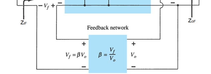
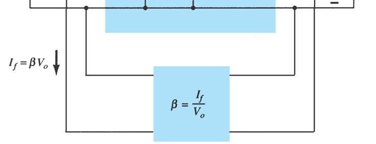
5 n Techncal Terms Summng Nde mplfer nput - Errr Feedback Netwrk Feedback s a technque t feed back a prtn f the utput sgnal (current r vltage) t the nput surce thrugh a feedback netwrk m f the crcut s t mnmse the errr 5
6 Type f Feedback Tw types f feedback Pstve (regeneratve) Negatve (degeneratve) The basc dea f negatve feedback s t trade ff gan fr ther desrable prpertes 6
7 Type f Feedback (cnt.) n negatve feedback systems, the feedback tends t reduce the nput t the frward path n pstve feedback systems, the feedback tends t ncrease the nput t the frward path Negatve feedback: Pstve feedback: β s pstve β s negatve and less than 1 ( pen-lp gan, β feedback netwrk) 7
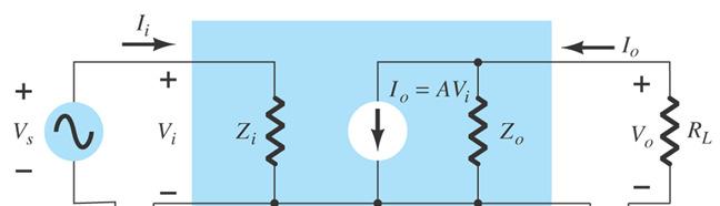
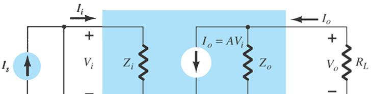
8 mplfer wthut Feedback X can be current r vltage sgnals s called an pen lp gan 8
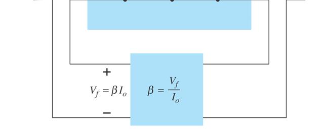
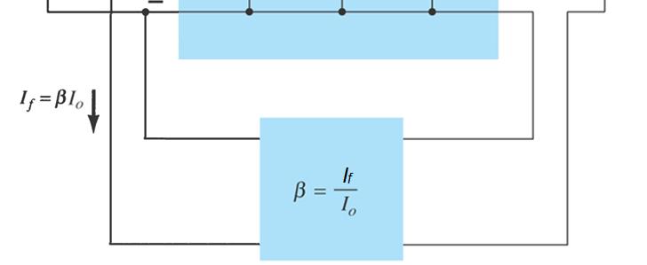
9 mplfer wth Feedback Fgure 3.2: X S X XO X f Feedback netwrk: Gan wthut feedback: Gan wth feedback: β F X X X X F X X s F s called an 9 clse lp gan
10 n Fg. 3.2: Gan wth Feedback X f β X X X S X f X S β X X X ( X S β X ) X ( 1 β) X S f X X s 1 β mplfer s gan wth feedback s reduced by the factr (1 β) Deselectvty D 1 β 10
11 Why Feedback? (dvantages) Desenstze the gan: make the value f the gan less senstve t varatns n the value f crcut cmpnents, such as mght be caused by changes n temperature better stablzed gan Overall gan wth negatve feedback: f 1 β f β >> 1 then: f β 1 β Gan wth feedback ( f ) s ndependent f amplfer gan (). f depends n feedback netwrk (β) 11
12 Why Feedback? (dvantages) Reduce nnlnear dstrtn: make the utput prprtnal t the nput mre lnear peratn Reduce the effect f nse: mnmze the cntrbutn t the utput f unwanted electrc sgnals generated, ether by the crcut cmpnents themselves, r by extraneus nterference reduced dstrtn f the utput sgnal Extend the bandwdth f the amplfer mprved frequency respnse 12
13 Frequency Respnse lthugh gan s reduced, BW s ncreased f Lf f L 1 β f Hf f 1 H 13 ( β )
14 Gan Bandwdth Prduct (GBP) GBP fr amplfer wth r wthut prduct s equal: ( BW ) ( BW ) f f Cutff frequences wth feedback: f Lf f L f f ( ) 1 Hf H 1 β β Bandwdth wth feedback: BW f f Hf f Lf snce f Hf >> f Lf then BW f f Hf BW f f f 1 Hf H ( β ) 14
15 Gan Bandwdth Prduct (GBP) GBP fr amplfer wth feedback: f x BW f β 1 β ( f H ( 1 ) ) f H Fr amplfer wthut feedback, the bandwdth: BW f H f L f The GBP fr amplfer wthut feedback: H Prven that: xbw f H ( BW ) ( BW ) f f 15
16 Why Feedback? (dvantages) Better nput and utput mpedances: rase r lwer the nput and utput mpedance by the selectn f an apprprate feedback tplgy accrdng t the type f amplfer hgher r lwer nput mpedance (Z ) hgher r lwer utput mpedance (Z ) Type f mplfer ltage mplfer Transmpedance mplfer Transcnductance mplfer Current mplfer Feedback Cnnectn ltage seres (shunt-seres) ltage shunt (shunt-shunt) Current seres (seres-seres) Current shunt (seres-shunt) 16
17 Feedback Cnnectn Types Bth vltage and current can be fed back t the nput ether n seres r parallel (shunt) 4 basc ways f cnnectng the feedback sgnal: ) vltage seres feedback (Fg.3.4(a)) ) vltage-shunt feedback (Fg.3.4(b)) ) current-seres feedback (Fg.3.4(c)) v) current-shunt feedback (Fg.3.4(d)) 17
 vltage-shunt feedback")
18 ltage mplfer (a) vltage-seres feedback (shunt-seres) ƒ / s Transmpedance/ transresstance mplfer (b) vltage-shunt feedback (shunt-shunt) ƒ / s 18

 current-shunt feedback")
19 Trancnductance mplfer (c) current-seres feedback (seres-seres) ƒ / s Current mplfer (d) current-shunt feedback (seres-shunt) ƒ / s 19
20 n Fg. 3.4, the terms vltage refers t cnnectng the utput vltage (Fg. a & b) as nput t the feedback netwrk whle current refers t tappng ff sme utput current (Fg. c & d) thrugh the feedback netwrk Seres refers t cnnectng the feedback sgnal n seres wth the nput sgnal vltage (Fg. a & c); whle shunt refers t cnnectng the feedback sgnal n shunt (parallel) wth an nput current surce (Fg. b & d) 20
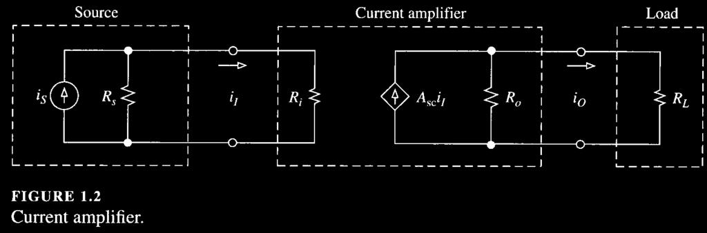
21 mplfer Fundamentals 21
22 mplfers Type f mplfer ltage mplfer Transmpedance mplfer Transcnductance mplfer Current mplfer Feedback Cnnectn ltage seres ltage shunt Current seres Current Shunt deal nput mpedance (Z) deal Output mpedance (Z) Gan wthut Feedback t tc 22
")
23 Fg. 3.5(a) ltage-seres Feedback 23


 s O s 1 β")
24 ltage-seres Feedback Fndng f Output f the crcut: O t the nput: s f and β f Hence: O ( ) ( β ) s f s f s f ( 1 β ) s O s 1 β 24
 s 1 Z")
25 ltage-seres Feedback ) f s (1 β β β Fndng Z 25 ) 1 ( v s F Z Z β Z nput mpedance s ncreased ( ) s 1 Z β
 Rewrtng the equatn v β Z Then the utput mpedance: Z f 1 Z v β")
26 Fndng Z ltage-seres Feedback Fr the crcut: Wth s 0 Z v - f Therefre Z v f Z v (β) Rewrtng the equatn v β Z Then the utput mpedance: Z f 1 Z v β 26
27 ltage-shunt Feedback Transmpedance mplfer 27
28 ltage-shunt Feedback ) (1 t t t t t s t f F β β β t 1 β F F s reduced 28 1 β t ) / ( / / f s F Z β β t F 1 Z Z β Z F s reduced


29 ltage-shunt Feedback Crcut n fndng utput mpedance 29

 t Z Z t ( β) Z F Z 1 β t Z F s")
30 ltage-shunt Feedback Z F can be fund n smlar manner as the vltage amplfer wth vltage seres feedback When s 0 - f Z t Therefre Z t f f β, s ( 1 β ) t Z Z t ( β) Z F Z 1 β t Z F s reduced 30
31 Current-Seres Feedback Transcnductance mplfer 31
32 Current-Seres Feedback tc F 1 β F s reduced tc β β β 1 tc f s Fndng gan wth feedback 32 tc f F β β β 1 tc tc tc tc tc s S tc 1 β nther way:
33 Current-Seres Feedback tc s s f s Z - Z - Z - Z β β tc s - Z β Fndng nput mpedance 33 ( ) tc s F 1 Z Z β Z F s ncreased tc s ( ) tc tc tc s 1 Z Z Z Z β β β


34 Current-Seres Feedback Crcut t fnd utput mpedance Wth s 0: - f 34
35 Current-Seres Feedback Fndng utput mpedance tc Z Wth s 0: - f and f β Z f tc (- f ) - tc β Z Z (1 β ) Z tc Z (1 βtc ) Z F s ncreased 35
36 Current-Shunt Feedback Current mplfer 36
37 Current-Shunt Feedback F β β 1 S F O F β 37 S F 1 β F s reduced F 1 β β β 1 s
38 Current-Shunt Feedback f s F Z Z Z / / β β F 1 Z Z β Z F s decreased 38 Z F s ncreased Z Z Z ) - (- f β ) (1 f Z Z β Z ) (1 β
39 Current-Shunt Feedback Crcut t fnd utput mpedance 39
40 Effect f Feedback n nput and Output mpedances Feedback Tplgy mplfer ltage ltage Current Current seres shunt seres shunt ltage Transmpe- Transcnduc- Current mplfer Transcnduc- Transmpedance mplfer tance mplfer mplfer Z F Z ( 1 β) 1Z β Z ( 1 β) 1Z β Z F Z β Z β 1 1 Z ( 1 β) Z ( 1 β) 40
41 mplfer & Feedback Tplgy 41
42 PRCTCL FEEDBCK CRCUTS 42
43 Feedback n Crcuts T determne the type f feedback emplyed by a crcut, a test can be dne t check ether the utput vltage ( ) r utput current ( ) s taken at the utput t be fed back Ths s dne usng test fr vltage r test fr current Then at the nput sectn, check the way the surce (X s ), nput (X ) and feedback (X f ) sgnals are cnnected: ether n seres r parallel (shunt) 43
44 Test fr ltage r Current Test fr vltage Shrt crcut the lad s that the utput vltage becmes zer f the sgnal returned t the amplfer nput by the feedback netwrk becmes zer, then the amplfer has a vltage feedback Test fr current Open crcut the lad s that the utput current becmes zer f the sgnal returned t the amplfer nput by the feedback netwrk als becmes zer, then the amplfer has a current feedback 44

, and gan fr ths")
45 Example 1 Determne the feedback tplgy used n the crcut Fnd the feedback netwrk (β), and gan fr ths crcut 45

46 Example 1 : Test fr ltage Shrt crcut the utput The utput vltage ( 0 ) s zer; and n utput sgnal s beng fed t the feedback netwrk Snce the sgnal returned t the amplfer nput by the feedback netwrk becmes zer, then the amplfer has a vltage feedback t the nput: Surce sgnal s n seres wth nput and feedback sgnals Thus t s a vltage seres feedback 46
47 Example 1 : Test fr Current Open crcut utput There s a current () beng fed t the feedback netwrk Snce the sgnal returned t the amplfer nput by the feedback netwrk s nt zer, then the utput sgnal beng taken s nt current, s the amplfer has a vltage feedback t the nput: Surce sgnal s n seres wth nput and feedback sgnals Thus t s a vltage seres feedback 47
48 Example 1 Fndng the feedback factr (β): F R R R R R R β F R R R S the feedback netwrk( β):
49 Example 1 Fndng the gan wth feedback s But - s F s F Thus: F O S O F 1 β R R F R 2 R1 R 2 49
50 Example 2 Determne the feedback tplgy used n the crcut Fnd the feedback netwrk (β), and gan fr ths crcut 50

51 Test fr vltage Shrt crcut the utput The utput vltage ( 0 ) s zer; but there s a sgnal beng fed t feedback netwrk Snce the sgnal returned t the amplfer nput by the feedback netwrk s nt zer, then t s nt the utput vltage beng taken t be fed back Example 2 Hence the amplfer has a current feedback 51
52 Test fr current Open crcut the utput There s n utput sgnal beng fed t feedback netwrk Snce the sgnal returned t the amplfer nput by the feedback netwrk s zer, then t s the utput current beng taken t be fed back Example 2 Hence the amplfer has a current feedback 52
53 Example 2 t the nput: Surce sgnal s n seres wth nput and feedback sgnals Thus t s a current seres feedback The amplfer s a transcnductance amplfer 53

54 Example 2 O F But 0 O F R F F F R F β O Feedback netwrk F - S F F F R F O R O S 1 R F tc mplfer s gan 54
55 Example 3 Determne the feedback tplgy used n the crcut 55
56 Test fr vltage Shrt crcut utput Output vltage wll be zer; n utput sgnal s beng fed t the feedback netwrk Snce the sgnal returned t the amplfer nput by the feedback netwrk becmes zer, then the amplfer has a vltage feedback Example 3 t the nput: Surce sgnal s parallel wth nput and feedback sgnals Thus t s a vltage shunt feedback 56
57 Test fr current Open crcut utput There s a current beng fed t the feedback netwrk Snce the sgnal returned t the amplfer nput by the feedback netwrk s nt zer, then the utput sgnal beng taken s nt current; t s the utput vltage Hence the amplfer has a vltage feedback Example 3 t the nput: Surce sgnal s parallel wth nput and feedback sgnals Thus t s a vltage shunt feedback 57
58 Example 3 Exercse: Fnd the feedback netwrk (β), and the gan fr ths crcut Ths crcut has a vltage shunt feedback Thus t s a transmpedance amplfer 58
59 Slutn fr Exercse (Example 3) F S 0 S F O O R 0 59 O O F R 1 β O S O F R O O R
60 POSTE FEEDBCK ND OSCLLTOR OPERTON 60
61 Oscllatr n scllatr s a crcut that prduces a perdc wavefrm n ts utput wth nly the dc supply vltage as an nput The utput vltage can be ether snusdal r nn- snusdal, dependng n the type f scllatr Fg. 3.9 dc supply vltage scllatr ut 61
62 Pstve Feedback Pstve feedback s used n a range f bth analgue and dgtal crcuts t prduce a varety f effects Pstve feedback Mst cmmnly used n the prductn f scllatrs Pstve feedback s characterzed by the cndtn wheren an n-phase prtn f the utput vltage f an amplfer s fed back t the nput wth n net phase shft 62
63 Pstve Feedback & Oscllatn ttal phase shft f 360 s ntrduced nvertng mplfer (θ 180 ) and f are n phase β O Fg Feedback netwrk (θ 180 ) 63
64 Pstve Feedback : nvertng mplfer Fg
65 Pstve Feedback : Nnnvertng mplfer n-phase f v Nnnvertng amplfer Feedback crcut 65
66 Oscllatn Frm the shwn fgure, the n-phase feedback vltage, f, s amplfed t prduce the utput vltage, whch n turn prduces the feedback vltage lp s created n whch the sgnal sustans tself and a cntnuus snusdal utput s prduced Ths phenmenn s called scllatn 66
67 Cndtns fr Oscllatn Tw cndtns are requred t sustan a state f scllatns: The phase shft arund the feedback lp must be effectvely 0 (r 360 ) The vltage gan, cl, arund the clsed feedback lp (lp gan) must equal t 1 (unty) These 2 cndtns are knwn as Barkhausen Crtern 67
68 Barkhausen Crtern f v f v Phase shft 0 cl v β 1 Feedback crcut Feedback crcut n-phase (a) (b) Fg : General cndtns t sustan scllatn : (a) The phase shft arund the lp s 0 (b) The clsed lp gan s 1 68
69 Start-up Cndtns t cc v cl v β t β cl > 1 cl 1 When scllatn starts at t, the cndtn cl > 1 causes the snusdal utput vltage ampltude t buld up t a desred level. Then cl decreases t 1 and mantans the desred ampltude. 69
70 Effects f v β n Oscllatr Operatn Fg. 3.12: (a) The utput s drven nt clppng when v β > 1 70
71 Effects f v β n scllatr peratn Fg. 3.12: (b) The utput fades ut when v β < 1 Dampng; The fadng and lss f scllatns that ccur when vβ < 1 71
72 Effects f v β n scllatr peratn Fg. 3.12: (c) cnstant-ampltude utput s prduced when v β 1 72
73 Q & 73
Feedback Principle :-
 Feedback Prncple : Feedback amplfer s that n whch a part f the utput f the basc amplfer s returned back t the nput termnal and mxed up wth the nternal nput sgnal. The sub netwrks f feedback amplfer are:
55:041 Electronic Circuits
 55:04 Electrnc Crcuts Feedback & Stablty Sectns f Chapter 2. Kruger Feedback & Stablty Cnfguratn f Feedback mplfer S S S S fb Negate feedback S S S fb S S S S S β s the feedback transfer functn Implct
Introduction to Electronic circuits.
 Intrductn t Electrnc crcuts. Passve and Actve crcut elements. Capactrs, esstrs and Inductrs n AC crcuts. Vltage and current dvders. Vltage and current surces. Amplfers, and ther transfer characterstc.
PHYSICS 536 Experiment 12: Applications of the Golden Rules for Negative Feedback
 PHYSICS 536 Experment : Applcatns f the Glden Rules fr Negatve Feedback The purpse f ths experment s t llustrate the glden rules f negatve feedback fr a varety f crcuts. These cncepts permt yu t create
Design of Analog Integrated Circuits
 Desgn f Analg Integrated Crcuts I. Amplfers Desgn f Analg Integrated Crcuts Fall 2012, Dr. Guxng Wang 1 Oerew Basc MOS amplfer structures Cmmn-Surce Amplfer Surce Fllwer Cmmn-Gate Amplfer Desgn f Analg
Circuits Op-Amp. Interaction of Circuit Elements. Quick Check How does closing the switch affect V o and I o?
 Crcuts Op-Amp ENGG1015 1 st Semester, 01 Interactn f Crcut Elements Crcut desgn s cmplcated by nteractns amng the elements. Addng an element changes vltages & currents thrughut crcut. Example: clsng a
III. Operational Amplifiers
 III. Operatnal Amplfers Amplfers are tw-prt netwrks n whch the utput vltage r current s drectly prprtnal t ether nput vltage r current. Fur dfferent knds f amplfers ext: ltage amplfer: Current amplfer:
Chapter 7. Systems 7.1 INTRODUCTION 7.2 MATHEMATICAL MODELING OF LIQUID LEVEL SYSTEMS. Steady State Flow. A. Bazoune
 Chapter 7 Flud Systems and Thermal Systems 7.1 INTODUCTION A. Bazune A flud system uses ne r mre fluds t acheve ts purpse. Dampers and shck absrbers are eamples f flud systems because they depend n the
ME2142/ME2142E Feedback Control Systems. Modelling of Physical Systems The Transfer Function
 Mdellng Physcal Systems The Transer Functn Derental Equatns U Plant Y In the plant shwn, the nput u aects the respnse the utput y. In general, the dynamcs ths respnse can be descrbed by a derental equatn
EE 204 Lecture 25 More Examples on Power Factor and the Reactive Power
 EE 204 Lecture 25 Mre Examples n Pwer Factr and the Reactve Pwer The pwer factr has been defned n the prevus lecture wth an example n pwer factr calculatn. We present tw mre examples n ths lecture. Example
Lecture 2 Feedback Amplifier
 Lectue Feedback mple ntductn w-pt Netwk Negatve Feedback Un-lateal Case Feedback plg nalss eedback applcatns Clse-Lp Gan nput/output esstances e:83hkn 3 Feedback mples w-pt Netwk z-paametes Open-Ccut mpedance
PT326 PROCESS TRAINER
 PT326 PROCESS TRAINER 1. Descrptn f the Apparatus PT 326 Prcess Traner The PT 326 Prcess Traner mdels cmmn ndustral stuatns n whch temperature cntrl s requred n the presence f transprt delays and transfer
Linear Amplifiers and OpAmps
 Lnear Amplfers and OpAmps eferences: Barbw (pp 7-80), Hayes & Hrwtz (pp 63-40), zzn (Chapter ) Amplfers are tw-prt netwrks n whch the utput ltage r current s drectly prprtnal t ether nput ltage r current.
Chapter 3, Solution 1C.
 COSMOS: Cmplete Onlne Slutns Manual Organzatn System Chapter 3, Slutn C. (a If the lateral surfaces f the rd are nsulated, the heat transfer surface area f the cylndrcal rd s the bttm r the tp surface
The three major operations done on biological signals using Op-Amp:
 The three majr peratns dne n blgcal sgnals usng Op-Amp: ) Amplcatns and Attenuatns 2) DC settng: add r subtract a DC 3) Shape ts requency cntent: Flterng Ideal Op-Amp Mst belectrc sgnals are small and
CHAPTER 3 ANALYSIS OF KY BOOST CONVERTER
 70 CHAPTER 3 ANALYSIS OF KY BOOST CONERTER 3.1 Intrductn The KY Bst Cnverter s a recent nventn made by K.I.Hwu et. al., (2007), (2009a), (2009b), (2009c), (2010) n the nn-slated DC DC cnverter segment,
Introduction of Two Port Network Negative Feedback (Uni lateral Case) Feedback Topology Analysis of feedback applications
 Feedback Topology Analysis of feedback applications") Lectue Feedback mple ntductn w Pt Netwk Negatve Feedback Un lateal Case Feedback plg nalss eedback applcatns Clse Lp Gan nput/output esstances e:83h 3 Feedback w-pt Netwk z-paametes Open-Ccut mpedance
Lectue Feedback mple ntductn w Pt Netwk Negatve Feedback Un lateal Case Feedback plg nalss eedback applcatns Clse Lp Gan nput/output esstances e:83h 3 Feedback w-pt Netwk z-paametes Open-Ccut mpedance
SIMULATION OF THREE PHASE THREE LEG TRANSFORMER BEHAVIOR UNDER DIFFERENT VOLTAGE SAG TYPES
 SIMULATION OF THREE PHASE THREE LEG TRANSFORMER BEHAVIOR UNDER DIFFERENT VOLTAGE SAG TYPES Mhammadreza Dlatan Alreza Jallan Department f Electrcal Engneerng, Iran Unversty f scence & Technlgy (IUST) e-mal:
ANALOG ELECTRONICS 1 DR NORLAILI MOHD NOH
 24 ANALOG LTRONIS TUTORIAL DR NORLAILI MOHD NOH . 0 8kΩ Gen, Y β β 00 T F 26, 00 0.7 (a)deterne the dc ltages at the 3 X ternals f the JT (,, ). 0kΩ Z (b) Deterne g,r π and r? (c) Deterne the ltage gan
EE 221 Practice Problems for the Final Exam
 EE 1 Practce Prblems fr the Fnal Exam 1. The netwrk functn f a crcut s 1.5 H. ω 1+ j 500 Ths table recrds frequency respnse data fr ths crcut. Fll n the blanks n the table:. The netwrk functn f a crcut
The Operational Amplifier and Application
 Intrductn t Electrnc Crcuts: A Desgn Apprach Jse Sla-Martnez and Marn Onabaj The Operatnal Amplfer and Applcatn The peratnal ltage amplfer (mre cmmnly referred t as peratnal amplfer) s ne f the mst useful
CIRCUIT ANALYSIS II Chapter 1 Sinusoidal Alternating Waveforms and Phasor Concept. Sinusoidal Alternating Waveforms and
 U ANAYSS hapter Snusdal Alternatng Wavefrs and Phasr ncept Snusdal Alternatng Wavefrs and Phasr ncept ONNS. Snusdal Alternatng Wavefrs.. General Frat fr the Snusdal ltage & urrent.. Average alue..3 ffectve
IGEE 401 Power Electronic Systems. Solution to Midterm Examination Fall 2004
 Jós, G GEE 401 wer Electrnc Systems Slutn t Mdterm Examnatn Fall 2004 Specal nstructns: - Duratn: 75 mnutes. - Materal allwed: a crb sheet (duble sded 8.5 x 11), calculatr. - Attempt all questns. Make
Wp/Lmin. Wn/Lmin 2.5V
 UNIVERITY OF CALIFORNIA Cllege f Engneerng Department f Electrcal Engneerng and Cmputer cences Andre Vladmrescu Hmewrk #7 EEC Due Frday, Aprl 8 th, pm @ 0 Cry Prblem #.5V Wp/Lmn 0.0V Wp/Lmn n ut Wn/Lmn.5V
Section I5: Feedback in Operational Amplifiers
 Sectin I5: eedback in Operatinal mplifiers s discussed earlier, practical p-amps hae a high gain under dc (zer frequency) cnditins and the gain decreases as frequency increases. This frequency dependence
Waveshapping Circuits and Data Converters. Lesson #17 Comparators and Schmitt Triggers Section BME 373 Electronics II J.
 Waeshappg Crcuts and Data Cnerters Lessn #7 Cmparatrs and Schmtt Trggers Sectn. BME 7 Electrncs II 0 Waeshappg Crcuts and Data Cnerters Cmparatrs and Schmtt Trggers Astable Multbratrs and Tmers ectfers,
FE REVIEW OPERATIONAL AMPLIFIERS (OP-AMPS)( ) 8/25/2010
( ) 8/25/2010") FE REVEW OPERATONAL AMPLFERS (OP-AMPS)( ) 1 The Op-amp 2 An op-amp has two nputs and one output. Note the op-amp below. The termnal labeled l wth the (-) sgn s the nvertng nput and the nput labeled wth
FE REVEW OPERATONAL AMPLFERS (OP-AMPS)( ) 1 The Op-amp 2 An op-amp has two nputs and one output. Note the op-amp below. The termnal labeled l wth the (-) sgn s the nvertng nput and the nput labeled wth
Novel current mode AC/AC converters with high frequency ac link *
 vel current mde AC/AC cnverters wth hgh frequency ac lnk * Dalan Chen, e, Jan u, Shengyang n, Chen Sng Department f Electrcal Engneerng, anjng nversty f Aernautcs & Astrnautcs, anjng, Jangsu, 006 P.R.Chna
The two main types of FETs are the junction field effect transistor (JFET) and the metal oxide field effect transistor (MOSFET).
 and the metal oxide field effect transistor (MOSFET).") Mcrelectrncs Chapter three: Feld Effect Transstr sall snal analyss Intrductn: Feld-effect transstr aplfers prde an excellent ltae an wth the added feature f hh nput pedance. They are als lw-pwercnsuptn
Mcrelectrncs Chapter three: Feld Effect Transstr sall snal analyss Intrductn: Feld-effect transstr aplfers prde an excellent ltae an wth the added feature f hh nput pedance. They are als lw-pwercnsuptn
Faculty of Engineering
 Faculty f Engneerng DEPARTMENT f ELECTRICAL AND ELECTRONIC ENGINEERING EEE 223 Crcut Thery I Instructrs: M. K. Uygurğlu E. Erdl Fnal EXAMINATION June 20, 2003 Duratn : 120 mnutes Number f Prblems: 6 Gd
Conduction Heat Transfer
 Cnductn Heat Transfer Practce prblems A steel ppe f cnductvty 5 W/m-K has nsde and utsde surface temperature f C and 6 C respectvely Fnd the heat flw rate per unt ppe length and flux per unt nsde and per
FYSE400 ANALOG ELECTRONICS
 YS400 NLOG LCONCS LCU 12 eedback plfer 1 uptn 1. he bac aplfer unlateral. 2. he gan OL f the bac aplfer deterned wthut feedback. 3. he calculated gan OL laded gan : ladng f the feedback netwrk, urce and
55:141 Advanced Circuit Techniques Two-Port Theory
 55:4 Adanced Crcut Technques Two-Port Theory Materal: Lecture Notes A. Kruger 55:4: Adanced Crcut Technques The Unersty of Iowa, 03 Two-Port Theory, Slde What Are Two-Ports? Basc dea: replace a complex
CTN 2/23/16. EE 247B/ME 218: Introduction to MEMS Design Lecture 11m2: Mechanics of Materials. Copyright 2016 Regents of the University of California
 Vlume Change fr a Unaxal Stress Istrpc lastcty n 3D Istrpc = same n all drectns The cmplete stress-stran relatns fr an strpc elastc Stresses actng n a dfferental vlume element sld n 3D: (.e., a generalzed
Big Data Analytics! Special Topics for Computer Science CSE CSE Mar 31
 Bg Data Analytcs! Specal Tpcs fr Cmputer Scence CSE 4095-001 CSE 5095-005! Mar 31 Fe Wang Asscate Prfessr Department f Cmputer Scence and Engneerng fe_wang@ucnn.edu Intrductn t Deep Learnng Perceptrn In
Department of Electrical and Computer Engineering FEEDBACK AMPLIFIERS
 Department o Electrcal and Computer Engneerng UNIT I EII FEEDBCK MPLIFIES porton the output sgnal s ed back to the nput o the ampler s called Feedback mpler. Feedback Concept: block dagram o an ampler
Part III Lectures Field-Effect Transistors (FETs) and Circuits
 and Circuits") Part III Lecture 5-8 Feld-Effect Trantr (FET) and Crcut Unverty f Technlgy Feld-Effect Trantr (FET) Electrcal and Electrnc Engneerng epartment Lecture Ffteen - Page f 8 ecnd Year, Electrnc I, 2009-200
Part III Lecture 5-8 Feld-Effect Trantr (FET) and Crcut Unverty f Technlgy Feld-Effect Trantr (FET) Electrcal and Electrnc Engneerng epartment Lecture Ffteen - Page f 8 ecnd Year, Electrnc I, 2009-200
Copyright Paul Tobin 63
 DT, Kevin t. lectric Circuit Thery DT87/ Tw-Prt netwrk parameters ummary We have seen previusly that a tw-prt netwrk has a pair f input terminals and a pair f utput terminals figure. These circuits were
Section 3: Detailed Solutions of Word Problems Unit 1: Solving Word Problems by Modeling with Formulas
 Sectn : Detaled Slutns f Wrd Prblems Unt : Slvng Wrd Prblems by Mdelng wth Frmulas Example : The factry nvce fr a mnvan shws that the dealer pad $,5 fr the vehcle. If the stcker prce f the van s $5,, hw
OP AMP CHARACTERISTICS
 O AM CHAACTESTCS Static p amp limitatins EFEENCE: Chapter 5 textbk (ESS) EOS CAUSED BY THE NUT BAS CUENT AND THE NUT OFFSET CUENT Op Amp t functin shuld have fr the input terminals a DC path thrugh which
Is current gain generally significant in FET amplifiers? Why or why not? Substitute each capacitor with a
 FET Sall Snal Mdband Mdel Ntatn: C arables and quanttes are enerally desnated wth an uppercase subscrpt. AC arables and quanttes are enerally desnated wth a lwercase subscrpt. Phasr ntatn wll be used when
Module B3. VLoad = = V S V LN
 Mdule B Prblem The -hase lads are cnnected n arallel. One s a urely resste lad cnnected n wye. t cnsumes 00kW. The secnd s a urely nducte 00kR lad cnnected n wye. The thrd s a urely caacte 00kR lad cnnected
55:141 Advanced Circuit Techniques Two-Port Theory
 55:4 Adanced Crcut Technques Two-Port Theory Materal: Lecture Notes A. Kruger 55:4: Adanced Crcut Technques The Unersty of Iowa, 205 Two-Port Theory, Slde Two-Port Networks Note, the BJT s all are hghly
55:041 Electronic Circuits
 55:04 Electronc Crcuts Feedback & Stablty Sectons of Chapter 2. Kruger Feedback & Stablty Confguraton of Feedback mplfer Negate feedback β s the feedback transfer functon S o S S o o S S o f S S S S fb
55:041 Electronic Circuits
 55:04 Electronc Crcuts Feedback & Stablty Sectons of Chapter 2. Kruger Feedback & Stablty Confguraton of Feedback mplfer S o S ε S o ( S β S ) o Negate feedback S S o + β β s the feedback transfer functon
V. Electrostatics Lecture 27a: Diffuse charge at electrodes
 V. Electrstatcs Lecture 27a: Dffuse charge at electrdes Ntes by MIT tudent We have talked abut the electrc duble structures and crrespndng mdels descrbng the n and ptental dstrbutn n the duble layer. Nw
Energy & Work
 rk Dne by a Cntant Frce 6.-6.4 Energy & rk F N m jule () J rk Dne by a Cntant Frce Example Pullng a Sutcae-n-heel Fnd the wrk dne the rce 45.0-N, the angle 50.0 degree, and the dplacement 75.0 m. 3 ( F
T-model: - + v o. v i. i o. v e. R i
 T-mdel: e gm - V Rc e e e gme R R R 23 e e e gme R R The s/c tanscnductance: G m e m g gm e 0 The nput esstance: R e e e e The utput esstance: R R 0 /c unladed ltage gan, R a g R m e gmr e 0 m e g me e/e
FEEDBACK AMPLIFIERS. v i or v s v 0
 FEEDBCK MPLIFIERS Feedback n mplers FEEDBCK IS THE PROCESS OF FEEDING FRCTION OF OUTPUT ENERGY (VOLTGE OR CURRENT) BCK TO THE INPUT CIRCUIT. THE CIRCUIT EMPLOYED FOR THIS PURPOSE IS CLLED FEEDBCK NETWORK.
Edexcel GCSE Physics
 Edexcel GCSE Physics Tpic 10: Electricity and circuits Ntes (Cntent in bld is fr Higher Tier nly) www.pmt.educatin The Structure f the Atm Psitively charged nucleus surrunded by negatively charged electrns
Lesson 5. Thermomechanical Measurements for Energy Systems (MENR) Measurements for Mechanical Systems and Production (MMER)
 Measurements for Mechanical Systems and Production (MMER)") Lessn 5 Thermmechancal Measurements r Energy Systems (MEN) Measurements r Mechancal Systems and Prductn (MME) A.Y. 205-6 Zaccara (n ) Del Prete We wll nw analyze mre n depth each ne the unctnal blcks the
Lessn 5 Thermmechancal Measurements r Energy Systems (MEN) Measurements r Mechancal Systems and Prductn (MME) A.Y. 205-6 Zaccara (n ) Del Prete We wll nw analyze mre n depth each ne the unctnal blcks the
Thermodynamics of Materials
 Thermdynamcs f Materals 14th Lecture 007. 4. 8 (Mnday) FUGACITY dg = Vd SdT dg = Vd at cnstant T Fr an deal gas dg = (RT/)d = RT dln Ths s true fr deal gases nly, but t wuld be nce t have a smlar frm fr
FE REVIEW OPERATIONAL AMPLIFIERS (OP-AMPS)
") FE EIEW OPEATIONAL AMPLIFIES (OPAMPS) 1 The Opamp An opamp has two nputs and one output. Note the opamp below. The termnal labeled wth the () sgn s the nvertng nput and the nput labeled wth the () sgn
FE EIEW OPEATIONAL AMPLIFIES (OPAMPS) 1 The Opamp An opamp has two nputs and one output. Note the opamp below. The termnal labeled wth the () sgn s the nvertng nput and the nput labeled wth the () sgn
A Novel Isolated Buck-Boost Converter
 vel slated uck-st Cnverter S-Sek Kim *,WOO-J JG,JOOG-HO SOG, Ok-K Kang, and Hee-Jn Kim ept. f Electrical Eng., Seul atinal University f Technlgy, Krea Schl f Electrical and Cmputer Eng., Hanyang University,
_J _J J J J J J J J _. 7 particles in the blue state; 3 particles in the red state: 720 configurations _J J J _J J J J J J J J _
 Dsrder and Suppse I have 10 partcles that can be n ne f tw states ether the blue state r the red state. Hw many dfferent ways can we arrange thse partcles amng the states? All partcles n the blue state:
Technote 6. Op Amp Definitions. April 1990 Revised 11/22/02. Tim J. Sobering SDE Consulting
 Technte 6 prl 990 Resed /22/02 Op mp Dentns Tm J. Sberng SDE Cnsultng sdecnsultng@pbx.cm 990 Tm J. Sberng. ll rghts resered. Op mp Dentns Pge 2 Op mp Dentns Ths Technte summrzes the bsc pertnl mpler dentns
Two Port Characterizations
 lectronc Crcuts Two Port Characterzatons Contents Input and output resstances Two port networks Models Prof. C.K. Tse: -port networks Impedances and loadng effects Voltage amplfers R s R out smaller the
ANALOG ELECTRONICS DR NORLAILI MOHD NOH
 24 ANALOG LTRONIS lass 5&6&7&8&9 DR NORLAILI MOHD NOH 3.3.3 n-ase cnfguatn V V Rc I π π g g R V /p sgnal appled t. O/p taken f. ted t ac gnd. The hybd-π del pdes an accuate epesentatn f the sall-sgnal
Chapter 6 : Gibbs Free Energy
 Wnter 01 Chem 54: ntrductry hermdynamcs Chapter 6 : Gbbs Free Energy... 64 Defntn f G, A... 64 Mawell Relatns... 65 Gbbs Free Energy G(,) (ure substances)... 67 Gbbs Free Energy fr Mtures... 68 ΔG f deal
CIRCLE YOUR DIVISION: Div. 1 (9:30 am) Div. 2 (11:30 am) Div. 3 (2:30 pm) Prof. Ruan Prof. Naik Mr. Singh
 Div. 2 (11:30 am) Div. 3 (2:30 pm) Prof. Ruan Prof. Naik Mr. Singh") Frst CIRCLE YOUR DIVISION: Dv. 1 (9:30 am) Dv. (11:30 am) Dv. 3 (:30 m) Prf. Ruan Prf. Na Mr. Sngh Schl f Mechancal Engneerng Purdue Unversty ME315 Heat and Mass ransfer Eam #3 Wednesday Nvember 17 010
Frst CIRCLE YOUR DIVISION: Dv. 1 (9:30 am) Dv. (11:30 am) Dv. 3 (:30 m) Prf. Ruan Prf. Na Mr. Sngh Schl f Mechancal Engneerng Purdue Unversty ME315 Heat and Mass ransfer Eam #3 Wednesday Nvember 17 010
CHAPTER 11. Solutions for Exercises. (b) An inverting amplifier has negative gain. Thus L
 An inverting amplifier has negative gain. Thus L") CHPTE Slutn fr Exerce E. (a nnnertng amplfer ha pte gan. Thu ( t ( t 50 ( t 5.0 n(000πt (b n nertng amplfer ha negate gan. Thu ( t ( t 50 ( t 5.0 n(000πt E. V V 75 500 + 5+ 75 c 75 V 000 75 500 V + + 500
CHPTE Slutn fr Exerce E. (a nnnertng amplfer ha pte gan. Thu ( t ( t 50 ( t 5.0 n(000πt (b n nertng amplfer ha negate gan. Thu ( t ( t 50 ( t 5.0 n(000πt E. V V 75 500 + 5+ 75 c 75 V 000 75 500 V + + 500
Diodes Waveform shaping Circuits. Sedra & Smith (6 th Ed): Sec. 4.5 & 4.6 Sedra & Smith (5 th Ed): Sec. 3.5 & 3.6
: Sec. 4.5 & 4.6 Sedra & Smith (5 th Ed): Sec. 3.5 & 3.6") des Waefrm shapng Cruts Sedra & Smth (6 th Ed): Se. 4.5 & 4.6 Sedra & Smth (5 th Ed): Se. 3.5 & 3.6 Tw-prt netwrks as buldng blks Reall: Transfer funtn f a tw-prt netwrk an be fund by slng ths rut ne.
des Waefrm shapng Cruts Sedra & Smth (6 th Ed): Se. 4.5 & 4.6 Sedra & Smth (5 th Ed): Se. 3.5 & 3.6 Tw-prt netwrks as buldng blks Reall: Transfer funtn f a tw-prt netwrk an be fund by slng ths rut ne.
Chapter II Circuit Analysis Fundamentals
 Chapter II Crcut nalyss Fundamentals Frm a desgn engneer s perspecte, t s mre releant t understand a crcut s peratn and lmtatns than t fnd eact mathematcal epressns r eact numercal slutns. Precse results
Concurrent Adaptive Cancellation of Quantization Noise and Harmonic Distortion in Sigma Delta Converter
 Internatnal Jurnal f Cmputer Engneerng Scence (IJCES) Vlume 2 Issue 11 (vember 2012) ISS : 2250:3439 https://stes.ggle.cm/ste/jcesjurnal http://www.jces.cm/ Cncurrent Adaptve Cancellatn f Quantzatn se
EE C245 ME C218 Introduction to MEMS Design
 EE C45 ME C8 Introducton to MEM Desgn Fall 7 Prof. Clark T.C. Nguyen Dept. of Electrcal Engneerng & Computer cences Unersty of Calforna at Berkeley Berkeley, C 947 Dscusson: eew of Op mps EE C45: Introducton
Revision: August 19, E Main Suite D Pullman, WA (509) Voice and Fax
 Voice and Fax") .7.4: Direct frequency dmain circuit analysis Revisin: August 9, 00 5 E Main Suite D Pullman, WA 9963 (509) 334 6306 ice and Fax Overview n chapter.7., we determined the steadystate respnse f electrical
.7.4: Direct frequency dmain circuit analysis Revisin: August 9, 00 5 E Main Suite D Pullman, WA 9963 (509) 334 6306 ice and Fax Overview n chapter.7., we determined the steadystate respnse f electrical
Physic 231 Lecture 33
 Physc 231 Lecture 33 Man pnts f tday s lecture: eat and heat capacty: Q cm Phase transtns and latent heat: Q Lm ( ) eat flw Q k 2 1 t L Examples f heat cnductvty, R values fr nsulatrs Cnvectn R L / k Radatn
Diodes Waveform shaping Circuits
 des Waefrm shapng Cruts Leture ntes: page 2-2 t 2-31 Sedra & Smth (6 th Ed): Se. 4.5 & 4.6 Sedra & Smth (5 th Ed): Se. 3.5 & 3.6 F. Najmabad, ECE65, Wnter 212 Tw-prt netwrks as buldng blks Reall: Transfer
Microelectronics Circuit Analysis and Design. NMOS Common-Source Circuit. NMOS Common-Source Circuit 10/15/2013. In this chapter, we will:
 Mcrelectrncs Crcut Analyss and Desn Dnald A. Neaen Chapter 4 Basc FET Aplfers In ths chapter, we wll: Inestate a snle-transstr crcut that can aplfy a sall, te-aryn nput snal Deelp sall-snal dels that are
Lesson #14. Section BME 373 Electronics II J.Schesser
 Feedback and Oscillatrs Lessn #4 Impedances Sectin 9.35 65 Types f ffeedback Type f ffeedback k(the utput tentity fed dback): Vltage Feedback s. Current Feedback β s. β Hw it is achieed (the means t fed
element k Using FEM to Solve Truss Problems
 sng EM t Slve Truss Prblems A truss s an engneerng structure cmpsed straght members, a certan materal, that are tpcall pn-ned at ther ends. Such members are als called tw-rce members snce the can nl transmt
CHAPTER 3 QUASI-RESONANT BUCK CONVERTER
 27 CHAPTER 3 QUASI-RESONANT BUCK CONVERTER Hstrcally, prr t the avalablty f cntrllable swtch wth apprecable vltage and current-handlng capablty, the swtch-mde DC-DC cnverter cnssts f thyrstrs whch pertans
Week 11: Differential Amplifiers
 ELE 0A Electronc rcuts Week : Dfferental Amplfers Lecture - Large sgnal analyss Topcs to coer A analyss Half-crcut analyss eadng Assgnment: hap 5.-5.8 of Jaeger and Blalock or hap 7. - 7.3, of Sedra and
Improved Bridgeless Interleaved Boost PFC Rectifier with Optimized Magnetic Utilization and Reduced Sensing Noise
 Jurnal f Pwer Electrncs, Vl. 14, N. 5, pp. 815-86, September 014 815 JPE 14-5-1 http://dx.d.rg/10.6113/jpe.014.14.5.815 ISSN(Prnt): 1598-09 / ISSN(Onlne): 093-4718 Imprved Brdgeless Interleaved Bst PFC
6. ELUTRIATION OF PARTICLES FROM FLUIDIZED BEDS
 6. ELUTRIATION OF PARTICLES FROM FLUIDIZED BEDS Elutratn s the prcess n whch fne partcles are carred ut f a fludzed bed due t the flud flw rate passng thrugh the bed. Typcally, fne partcles are elutrated
Lecture 20a. Circuit Topologies and Techniques: Opamps
 Lecture a Circuit Tplgies and Techniques: Opamps In this lecture yu will learn: Sme circuit tplgies and techniques Intrductin t peratinal amplifiers Differential mplifier IBIS1 I BIS M VI1 vi1 Vi vi I
BME 5742 Biosystems Modeling and Control
 BME 5742 Bsystems Mdeln and Cntrl Cell Electrcal Actvty: In Mvement acrss Cell Membrane and Membrane Ptental Dr. Zv Rth (FAU) 1 References Hppensteadt-Peskn, Ch. 3 Dr. Rbert Farley s lecture ntes Inc Equlbra
Bipolar-Junction (BJT) transistors
 transistors") Bplar-Junctn (BJT) transstrs References: Hayes & Hrwtz (pp 84-4), Rzzn (chapters 8 & 9) A bplar junctn transstr s frmed by jnng three sectns f semcnductrs wth alternately dfferent dpngs. The mddle sectn
Bplar-Junctn (BJT) transstrs References: Hayes & Hrwtz (pp 84-4), Rzzn (chapters 8 & 9) A bplar junctn transstr s frmed by jnng three sectns f semcnductrs wth alternately dfferent dpngs. The mddle sectn
Chapter 30. Inductance
 Chapter 30 nductance 30. Self-nductance Cnsider a lp f wire at rest. f we establish a current arund the lp, it will prduce a magnetic field. Sme f the magnetic field lines pass thrugh the lp. et! be the
Voltage Mode-to-Current Mode Transformation
 Tejmal S Rathre et al / nternatnal Jurnal f Engneerng and Technlgy (JET) ltage Mde-t-Current Mde Transfrmatn Tejmal S Rathre 1 and Uday P Kht Electrncs and Telecmmuncatn Engneerng Department, St Francs
Spring 2002 Lecture #17
 1443-51 Sprng 22 Lecture #17 r. Jaehn Yu 1. Cndtns fr Equlbrum 2. Center f Gravty 3. Elastc Prpertes f Slds Yung s dulus Shear dulus ulk dulus Tday s Hmewrk Assgnment s the Hmewrk #8!!! 2 nd term eam n
Coupled Inductors and Transformers
 Cupled nductrs and Transfrmers Self-nductance When current i flws thrugh the cil, a magnetic flux is prduced arund it. d d di di v= = = dt di dt dt nductance: = d di This inductance is cmmnly called self-inductance,
Lecture 02 CSE 40547/60547 Computing at the Nanoscale
 PN Junctin Ntes: Lecture 02 CSE 40547/60547 Cmputing at the Nanscale Letʼs start with a (very) shrt review f semi-cnducting materials: - N-type material: Obtained by adding impurity with 5 valence elements
Transfer Characteristic
 Eeld-Effect Transstors (FETs 3.3 The CMS Common-Source Amplfer Transfer Characterstc Electronc Crcuts, Dept. of Elec. Eng., The Chnese Unersty of Hong Kong, Prof. K.-L. Wu Lesson 8&9 Eeld-Effect Transstors
Simple electronically tunable oscillators
 Smple electrncally tunable scllatrs Mlan Strk, Petr Wessar, and Kaml Ksturk,, epartment Appled Electrncs and Telecmmuncatns/RIE, Faculty Electrcal Engneerng, Umversty West Bhema, zech Republc strk@kae.zcu.cz,
Synchronous Motor V-Curves
 Synchrnus Mtr V-Curves 1 Synchrnus Mtr V-Curves Intrductin Synchrnus mtrs are used in applicatins such as textile mills where cnstant speed peratin is critical. Mst small synchrnus mtrs cntain squirrel
POWER AMPLIFIERS. 1. Explain what are classes A, B, AB and C amplifiers in terms of DC biasing using a MOSFET drain characteristic.
 CTONIC 3 XCI OW AMII. xpla what are classes A, B, AB and C amplifiers terms f DC biasg usg a MOT dra characteristic.. efer t the graphs f page and the table at the tp f page 3 f the thery ntes t answer
Improved Bridgeless Interleaved Boost PFC Rectifier with Optimized Magnetic Utilization and Reduced Sensing Noise
 Jurnal f Pwer Electrncs, Vl. 14, N. 5, pp.???-???, September 014 1 JPE 14-5- http://dx.d.rg/10.6113/jpe.014.14.5.??? ISSN(Prnt): 1598-09 / ISSN(Onlne): 093-4718 Imprved Brdgeless Interleaved Bst PFC Rectfer
Chapter 10 Diodes. 1. Understand diode operation and select diodes for various applications.
 Chapter 10 des 1. Understand dde peratn and select ddes fr arus applcatns. 2. nalyze nnlnear crcuts usng the graphcal lad-lne technque. 3. nalyze and desgn smple ltage-regulatr crcuts. 4. Sle crcuts usng
Exercises for Frequency Response. ECE 102, Winter 2011, F. Najmabadi
 Eercses r Frequency espnse EE 0, Wnter 0, F. Najabad Eercse : A Mdy the crcut belw t nclude a dnant ple at 00 Mz ( 00 Ω, k, k, / 00 Ω, λ 0, and nre nternal capactances the MOS. pute the dnant ple n the
Water vapour balance in a building moisture exposure for timber structures
 Jnt Wrkshp f COST Actns TU1 and E55 September 21-22 9, Ljubljana, Slvena Water vapur balance n a buldng msture expsure fr tmber structures Gerhard Fnk ETH Zurch, Swtzerland Jchen Köhler ETH Zurch, Swtzerland
Oscillator. Introduction of Oscillator Linear Oscillator. Stability. Wien Bridge Oscillator RC Phase-Shift Oscillator LC Oscillator
 Oscillatr Intrductin f Oscillatr Linear Oscillatr Wien Bridge Oscillatr Phase-Shift Oscillatr L Oscillatr Stability Oscillatrs Oscillatin: an effect that repeatedly and regularly fluctuates abut the mean
Shell Stiffness for Diffe ent Modes
 Engneerng Mem N 28 February 0 979 SUGGESTONS FOR THE DEFORMABLE SUBREFLECTOR Sebastan vn Herner Observatns wth the present expermental versn (Engneerng Dv nternal Reprt 09 July 978) have shwn that a defrmable
Transistors. Lesson #10 Chapter 4. BME 372 Electronics I J.Schesser
 Tanssts essn #10 Chapte 4 BM 372 lectncs 154 Hmewk Ps. 4.40, 4.42, 4.43, 4.45, 4.46, 4.51, 4.53, 4.54, 4.56 BM 372 lectncs 155 Hmewk Answes #20 Ps. 4.40 See fgue 4.33 BM 372 lectncs 156 Ps. 4.42 Hmewk
General Amplifiers. Analog Electronics Circuits Nagamani A N. Lecturer, PESIT, Bangalore 85. Cascade connection - FET & BJT
 Analg lectrnics Circuits Nagamani A N Lecturer, PST, Bangalre 85 mail nagamani@pes.edu General Amplifiers Cascade cnnectin - FT & BJT Numerical Cascde cnnectin arlingtn cnnectin Packaged arlingtn cnnectin
ZVS Boost Converter. (a) (b) Fig 6.29 (a) Quasi-resonant boost converter with M-type switch. (b) Equivalent circuit.
 (b) Fig 6.29 (a) Quasi-resonant boost converter with M-type switch. (b) Equivalent circuit.") EEL6246 Pwer Electrnics II Chapter 6 Lecture 6 Dr. Sam Abdel-Rahman ZVS Bst Cnverter The quasi-resnant bst cnverter by using the M-type switch as shwn in Fig. 6.29(a) with its simplified circuit shwn in
EEL6246 Pwer Electrnics II Chapter 6 Lecture 6 Dr. Sam Abdel-Rahman ZVS Bst Cnverter The quasi-resnant bst cnverter by using the M-type switch as shwn in Fig. 6.29(a) with its simplified circuit shwn in
CHEM Thermodynamics. Change in Gibbs Free Energy, G. Review. Gibbs Free Energy, G. Review
 Review Accrding t the nd law f Thermdynamics, a prcess is spntaneus if S universe = S system + S surrundings > 0 Even thugh S system
MODULE TITLE : ELECTRONICS TOPIC TITLE : AMPLIFIERS LESSON 1 : FEEDBACK
 MODULE TITLE : ELECTONICS TOPIC TITLE : AMPLIFIES LESSON : FEEDBACK EL - 3 - INTODUCTION This lessn trduces the ideas f negative feedback, which we shw can vercme the disadvantages f wide parameter variat
Lecture 12. Heat Exchangers. Heat Exchangers Chee 318 1
 Lecture 2 Heat Exchangers Heat Exchangers Chee 38 Heat Exchangers A heat exchanger s used t exchange heat between tw fluds f dfferent temperatures whch are separated by a sld wall. Heat exchangers are
Prof. Paolo Colantonio a.a
 Pro. Paolo olantono a.a. 3 4 Let s consder a two ports network o Two ports Network o L For passve network (.e. wthout nternal sources or actve devces), a general representaton can be made by a sutable