Electron Microscopy Testing of Nanostructures
|
|
|
- Anissa Perry
- 6 years ago
- Views:
Transcription

1 MEMS devices for In-Situ Electron Microscopy Testing of Nanostructures Horacio D. Espinosa Y. Zhu, C-H. C Ke,, N. Moldovan Acknowledgments: NSF-NIRT, NSF-NSEC, FAA, ONR
2 NEMS Characterization Technique - Component Constitutive Behavior (CNTs/NWs( CNTs/NWs) - Electro-Mechanical Characterization at the Device Level

 Marszalek et al.")


3 Techniques for Testing Nanostructures AFM Tension AFM bending Salvetat et al. PRL (1999) Marszalek et al., PNAS (2) SEM Tension Stiff cantilever to Piezo-positioner TEM Tension stretch Compliant cantilever Yu et al., Science (2) Haque and Saif, Exp. Mechanics (22)
4 Limitations Lack direct or simultaneous real time measurement of load, deformation and imaging of atomic defects. Imaging is required for both load measurement and atomic defects identification. However, the required magnifications are quite different. Do not exhibit a single loading condition specially at large deformations. Are not suitable for in-situ TEM (highest atomic resolution). Cannot measure specimen electronic properties under a well-characterized loading condition.


5 MEMS-based Material Testing System Displacement Control Force Control Thermal Actuator NWs/CNTs Thin Films Zhu, Moldovan and Espinosa, Appl. Phys. Lett. 86, 1356 (25)
6 Electrostatic (Comb Drive) Actuator Force Control shuttle movable combs stationary combs folded beam width gap wing arm overlap F=Nε V 2 h/d Height (h): 2 µm Pairs of combs: 3/12 Folded beam length: 125 µm Folded beam width: 2.5 µm Folded beam height: 3.5 µm Width (w): 2 µm Gap (d): 2 µm Overlap (o): 15 µm Length (l): 3 µm
7 Thermal Actuator Displacement Control (a) Anchors Motion u A A (b) Poly-Si Beam Air Cross Section A-A h h air Inclined beams θ V Shuttle Si 3 N 4 Si Substrate h n l α T l sinθ FS 2 2NEA Al U = ; ψ = 12I ( 2 2 ψ sin θ + cos θ ) ψ :axial over bending stiffness ratio Pair of inclined beams: 5/1 Beam length: 3 µm Beam width: 8 µm Beam height: 3.5 µm Prorok, Zhu, Espinosa, Bazant & Yakobson, in Encyclopedia of Nanoscience and Nanotechnology (24), p. 555; Zhu, Corigliano & Espinosa, in press J. Micromech. Microeng., (26)
8 25 2 Beam Angle Selection - 1 Buckling analytical FEA-linear region.3.25 U/aDTl 15 1 FEA-nonlinear region Kl/2EA Displacement U sinθ = α Tl I sin θ + cos θ 2 Al θ ( ) -N (mn) P cr min.5 Buckling force θ ( ) θ ( ) Ktbl 2EA = sin θ + cos EA sin 2 2 Beam internal force N = α T 2 cos 2 Al θ 12I Stiffness 12I θ 2 Al 2 θ + cos 2 θ


9 Beam Angle Selection o beam angle 3 o beam angle 1 µm 1 µm 1 beam pairs 5 beam pairs
10 Lumped System Model X A X LS K A K S K LS F X S =X A -X LS X K K LS LS S X + X X S LS S = + K = X K A S X X A A S = F = 2Nα TEAsinθ To test a particular structure, K S and X S are given Small K ls Large X LS high load sensor resolution large X A high temperature increase K LS is an important design parameter
 + 3 l l l 3 MWCNT specimen stiffness: Capacitive")

11 Thermal Actuator Lumped Model CNT Example Thermal Actuator Capacitive Load Sensor Au film Specimen X T X L K T K S K L F Governing Equations: X S = X T -X L K S X S = K L X L K T X T = F K S X S F= NEAα Tcosθ Thermal actuator stiffness: K A Ebh 2 Eb h 12Eb = (sin θ + cos θ ) + 3 l l l 3 MWCNT specimen stiffness: Capacitive load sensor stiffness: 24EI = l 3 2EbLh = 3 l L = 3 L L 18.6 N/m h = N/m For a MWCNT specimen (l s = 2 µm; F=1 µn, ε = 4%) X T =157.3 nm, X S =93.5nm and X L =53.8nm Zhu and Espinosa, PNAS, Vol. 12, 25 K S K ES A ESπD t = = =1.7 N/m l l L S S sb 3 sb Pair of inclined beams: 5/1 Beam length: 3 µm Beam width: 8 µm Beam height: 3.5 µm
 12 1 8 6 4 no sink beams one pair of sink beams three pairs of sink beams six pairs of sink beams")
 2 4 6 8 1 actuation voltage (V) Zhu, Corigliano & Espinosa, in press J.")
12 Thermal Actuator Multiphysics Simulation anchors Temp Actuation Voltage: 1V In Vacuum u Heat sink beams 55 o C 66nm displacement (nm) no sink beams one pair of sink beams three pairs of sink beams six pairs of sink beams displacement (nm) current (ma) /R actuation voltage (V) temperature increase close to specimen ( C) actuation voltage (V) Zhu, Corigliano & Espinosa, in press J. Micromech. Microeng., (26)
 54 5")

 displacement (nm) 8 7 6")

 1 µm (b) 1")
13 Comparison between Experiments and Simulations resistivity (Ω µm) experiment 1 experiment 2 experiment current (ma) avg. temp. change (K) displacement (nm) experiment 1 experiment 2 experiment 3 FEA Damage current (ma) Highest temperature Highest temperature (a) 1 µm (b) 1 µm (c) 1 µm


14 Load Sensor R 1 R 2 R 12 d C 1 C 2 R 2 C 3 R 1 R 3 S 2 S 1 R S 2 C = C C N A 2 1 = ε d 2NεA C = d + ο( d 2 d V sense V = C o C ~ 2NεAV 2 C d 3 1 d ) o d d 1 + d Zhu, Moldovan and Espinosa, Appl. Phys. Lett. 86, 1356 (25)

15 Load Sensor and Signal Conditioning Charge sensing method: V sense d Eliminates parasitic capacitances Double chip Architecture Both chips on a custom-made PCB; Minimizes stray capacitance and electromagnetic interference. Device Chip Sensing IC Chip 1 cm C1 Cf capacitive load sensor C2 - + Vref synchronous demodulator LPF output voltage
 2.547 2.546 2.545 2.544 2.543 2.542 2.541 2.54 2.")
 1 mv corresponds to 1 ff 2.547 2.546 2.545 2.544 2.543 2.542 2.")
16 Load Sensor Calibration - 1 (a) Actuation voltage = 2 V 2 nm (e) output voltage (V) (b) time (s) (c) Actuation voltage = 5 V d 2 nm V Vsense = C f C output voltage (V) 1 mv corresponds to 1 ff (d) time (s)
17 5 Load Sensor Calibration displacement (nm) capacitance change (ff) Stiffness = 11.8 N/m actuation voltage (V) actuation voltage (V) displacement (nm) capacitance change (ff) load (nn) Load = displacement stiffness Device Resolution Capacitance change:.5 ff Displacement: 1 nm Load: 12 nn


18 Other Configurations Compression/ Buckling 2 µm Electronic measurement of load and elongation 2 µm


19 In-situ TEM Devices: Nanostructure & Thin Film Load sensor Thermal actuator Backside window Heat sink beams Displacement markers

20 Fabrication Process of In-situ TEM Device
21 in-situ SEM Experiments


22 Nanoscale Polysilicon Film - 1 FIB machined

23 Nanoscale Polysilicon Film - 2 Displacement Markers Fracture surface Young s modulus = 155±5 GPa Fracture strength.72~1.42 GPa Zhu and Espinosa, PNAS, (25)
24 in-situ SEM/TEM Experiments of CNTs


25 In-situ TEM Setup 1.5 mm TEM holder platform 5 mm Φ = 3 mm Electric contacts 1 1 mm 5 mm Chip with MEMS devices In collaboration with Prof. Ivan Petrov, Center for Microanalysis of Materials, UIUC


26 Specimen Mounting on MEMS A B FIB Cut 5 µm EBID Pt nanoweld C D
27 Experimental Data CVD Grown MWCNTs Load [µm] Ion Irradiation (FIB-TEM) E-beam 1 (TEM) E-beam 2 (TEM) Low irradiation (SEM) Stress [GPa] Ion Irradiation (13 shells) E-beam 1 (5 shells) E-beam 2 (3 shells) Low irradiation (1 shell) E=315 GPa Displacement [nm] Strain [%] E-beam 1 and 2 tested in TEM operated at 2 kv (Telescopic failure) E-beam 1 (nanowelding( very close to shuttle edge, failure inside observation window), E-beam E 2 (nanowelding( ~1.5 µm m from edge, failure just outside observation window) Ion Beam irradiation in FIB with gallium ions (entire cross-sectional sectional failure) Low irradiation sample tested in SEM operated at kv (Telescopic failure inside observation window)
![Constitutive Behavior and Failure Modes Stress [GPa] 35 3 25 2 15 1 5 Ion](/docs-images/75/71775998/images/28-0.jpg "Irradiation (13 shells) E-beam 1 (5 shells) E-beam 2 (3 shells) Low irradiation")
![(1 shell) E=315 GPa Two Failure Modes 2 4 6 8 1 Strain [%] 5 nm CVD Grown MWCNTs](/docs-images/75/71775998/images/28-1.jpg "E-beam 1 and 2 tested in TEM operated at 2 kv (T) Ion Beam irradiation in FIB")

28 Constitutive Behavior and Failure Modes Stress [GPa] Ion Irradiation (13 shells) E-beam 1 (5 shells) E-beam 2 (3 shells) Low irradiation (1 shell) E=315 GPa Two Failure Modes Strain [%] 5 nm CVD Grown MWCNTs E-beam 1 and 2 tested in TEM operated at 2 kv (T) Ion Beam irradiation in FIB with gallium ions (CS) Low irradiation sample tested in SEM operated at 5 kv (T) Young s Modulus E=315 GPa 5 nm Nano diffraction T: telescopic ; CS: entire cross-section


29 a Telescopic Failure 1 b 2 c


30 Load Transfer Mechanism- Inter-Shell Bridging SWCNT bundles Kis et al., Nature Mat. (24) Vacancy or Interstitial threshold Energy is 86 kev DFT prediction of C atom in a fourfold coordinated interstitial Telling et al., Nature Mat. (23)

31 Discussion QM MM-MTB MTB Experiments Arc-grown r h Zhang et al., PRB, 71 (25) CVD and arc grown MWCNTs exhibit the same E and comparable failure stresses. For the first time, in-situ TEM experiments reveal two failure modes with increasing number of failing shells as the irradiation dose and type is varied. The lowest dose was obtained in in-situ SEM experiments where single shell failure was observed. Failure stress shows statistical behavior consistent with brittle failure and volume scaling. Large number of missing atoms, holes with radii of about 3-4 nm are required to explain the low strengths experimentally measured. Models based on van der Waals inter-shell interactions are insufficient to explain the multi-shell failure observed experimentally. Additional QM studies of mechanical and electronic states are needed.


32 In-situ TEM Testing of Carbon Nanotubes Before Straining low mag. mid. mag. high mag.


33 After Straining Walls disappeared?


34 High Resolution TEM
35 EELS Spectrum 6.E+4 5.E+4 4.E+4 3.E+4 2.E+4 1.E+4.E photon energy (ev)
![Gold Nanowires HRTEM [11] [11]](/docs-images/75/71775998/images/36-0.jpg "twin [111] nanotwin 2nm 2nm [11]")


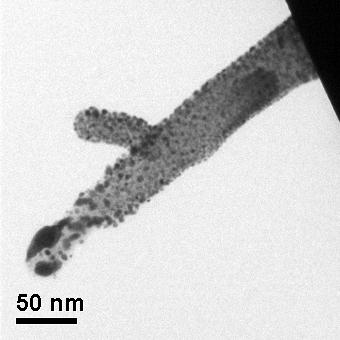
36 Gold Nanowires HRTEM [11] [11] twin [111] nanotwin 2nm 2nm [11] growth direction Average diameter: 2±5 nm One grain through the thickness A large number of twins but no dislocations Dr. C. Li In collaboration with Dr. Hsien-Hau Wang, Materials Division, Argonne National Lab
37 Tensile Stress (GPa) Tensile Stress (GPa) Tensile Yield Stress (GPa) A B C 5nm 1nm 15nm 17.5nm MD Simulations of NWs [111] Nanowires Strain nm 1nm 15nm 17.5nm [11] Nanowires Strain Diameter (nm) <111> <11> Equilibrium Strain (%) [11] [111] 1 1 (A and B) Tensile stress responses for [111] and [11] axially oriented wires (as seen in Figure 1A and 1B, respectively) with representative radii from 5nm to 17.5nm. (C) Tensile yield stress as a function of diameter for all examined sizes. Both orientations show a drop in tensile yield stress with increasing diameter Diameter (nm) [111] [11]

/atom.12.1.8.6.4.2 σ 1 =4.7.2.4.6.8.1.12.2.4.6.8.1.12 Deformation Deformation")
38 Role of Surface Defects 2 E 2 2 = E 3 ε + ξε V 3 Step is created by a ½ <11> translation; perfect dislocation shift. Orientation <111> D=5 nm Strain Rate = 5x1 7 s -1 Change in Energy (ev)/atom σ y =7.35 GPa Change in Energy (ev)/atom σ 1 = Deformation Deformation
39 Acknowledgments: Y. Zhu, Northwestern University C-H. Ke, Northwestern University N. Moldovan, Northwestern University K-H. Kim, Northwestern University B. Peng, Northwestern University T. Belytschko, Northwestern University G. Schatz, Northwestern University C. Mirkin, Northwestern University Z. Bazant, Northwestern University D. Farkas, Virginia Tech. B. Hyde, NU N. Pugno, Politecnico di Torino P. Zapol, ANL O. Auciello, ANL I. Petrov, UIUC J. Mahon, UIUC M. Marshall, UIUC B. Prorok, Aurburn University National Science Foundation-NIRT, J. Larsen-Basse, K. Chong Federal Aviation Administration, J. Newcomb NSF-NSEC at NU for Integrated Nanopatterning and Detection Technology Office of Naval Research, L. Kabakoff
Design and Operation of a MEMS-Based Material Testing System for Nanomechanical Characterization Horacio D. Espinosa, Yong Zhu, and Nicolaie Moldovan
 JOURNAL OF MICROELECTROMECHANICAL SYSTEMS, VOL. 16, NO. 5, OCTOBER 2007 1219 Design and Operation of a MEMS-Based Material Testing System for Nanomechanical Characterization Horacio D. Espinosa, Yong Zhu,
Diameter- and Loading Mode Effects of Modulus in ZnO Nanowires
 Diameter- and Loading Mode Effects of Modulus in ZnO Nanowires In Situ Measurements & Theoretical Understanding Mo-rigen H, CQ Chen, Y Shi, YS Zhang, W Zhou, JW Chen, YJ Yan, J Zhu* Beijing National Center
Effects of Defects on the Strength of Nanotubes: Experimental- Computational Comparisons
 Effects of Defects on the Strength of Nanotubes: Experimental- Computational Comparisons T. Belytschko, S. P. Xiao and R. Ruoff Department of Mechanical Engineering Northwestern University, 2145 Sheridan
Lecture 1: Introduction to NEMS
 Lecture 1: Introduction to NEMS Horacio D. Espinosa Acknowledgments: NSF-NIT, NSF-NSEC Int. Technology oadmap for Semiconductors Technology Tmi n(s) Tmax (s) CDmin (m) CDmax (m) Energy J/op Cost min $/gate
Nanomechanics Measurements and Standards at NIST
 Nanomechanics Measurements and Standards at NIST Robert F. Cook Deputy Chief, Ceramics Division Leader, Nanomechanical Properties Group robert.cook@nist.gov NIST Mission Promote U.S. innovation and industrial
EE C247B / ME C218 INTRODUCTION TO MEMS DESIGN SPRING 2016 C. NGUYEN PROBLEM SET #4
 Issued: Wednesday, March 4, 2016 PROBLEM SET #4 Due: Monday, March 14, 2016, 8:00 a.m. in the EE C247B homework box near 125 Cory. 1. This problem considers bending of a simple cantilever and several methods
Carbon Nanotubes in Interconnect Applications
 Carbon Nanotubes in Interconnect Applications Page 1 What are Carbon Nanotubes? What are they good for? Why are we interested in them? - Interconnects of the future? Comparison of electrical properties
Torsional Buckling of Double-Walled Carbon Nanotubes
 Torsional Buckling of Double-Walled Carbon Nanotubes S. H. Soong Engineering Science Programme, National University of Singapore Kent Ridge, Singapore 119260 ABSTRACT This paper is concerned with the torsional
Free Vibrations of Carbon Nanotubes with Defects
 Mechanics and Mechanical Engineering Vol. 17, No. 2 (2013) 157 166 c Lodz University of Technology Free Vibrations of Carbon Nanotubes with Defects Aleksander Muc Aleksander Banaś Ma lgorzata Chwa l Institute
Supplementary Figures
 Fracture Strength (GPa) Supplementary Figures a b 10 R=0.88 mm 1 0.1 Gordon et al Zhu et al Tang et al im et al 5 7 6 4 This work 5 50 500 Si Nanowire Diameter (nm) Supplementary Figure 1: (a) TEM image
Large scale growth and characterization of atomic hexagonal boron. nitride layers
 Supporting on-line material Large scale growth and characterization of atomic hexagonal boron nitride layers Li Song, Lijie Ci, Hao Lu, Pavel B. Sorokin, Chuanhong Jin, Jie Ni, Alexander G. Kvashnin, Dmitry
MECHANICS OF 2D MATERIALS
 MECHANICS OF 2D MATERIALS Nicola Pugno Cambridge February 23 rd, 2015 2 Outline Stretching Stress Strain Stress-Strain curve Mechanical Properties Young s modulus Strength Ultimate strain Toughness modulus
Molecular Dynamics Simulation of Fracture of Graphene
 Molecular Dynamics Simulation of Fracture of Graphene Dewapriya M. A. N. 1, Rajapakse R. K. N. D. 1,*, Srikantha Phani A. 2 1 School of Engineering Science, Simon Fraser University, Burnaby, BC, Canada
EE C247B / ME C218 INTRODUCTION TO MEMS DESIGN SPRING 2014 C. Nguyen PROBLEM SET #4
 Issued: Wednesday, Mar. 5, 2014 PROBLEM SET #4 Due (at 9 a.m.): Tuesday Mar. 18, 2014, in the EE C247B HW box near 125 Cory. 1. Suppose you would like to fabricate the suspended cross beam structure below
A Technique for Force Calibration MEMS Traceable to NIST Standards
 A Technique for Force Calibration MEMS Traceable to NIST Standards K. Abbas and Z. C. Leseman * University of New Mexico, Albuquerque, NM * Corresponding Author: MSC01-1150 Albuquerque, NM 87131: zleseman@unm.edu
December 1999 FINAL TECHNICAL REPORT 1 Mar Mar 98
 REPORT DOCUMENTATION PAGE AFRL-SR- BL_TR " Public reporting burden for this collection of information is estimated to average 1 hour per response, including the time for reviewing instruct the collection
In Situ TEM Electromechanical Testing of Nanowires and Nanotubes
 Electromechanical Analysis In Situ TEM Electromechanical Testing of Nanowires and Nanotubes Horacio D. Espinosa, * Rodrigo A. Bernal, and Tobin Filleter Material published in this Review will also appear
There's Plenty of Room at the Bottom
 There's Plenty of Room at the Bottom 12/29/1959 Feynman asked why not put the entire Encyclopedia Britannica (24 volumes) on a pin head (requires atomic scale recording). He proposed to use electron microscope
EE C245 ME C218 Introduction to MEMS Design
 EE C245 ME C218 Introduction to MEMS Design Fall 2007 Prof. Clark T.-C. Nguyen Dept. of Electrical Engineering & Computer Sciences University of California at Berkeley Berkeley, CA 94720 Lecture 12: Mechanical
Outline. 4 Mechanical Sensors Introduction General Mechanical properties Piezoresistivity Piezoresistive Sensors Capacitive sensors Applications
 Sensor devices Outline 4 Mechanical Sensors Introduction General Mechanical properties Piezoresistivity Piezoresistive Sensors Capacitive sensors Applications Introduction Two Major classes of mechanical
EE C245 ME C218 Introduction to MEMS Design
 EE C245 ME C218 Introduction to MEMS Design Fall 2007 Prof. Clark T.-C. Nguyen Dept. of Electrical Engineering & Computer Sciences University of California at Berkeley Berkeley, CA 94720 Lecture 16: Energy
Optimizing the Performance of MEMS Electrostatic Comb Drive Actuator with Different Flexure Springs
 Optimizing the Performance of MEMS Electrostatic Comb Drive Actuator with Different Flexure Springs Shefali Gupta 1, Tanu Pahwa 1, Rakesh Narwal 1, B.Prasad 1, Dinesh Kumar 1 1 Electronic Science Department,
CHAPTER 5 FIXED GUIDED BEAM ANALYSIS
 77 CHAPTER 5 FIXED GUIDED BEAM ANALYSIS 5.1 INTRODUCTION Fixed guided clamped and cantilever beams have been designed and analyzed using ANSYS and their performance were calculated. Maximum deflection
A NEW APPROACH TOWARDS PROPERTY NANOMEASUREMENTS USING IN-SITU TEM
 A NEW APPROACH TOWARDS PROPERTY NANOMEASUREMENTS USING IN-SITU TEM Z.L. WANG*, P. PONCHARAL**, W.A. DE HEER** and R.P. GAO* * School of Materials Science and Engineering, ** School of Physics, Georgia
MEMS Mechanical Fundamentals
 ROCHESTER INSTITUTE OF TECHNOLOGY MICROELECTRONIC ENGINEERING MEMS Mechanical Fundamentals Dr. Lynn Fuller webpage: http://people.rit.edu/lffeee Electrical and Microelectronic Engineering Rochester Institute
3.032 Problem Set 2 Solutions Fall 2007 Due: Start of Lecture,
 3.032 Problem Set 2 Solutions Fall 2007 Due: Start of Lecture, 09.21.07 1. In the beam considered in PS1, steel beams carried the distributed weight of the rooms above. To reduce stress on the beam, it
Bending Load & Calibration Module
 Bending Load & Calibration Module Objectives After completing this module, students shall be able to: 1) Conduct laboratory work to validate beam bending stress equations. 2) Develop an understanding of
Microstructure cantilever beam for current measurement
 264 South African Journal of Science 105 July/August 2009 Research Articles Microstructure cantilever beam for current measurement HAB Mustafa and MTE Khan* Most microelectromechanical systems (MEMS) sensors
Midterm 2 PROBLEM POINTS MAX
 Midterm 2 PROBLEM POINTS MAX 1 30 2 24 3 15 4 45 5 36 1 Personally, I liked the University; they gave us money and facilities, we didn't have to produce anything. You've never been out of college. You
Design and Analysis of Various Microcantilever Shapes for MEMS Based Sensing
 ScieTech 014 Journal of Physics: Conference Series 495 (014) 01045 doi:10.1088/174-6596/495/1/01045 Design and Analysis of Various Microcantilever Shapes for MEMS Based Sensing H. F. Hawari, Y. Wahab,
Force and Displacement Measurement
 Force and Displacement Measurement Prof. R.G. Longoria Updated Fall 20 Simple ways to measure a force http://scienceblogs.com/dotphysics/200/02/diy_force_probe.php Example: Key Force/Deflection measure
Module-4. Mechanical Properties of Metals
 Module-4 Mechanical Properties of Metals Contents ) Elastic deformation and Plastic deformation ) Interpretation of tensile stress-strain curves 3) Yielding under multi-axial stress, Yield criteria, Macroscopic
What are Carbon Nanotubes? What are they good for? Why are we interested in them?
 Growth and Properties of Multiwalled Carbon Nanotubes What are Carbon Nanotubes? What are they good for? Why are we interested in them? - Interconnects of the future? - our vision Where do we stand - our
Design of a MEMS Capacitive Comb-drive Accelerometer
 Design of a MEMS Capacitive Comb-drive Accelerometer Tolga Kaya* 1, Behrouz Shiari 2, Kevin Petsch 1 and David Yates 2 1 Central Michigan University, 2 University of Michigan * kaya2t@cmich.edu Abstract:
Platform Isolation Using Out-of-plane Compliant Mechanism
 Platform Isolation Using Out-of-plane Compliant Mechanism by Arpys Arevalo PhD Candidate in Electrical Engineering Computer, Electrical and Mathematical Sciences and Engineering (CEMSE) King Abdullah University
Gaetano L Episcopo. Scanning Electron Microscopy Focus Ion Beam and. Pulsed Plasma Deposition
 Gaetano L Episcopo Scanning Electron Microscopy Focus Ion Beam and Pulsed Plasma Deposition Hystorical background Scientific discoveries 1897: J. Thomson discovers the electron. 1924: L. de Broglie propose
EE C245 ME C218 Introduction to MEMS Design Fall 2007
 EE C245 ME C218 Introduction to MEMS Design Fall 2007 Prof. Clark T.-C. Nguyen Dept. of Electrical Engineering & Computer Sciences University of California at Berkeley Berkeley, CA 94720 Lecture 17: Energy
Experimentally Calibrating Cohesive Zone Models for Structural Automotive Adhesives
 Experimentally Calibrating Cohesive Zone Models for Structural Automotive Adhesives Mark Oliver October 19, 2016 Adhesives and Sealants Council Fall Convention contact@veryst.com www.veryst.com Outline
1. Narrative Overview Questions
 Homework 4 Due Nov. 16, 010 Required Reading: Text and Lecture Slides on Downloadable from Course WEB site: http://courses.washington.edu/overney/nme498.html 1. Narrative Overview Questions Question 1
EE C245 ME C218 Introduction to MEMS Design Fall 2010
 EE C245 ME C218 Introduction to MEMS Design Fall 2010 Prof. Clark T.-C. Nguyen Dept. of Electrical Engineering & Computer Sciences University of California at Berkeley Berkeley, CA 94720 Lecture EE C245:
Institute for Electron Microscopy and Nanoanalysis Graz Centre for Electron Microscopy
 Institute for Electron Microscopy and Nanoanalysis Graz Centre for Electron Microscopy Micromechanics Ass.Prof. Priv.-Doz. DI Dr. Harald Plank a,b a Institute of Electron Microscopy and Nanoanalysis, Graz
Mechanical Characterization of Released Thin Films by Contact
 15 Chapter 2 Mechanical Characterization of Released Thin Films by Contact Loading 2.1 Introduction The design of reliable and functional micro/nano electro mechanical systems (MEMS/NEMS) relies on the
L18: Quantized fracture mechanics of nanostructures with atomic vacancies
 L18: Quantized fracture mechanics of nanostructures with atomic vacancies 198 estimate: $10B : 4% of GDP http://www.nlm.nih.gov/medlineplus/enc y/article/000001.htm http://www.animatedteeth.com/dental_crowns/t1_dental_crow
Metallic: 2n 1. +n 2. =3q Armchair structure always metallic = 2
 Properties of CNT d = 2.46 n 2 2 1 + n1n2 + n2 2π Metallic: 2n 1 +n 2 =3q Armchair structure always metallic a) Graphite Valence(π) and Conduction(π*) states touch at six points(fermi points) Carbon Nanotube:
1.103 CIVIL ENGINEERING MATERIALS LABORATORY (1-2-3) Dr. J.T. Germaine Spring 2004 LABORATORY ASSIGNMENT NUMBER 6
 Dr. J.T. Germaine Spring 2004 LABORATORY ASSIGNMENT NUMBER 6") 1.103 CIVIL ENGINEERING MATERIALS LABORATORY (1-2-3) Dr. J.T. Germaine MIT Spring 2004 LABORATORY ASSIGNMENT NUMBER 6 COMPRESSION TESTING AND ANISOTROPY OF WOOD Purpose: Reading: During this laboratory
1.103 CIVIL ENGINEERING MATERIALS LABORATORY (1-2-3) Dr. J.T. Germaine MIT Spring 2004 LABORATORY ASSIGNMENT NUMBER 6 COMPRESSION TESTING AND ANISOTROPY OF WOOD Purpose: Reading: During this laboratory
Flexible Piezoelectric-Induced Pressure Sensors for Static. Measurements Based on Nanowires/Graphene Heterostructures
 Flexible Piezoelectric-Induced Pressure Sensors for Static Measurements Based on Nanowires/Graphene Heterostructures Zefeng Chen,, Zhao Wang,, Xinming Li,*, Yuxuan Lin, Ningqi Luo, Mingzhu Long, Ni Zhao,
E05 Resonator Design
 POLITECNICO DI MILANO MSC COURSE - MEMS AND MICROSENSORS - 2018/2019 E05 Resonator Design Giorgio Mussi 16/10/2018 In this class we will learn how an in-plane MEMS resonator handles process variabilities,
Introduction to Microeletromechanical Systems (MEMS) Lecture 9 Topics. MEMS Overview
 Lecture 9 Topics. MEMS Overview") Introduction to Microeletromechanical Systems (MEMS) Lecture 9 Topics MicroOptoElectroMechanical Systems (MOEMS) Grating Light Valves Corner Cube Reflector (CCR) MEMS Light Modulator Optical Switch Micromirrors
Introduction to Microeletromechanical Systems (MEMS) Lecture 9 Topics MicroOptoElectroMechanical Systems (MOEMS) Grating Light Valves Corner Cube Reflector (CCR) MEMS Light Modulator Optical Switch Micromirrors
Intensity (a.u.) Intensity (a.u.) Raman Shift (cm -1 ) Oxygen plasma. 6 cm. 9 cm. 1mm. Single-layer graphene sheet. 10mm. 14 cm
 Intensity (a.u.) Raman Shift (cm -1 ) Oxygen plasma. 6 cm. 9 cm. 1mm. Single-layer graphene sheet. 10mm. 14 cm") Intensity (a.u.) Intensity (a.u.) a Oxygen plasma b 6 cm 1mm 10mm Single-layer graphene sheet 14 cm 9 cm Flipped Si/SiO 2 Patterned chip Plasma-cleaned glass slides c d After 1 sec normal Oxygen plasma
Intensity (a.u.) Intensity (a.u.) a Oxygen plasma b 6 cm 1mm 10mm Single-layer graphene sheet 14 cm 9 cm Flipped Si/SiO 2 Patterned chip Plasma-cleaned glass slides c d After 1 sec normal Oxygen plasma
Chapter 7. Highlights:
 Chapter 7 Highlights: 1. Understand the basic concepts of engineering stress and strain, yield strength, tensile strength, Young's(elastic) modulus, ductility, toughness, resilience, true stress and true
Strain Measurement. Prof. Yu Qiao. Department of Structural Engineering, UCSD. Strain Measurement
 Strain Measurement Prof. Yu Qiao Department of Structural Engineering, UCSD Strain Measurement The design of load-carrying components for machines and structures requires information about the distribution
PIEZOELECTRIC TECHNOLOGY PRIMER
 PIEZOELECTRIC TECHNOLOGY PRIMER James R. Phillips Sr. Member of Technical Staff CTS Wireless Components 4800 Alameda Blvd. N.E. Albuquerque, New Mexico 87113 Piezoelectricity The piezoelectric effect is
EE C247B / ME C218 INTRODUCTION TO MEMS DESIGN SPRING 2014 PROBLEM SET #1
 Issued: Thursday, Jan. 30, 2014 PROBLEM SET #1 Due (at 9 a.m.): Wednesday Feb. 12, 2014, in the EE C247B HW box near 125 Cory. This homework assignment is intended to give you some early practice playing
Prediction of Young s Modulus of Graphene Sheets by the Finite Element Method
 American Journal of Mechanical Engineering, 15, Vol. 3, No. 6, 5-9 Available online at http://pubs.sciepub.com/ajme/3/6/14 Science and Education Publishing DOI:1.1691/ajme-3-6-14 Prediction of Young s
Ranges of Applicability for the Continuum-beam Model in the Constitutive Analysis of Carbon Nanotubes: Nanotubes or Nano-beams?
 NASA/CR-2001-211013 ICASE Report No. 2001-16 Ranges of Applicability for the Continuum-beam Model in the Constitutive Analysis of Carbon Nanotubes: Nanotubes or Nano-beams? Vasyl Michael Harik ICASE, Hampton,
International Journal of ChemTech Research CODEN (USA): IJCRGG ISSN: Vol.7, No.2, pp ,
: IJCRGG ISSN: Vol.7, No.2, pp ,") International Journal of ChemTech Research CODEN (USA): IJCRGG ISSN: 0974-4290 Vol.7, No.2, pp 678-684, 2014-2015 ICONN 2015 [4 th -6 th Feb 2015] International Conference on Nanoscience and Nanotechnology-2015
International Journal of ChemTech Research CODEN (USA): IJCRGG ISSN: 0974-4290 Vol.7, No.2, pp 678-684, 2014-2015 ICONN 2015 [4 th -6 th Feb 2015] International Conference on Nanoscience and Nanotechnology-2015
Piezoresistive Sensors
 Piezoresistive Sensors Outline Piezoresistivity of metal and semiconductor Gauge factor Piezoresistors Metal, silicon and polysilicon Close view of the piezoresistivity of single crystal silicon Considerations
Buckling of Double-walled Carbon Nanotubes
 Buckling o Double-walled Carbon anotubes Y. H. Teo Engineering Science Programme ational University o Singapore Kent idge Singapore 960 Abstract This paper is concerned with the buckling o double-walled
MOLECULAR SIMULATION FOR PREDICTING MECHANICAL STRENGTH OF 3-D JUNCTIONED CARBON NANOSTRUCTURES
 ECCM16-16 TH EUROPEAN CONFERENCE ON COMPOSITE MATERIALS, Seville, Spain, 22-26 June 214 MOLECULAR SIMULATION FOR PREDICTING MECHANICAL STRENGTH OF 3-D JUNCTIONED CARBON NANOSTRUCTURES S. Sihn a,b*, V.
MATERIALS. Why do things break? Why are some materials stronger than others? Why is steel tough? Why is glass brittle?
 MATERIALS Why do things break? Why are some materials stronger than others? Why is steel tough? Why is glass brittle? What is toughness? strength? brittleness? Elemental material atoms: A. Composition
IMPROVING FRACTURE PROPERTIES OF MEMS COMPONENTS BY SURFACE CONTROL
 IMPROVING FRACTURE PROPERTIES OF MEMS COMPONENTS BY SURFACE CONTROL A Dissertation Presented to the Faculty of the Graduate School of Cornell University in Partial Fulfillment of the Requirements for the
In situ studies on dynamic properties of carbon nanotubes with metal clusters
 In situ studies on dynamic properties of carbon nanotubes with metal clusters Jason Chang, Yuan-Chih Chang, Der-Hsien Lien, Shaw-Chieh Wang*, Tung Hsu*, and Tien T. Tsong Institute of Physics, Academia
Atomic Force Microscopy imaging and beyond
 Atomic Force Microscopy imaging and beyond Arif Mumtaz Magnetism and Magnetic Materials Group Department of Physics, QAU Coworkers: Prof. Dr. S.K.Hasanain M. Tariq Khan Alam Imaging and beyond Scanning
Lecture 19. Measurement of Solid-Mechanical Quantities (Chapter 8) Measuring Strain Measuring Displacement Measuring Linear Velocity
 Measuring Strain Measuring Displacement Measuring Linear Velocity") MECH 373 Instrumentation and Measurements Lecture 19 Measurement of Solid-Mechanical Quantities (Chapter 8) Measuring Strain Measuring Displacement Measuring Linear Velocity Measuring Accepleration and
MECH 373 Instrumentation and Measurements Lecture 19 Measurement of Solid-Mechanical Quantities (Chapter 8) Measuring Strain Measuring Displacement Measuring Linear Velocity Measuring Accepleration and
Johns Hopkins University What is Engineering? M. Karweit MATERIALS
 Why do things break? Why are some materials stronger than others? Why is steel tough? Why is glass brittle? What is toughness? strength? brittleness? Elemental material atoms: MATERIALS A. Composition
How materials work. Compression Tension Bending Torsion
 Materials How materials work Compression Tension Bending Torsion Elemental material atoms: A. Composition a) Nucleus: protons (+), neutrons (0) b) Electrons (-) B. Neutral charge, i.e., # electrons = #
EE C245 ME C218 Introduction to MEMS Design
 EE C245 ME C218 Introduction to MEMS Design Fall 2007 Prof. Clark T.-C. Nguyen Dept. of Electrical Engineering & Computer Sciences University of California at Berkeley Berkeley, CA 94720 ecture 15: Beam
ME 243. Mechanics of Solids
 ME 243 Mechanics of Solids Lecture 2: Stress and Strain Ahmad Shahedi Shakil Lecturer, Dept. of Mechanical Engg, BUET E-mail: sshakil@me.buet.ac.bd, shakil6791@gmail.com Website: teacher.buet.ac.bd/sshakil
[5] Stress and Strain
![[5] Stress and Strain](/thumbs/95/123344550.jpg "[5] Stress and Strain") [5] Stress and Strain Page 1 of 34 [5] Stress and Strain [5.1] Internal Stress of Solids [5.2] Design of Simple Connections (will not be covered in class) [5.3] Deformation and Strain [5.4] Hooke s Law
[5] Stress and Strain Page 1 of 34 [5] Stress and Strain [5.1] Internal Stress of Solids [5.2] Design of Simple Connections (will not be covered in class) [5.3] Deformation and Strain [5.4] Hooke s Law
Mechanical Characterization of High Aspect Ratio Silicon Nanolines
 Mater. Res. Soc. Symp. Proc. Vol. 1086 2008 Materials Research Society 1086-U05-07 Mechanical Characterization of High Aspect Ratio Silicon Nanolines Bin Li 1, Huai Huang 1, Qiu Zhao 1, Zhiquan Luo 1,
Scattering-type near-field microscopy for nanoscale optical imaging
 Scattering-type near-field microscopy for nanoscale optical imaging Rainer Hillenbrand Nano-Photonics Group Max-Planck-Institut für Biochemie 82152 Martinsried, Germany Infrared light enables label-free
EE C245 ME C218 Introduction to MEMS Design Fall 2012
 EE C245 ME C218 Introduction to MEMS Design Fall 2012 Prof. Clark T.-C. Nguyen Dept. of Electrical Engineering & Computer Sciences University of California at Berkeley Berkeley, CA 94720 Lecture EE C245:
EE C245 ME C218 Introduction to MEMS Design
 EE C245 ME C218 Introduction to MEMS Design Fall 2007 Prof. Clark T.-C. Nguyen Dept. of Electrical Engineering & Computer Sciences University of California at Berkeley Berkeley, CA 94720 Lecture 23: Electrical
Analysis of Stress Distribution in Piezoelectric. MEMS Energy Harvester Using Shaped Cantilever Structure
 Analysis of Stress Distribution in Piezoelectric MEMS Energy Harvester Using Shaped Cantilever Structure Jung-Hyun Park 1, Jun-Seok Kang 2, Ho-Sang Ahn 1, Seon-Bae Kim 1, Dan Liu 1, AND Dong-Joo Kim 1
NORMAL STRESS. The simplest form of stress is normal stress/direct stress, which is the stress perpendicular to the surface on which it acts.
 NORMAL STRESS The simplest form of stress is normal stress/direct stress, which is the stress perpendicular to the surface on which it acts. σ = force/area = P/A where σ = the normal stress P = the centric
Chapter 10. Nanometrology. Oxford University Press All rights reserved.
 Chapter 10 Nanometrology Oxford University Press 2013. All rights reserved. 1 Introduction Nanometrology is the science of measurement at the nanoscale level. Figure illustrates where nanoscale stands
III-V nanostructured materials synthesized by MBE droplet epitaxy
 III-V nanostructured materials synthesized by MBE droplet epitaxy E.A. Anyebe 1, C. C. Yu 1, Q. Zhuang 1,*, B. Robinson 1, O Kolosov 1, V. Fal ko 1, R. Young 1, M Hayne 1, A. Sanchez 2, D. Hynes 2, and
Frictional characteristics of exfoliated and epitaxial graphene
 Frictional characteristics of exfoliated and epitaxial graphene Young Jun Shin a,b, Ryan Stromberg c, Rick Nay c, Han Huang d, Andrew T. S. Wee d, Hyunsoo Yang a,b,*, Charanjit S. Bhatia a a Department
STRAIN GAUGES YEDITEPE UNIVERSITY DEPARTMENT OF MECHANICAL ENGINEERING
 STRAIN GAUGES YEDITEPE UNIVERSITY DEPARTMENT OF MECHANICAL ENGINEERING 1 YEDITEPE UNIVERSITY ENGINEERING FACULTY MECHANICAL ENGINEERING LABORATORY 1. Objective: Strain Gauges Know how the change in resistance
Chapter 9. Electron mean free path Microscopy principles of SEM, TEM, LEEM
 Chapter 9 Electron mean free path Microscopy principles of SEM, TEM, LEEM 9.1 Electron Mean Free Path 9. Scanning Electron Microscopy (SEM) -SEM design; Secondary electron imaging; Backscattered electron
Lecture 4 Honeycombs Notes, 3.054
 Honeycombs-In-plane behavior Lecture 4 Honeycombs Notes, 3.054 Prismatic cells Polymer, metal, ceramic honeycombs widely available Used for sandwich structure cores, energy absorption, carriers for catalysts
Abstract. 1 Introduction
 In R. A. Adey et al., eds., Simulation and Design of Microsystems and Microstructures (Proceedings of the 1st International Conference on Simulation and Design of Microsystems and Microstructures), Computational
Frontiers of Fracture Mechanics. Adhesion and Interfacial Fracture Contact Damage
 Frontiers of Fracture Mechanics Adhesion and Interfacial Fracture Contact Damage Biology, Medicine & Dentistry The Next Frontiers For Mechanics One of the current challenges in materials & mechanics is
Microelectromechanical systems (MEMS) have become an increasingly important area of
 have become an increasingly important area of") 1 Chapter 1 Introduction 1.1 Background Microelectromechanical systems (MEMS) have become an increasingly important area of technology. This is due to the premise that the efficiencies of high volume production
1 Chapter 1 Introduction 1.1 Background Microelectromechanical systems (MEMS) have become an increasingly important area of technology. This is due to the premise that the efficiencies of high volume production
19 Mechanics of Carbon Nanotubes 1
 19 Mechanics of Carbon Nanotubes 1 Dong Qian Northwestern University Gregory J. Wagner Northwestern University Wing Kam Liu Northwestern University Min-Feng Yu University of Illinois Rodney S. Ruoff Northwestern
Learning Objectives By the end of this section, the student should be able to:
 Mechanics of Materials stress and strain flexural l beam bending analysis under simple loading conditions EECE 300 011 1 Learning Objectives By the end of this section, the student should be able to: describe
Supplementary Figure S1. AFM images of GraNRs grown with standard growth process. Each of these pictures show GraNRs prepared independently,
 Supplementary Figure S1. AFM images of GraNRs grown with standard growth process. Each of these pictures show GraNRs prepared independently, suggesting that the results is reproducible. Supplementary Figure
ETH Rüschlikon the people and their research
 ETH Zurich @ Rüschlikon the people and their research Prof. Dr. Dimos Poulikakos, Laboratory of Thermodynamics in Emerging Technologies and Coordinator of the Nanotechnology Center, ETH Zurich The Vision
MEMS Report for Lab #3. Use of Strain Gages to Determine the Strain in Cantilever Beams
 MEMS 1041 Report for Lab #3 Use of Strain Gages to Determine the Strain in Cantilever Beams Date: February 9, 2016 Lab Instructor: Robert Carey Submitted by: Derek Nichols Objective: The objective of this
EE C245 ME C218 Introduction to MEMS Design Fall 2007
 EE C245 ME C218 Introduction to MEMS Design Fall 2007 Prof. Clark T.-C. Nguyen Dept. of Electrical Engineering & Computer Sciences University of California at Berkeley Berkeley, CA 94720 Lecture 13: Material
PY5020: Nanomechanics Nanoscience MEMS and NEMS
 PY5020: Nanomechanics Nanoscience MEMS and NEMS Toby Hallam hallamt@tcd.ie Overview - MEMS (Micro-Electro-Mechanical Systems) - Some enabling technologies RIE CPD - Capacitive actuators Pull-in instability
Today s Presentation
 Today s Presentation MEMS Comb Drive Actuator to Vary Tension & Compression of a Resonating Nano-Doubly Clamped Beam for High-Resolution & High Sensitivity Mass Detection Adam Hurst 1 John Regis 1 Chou
EECS C245 ME C218 Midterm Exam
 University of California at Berkeley College of Engineering EECS C245 ME C218 Midterm Eam Fall 2003 Prof. Roger T. Howe October 15, 2003 Dr. Thara Srinivasan Guidelines Your name: SOLUTIONS Circle your
COMSOL Simulation of a Dualaxis MEMS Accelerometer with T-shape Beams
 COMSOL Simulation of a Dualaxis MEMS Accelerometer with T-shape Beams Ce Zheng 1, Xingguo Xiong 2, Junling Hu 3, 1 Department of Electrical Engineering, University of Bridgeport, Bridgeport, CT, USA 2
Micro Chemical Vapor Deposition System: Design and Verification
 Micro Chemical Vapor Deposition System: Design and Verification Q. Zhou and L. Lin Berkeley Sensor and Actuator Center, Department of Mechanical Engineering, University of California, Berkeley 2009 IEEE
Carbon Nanotube Thin-Films & Nanoparticle Assembly
 Nanodevices using Nanomaterials : Carbon Nanotube Thin-Films & Nanoparticle Assembly Seung-Beck Lee Division of Electronics and Computer Engineering & Department of Nanotechnology, Hanyang University,
EE C245 - ME C218 Introduction to MEMS Design Fall Today s Lecture
 EE C45 - ME C8 Introduction to MEMS Design Fall 3 Roger Howe and Thara Srinivasan Lecture 9 Energy Methods II Today s Lecture Mechanical structures under driven harmonic motion develop analytical techniques
1 332 Laboratories 1. 2 Computational Exercises 1 FEA of a Cantilever Beam... 1 Experimental Laboratory: Tensile Testing of Materials...
 1 332 Laboratories Contents 1 332 Laboratories 1 2 Computational Exercises 1 FEA of a Cantilever Beam.......................................... 1 Experimental Laboratory: Tensile Testing of Materials..........................
Characterization of MEMS Devices
 MEMS: Characterization Characterization of MEMS Devices Prasanna S. Gandhi Assistant Professor, Department of Mechanical Engineering, Indian Institute of Technology, Bombay, Recap Fabrication of MEMS Conventional
Characterization of MEMS Devices
 MEMS: Characterization Characterization of MEMS Devices Prasanna S. Gandhi Assistant Professor, Department of Mechanical Engineering, Indian Institute of Technology, Bombay, Recap Characterization of MEMS