Valleytronic Properties in 2D materials
|
|
|
- Owen McGee
- 5 years ago
- Views:
Transcription

1 MPI-UBC-UT Winter School on Quantum Materials Valleytronic Properties in 2D materials Feb 16, 2018 University of Tokyo Yoshi Iwasa, Univ. Tokyo & RIKEN
 High magnetic field measurements Y. Kohama, M. Tokunaga (ISSP) Theory T. Oka (Dresden), M. S. Bahramy (Tokyo), Y.")
2 Acknowledgements Univ Tokyo, Iwasa group SARPES M. Sakano, K. Ishizaka (Tokyo), S. Shin, K. Yaji (ISSP), K. Miyamoto, T. Okuda (Hiroshima) High magnetic field measurements Y. Kohama, M. Tokunaga (ISSP) Theory T. Oka (Dresden), M. S. Bahramy (Tokyo), Y. Yanase Y. Nakamura (Kyoto)
3 Contents 1. Introduction 2D materials Valley degree of freedom in TMDs 2. Valleytronics Valley Hall effect Circularly polarized light source 3. Superconductivity with spin-valley locking Enhanced Hc2 by SOI

")


4 2D Electron Systems insulator semiconductor metal n 2D (cm 2 ) He surface Interface (GaAs/AlGaAs) Si MOS-FET microwave-photons-nul


5 2D Electron Systems 2D Materials 2D crystal Interfaces (LAO/STO FeSe/STO) Electrochemical Interfaces Scotch Tape MBE electrolyte CVD
 0 ev")
 0.6~2.")


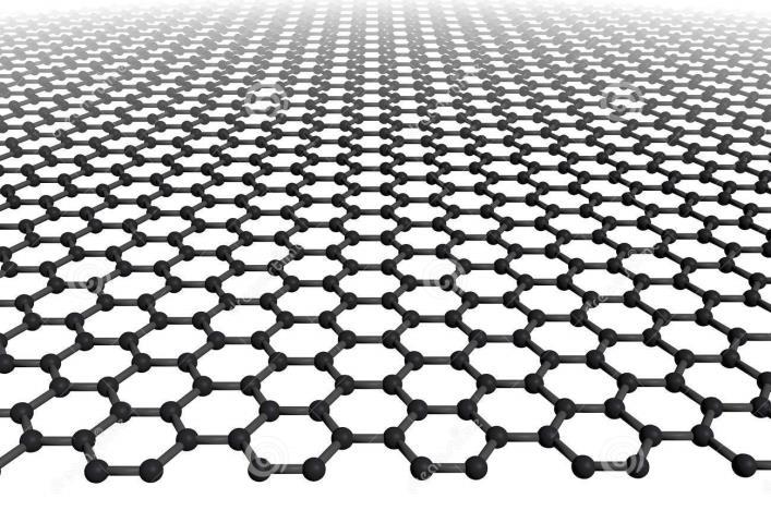
6 Family of 2D crystalline systems E g ( ev ) 0 ev ~2 ev (monolayer) ~0.3 ev (bulk) 0.6~2.3 ev depending on # of layers 7.2 ev (indirect) Graphene Black Phosphorus TMD (MX2) h-bn M: Mo, W, Ta, X:S, Se, Te
7 Valleytronics Valley: as information carriers Candidate materials: Si Diamond, AlAs Bi graphene Challenge: Search for valley selective external perturbation
")
8 Normalized Direct gap in monolayer MoS 2 Bulk 4-layer 2-layer Monolayer Direct gap (±K) Indirect gap Splendiani et al., Nano Lett. (2010) Cao et al., Nat. Comm. (2012) Mak et al., Phys. Rev. Lett. (2010)
 Graphene TMD")
")
")
 Light")
 Laser")
9 Transition Metal Dichalcogenides (TMD, MX 2 ) Graphene TMD Monolayer Isolation (PNAS 2005) Photoluminescence (PRL 2010) Monolayer FET(NNano 2011) Valleytronics (NNano 2012) Superconductivity (Science 2012) Photodetectors (NNano 2013) Light Emitting Diodes (Science 2014) Piezoelectic (Nature 2014) Laser (Nature 2015) Thermolelectrics (2015)


10 Honeycomb lattice with broken inversion symmetry Graphene TMDs Massless Dirac fermion at ±K Massive Dirac fermion at ±K H = 0 γ τq x + iq y γ τq x iq y 0 H = Δ 2 γ τq x + iq y γ τq x iq y Δ 2

11 Valley dependent optical selection rules j z j z = 11± 1 j z j= z = j z j z = j z j z = ± Xiao et al. Phys. Rev. Lett. (2012) Large spin-orbit interaction Schematic of effective magnetic field
12 Circularly polarized Photoluminescence s - excitation Excitation by circularly polarized laser Selective detection of σ ± component s - s + η = I + I I + + I Cao et al., Nat. Comm. (2012) Zeng et al., Nat. Nano. (2012) Mak et al., Nat. Nano. (2012) Sallen et al., Phys. Rev. B (2012) WSe 2 MoSe 2 MoS 2 WS 2 PL 63 % 5 % 56 % 42 %

13 Spin-valley locking Broken inversion symmetry Spin-Orbit Interaction Spin-resolved ARPES B eff p E int D. Xiao et al., PRL 108, (2012)

")


")


14 Monolayer vs. Bulk 1ML MoS 2 (P6m2) 2H-MoS 2 (P6 3 /mmc) Bulk 3R-MoS 2 (R3m) 3-fold S Mo S K K 6-fold Noncentrosymmetric Centrosymmetric K K 3-fold Noncentrosymmetric Spin-Valley coupling in bulk
 R. Suzuki et al., Nat Nano 9, 611 (2014). P. King s group, Nat Phys 10, 385 (2014).")
15 Spin-valley locking Broken inversion symmetry Spin-Orbit Interaction Spin-resolved ARPES B eff p E int D. Xiao et al., PRL 108, (2012) R. Suzuki et al., Nat Nano 9, 611 (2014). P. King s group, Nat Phys 10, 385 (2014).
. K. F. Mak et al., Nat Nano 7, 494 (2012).")
 Y. J. Zhang et al.")
. J. Lee et al., Nat Nano 11, 421 (2016).")
. A. Srivastava et al.")
16 Progress of valleytronics in monolayer TMDs Circular dichroic PL H. Zeng et al., Nat Nano 7, 490 (2012). K. F. Mak et al., Nat Nano 7, 494 (2012). T. Cao et al., Nat. Comm. 3, 887 (2012). EO conversion (valley light emitting transistor) Y. J. Zhang et al., Science 344, 725 (2014). σ -K K σ + OE conversion (valley Hall effect) K. F. Mak et al. Science 344, 1489 (2014). J. Lee et al., Nat Nano 11, 421 (2016). Magneto-optics (valley Zeeman effect) L. Li et al., PRL 113, (2014). D. MacNeil et al., PRL 114, (2015). A. Srivastava et al., Nat Phys 11, 141 (2015). G. Aivasian et al., Nat Phys 11, 148 (2015).
17 Berry curvature in monolayer MoS2 :wave vector :Bloch function T. Cao et al., Nat. Comm. 2, 887 (2012)

18 Hall effect Hall effect Spontaneous Hall effect External magnetic field Internal magnetic field By external magnetic fields WIthout ernal magnetic fields 18
19 Spontaneous Hall effect Various Hall effect Theory electron / hole phonon spin valley magnon exciton optical response composite particles Anomalous velocity 1 E( k) 1 r ( r) Ωk ( ) k Potential gradient e.g. electric fields E Berry curvature internal magnetic field Hall effect of excitons??? Exciton with finite Berry curvature W. Yao et al., Phys. Rev. Lett. 101, (2008). S. I. Kuga et al., Phys. Rev. B 78, (2008). Candidate: Valley excitons in TMDs!! 19
20 Valley Hall Effect in TMD monolayer 1 E( k) 1 r ( r) Ωk ( ) k Potential gradient e.g. electric fields E Berry curvature effective magnetic field J. Lee et al., Nature Nano 11, 421 (2016) K. F. Mak et al. Science 344, 1489 (2014)

 k σ + σ - K. F. Mak et al.")
21 Valley Hall effect in monolayer MoS2 Electrical detection of the optically excited electrons and holes 1 E( k) 1 r ( r) Ωk ( ) k σ + σ - K. F. Mak et al. Science 344, 1489 (2014)

")
22 Valley Hall effect in monolayer MoS2 Carrier doping by back gating Detection of the accumulated spins at the edge by Kerr rotation 1 E( k) 1 r ( r) Ωk ( ) k J. Lee, K. F. Mak et al., Nature Nano 11, 421 (2016)
 Ωk ( ) k Potential gr")

 K. F. Mak et al.")
23 Valley Hall Effect in TMD monolayer 1 E( k) 1 r ( r) Ωk ( ) k Potential gradient e.g. electric fields E Berry curvature effective magnetic field J. Lee et al., Nature Nano 11, 421 (2016) K. F. Mak et al. Science 344, 1489 (2014) Theory of valley-nernst effect S. Konabe et al. PRB 90, (2014).
 K. F.")
24 Valley Hall Effect in TMD monolayer 1 E( k) 1 r ( r) Ωk ( ) k Potential gradient e.g. electric fields E Berry curvature effective magnetic field J. Lee et al., Nature Nano 11, 421 (2016) K. F. Mak et al. Science 344, 1489 (2014) Exciton Hall effect
. two-dimensionality direct gap semiconductor K. F. Mak et al., Nat. Mat. 12, 207 (2013).")
25 Exciton in monolayer TMDs Transition metal dichalcogenides Mo S Absorption spectrum E gap excitonic states 200 mev Z. Y. Zhu et al., PRB 84, (2011). two-dimensionality direct gap semiconductor K. F. Mak et al., Nat. Mat. 12, 207 (2013). stable excitons 25


26 PL mapping in monolayer MoS2
 (under B = 0 ) 1")
27 Observation of exciton Hall effect Polarization-resolved PL mapping(pumped by linearly polarized light) (under B = 0 ) 1 mm
 I I I s s (under B = 0")
28 Observation of exciton Hall effect Polarization-resolved PL mapping(pumped by linearly polarized light) I I I s s (under B = 0 ) -3 3


29 Trajectories of Hall effect Color mapping of I 1 Conventional Hall effect 0 h e - -1 Hall effect of excitons, visible objects. Tracing trajectories M. Onga et al., Nature Materials 16, 1193 (2017)
.")
30 Hall angle of exciton hall effect Definition & evaluation Lxy EHE L xx Large Hall angle ( real space observation) L xy L xx Sample dependence # EHE cf. Valley Hall Effect 10 3 K. F. Mak et al., Science 344, 1489 (2014). Trion Exciton Internal structure of composite particles likely result in the large and non-trivial Berry curvature (due to exchange interaction). H. Yu et al., Nat. Comm. 5, 3876 (2014). Due to the Bose nature of exciton, the valley conductivity can be orders of magnitude larger than the Fermi one. T. Yu and M. W. Wu, PRB 93, (2016)
 FET Electric Double Layer")

31 FET and EDLT (Electric Double Layer Transistor) FET Electric Double Layer Transistor (EDLT) Insulator Semiconductor Metal Electronic phase transitions
32 TMD-EDLT FET vs EDLT (WSe 2 ) S D Carrier density (WSe 2 ) EDLT 220K I DS (A) FET I DS (A) MoS 2 WSe 2 n 2D (x10 13 /cm 2 ) V G (V) V G (V) V G (V) SiO 2 (Novoselov et al., PNAS (2005)) HfO 2 (Radsavljevic et al., Nat. Nano. (2011)) EDL (Zhang et al., Nano Lett. (2012))
 20 10 0 0 2.0 1 2 V DS (V) 3 4 V 4T (V) 1.5 1.0 0.5 S V V V D 0.")
33 Field-induced p-i-n Junction Output curve 40 V G G = = 22 V Cool down here 30 I DS (ma) V DS (V) 3 4 V 4T (V) S V V V D V DS (V)
 15 10 5 220 K 150 K 0-3 -2-1 0 1 2")
 Hall effect measurement R H1 R H2 500")
 0 R H2 ( ) 0-500")
34 Field-induced p-i-n Junction 20 Output curve I DS (ma) K 150 K V DS (V) Zhang et al., Nano Lett. (2013) Hall effect measurement R H1 R H /cm /cm 2 R H1 ( ) 0 R H2 ( ) B (T) B (T)

 24 18 12 6 0 0 5 10 15 Bias current (ma) Bias Absorption PL intensity")
35 Electroluminescence from WSe 2 Au/Ti 5 μm EL intensity (a.u.) Bias current (ma) Bias Absorption PL intensity A-exciton B-exciton RT He et al., PRL (2014) RT excitation 2.33 ev 100 K 6V 5V 4V 3V 2V EL intensity Photon energy (ev) 100 K 2.2 Y. J. Zhang et al., Science 344, 725 (2014)
 s- s+ 1.")
 Simultaneous publications SiN gating:")
 HfO 2 gating: Baugher et al. Nat. Nano.")
36 Electroluminescence from WSe 2 Current-induced circularly polarized EL 40 K EDL gating EL intensity (a.u.) s- s Photon energy (ev) Y. J. Zhang et al. Science (2014) Simultaneous publications SiN gating: Pospischil et al. Nat. Nano. (2014) HfO 2 gating: Baugher et al. Nat. Nano. (2014) hbn gating: Ross et al. Nat. Nano. (2014)
37 Electronic structure of gated multilayer MoS n(z) Real space (SC state) Quasi-monolayer SC z E Gated multilayer is a mimic of monolayer H. T. Yuan et al., Nat Phys (2013) M. S. Bahramy T. Brumme et al.. Phys. Rev. B 91, (2015)


38 Electrical Control of Circular Polarization Field-effect doping is reversible and tunable Modulation of diode profile WSe K Circularly polarized light source showing electrical controllability Y. J. Zhang et al. Science (2014)

 1.60 M.")
39 Circularly Polarized EL from MoSe 2 6 K MoSe K EL intensity (a.u.) Photon energy (ev) 1.60 M. Onga, et al. APL (2016).


40 Optical filter Helical Light Generation Angular momentum selection rule Spin LED Valley LET Structure Konishi et al., PRL. (2011) Yang et al., Adv. Mater. (2013) Helicity control needs spin (External magnetic field) Helicity can be controlled by current (External in-plane electric field)
 10 4")

41 Gate induced superconductivity in MoS V EDLT =0V 10 5 R s ( ) V EDLT =6V T (K) J. T. Ye et al. Science 338, 1193 (2012)
 Nature Phys. 6, 104 (2010). PRL 107, 207001 (2011). Tl-Pb single layer (1L) PRL 115, 147003 (2015). FeSe-1L CPL 29, 03742 (2012).")
. Nature Nanotech. 10, 765 (2015). intercalated graphene PNAS 112, 11795 (2015). ACS Nano 10, 2761 (2016).")
. Science 350, 409 (2015). TMDCs-quasi-1L Science 338, 1193 (2012). Sci. Rep. 5, 12534 (2015). Nature Nano. 11, 339 (2016).")
42 MBE (layer-by-layer growth) Newly emerging 2D superconductors CVD mechanically-exfoliated (2D crystals) Ionic gating (EDLT) Pb, In single layer (1L) Nature Phys. 6, 104 (2010). PRL 107, (2011). Tl-Pb single layer (1L) PRL 115, (2015). FeSe-1L CPL 29, (2012). Heavy Fermion superlattice Nature Phys. 7, 849 (2011). Mo 2 C-1~2L Nature Mat. 14, 1135 (2015). BSCCO-1L Nature Comm. 5, 5708 (2014). NbSe 2-1L Nano Letter 15, 4914 (2015). Nature Nanotech. 10, 765 (2015). intercalated graphene PNAS 112, (2015). ACS Nano 10, 2761 (2016). STO & KTO Nature Mat 7, 855 (2008). Nature Nano. 6, 408 (2011). Cuprate (LSCO) Nature 472, 458 (2011). ZrNCl-quasi-1L Nature Mat. 9, 1314 (2010). Science 350, 409 (2015). TMDCs-quasi-1L Science 338, 1193 (2012). Sci. Rep. 5, (2015). Nature Nano. 11, 339 (2016). Nature Phys. 12, 144 (2016).

43 2D superconductors Y. Saito et al. Nature Reviews Materials 2, (2016)
 (broken inversion symmetry) Quantum")
 Nonreciprocal Supercurrent Wakatsuki/Saito, Sci Adv (2017) Qin, Nat Comm")
44 EDLT: New platform of 2D superconductivity (materials) SrTiO 3, KTaO 3, LSCO, YBCO ZrNCl, MoS 2, MoSe 2, TiSe 2, FeSe, (weak pinning) (broken inversion symmetry) Quantum Phase Transition Saito, Science (2015), Nat Comm (2018) Enhanced Hc2 by SOI Saito, Nat Phys (2016) Nonreciprocal Supercurrent Wakatsuki/Saito, Sci Adv (2017) Qin, Nat Comm (2017)


45 Noncentrosymmetric superconductors Rashba-type spin polarization Parity mixture CePt3Si CeRhSi3, CeIrSi3, Uir, Li2Pt3B, Li2Pd3B, Benchmark; Enhanced Pauli limit P H c 2 To observe Pauli limit, Maki parameter Two ways Heavy electron mass Reduced dimensions 2 H 2 1 H orb c P c2
 Quasi-monolayer SC DFT calculation~ 1 layer Brumme et al., PRB 91, 155436 (2015).")
46 Monolayer MoS 2 ; a new class of noncentrosymmetric SC Trigonal structure with simple band structure with out-of-plane spin polarization n(z) Quasi-monolayer SC DFT calculation~ 1 layer Brumme et al., PRB 91, (2015). z 2H-type structure E


47 R-T Curves for H and H // (MoS 2 ) c q H H H

 15 10 H H H c2// ( T ) 12 0 2")
 ) 1/ 2")

48 Thickness of superconductivity in MoS 2 -EDLT 20 Pauli limit 2D Tinkam model H c2 ( T ) GL (0) (1 T / T c ) B c2 (T) H H H c2// ( T ) (0) d GL d SC 1.4 nm sc (1 T / T c ( 0 = h/2e) ) 1/ 2 5 GL (0) 8.1 nm T (K) Cf. EDA monolayer T. Brumme et al., PRB91, (2015).
49 High field measurement at ISSP, Univ Tokyo on gated MoS 2 H Experiment 2D GL (orbital limit) Enhanced Pauli limit conventional Pauli limit Y. Saito et al., Nature Physics 12, 144 (2016).
 = 13 mev Intervalley pairing s + f")
50 Zero-field Zeeman splitting in conduction band in gated MoS 2 M. S. Bahramy Zeeman splitting (E F ) = 13 mev Intervalley pairing s + f symmetry FFLO
 Y. Saito et al. Nature Phys. 12, 144 (2016) J. M. Lu et al. Science.")
51 H Comparison with Theory for MoS 2 Experiment Theory (Pauli limit) 2D GL (orbital limit) Rashba Zeeman Enhanced Pauli limit conventional Pauli limit M. S. Bahramy Y. Nakamura and Y. Yanase H c2 : semiquantitatively explained by Zeeman type spin-valley locking Further theory Ilic et al.. PRL 119, (2017) Y. Saito et al. Nature Phys. 12, 144 (2016) J. M. Lu et al. Science. 350, 1353 (2015) X. Xi et al. Nature Phys. 12, 139 (2016)

52 Summary: Valleytronic Properties of 2D materials 1. Introduction 2. Exciton Hall effect 3. Valley Light Emitting Transistor 4. 2D superconductivity Enhanced Hc2 by SOI
Chiral electroluminescence from 2D material based transistors
 New Perspectives in Spintronic and Mesoscopic Physics (NPSMP2015) June 10-12, 2015 Kashiwanoha, Japan Chiral electroluminescence from 2D material based transistors Y. Iwasa University of Tokyo & RIKEN
Fermi polaron-polaritons in MoSe 2
 Fermi polaron-polaritons in MoSe 2 Meinrad Sidler, Patrick Back, Ovidiu Cotlet, Ajit Srivastava, Thomas Fink, Martin Kroner, Eugene Demler, Atac Imamoglu Quantum impurity problem Nonperturbative interaction
SUPPLEMENTARY INFORMATION
 In the format provided by the authors and unedited. DOI: 10.1038/NMAT4996 Exciton Hall effect in monolayer MoS2 Masaru Onga 1, Yijin Zhang 2, 3, Toshiya Ideue 1, Yoshihiro Iwasa 1, 4 * 1 Quantum-Phase
Valley Hall effect in electrically spatial inversion symmetry broken bilayer graphene
 NPSMP2015 Symposium 2015/6/11 Valley Hall effect in electrically spatial inversion symmetry broken bilayer graphene Yuya Shimazaki 1, Michihisa Yamamoto 1, 2, Ivan V. Borzenets 1, Kenji Watanabe 3, Takashi
Dirac matter: Magneto-optical studies
 Dirac matter: Magneto-optical studies Marek Potemski Laboratoire National des Champs Magnétiques Intenses Grenoble High Magnetic Field Laboratory CNRS/UGA/UPS/INSA/EMFL MOMB nd International Conference
Monolayer Semiconductors
 Monolayer Semiconductors Gilbert Arias California State University San Bernardino University of Washington INT REU, 2013 Advisor: Xiaodong Xu (Dated: August 24, 2013) Abstract Silicon may be unable to
Valley Zeeman Effect of free and bound excitons in WSe2
 Valley Zeeman Effect of free and bound excitons in WSe2 Ajit Srivastava Quantum Photonics Group ETH Zurich, Switzerland 24.01.2014 TMD Research Motivation Optical control of spins & pseudo-spins 2D optical
Center for Integrated Nanostructure Physics (CINAP)
") Center for Integrated Nanostructure Physics (CINAP) - Institute for Basic Science (IBS) was launched in 2012 by the Korean government to promote basic science in Korea - Our Center was established in 2012
Center for Integrated Nanostructure Physics (CINAP) - Institute for Basic Science (IBS) was launched in 2012 by the Korean government to promote basic science in Korea - Our Center was established in 2012
2D MBE Activities in Sheffield. I. Farrer, J. Heffernan Electronic and Electrical Engineering The University of Sheffield
 2D MBE Activities in Sheffield I. Farrer, J. Heffernan Electronic and Electrical Engineering The University of Sheffield Outline Motivation Van der Waals crystals The Transition Metal Di-Chalcogenides
vapour deposition. Raman peaks of the monolayer sample grown by chemical vapour
 Supplementary Figure 1 Raman spectrum of monolayer MoS 2 grown by chemical vapour deposition. Raman peaks of the monolayer sample grown by chemical vapour deposition (S-CVD) are peak which is at 385 cm
Physics in two dimensions in the lab
 Physics in two dimensions in the lab Nanodevice Physics Lab David Cobden PAB 308 Collaborators at UW Oscar Vilches (Low Temperature Lab) Xiaodong Xu (Nanoscale Optoelectronics Lab) Jiun Haw Chu (Quantum
Supporting information. Gate-optimized thermoelectric power factor in ultrathin WSe2 single crystals
 Supporting information Gate-optimized thermoelectric power factor in ultrathin WSe2 single crystals Masaro Yoshida 1, Takahiko Iizuka 1, Yu Saito 1, Masaru Onga 1, Ryuji Suzuki 1, Yijin Zhang 1, Yoshihiro
Phase Change and Piezoelectric Properties of Two-Dimensional Materials
 Phase Change and Piezoelectric Properties of Two-Dimensional Materials April 22, 2015 Karel-Alexander Duerloo, Yao Li, Yao Zhou, Evan Reed Department of Materials Science and Engineering Stanford University
Supplementary Information for Atomically Phase-Matched Second-Harmonic Generation. in a 2D Crystal
 Supplementary Information for Atomically Phase-Matched Second-Harmonic Generation in a 2D Crystal Mervin Zhao 1, 2, Ziliang Ye 1, 2, Ryuji Suzuki 3, 4, Yu Ye 1, 2, Hanyu Zhu 1, Jun Xiao 1, Yuan Wang 1,
Electron spins in nonmagnetic semiconductors
 Electron spins in nonmagnetic semiconductors Yuichiro K. Kato Institute of Engineering Innovation, The University of Tokyo Physics of non-interacting spins Optical spin injection and detection Spin manipulation
2D Materials with Strong Spin-orbit Coupling: Topological and Electronic Transport Properties
 2D Materials with Strong Spin-orbit Coupling: Topological and Electronic Transport Properties Artem Pulkin California Institute of Technology (Caltech), Pasadena, CA 91125, US Institute of Physics, Ecole
single-layer transition metal dichalcogenides MC2
 single-layer transition metal dichalcogenides MC2 Period 1 1 H 18 He 2 Group 1 2 Li Be Group 13 14 15 16 17 18 B C N O F Ne 3 4 Na K Mg Ca Group 3 4 5 6 7 8 9 10 11 12 Sc Ti V Cr Mn Fe Co Ni Cu Zn Al Ga
TOPOLOGICAL BANDS IN GRAPHENE SUPERLATTICES
 TOPOLOGICAL BANDS IN GRAPHENE SUPERLATTICES 1) Berry curvature in superlattice bands 2) Energy scales for Moire superlattices 3) Spin-Hall effect in graphene Leonid Levitov (MIT) @ ISSP U Tokyo MIT Manchester
Dynamics of electrons in surface states with large spin-orbit splitting. L. Perfetti, Laboratoire des Solides Irradiés
 Dynamics of electrons in surface states with large spin-orbit splitting L. Perfetti, Laboratoire des Solides Irradiés Outline Topology of surface states on the Bi(111) surface Spectroscopy of electronic
Ferromagnetism and Anomalous Hall Effect in Graphene
 Ferromagnetism and Anomalous Hall Effect in Graphene Jing Shi Department of Physics & Astronomy, University of California, Riverside Graphene/YIG Introduction Outline Proximity induced ferromagnetism Quantized
Generation and electric control of spin valleycoupled circular photogalvanic current in WSe 2
 Generation and electric control of spin valleycoupled circular photogalvanic current in WSe 2 1. Electronic band structure of WSe 2 thin film and its spin texture with/without an external electric field
Surface Majorana Fermions in Topological Superconductors. ISSP, Univ. of Tokyo. Nagoya University Masatoshi Sato
 Surface Majorana Fermions in Topological Superconductors ISSP, Univ. of Tokyo Nagoya University Masatoshi Sato Kyoto Tokyo Nagoya In collaboration with Satoshi Fujimoto (Kyoto University) Yoshiro Takahashi
SUPPLEMENTARY INFORMATION
 doi:10.1038/nature13734 1. Gate dependence of the negatively charged trion in WS 2 monolayer. We test the trion with both transport and optical measurements. The trion in our system is negatively charged,
Electrical control of the valley Hall effect in bilayer MoS2 transistors
 Electrical control of the valley Hall effect in bilayer MoS2 transistors Jieun Lee, Kin Fai Mak*, and Jie Shan* Department of Physics and Center for 2-Dimensional and Layered Materials, The Pennsylvania
Topology and Correlations in Monolayer Crystals. Sanfeng Wu Department of Physics, MIT UCAS
 Topology and Correlations in Monolayer Crystals Sanfeng Wu Department of Physics, MIT 12/25/2017 @ UCAS Topology and Correlations Quantum Hall Effects Experimental milestones in 1980s: Klaus von Klitzing;
Supplemental Materials for. Interlayer Exciton Optoelectronics in a 2D Heterostructure p-n Junction
 Supplemental Materials for Interlayer Exciton Optoelectronics in a 2D Heterostructure p-n Junction Jason S. Ross 1, Pasqual Rivera 2, John Schaibley 2, Eric Lee-Wong 2, Hongyi Yu 3, Takashi Taniguchi 4,
Abstract. Introduction
 Two Dimensional Maps of Photoluminescence and Second Harmonic Generation Tara Boland University of North Dakota University of Washington INT REU, 2014 Advisor: Xiaodong Xu (Dated: August 31, 2014) Abstract
Magnetic control of valley pseudospin in monolayer WSe 2
 Magnetic control of valley pseudospin in monolayer WSe 2 Grant Aivazian, Zhirui Gong, Aaron M. Jones, Rui-Lin Chu, Jiaqiang Yan, David G. Mandrus, Chuanwei Zhang, David Cobden, Wang Yao, and Xiaodong Xu
arxiv: v1 [cond-mat.mes-hall] 9 Jul 2014
![arxiv: v1 [cond-mat.mes-hall] 9 Jul 2014](/thumbs/76/73813605.jpg "arxiv: v1 [cond-mat.mes-hall] 9 Jul 2014") Valley Zeeman Effect in Elementary Optical Excitations of a Monolayer WSe Ajit Srivastava 1, Meinrad Sidler 1, Adrien V. Allain, Dominik S. Lembke, Andras Kis, and A. Imamoğlu 1 1 Institute of Quantum
Valley Zeeman Effect in Elementary Optical Excitations of a Monolayer WSe Ajit Srivastava 1, Meinrad Sidler 1, Adrien V. Allain, Dominik S. Lembke, Andras Kis, and A. Imamoğlu 1 1 Institute of Quantum
Bloch, Landau, and Dirac: Hofstadter s Butterfly in Graphene. Philip Kim. Physics Department, Columbia University
 Bloch, Landau, and Dirac: Hofstadter s Butterfly in Graphene Philip Kim Physics Department, Columbia University Acknowledgment Prof. Cory Dean (now at CUNY) Lei Wang Patrick Maher Fereshte Ghahari Carlos
Spin-orbit proximity effects in graphene on TMDCs. Jaroslav Fabian
 Hvar, 4.10.2017 Spin-orbit proximity effects in graphene on TMDCs Jaroslav Fabian Institute for Theoretical Physics University of Regensburg SFB1277 GRK TI SPP 1666 SFB689 GRK1570 SPP 1538 Arbeitsgruppe
Supplementary Figure 2 Photoluminescence in 1L- (black line) and 7L-MoS 2 (red line) of the Figure 1B with illuminated wavelength of 543 nm.
 and 7L-MoS 2 (red line) of the Figure 1B with illuminated wavelength of 543 nm.") PL (normalized) Intensity (arb. u.) 1 1 8 7L-MoS 1L-MoS 6 4 37 38 39 4 41 4 Raman shift (cm -1 ) Supplementary Figure 1 Raman spectra of the Figure 1B at the 1L-MoS area (black line) and 7L-MoS area (red
PL (normalized) Intensity (arb. u.) 1 1 8 7L-MoS 1L-MoS 6 4 37 38 39 4 41 4 Raman shift (cm -1 ) Supplementary Figure 1 Raman spectra of the Figure 1B at the 1L-MoS area (black line) and 7L-MoS area (red
Black phosphorus: A new bandgap tuning knob
 Black phosphorus: A new bandgap tuning knob Rafael Roldán and Andres Castellanos-Gomez Modern electronics rely on devices whose functionality can be adjusted by the end-user with an external knob. A new
Nanostructured Carbon Allotropes as Weyl-Like Semimetals
 Nanostructured Carbon Allotropes as Weyl-Like Semimetals Shengbai Zhang Department of Physics, Applied Physics & Astronomy Rensselaer Polytechnic Institute symmetry In quantum mechanics, symmetry can be
Fermi Surface Reconstruction and the Origin of High Temperature Superconductivity
 Fermi Surface Reconstruction and the Origin of High Temperature Superconductivity Mike Norman Materials Science Division Argonne National Laboratory & Center for Emergent Superconductivity Physics 3, 86
Modern Physics for Scientists and Engineers International Edition, 4th Edition
 Modern Physics for Scientists and Engineers International Edition, 4th Edition http://optics.hanyang.ac.kr/~shsong 1. THE BIRTH OF MODERN PHYSICS 2. SPECIAL THEORY OF RELATIVITY 3. THE EXPERIMENTAL BASIS
Non-centrosymmetric superconductivity
 Non-centrosymmetric superconductivity Huiqiu Yuan ( 袁辉球 ) Department of Physics, Zhejiang University 普陀 @ 拓扑, 2011.5.20-21 OUTLINE Introduction Mixture of superconducting pairing states in weak coupling
Single photon emitters in exfoliated WSe 2 structures
 Single photon emitters in exfoliated WSe 2 structures M. Koperski, 1,2 K. Nogajewski, 1 A. Arora, 1 V. Cherkez, 3 P. Mallet, 3 J.-Y. Veuillen, 3 J. Marcus, 3 P. Kossacki, 1,2 and M. Potemski 1 1 Laboratoire
Dirac-Fermion-Induced Parity Mixing in Superconducting Topological Insulators. Nagoya University Masatoshi Sato
 Dirac-Fermion-Induced Parity Mixing in Superconducting Topological Insulators Nagoya University Masatoshi Sato In collaboration with Yukio Tanaka (Nagoya University) Keiji Yada (Nagoya University) Ai Yamakage
ARPES experiments on 3D topological insulators. Inna Vishik Physics 250 (Special topics: spectroscopies of quantum materials) UC Davis, Fall 2016
 UC Davis, Fall 2016") ARPES experiments on 3D topological insulators Inna Vishik Physics 250 (Special topics: spectroscopies of quantum materials) UC Davis, Fall 2016 Outline Using ARPES to demonstrate that certain materials
ARPES experiments on 3D topological insulators Inna Vishik Physics 250 (Special topics: spectroscopies of quantum materials) UC Davis, Fall 2016 Outline Using ARPES to demonstrate that certain materials
QS School Summary
 2018 NSF/DOE/AFOSR Quantum Science Summer School June 22, 2018 QS 3 2018 School Summary Kyle Shen (Cornell) Some Thank yous! A Big Thanks to Caroline Brockner!!! Also to our fantastic speakers! Kavli Institute
Rashba spin-orbit coupling in the oxide 2D structures: The KTaO 3 (001) Surface
 Surface") Rashba spin-orbit coupling in the oxide 2D structures: The KTaO 3 (001) Surface Sashi Satpathy Department of Physics University of Missouri, Columbia, USA E Ref: K. V. Shanavas and S. Satpathy, Phys. Rev.
Rashba spin-orbit coupling in the oxide 2D structures: The KTaO 3 (001) Surface Sashi Satpathy Department of Physics University of Missouri, Columbia, USA E Ref: K. V. Shanavas and S. Satpathy, Phys. Rev.
Spin Orbit Coupling (SOC) in Graphene
 in Graphene") Spin Orbit Coupling (SOC) in Graphene MMM, Mirko Rehmann, 12.10.2015 Motivation Weak intrinsic SOC in graphene: [84]: Phys. Rev. B 80, 235431 (2009) [85]: Phys. Rev. B 82, 125424 (2010) [86]: Phys. Rev.
Spin Orbit Coupling (SOC) in Graphene MMM, Mirko Rehmann, 12.10.2015 Motivation Weak intrinsic SOC in graphene: [84]: Phys. Rev. B 80, 235431 (2009) [85]: Phys. Rev. B 82, 125424 (2010) [86]: Phys. Rev.
SUPPLEMENTARY INFORMATION
 DOI: 1.138/NNANO.211.214 Control over topological insulator photocurrents with light polarization J.W. McIver*, D. Hsieh*, H. Steinberg, P. Jarillo-Herrero and N. Gedik SI I. Materials and device fabrication
Electronic Properties of Hydrogenated Quasi-Free-Standing Graphene
 GCOE Symposium Tohoku University 2011 Electronic Properties of Hydrogenated Quasi-Free-Standing Graphene Danny Haberer Leibniz Institute for Solid State and Materials Research Dresden Co-workers Supervising
+ - Indirect excitons. Exciton: bound pair of an electron and a hole.
 Control of excitons in multi-layer van der Waals heterostructures E. V. Calman, C. J. Dorow, M. M. Fogler, L. V. Butov University of California at San Diego, S. Hu, A. Mishchenko, A. K. Geim University
Bridging the Gap: Black Phosphorus for Electronics and Photonics
 IBM Thomas J. Watson Research Center Bridging the Gap: Black Phosphorus for Electronics and Photonics Fengnian Xia Department of Electrical Engineering Yale University, New Haven CT 06511 Email: fengnian.ia@yale.edu
Magneto-transport in MoS2: Phase Coherence, Spin-Orbit Scattering, and the Hall Factor
 Purdue University Purdue e-pubs Birck and NCN Publications Birck Nanotechnology Center 8-2013 Magneto-transport in MoS2: Phase Coherence, Spin-Orbit Scattering, and the Hall Factor Adam T. Neal Birck Nanotechnology
Shuichi Murakami Department of Physics, Tokyo Institute of Technology
 EQPCM, ISSP, U. Tokyo June, 2013 Berry curvature and topological phases for magnons Shuichi Murakami Department of Physics, Tokyo Institute of Technology Collaborators: R. Shindou (Tokyo Tech. Peking Univ.)
Contact Engineering of Two-Dimensional Layered Semiconductors beyond Graphene
 Contact Engineering of Two-Dimensional Layered Semiconductors beyond Graphene Zhixian Zhou Department of Physics and Astronomy Wayne State University Detroit, Michigan Outline Introduction Ionic liquid
Electronic and Optoelectronic Properties of Semiconductor Structures
 Electronic and Optoelectronic Properties of Semiconductor Structures Jasprit Singh University of Michigan, Ann Arbor CAMBRIDGE UNIVERSITY PRESS CONTENTS PREFACE INTRODUCTION xiii xiv 1.1 SURVEY OF ADVANCES
Graphite, graphene and relativistic electrons
 Graphite, graphene and relativistic electrons Introduction Physics of E. graphene Y. Andrei Experiments Rutgers University Transport electric field effect Quantum Hall Effect chiral fermions STM Dirac
What so special about LaAlO3/SrTiO3 interface? Magnetism, Superconductivity and their coexistence at the interface
 What so special about LaAlO3/SrTiO3 interface? Magnetism, Superconductivity and their coexistence at the interface Pramod Verma Indian Institute of Science, Bangalore 560012 July 24, 2014 Pramod Verma
Supplementary Figure 1. Supplementary Figure 1 Characterization of another locally gated PN junction based on boron
 Supplementary Figure 1 Supplementary Figure 1 Characterization of another locally gated PN junction based on boron nitride and few-layer black phosphorus (device S1). (a) Optical micrograph of device S1.
Graphene and Carbon Nanotubes
 Graphene and Carbon Nanotubes 1 atom thick films of graphite atomic chicken wire Novoselov et al - Science 306, 666 (004) 100μm Geim s group at Manchester Novoselov et al - Nature 438, 197 (005) Kim-Stormer
Revealing the Biexciton and Trion-exciton Complexes in BN Encapsulated WSe2
 Revealing the Biexciton and Trion-exciton Complexes in BN Encapsulated WSe2 Zhipeng Li 1,2,#, Tianmeng Wang 1,#, Zhengguang Lu 3,4, Chenhao Jin 5, Yanwen Chen 1, Yuze Meng 1,6, Zhen Lian 1, Takashi Taniguchi
What is a topological insulator? Ming-Che Chang Dept of Physics, NTNU
 What is a topological insulator? Ming-Che Chang Dept of Physics, NTNU A mini course on topology extrinsic curvature K vs intrinsic (Gaussian) curvature G K 0 G 0 G>0 G=0 K 0 G=0 G
Symmetry Protected Topological Insulators and Semimetals
 Symmetry Protected Topological Insulators and Semimetals I. Introduction : Many examples of topological band phenomena II. Recent developments : - Line node semimetal Kim, Wieder, Kane, Rappe, PRL 115,
Γ M. Multiple Dirac cones and spontaneous QAH state in transition metal trichalcogenides. Yusuke Sugita
 Γ M K Multiple Dirac cones and spontaneous QAH state in transition metal trichalcogenides Yusuke Sugita collaborators Takashi Miyake (AIST) Yukitoshi Motome (U.Tokyo) 2017/10/24 @ NQS 2017 1 Outline Introduction
Predicting New BCS Superconductors. Marvin L. Cohen Department of Physics, University of. Lawrence Berkeley Laboratory Berkeley, CA
 Predicting New BCS Superconductors Marvin L. Cohen Department of Physics, University of California, and Materials Sciences Division, Lawrence Berkeley Laboratory Berkeley, CA CLASSES OF SUPERCONDUCTORS
Valley Zeeman effect in elementary optical excitations of monolayerwse 2
 Valley Zeeman effect in elementary optical excitations of monolayerwse 2 Ajit Srivastava 1, Meinrad Sidler 1, Adrien V. Allain 2, Dominik S. Lembke 2, Andras Kis 2, and A. Imamoğlu 1 1 Institute of Quantum
Application of interface to Wannier90 : anomalous Nernst effect Fumiyuki Ishii Kanazawa Univ. Collaborator: Y. P. Mizuta, H.
 Application of interface to Wannier90 : anomalous Nernst effect Fumiyuki Ishii Kanazawa Univ. Collaborator: Y. P. Mizuta, H. Sawahata, 스키루미온 Outline 1. Interface to Wannier90 2. Anomalous Nernst effect
Topological Insulators
 Topological Insulators A new state of matter with three dimensional topological electronic order L. Andrew Wray Lawrence Berkeley National Lab Princeton University Surface States (Topological Order in
Excitonic luminescence upconversion in a two-dimensional semiconductor
 Excitonic luminescence upconversion in a two-dimensional semiconductor Authors: Aaron M. Jones 1, Hongyi Yu 2, John R. Schaibley 1, Jiaqiang Yan 3,4, David G. Mandrus 3-5, Takashi Taniguchi 6, Kenji Watanabe
3D Weyl metallic states realized in the Bi 1-x Sb x alloy and BiTeI. Heon-Jung Kim Department of Physics, Daegu University, Korea
 3D Weyl metallic states realized in the Bi 1-x Sb x alloy and BiTeI Heon-Jung Kim Department of Physics, Daegu University, Korea Content 3D Dirac metals Search for 3D generalization of graphene Bi 1-x
Strong light matter coupling in two-dimensional atomic crystals
 SUPPLEMENTARY INFORMATION DOI: 10.1038/NPHOTON.2014.304 Strong light matter coupling in two-dimensional atomic crystals Xiaoze Liu 1, 2, Tal Galfsky 1, 2, Zheng Sun 1, 2, Fengnian Xia 3, Erh-chen Lin 4,
Berry Phase Effects on Electronic Properties
 Berry Phase Effects on Electronic Properties Qian Niu University of Texas at Austin Collaborators: D. Xiao, W. Yao, C.P. Chuu, D. Culcer, J.R.Shi, Y.G. Yao, G. Sundaram, M.C. Chang, T. Jungwirth, A.H.MacDonald,
Classification of Solids
 Classification of Solids Classification by conductivity, which is related to the band structure: (Filled bands are shown dark; D(E) = Density of states) Class Electron Density Density of States D(E) Examples
Magneto-plasmonic effects in epitaxial graphene
 Magneto-plasmonic effects in epitaxial graphene Alexey Kuzmenko University of Geneva Graphene Nanophotonics Benasque, 4 March 13 Collaborators I. Crassee, N. Ubrig, I. Nedoliuk, J. Levallois, D. van der
SUPPLEMENTARY INFORMATION
 SUPPLEMENTARY INFORMATION DOI: 10.1038/NNANO.2014.16 Electrical detection of charge current-induced spin polarization due to spin-momentum locking in Bi 2 Se 3 by C.H. Li, O.M.J. van t Erve, J.T. Robinson,
Transport through Andreev Bound States in a Superconductor-Quantum Dot-Graphene System
 Transport through Andreev Bound States in a Superconductor-Quantum Dot-Graphene System Nadya Mason Travis Dirk, Yung-Fu Chen, Cesar Chialvo Taylor Hughes, Siddhartha Lal, Bruno Uchoa Paul Goldbart University
SUPPLEMENTARY INFORMATION. Long-lived nanosecond spin relaxation and spin coherence of electrons in monolayer MoS 2 and WS 2
 Long-lived nanosecond spin relaxation and spin coherence of electrons in monolayer MoS and WS Luyi Yang, Nikolai A. Sinitsyn, Weibing Chen 3, Jiangtan Yuan 3, Jing Zhang 3, Jun Lou 3, Scott A. Crooker,
Valley Magnetoelectricity in Single-Layer MoS 2
 Valley Magnetoelectricity in Single-Layer MoS 2 Jieun Lee 1,2, Zefang Wang 1, Hongchao Xie 1, Kin Fai Mak 1 *, Jie Shan 1 * 1 Department of Physics and Center for 2-Dimensional and Layered Materials, The
Topological Insulators
 Topological Insulators Aira Furusai (Condensed Matter Theory Lab.) = topological insulators (3d and 2d) Outline Introduction: band theory Example of topological insulators: integer quantum Hall effect
Chiral Majorana fermion from quantum anomalous Hall plateau transition
 Chiral Majorana fermion from quantum anomalous Hall plateau transition Phys. Rev. B, 2015 王靖复旦大学物理系 wjingphys@fudan.edu.cn Science, 2017 1 Acknowledgements Stanford Biao Lian Quan Zhou Xiao-Liang Qi Shou-Cheng
Stripes developed at the strong limit of nematicity in FeSe film
 Stripes developed at the strong limit of nematicity in FeSe film Wei Li ( ) Department of Physics, Tsinghua University IASTU Seminar, Sep. 19, 2017 Acknowledgements Tsinghua University Prof. Qi-Kun Xue,
Anomalous temperature-dependent spin-valley polarization in monolayer WS 2
 Anomalous temperature-dependent spin-valley polarization in monolayer WS 2 A.T. Hanbicki 1, G. Kioseoglou 2,3, M. Currie 1, C.S. Hellberg 1, K.M. McCreary 1, A.L. Friedman 1, and B.T. Jonker 1 1 Naval
Electronics with 2D Crystals: Scaling extender, or harbinger of new functions?
 Electronics with 2D Crystals: Scaling extender, or harbinger of new functions? 1 st Workshop on Data Abundant Systems Technology Stanford, April 2014 Debdeep Jena (djena@nd.edu) Electrical Engineering,
Fermi Level Pinning at Electrical Metal Contacts. of Monolayer Molybdenum Dichalcogenides
 Supporting information Fermi Level Pinning at Electrical Metal Contacts of Monolayer Molybdenum Dichalcogenides Changsik Kim 1,, Inyong Moon 1,, Daeyeong Lee 1, Min Sup Choi 1, Faisal Ahmed 1,2, Seunggeol
Superconductivity in Fe-based ladder compound BaFe 2 S 3
 02/24/16 QMS2016 @ Incheon Superconductivity in Fe-based ladder compound BaFe 2 S 3 Tohoku University Kenya OHGUSHI Outline Introduction Fe-based ladder material BaFe 2 S 3 Basic physical properties High-pressure
Spin Hall and quantum spin Hall effects. Shuichi Murakami Department of Physics, Tokyo Institute of Technology PRESTO, JST
 YKIS2007 (Kyoto) Nov.16, 2007 Spin Hall and quantum spin Hall effects Shuichi Murakami Department of Physics, Tokyo Institute of Technology PRESTO, JST Introduction Spin Hall effect spin Hall effect in
Topological 1T -phases patterned onto few-layer semiconducting-phase MoS2 by laser beam irradiation
 Topological 1T -phases patterned onto few-layer semiconducting-phase MoS2 by laser beam irradiation H. Mine 1, A. Kobayashi 1, T. Nakamura 2, T. Inoue 3, J. J. Palacios 4, E. Z. Marin 4, S. Maruyama 3,
1. Nanotechnology & nanomaterials -- Functional nanomaterials enabled by nanotechnologies.
 Novel Nano-Engineered Semiconductors for Possible Photon Sources and Detectors NAI-CHANG YEH Department of Physics, California Institute of Technology 1. Nanotechnology & nanomaterials -- Functional nanomaterials
Topological Kondo Insulator SmB 6. Tetsuya Takimoto
 Topological Kondo Insulator SmB 6 J. Phys. Soc. Jpn. 80 123720, (2011). Tetsuya Takimoto Department of Physics, Hanyang University Collaborator: Ki-Hoon Lee (POSTECH) Content 1. Introduction of SmB 6 in-gap
A New look at the Pseudogap Phase in the Cuprates.
 A New look at the Pseudogap Phase in the Cuprates. Patrick Lee MIT Common themes: 1. Competing order. 2. superconducting fluctuations. 3. Spin gap: RVB. What is the elephant? My answer: All of the above!
The Valley Hall Effect in MoS2 Transistors
 Journal Club 2017/6/28 The Valley Hall Effect in MoS2 Transistors Kagimura arxiv:1403.5039 [cond-mat.mes-hall] Kin Fai Mak 1,2, Kathryn L. McGill 2, Jiwoong Park 1,3, and Paul L. McEuen Electronics Spintronics
Spin orbit interaction in graphene monolayers & carbon nanotubes
 Spin orbit interaction in graphene monolayers & carbon nanotubes Reinhold Egger Institut für Theoretische Physik, Düsseldorf Alessandro De Martino Andreas Schulz, Artur Hütten MPI Dresden, 25.10.2011 Overview
Supplementary Information: Supplementary Figure 1. Resistance dependence on pressure in the semiconducting region.
 Supplementary Information: Supplementary Figure 1. Resistance dependence on pressure in the semiconducting region. The pressure activated carrier transport model shows good agreement with the experimental
Key symmetries of superconductivity
 Key symmetries of superconductivity Inversion and time reversal symmetry Sendai, March 2009 1 st GCOE International Symposium 3 He A 1 phase Manfred Sigrist, ETH Zürich UGe 2 paramagnetic CePt 3 Si ferromagnetic
ARPES studies of Fe pnictides: Nature of the antiferromagnetic-orthorhombic phase and the superconducting gap
 Novel Superconductors and Synchrotron Radiation: state of the art and perspective Adriatico Guest House, Trieste, December 10-11, 2014 ARPES studies of Fe pnictides: Nature of the antiferromagnetic-orthorhombic
Supplementary Figure 1 Magneto-transmission spectra of graphene/h-bn sample 2 and Landau level transition energies of three other samples.
 Supplementary Figure 1 Magneto-transmission spectra of graphene/h-bn sample 2 and Landau level transition energies of three other samples. (a,b) Magneto-transmission ratio spectra T(B)/T(B 0 ) of graphene/h-bn
Carbon based Nanoscale Electronics
 Carbon based Nanoscale Electronics 09 02 200802 2008 ME class Outline driving force for the carbon nanomaterial electronic properties of fullerene exploration of electronic carbon nanotube gold rush of
Quantum anomalous Hall states on decorated magnetic surfaces
 Quantum anomalous Hall states on decorated magnetic surfaces David Vanderbilt Rutgers University Kevin Garrity & D.V. Phys. Rev. Lett.110, 116802 (2013) Recently: Topological insulators (TR-invariant)
2D Materials for Gas Sensing
 2D Materials for Gas Sensing S. Guo, A. Rani, and M.E. Zaghloul Department of Electrical and Computer Engineering The George Washington University, Washington DC 20052 Outline Background Structures of
Highly Efficient and Anomalous Charge Transfer in van der Waals Trilayer Semiconductors
 Highly Efficient and Anomalous Charge Transfer in van der Waals Trilayer Semiconductors Frank Ceballos 1, Ming-Gang Ju 2 Samuel D. Lane 1, Xiao Cheng Zeng 2 & Hui Zhao 1 1 Department of Physics and Astronomy,
Physics of Semiconductors (Problems for report)
") Physics of Semiconductors (Problems for report) Shingo Katsumoto Institute for Solid State Physics, University of Tokyo July, 0 Choose two from the following eight problems and solve them. I. Fundamentals
Physics of Semiconductors (Problems for report) Shingo Katsumoto Institute for Solid State Physics, University of Tokyo July, 0 Choose two from the following eight problems and solve them. I. Fundamentals
Spin Superfluidity and Graphene in a Strong Magnetic Field
 Spin Superfluidity and Graphene in a Strong Magnetic Field by B. I. Halperin Nano-QT 2016 Kyiv October 11, 2016 Based on work with So Takei (CUNY), Yaroslav Tserkovnyak (UCLA), and Amir Yacoby (Harvard)
Drift-diffusion model for single layer transition metal dichalcogenide field-effect transistors
 Drift-diffusion model for single layer transition metal dichalcogenide field-effect transistors David Jiménez Departament d'enginyeria Electrònica, Escola d'enginyeria, Universitat Autònoma de Barcelona,
Supplementary Figure 1 Interlayer exciton PL peak position and heterostructure twisting angle. a, Photoluminescence from the interlayer exciton for
 Supplementary Figure 1 Interlayer exciton PL peak position and heterostructure twisting angle. a, Photoluminescence from the interlayer exciton for six WSe 2 -MoSe 2 heterostructures under cw laser excitation
Angle-Resolved Two-Photon Photoemission of Mott Insulator
 Angle-Resolved Two-Photon Photoemission of Mott Insulator Takami Tohyama Institute for Materials Research (IMR) Tohoku University, Sendai Collaborators IMR: H. Onodera, K. Tsutsui, S. Maekawa H. Onodera