The SAM, Not the Electrodes, Dominates Charge Transport in Metal-Monolayer// Ga2O3/Gallium Indium Eutectic Junctions
|
|
|
- Kristian Warren
- 5 years ago
- Views:
Transcription
1 The SAM, Not the Electrodes, Dominates Charge Transport in Metal-Monolayer// Ga2O3/Gallium Indium Eutectic Junctions The Harvard community has made this article openly available. Please share how this access benefits you. Your story matters Citation Reus, William F., Martin M. Thuo, Nathan D. Shapiro, Christian A. Nijhuis, and George M. Whitesides The SAM, Not the Electrodes, Dominates Charge Transport in Metal-Monolayer// Ga2O3/Gallium Indium Eutectic Junctions. ACS Nano 6, no. 6: Published Version doi: /nn205089u Citable link Terms of Use This article was downloaded from Harvard University s DASH repository, and is made available under the terms and conditions applicable to Open Access Policy Articles, as set forth at nrs.harvard.edu/urn-3:hul.instrepos:dash.current.terms-ofuse#oap
2 The SAM, Not the Electrodes, Dominates Charge Transport in Ag TS -SAM//Ga 2 O 3 /EGaIn Junctions William F. Reus, 1 Martin M. Thuo, 1 Nathan D. Shapiro 1, Christian A. Nijhuis, 1,2 and George M. Whitesides 1,3* 1 Department of Chemistry and Chemical Biology, Harvard University, 12 Oxford St, Cambridge, MA 02138, USA. 2 Department of Chemistry, National University of Singapore, 3 Science Drive 3, Singapore Kavli Institute for Bionano Science & Technology, Harvard University, School of Engineering and Applied Sciences, Pierce Hall, 29 Oxford St., Cambridge, MA *corresponding author: Tel.: Fax.: gwhitesides@gmwgroup.harvard.edu 1
3 Abstract: The liquid-metal eutectic of gallium and indium (EGaIn) is a useful electrode for making soft electrical contacts to self-assembled monolayers (SAMs). This electrode has, however, one feature whose effect on charge transport has been incompletely understood: a thin (approximately 0.7 nm) film consisting primarily of Ga 2 O 3 that covers its surface when in contact with air. SAMs that rectify current have been measured using this electrode in Ag TS -SAM//Ga 2 O 3 /EGaIn junctions. This paper organizes evidence, both published and unpublished, showing that the molecular structure of the SAM (specifically, the presence of an accessible molecular orbital asymmetrically located within the SAM), not the difference between the electrodes or the characteristics of the Ga 2 O 3 film, causes the observed rectification. By examining and ruling out potential mechanisms of rectification that rely either on the Ga 2 O 3 film, or on the asymmetry of the electrodes, this paper demonstrates that the structure of the SAM dominates charge transport through Ag TS -SAM//Ga 2 O 3 /EGaIn junctions, and that the electrical characteristics of the Ga 2 O 3 film have a negligible effect on these measurements. 2
4 Introduction In the decades since Aviram and Ratner first proposed a design for a molecular diode, 1 many experiments have been claimed to demonstrate rectification of current in systems involving molecular components. 2,3,4,5,6,7,8,9,10,11 Many of these reports involved experimentally difficult systems, and it has not always been clear that the rectification is either statistically significant, or due to the molecules in the junctions (rather than, say, processes involving redox reactions, or metal filaments). These ambiguities have been sufficiently disquieting that there has developed a substantial, and understandable, skepticism about interpretation of all reports of molecular rectification involving asymmetric or oxidizable electrodes. 12 Since we report measurements of charge transport and rectification using a system with both asymmetric and oxidizable electrodes, we are interested in demonstrating that our system yields reliable information about SAMs. Our shorthand for the structures of these junctions is Ag TS -SAM//Ga 2 O 3 /EGaIn: Ag TS is so-called template-stripped (e.g., smooth) silver (the fabrication of which we 13,14 and others 15,16 have described elsewhere), SAMs are those generated under carefully specified controlled conditions (and especially using freshly and carefully purified thiols), // indicates a van der Waals interface, and Ga 2 O 3 /EGaIn denotes the eutectic alloy of gallium and indium with its ~ 0.7 nm-thick, self-passivating, surface layer of metal oxide 17 (with composition approximately Ga 2 O 3, but with small amounts of indium oxide and non-stoichiometric gallium oxide). 18 This gallium oxide film is analogous to the oxide films that form on the surface of Al, Ti, and Si, but with of course its own physical and chemical properties. The characteristics of all the components of this system are relatively well documented (although sometimes 3
5 still incompletely understood), with the exception of the Ga 2 O 3 film (which we write henceforth simply as Ga 2 O 3, but understanding that its surface if prepared in ambient conditions is contaminated with adsorbed organic materials, and contains small amounts of indium and other oxidation states of gallium). Since all experimental systems have the potential for artifacts, we suggest that rather than including some systems and/or excluding others due to the potential for redox activity it is more appropriate that every experimental system, and every claim of molecular rectification, be appropriately qualified. That is, the experimental results must be reproducible and amenable to statistical analysis, and be backed by controls that rule out, or bound, all plausible non-molecular mechanisms. The goal of this paper is to focus on the major sources of uncertainty in our junctions the influence of the Ga 2 O 3 film and the differences between the Fermi levels of the two metal electrodes (Ag -4.5 ev and EGaIn -4.2 ev) 19 and to assemble all the currently available evidence (published and unpublished) that we interpret to indicate that they do not significantly affect our results. The presence of this Ga 2 O 3 film on the surface of conical tip electrodes is essential for their function, but the film itself raises three concerns: i) Electrical Conductivity. The electrical conductivity of pure Ga 2 O 3 depends on its method of preparation, and in principle, it might contribute substantial resistance to the junction. In fact, experimental measurements suggest that the resistance of the oxide film (~ Ω) is approximately three orders of magnitude smaller than the resistance of the most conductive alkanethiolate SAM that we have measured (for S(CH 2 ) 9 CH 3, ~ 10 9 Ω) 1. ii) Adsorbed Organic Contaminants. Experiments with X-ray Photoelectron Spectroscopy 1 on ~1 cm of the respective material 4
6 and Time of Flight Secondary Ion Mass Spectrometry (ToF-SIMS) indicate that the surface of the Ga 2 O 3 film on EGaIn (as with most other surfaces exposed to the ambient environment and even some prepared in controlled atmospheres) supports a layer of adsorbed organic material that probably comprises volatile organic compounds, such as hydrocarbons and carboxylic acids. 18 This layer is probably a discontinuous network of islands and probably forms slowly on the timescale of the lifetime of a junction (>10 min), rather than a continuous sheet, 20 and while it is the least understood component of our system, it has not prevented us from observing even molecular effects that are quite subtle (e.g., odd vs. even alternation in n-alkanethiolates). 21 iii). Potential for Redox Behavior, or for Other Processes That Might Cause Electrical Artifacts. The reduction potential of Ga(III) and Ga(I) in the environment of the surface film is not known. Table S1 (in the Supporting Information) gives the reduction potentials of these species in aqueous solution, along with reduction potentials for other relevant species of Ga, In, Sn, Al, Ti, and Ag. Gallium (III) is, thus, probably easier to reduce than Al (III), but more difficult to reduce than Ag (I). Objective. The objective of this paper is to examine Ag TS -SAM//Ga 2 O 3 /EGaIn junction's behavior, using rectification as a probe, in order to establish whether the electrical characteristics of these systems and especially rectification in a specific system (Ag TS -S(CH 2 ) 11 Fc//Ga 2 O 3 /EGaIn) are determined by the organic/organometallic molecules in the SAMs, or by other components and/or characteristics of the systems (e.g., the difference in work function between the electrode, the interfaces in the junction, or the Ga 2 O 3 film). We particularly wished to understand if this gallium oxide film 5
7 strongly influences charge transport through these junctions, especially in ways that could be mistaken for molecular rectification. Rectification as a Model System. We have selected rectification rather than the more commonly studied measurement of current density (J, A/cm 2 ) as a function of voltage (V, amps) as the electrical characteristic to use as a probe in these junctions, since it is particularly insensitive to some types of artifacts. Many of the experimental results we describe were obtained using a conical tip electrode. 21 This electrode has the advantage of convenience, but the disadvantage that several of its characteristics and especially the contact area are not completely defined (we discuss this issue in a following section). Rectification eliminates or reduces many artifacts, such as those from uncertainty in contact area: because the same junction provides J at positive and negative bias, many characteristics of the junction (contact area, distribution of defects, density and distribution of organic contaminants, thickness and topography of the Ga 2 O 3 film) are constants for any specific junction. All of these characteristics ultimately must be studied independently by comparing rectification in different junctions, but the ability to compare J(+V) and J( V) in exactly the same junction is an invaluable asset in a basic scientific inquiry into the relative contributions of the SAM (or the molecules in it not necessarily exactly the same thing) and the Ga 2 O 3 layer. In addition to providing a system that is self-referencing, the study of rectification lends itself to testing clearly defined hypotheses. For example, we have falsified (and continue to show evidence against) the hypothesis that molecular rectification requires a D-σ-A structure. In a previous publication, 22 we have measured rectification in a series of compounds incorporating ferrocene (Fc) moieties, placed in different positions 6
8 between the Ag TS and Ga 2 O 3 /EGaIn electrodes, and were able to test three different theoretical predictions about the relationship of the rectification ratio to the structure of the rectifier (we summarize these results in the Background section). In a field that has often struggled to correlate theory with experiment, molecular rectification has been a rare example of success in this regard. The Structure of this Paper. Information relevant to various electrical characteristics of the Ag TS -SAM//Ga 2 O 3 /EGaIn junction, and especially the Ga 2 O 3 layer, is distributed in a number of papers already published, including several describing rectification in SAMs containing Fc groups. 21,22,23,24 Because this information is scattered, and because its discussion has not always focused on understanding the Ga 2 O 3 layer, it is currently understandably difficult for someone currently not active in the field to build a coherent picture of this critical component of the Ag TS -SAM/Ga 2 O 3 /EGaIn junction. In this paper, we first review (in the Background section) our published work on rectification, emphasizing SAMs containing Fc groups. We then describe (in the Results section) new experimental studies of rectification in SAMs containing polar and redox-active terminal groups other than Fc. Finally, we discuss (in the Discussion section) these data, and relevant data from the literature, in terms of two concerns: the electrical characteristics of the Ga 2 O 3 layer, and the mechanism of rectification. The Discussion section is divided into seven subsections, with the first subsection supporting the molecular origin of rectification, and with each following subsection addressing a hypothesis for how the Ga 2 O 3 layer or the electrodes might exert unwanted influence over charge transport. Briefly, the hypotheses are: i) The difference between the Fermi levels of the electrodes causes rectification. ii) Dipoles embedded in the SAM, the Ga 2 O 3 7
9 layer, or the Ag S interface cause rectification. iii) Redox processes in the Ga 2 O 3 layer significantly affect charge transport, iv) redox processes involving both the Ga 2 O 3 layer and the SAM significantly affect charge transport. v) The Ga 2 O 3 layer forms a Schottky barrier (with either the bulk EGaIn or the SAM) and causes rectification. vi) Mobile or variable dopants in the Ga 2 O 3 layer cause memristor 25 -like behavior. Within each subsection, we summarize the hypothesis in question, give the relevant evidence that confirm or counter it, and draw a conclusion from that evidence. This format helps to organize the discussion. To anticipate our conclusions, we find that i) artifacts due to the Ga 2 O 3 layer do not cause rectification; instead, rectification is due to the redox active molecules incorporated in the SAMs. ii) The mechanism of rectification requires the asymmetric placement of an accessible molecular orbital (that due to the Fc group) between the electrodes, such that the orbital can undergo redox reactions at one bias, but not the opposite bias. iii) The other characteristics of the junctions (the topography of the interfaces, surface contamination, the contact area, the composition of the Ga 2 O 3 layer) do contribute to J(V): rectification within a single junction is, however, more reproducible than rectification in different junctions, which is more reproducible than J(V) in different junctions. All are, however, usefully diagnostic of the contribution of the structure of the SAM to the rates of charge transport across the junction. iv) Rectification does not require an embedded electrical dipole, but rather (in our system) correlates with an accessible molecular orbital or orbitals. Defining the Rectification Ratio. Before discussing possible mechanisms for rectification, we wish to give a cumbersome but unambiguous definition of the 8
10 rectification ratio. For most diodes, researchers have chosen a particular voltage, V, and measured the current (or current density, J) at V and V. Of the two applied voltages, the one that gives the greater J is considered forward bias (V fwd ), while the one that gives the lesser J is the reverse bias (V rev = V fwd ). The rectification ratio, then, is the magnitude of the ratio of current density at forward bias to that at reverse bias. We (and others) have used this definition (eq. 1) in all of our reports of rectification thus far. ( ) rectification ratio JV fwd ( ) JV rev (1) This definition functions adequately when i) one is reporting single measurements, rather than analyzing a statistical ensemble of measurements, and ii) all that is important is the magnitude of rectification, and not the direction of rectification that is, the polarity of the electrodes, with respect to the structure of the rectifying junction, at forward bias. For example, the statement that SAMs of S(CH 2 ) 11 Fc show rectification ratios of 100, while SAMs of S(CH 2 ) 10 CH 3 yield rectification rations around 1.5, informs the reader that the former is a much better rectifier than the latter, but it does not reveal that forward bias for the S(CH 2 ) 11 Fc occurs when the EGaIn electrode is biased negatively, while forward bias for S(CH 2 ) 10 CH 3 occurs when EGaIn is biased positively. Knowing the direction of rectification is crucial to characterizing the mechanism of rectification. For this reason, we began by measuring a statistical ensemble of rectification ratios, where each ratio was defined without regard to forward or reverse bias. This definition of r (eq. 2), by itself, is not very informative: all values of r are negative, and most values of r for the best rectifiers (S(CH 2 ) 11 Fc 2 and S(CH 2 ) 11 Fc) are less than unity, because forward bias is negative for these rectifiers. 9
11 ( ) ( ) r J +V J V (2) This definition of r is, however, consistent across all rectifiers, and statistical analysis of distributions of log r is useful (r is approximately log-normally distributed, so log r is approximately normally distributed). 22,23 The average of log r, <log r >, conveys both the magnitude and direction of rectification: <log r > takes on the sign of V fwd. Furthermore, the standard deviation (σ) of log r accurately quantifies the error in the measurement of the rectification ratio. The field of molecular electronics is, however, accustomed to evaluating rectification ratios using a linear, rather than a logarithmic, scale. In order to report a value, on a linear scale, that conveys both the magnitude and the direction of rectification, we use the definition of rectification ratio, R, given by eq. 3. R sign( log r ) 10 log r (3) This definition of R conveys the direction of rectification by taking the sign of V fwd, while also having the same magnitude as the traditional definition of rectification (eq. 1), without depending on shifting definitions of V fwd and V rev. The downside of using R is that there is no accurate and convenient way to report error: because R is not normally distributed, it cannot be reported as value ± error, whereas this format is appropriate for <log r >, since it is approximately normally distributed. In our opinion, both <log r > (± σ) and R are informative the former for giving a sense of the error or statistical uncertainty in the value, and the latter for communicating the magnitude of the value. As such, we have reported both quantities in Table 1, and will reference both in this paper. 10
12 Rectification in Organic Monolayers. Aviram and Ratner 1 first hypothesized a structure for a molecular diode that would lead to rectification. This hypothesis involved an electron donor-bridge-electron acceptor (D-bridge-A) structure, where a σ-bonded system would disrupt the conjugation between D and A. This structure is analogous to the p-n structure of diodes involving semiconductors. In this proposal, due to the relative energies of the molecular orbitals of the D and A moieties, electrons would theoretically be able to flow from A to D at a lower applied bias than would be required to flow in the opposite direction (from D to A); this difference would result in rectification. After the proposal of Aviram and Ratner, Wrighton et al. fabricated a diode 26 based on a junction between two polymers (a ferrocene-based electron acceptor and a bipyridinium-based electron donor) grown on Au microelectrodes in an electrochemical cell. While this diode required electron transfer from a donor to an acceptor, the mechanism of charge transport did not involve tunneling (the length of the active portion of the device was on the order of 1 μm), but rather a pair of redox reactions in a wet electrochemical environment. The structure of the molecular rectifier proposed by Aviram and Ratner, by contrast, depended on a tunneling barrier with a complicated energetic topography. The polymeric diodes of Wrighton et al. are, therefore, only tangentially relevant to the questions of molecular rectification raised by Aviram and Ratner, and discussed in this paper. Most efforts in the area of molecular rectification have focused on demonstrating rectification in junctions containing Langmuir-Blodgett (LB) films, or self-assembled monolayers (SAMs), of molecules with the D-bridge-A structure (with different definitions of bridge, for reasons of synthetic accessibility). For example, in 1990, 11
13 Ashwell and Sambles et al. 27 reported rectification from a compound (hexadecylquinolinium tricyanoquinodimethanide, C 16 H 33 Q-3CNQ) comprising a zwitterionic D + -bridge-a head-group attached to a 16-carbon alkyl chain (the purpose of the alkyl chain was to cause the molecules to orient in the same direction within the film; whether it did so is unknown). When sandwiched between Pt and Mg electrodes, this molecule showed asymmetric current vs. voltage, I(V), characteristics. No control experiments were, however, reported, and due to the asymmetry of the electrodes and the strong dipole intrinsic to the molecule, the authors could not conclude that the rectification had a molecular origin. (Incidentally, in this work, the authors used EGaIn as a solder to connect the Mg electrodes in their junctions to an external circuit; the EGaIn was not used to contact the molecular monolayer.) Later, in 1999, Metzger et al. 28 formed LB films of the same compound on Al (also Au) and evaporated Al (or Au) top-contacts contacts onto the LB film using an indirect method, to form a junction with symmetric electrodes. Using Al electrodes, they reported a single measurement for which R(1.5 V) = 26 (a positive value of R, according to our nomenclature). The authors acknowledged the presence of thin layers of Al 2 O 3 on both electrodes, but because both electrodes were oxidized, the electrodes were still symmetric. Control experiments with LB films of arachidic acid (H 3 C(CH 2 ) 18 COOH) showed no rectification, whether using Al or Au electrodes. 29 The authors, therefore, concluded that the rectification observed for junctions containing the D + -σ-a molecule had a molecular origin, but could not determine the mechanism of rectification. 12
14 Table 1: The Magnitude and Sign of the Rectification Ratio Depends on the Terminal Moiety of the SAM Compound r (eq. 2) <log r > R (eq. 3) Molecular Diode? a S(CH 2 ) 11 Fc ± Yes S(CH 2 ) 11 Fc ± Yes S(CH 2 ) 9 Fc ± Yes S(CH 2 ) 6 Fc(CH 2 ) 5 CH ± No S(CH 2 ) 10 CH ± No b S(CH 2 ) 14 CH ± No b S(CH 2 ) 10 S- trimethylbenzoquinone S(CH 2 ) 10 S- methylnapthoquinone ± No ± Inconclusive c S(CH 2 ) 10 CH 2 OH ± No S(CH 2 ) 10 COOH ± No a The text discusses whether the value of R statistically distinguishable, according to a multiple comparison test, from both alkanethiolate controls. b These compounds are controls, and are, therefore, defined not to be molecular diodes. c Although the value of R for this compound was statistically distinguishable from those of both alkanethiolate controls, it is not large enough to qualify convincingly as a molecular diode. 13
15 Ashwell et al. have worked to show that the Aviram-Ratner mechanism is indeed responsible for rectification in D-bridge-A molecules. They formed SAMs of two compounds the first having an A + -bridge-d (the acceptor in this compound was cationic) structure (R(1.0 V) = 5), and the second having a D-bridge-A structure (R(1.0 V) = ) on Au and showed that their rectification ratios had opposite signs. 30 In both compounds, the D and A moieties were isolated from both electrodes by alkyl chains of equal length (C 10 ), in order to avoid any incidental asymmetry that might contribute to rectification. For the A-bridge-D structure, when the alkyl chain adjacent to the D moiety was removed, the rectification ratio increased 30 by more than a factor of 3, to R(1.0 V) = 18. This result indicates that, while the A-bridge-D moiety is responsible for some rectification, the position of the conjugated moieties relative to the electrodes can also be an important factor. We note that, when Ashwell et al. report large values of R such as R(1.0 V) = for the A + -bridge-d structure just discussed, 31 and R(1.0 V) = 3000 for this same structure coupled to an organometallic counterion 32 these values are obtained from highly asymmetric junctions, in which the conjugated moieties are adjacent to one electrode, but separated from the other electrode by a C 10 alkyl chain. Conclusions that rest on comparisons between two or more rectifiers are also much easier to evaluate with access to entire distributions of data (such as those we have shown here and in our previous publications), than when using single ( representative ) measurements, or averaged values alone. Within the last decade, Kornilovitch et al., 33 Bratkovsky et al., 34 Liu et al., 35 Xu et al., 36 and Stokbro, 33 have suggested that a D-σ-A structure is not required for molecular rectification, but that rectification can be achieved with a single, localized, accessible 14
16 molecular orbital placed asymmetrically between two electrodes. To take one example, the rectifier proposed by Liu et al. incorporated a cobaltocene moiety, covalently bonded to Au electrodes, with a four-carbon alkyl chain on one side (Au S(CH 2 ) 4 Co S Au, Co = cobaltocene). These (hypothetical) junctions are asymmetric: the cobaltocene moiety lies adjacent to one electrode, but separated from the other electrode by the alkyl chain. The authors simulated the electronic properties of this junction and predicted R(0.5 V) = 10. Chang et al. 37 attempted to construct a rectifier based on a single, accessible, asymmetrically placed molecular orbital. They contacted SAMs of 2-tetradecoxynaphth- 6-yl)propanethiol on Pt using a film of Ti deposited by e-beam evaporation, and observed very large rectification (R = ). It is likely, however, that this value does not result from the SAM, but from oxidation of the Ti electrode to form a Schottky barrier. McCreery et al. reported rectification 38 in another junction with evaporated Ti electrodes, but later issued a correction 39 after finding that oxidation of the Ti electrode in the evaporator had caused the observed rectification. Given the range of possible artifacts suggested by some of these papers, skepticism towards oxidizable electrodes is warranted, and is one motivation for us to address the issue of the Ga 2 O 3 film on the surface of conical Ga 2 O 3 /EGaIn electrodes. Recently, we and others have realized an experimental demonstration of a rectifier that incorporates a ferrocene group S(CH 2 ) 11 Fc (Fc = ferrocene) and have given evidence that the rectification has a molecular origin 23 and is dependent on asymmetric placement of the Fc moiety between the electrodes. 22 Background: Evidence for Our Proposed Mechanism. We briefly describe here all of our relevant, published results on rectification in SAMs containing Fc and SAMs of 15
17 Figure 1: Histograms of log r (eq. 2) for Ag TS -S(CH 2 ) 11 Fc 2 //Ga 2 O 3 /EGaIn (A), Ag TS -S(CH 2 ) 11 Fc//Ga 2 O 3 /EGaIn (B), Ag TS -S(CH 2 ) 9 Fc//Ga 2 O 3 /EGaIn (C), Ag TS -S(CH 2 ) 6 Fc(CH 2 ) 5 CH 3 //Ga 2 O 3 /EGaIn (D), Ag TS -S(CH 2 ) 10 CH 3 //Ga 2 O 3 /EGaIn (E), and Ag TS -S(CH 2 ) 14 CH 3 //Ga 2 O 3 /EGaIn (F) junctions. Gaussian functions fitted to each histogram appear as black curves, and the values of <log r > and R (eq. 3) determined from these functions, as well as the number of data (N), are given beside each histogram. The dashed line is a guide for the eye placed at log r = 0 (R = 1). The data in this Figure were originally published in reference 22; here, they have been plotted differently, in accordance with the definitions of log r and R used in this paper. 16
18 Figure 1 17
19 alkanethiols (used as controls). We previously published a detailed study of the mechanism of rectification 22 in which we synthesized and measured several compounds containing Fc, including S(CH 2 ) 11 Fc 2 (where Fc 2 is bis-ferrocene), S(CH 2 ) 11 Fc, S(CH 2 ) 9 Fc, and S(CH 2 ) 6 Fc(CH 2 ) 5 CH 3. Since we wish to discuss aspects of these experiments and data we have not discussed previously, and since the quality of the data is relevant to these discussions, we have included those (previously published) 22 data in this paper: Figure 1 A D show histograms of log r for these compounds; their values of <log r > and R appear in the same figure, and in Table 1. We also measured junctions containing SAMs of alkanethiols (S(CH 2 ) 10 CH 3 and S(CH 2 ) 14 CH 3 ; Figure 1 E and F) as controls, to show that rectification was due to the SAM, and not to other characteristics of the junction (for example, the Ga 2 O 3 /EGaIn electrode). We used these data to support our proposed mechanism of rectification, shown schematically in Figure 2A for S(CH 2 ) 11 Fc. According to this mechanism, the placement of the highest occupied molecular orbital (HOMO) of ferrocene (Fc) adjacent to the Ga 2 O 3 /EGaIn electrode but separated from the Ag electrode by a C 11 alkyl chain fixes the position of the HOMO relative to the Fermi level of the Ga 2 O 3 /EGaIn electrode. When the EGaIn is biased positively, the HOMO of Fc remains below the Fermi levels of both electrodes, and is unable to participate in charge transport. When the EGaIn is biased negatively, however, the Fc HOMO rises to a position between the Fermi levels of the two electrodes and is able to participate in charge transport. At negative bias, when the Fc HOMO participates in charge transport, the width of the tunneling barrier is approximately the length of the C 11 alkyl chain (~ 14.5 Å). At positive bias, however, when the Fc HOMO cannot participate in charge transport, the width of the tunneling 18
20 Figure 2:. Energy level diagrams showing the proposed mechanism of rectification. A) For SAMs of S(CH 2 ) 11 Fc, the Fc HOMO couples to the Fermi level of EGaIn and remains below it over the range of applied bias. Our mechanism, therefore, predicts higher current when EGaIn is biased negatively than when it is biased positively, because the Fc HOMO can participate in charge transport under the former condition, but not the latter. B) For SAMs of S(CH 2 ) 6 Fc(CH 2 ) 5 CH 3, the Fc HOMO couples roughly equally to the Fermi levels of both electrodes and can, thus, participate in charge transport at both positive and negative bias. It does not rectify. C) In SAMs of 5, the naphthoquinone LUMO lies above the Fermi levels of the electrodes, and also couples to the EGaIn electrode. D) SAMs of S(CH 2 ) 10 CH 3 have no accessible molecular orbital to participate in charge transport and do not rectify. Idealized schematic representations of the corresponding tunneling junctions consisting of Ag TS bottom-electrodes, SAMs of S(CH 2 ) 11 Fc (A), S(CH 2 ) 6 Fc(CH 2 ) 5 CH 3 (B), compound 5 (C), and S(CH 2 ) 10 CH 3 (D), and Ga 2 O 3 /EGaIn top-electrodes. 19
21 Figure 2 20
22 barrier is defined by the length of the entire molecule (~ 19 Å), including both the alkyl chain and the Fc moiety. Because the tunneling current density decreases exponentially as the width of the tunneling barrier increases, J at negative bias is significantly greater than J at positive bias; indeed, Ag TS -S(CH 2 ) 11 Fc//Ga 2 O 3 /EGaIn junctions rectify with R -100 (Figure 1B). The difference between J( 1.0 V) and J(+1.0 V) can be modeled quantitatively, using the simplified Simmons model, adapted to the composite structure of the rectifier. The Simmons model predicts different values for J( 1.0 V) (eq. 4) and J(+1.0 V) (eq. 5), due to the necessity of tunneling through the Fc moiety at the latter bias, but not the former. J( 1.0V )= J 0 e β alk d alk (4) J ( +1.0V )= J 0 e ( β alk d alk + β Fc d Fc ) (5) Here, β alk is the tunneling constant for the C 11 alkyl chain (approximately 0.8 Å -1, although this value does not affect log r ), and d alk is the length (in Å) of the C 11 alkyl chain. Similarly, β Fc is the tunneling constant for the Fc moiety (when the HOMO is not in resonance with the electrodes), and d Fc is the length of the Fc moiety along the axis perpendicular to the planes of the electrodes. Given these relationships, and assuming that J 0 is the same at 1.0 V and +1.0 V, it is possible to rewrite log r, using eq. 6, in a way that depends only on β Fc and d Fc. log r = log( e)β Fc d Fc (6) If we use the value of d Fc = 4.5 Å and assume that β Fc = β alk (= 0.8 Å -1 ; a questionable assumption, because the heights of the two tunneling barriers posed by the C 11 alkyl chain and the Fc moiety are probably not the same), then eq. 6 predicts that log r = The observed <log r > of -2.0 has a slightly greater magnitude than the predicted value, 21
23 but is within plausible agreement, given the several assumptions made. The direction of disagreement implies that either d Fc > 4.5 Å or β Fc > β alk. Of the two options, the latter is more likely. Setting log r = -2.0 and d Fc = 4.5 Å, and solving for β Fc yields a value of 1.02 Å -1. According to this mechanism, increasing the difference between the effective widths of the tunneling barriers at negative and positive bias should increase the magnitude of R. We tested this prediction by attaching a second Fc moiety, in conjugation with the first Fc moiety, to the end of the molecule to produce S(CH 2 ) 11 Fc 2. Adding this second Fc moiety had only a small effect on the energy of the HOMO (raising from -5.0 ev to -4.9 ev, still lower than the Fermi levels of both electrodes), but increased the total length of the molecule to ~ 23 Å (d Fc = 8.5 Å, where in this case, d Fc is the length of the Fc 2 moiety). In accordance with the qualitative prediction of our mechanism, we determined R = -500 (<log r > = ± 0.54) for this compound (Figure 1A). If we assume that the tunneling constant for Fc 2 is the same as that derived above for Fc (β Fc = 1.02 Å -1 ), eq. 6 predicts that S(CH 2 ) 11 Fc 2 should have <log r > = -3.78; that is, the predicted rectification is more than one order of magnitude greater than the observed rectification. A plausible rationalization of this difference would start with the fact that the predicted value of <log r > = assumes that the Fc 2 moiety adopts the most extended conformation possible that is, the two Fc groups lie along the axis of the molecular backbone. Because SAMs are not perfect two-dimensional crystals, rotation probably occurs around the bond connecting the two Fc moieties to each other (i.e. the Fc 2 group folds over ), or the bond connecting the Fc 2 group to the C 11 alkyl chain (i.e. the Fc 2 group tilts away from the axis of the molecular backbone). Either, or both, rotations 22
24 would decrease the separation between the electrodes, relative to the conformation in which the Fc 2 group is maximally extended. In fact, if we substitute the observed value of <log r > into eq. 6 and allow d Fc to vary (with β Fc = 1.02 Å -1 ), we estimate d Fc = 6.07 Å. This value lies between that of a single Fc moiety (4.5 Å) and a fully extended Fc 2 moiety (8.5 Å), and may represent the average length of the set of conformations adopted by the Fc 2 group. On the other hand, the difference between the predicted and observed values of <log r > for S(CH 2 ) 11 Fc 2 may reflect a deficiency in the quantitative model (eq. 4 6); this deficiency nonetheless does not affect the integrity of the mechanism from which it is derived. For example, temperature-dependent measurements (described below in this section) establish that the mechanism of rectification involves a change, at sufficiently negative bias, from tunneling alone (through the entire S(CH 2 ) 11 Fc molecule) to tunneling (through the C 11 alkyl chain) and hopping (between the Fc moiety and the Ga 2 O 3 /EGaIn electrode). Our proposed mechanism incorporates this observation, but the quantitative model in eq. 4 6 does not: it only accounts for tunneling, not hopping. If hopping is not substantially faster than tunneling, or if the rate of hopping (i.e. the activation energy) differs for the Fc and Fc 2 moieties, then the quantitative predictions of the model will fail, even though the underlying mechanism is correct. In any case, although our mechanism has yet to be vindicated by successful quantitative predictions, it does successfully rationalize trends qualitatively connecting values of R with the structure of the molecules making up the SAM. To confirm the molecular origin of rectification in these Fc-terminated rectifiers, we employed three compounds as controls: S(CH 2 ) 10 CH 3, S(CH 2 ) 14 CH 3, and 23
25 S(CH 2 ) 6 Fc(CH 2 ) 5 CH 3. The first two controls alkanethiols having the same length as the C 11 alkyl chain and the entire S(CH 2 ) 11 Fc molecule, respectively tested the prediction that SAMs without an accessible molecular orbital should not rectify. For S(CH 2 ) 10 CH 3, we measured R = 1.5 (Figure 1E), and for S(CH 2 ) 14 CH 3, we measured R = 2.3 (Figure 1F). We found that these values do differ slightly, but statistically significantly, 22 from unity, and from each other. We note, however, that whatever unknown factor causes slight rectification in SAMs of alkanethiols produces values of R that are positive, whereas R is negative for Fc-terminated SAMs. The third control, S(CH 2 ) 6 Fc(CH 2 ) 5 CH 3, was designed to test the prediction of our mechanism that a compound incorporating a Fc moiety, but lacking any asymmetry (i.e. with the Fc moiety placed in the middle of the SAM, flanked by alkyl chains of equal length) should not rectify, because rectification arises from the preferential coupling of the Fc moiety to one electrode over the other. Indeed, we determined that, for S(CH 2 ) 6 Fc(CH 2 ) 5 CH 3, R(1.0 V) = 1.2 (Figure 1D); this value is quite close to unity, and has the opposite sign from those of S(CH 2 ) 11 Fc and S(CH 2 ) 11 Fc 2. These controls established that i) a molecular orbital is required for rectification, and ii) a single molecular orbital must be located asymmetrically within the junction in order to rectify. In another prior publication, 24 we used measurements of J(V) as a function of temperature (T, in K) in order to elucidate the mechanism of rectification in SAMs of S(CH 2 ) 11 Fc. These experiments yielded two important results. i) Charge transport through junctions of the form Ag TS -S(CH 2 ) n-1 CH 3 //Ga 2 O 3 /EGaIn showed negligible temperature dependence for n = 12, 14, 16, and 18. This observation indicates that tunneling, as expected, is the dominant mechanism of charge transport through junctions 24
26 incorporating SAMs of alkanethiols. ii) At sufficiently negative bias (V < -0.6 V), the rate of charge transfer through SAMs of S(CH 2 ) 11 Fc decreased with decreasing temperature, whereas at all other biases (V > -0.6 V), charge transport was independent of temperature. The temperature-dependent charge transport at negative bias conformed to the Arrhenius relationship (a straight line on a plot of ln(j) vs. 1/T), and thus implied a hopping mechanism, with an activation energy of 78 mev. Our mechanism predicts that, at sufficiently negative bias, the Fc HOMO should become able to participate in classical charge transport (as opposed to tunneling). We interpreted the observation of thermally activated charge transport at V < -0.6 V as confirmation that Fc HOMO is involved in classical charge transport (i.e. hopping) at negative bias, but not at positive bias. Our proposed mechanism of rectification the asymmetric placement of a molecular orbital between two electrodes successfully predicts the effect, on R, of several changes in the molecular structure of the rectifier. This mechanism finds further validation through temperature-dependent studies showing hopping (between the Fc moiety and the Ga 2 O 3 /EGaIn electrode) at negative bias, but not at positive bias. While we believe that this evidence is enough to justify confidence in our mechanism, we present, in this paper, further experimental confirmation of this mechanism, as well as evidence against alternative mechanisms, especially those involving the Ga 2 O 3 film. Experimental Design Choice of Compounds. Our choice of molecules with Fc and Fc 2 moieties, and our choice of alkanethiols, are explained in a previous publication. 22 In addition to the compounds already reported previously, we chose to synthesize and measure two classes 25
27 Scheme 1: Synthesis of quinone and TCNQ-terminated alkane thiols. Trimethylhydroquinone 1 was oxidized to the corresponding p-quinone with (diacetoxyiodo)benzene. Addition of 1,10-decanedithiol (3) resulted in formation of quinone 2 after conjugate addition and reoxidation by another equivalent of starting material, as has been reported. 40,41 An excess of the dithiol was used to suppress the formation of S,S-bisarylated by-products (disulfides). The synthesis of napthylquinone 5 was analogously performed beginning with commercially available menadione (4). Yields are given in the Supporting Information. 26
28 OH OH O OH 1 1 equiv. PhI(OAc) 2 then, 5 equiv. HS(CH 2 ) 10 SH (3) OH S 8 SH oxidation O S 2 8 SH O 5 equiv. HS(CH 2 ) 10 SH (3) O O 4 5 O S 8 SH 27
29 of compounds: i) those with conjugated terminal groups having lowest unoccupied molecular orbitals (LUMOs) slightly above the Fermi levels of the electrodes ( ev), 19 and ii) those with polar terminal groups (COOH and OH). SAMs terminated by conjugated moieties with accessible HOMOs (S(CH 2 ) 11 Fc 2, S(CH 2 ) 11 Fc, and S(CH 2 ) 9 Fc) slightly below the Fermi levels of the electrodes exhibit large, negative values of R. Our mechanism of rectification predicts that substituting a LUMO for the HOMO should change the sign of R. To test this prediction, we chose two molecules (Scheme 1) with terminal groups based on benzoquinone and modified with electron-withdrawing groups. Compound 2 is terminated by a trimethylbenzoquinone, and compound 5 is terminated by a methylnapthoquinone. We attached each of these moieties, via a thioether, to an alkanethiol chain with a total length of 12 atoms (including both sulfur atoms), in order to mimic the structures of S(CH 2 ) 11 Fc and S(CH 2 ) 11 Fc 2 as closely as possible. We also desired to test the effect, on charge transport and rectification, of polar terminal groups without an accessible molecular orbital. For this reason, we selected a carboxylic acid and a primary alcohol. We designed the length of the alkanethiol tail so that we could compare three compounds of the form S(CH 2 ) 10 R, where R = CH 3, COOH, and CH 2 OH. Statistical Analysis of Rectification. Because many statistical analyses presume normal distributions, 42 and because r is approximately log-normally distributed, 22,23 we analyzed distributions of log r, rather than r. We did not directly analyze distributions of R, because R is discontinuous (i.e. it is impossible to have values of R between -1 and 1), 28
30 and therefore difficult to analyze statistically. Detailed descriptions of our procedure for plotting histograms of log r and fitting them with Gaussians are given elsewhere. 21,22,23 Results SAMs with Redox-Active Terminal Groups. We synthesized two compounds (scheme 1: 2 and 5) having redox-active terminal groups with lowest unoccupied molecular orbitals (LUMOs) having energies close to, but greater than, the Fermi levels of the electrodes (EGaIn -4.3 ev, Ag -4.5 ev). 43,44,45 The synthesis of these compounds is described in the Supporting Information. We do not know the exact energies of the LUMOs of these compounds, but we do know that the LUMO of 2 is higher in energy than the LUMO of 5, because the addition of a second aromatic ring increases the electron affinity of the moiety. Using procedures described previously, 21,22,23 we formed SAMs of these compounds, and used conical tips of Ga 2 O 3 /EGaIn to fabricate and measure junctions of the form Ag TS -SR//Ga 2 O 3 /EGaIn. We measured J through these junctions over a range of applied bias from V = -1.2 V to 1.2 V. (Because a range of V = -1.0 V to 1.0 V was insufficient to observe rectification for SAMs of 2 and 5, we were forced to expand the range of applied bias slightly, from ± 1.0 V to ± 1.2 V.) The values reported in the literature for the Fermi levels of Ag (~ -4.5 ev) and EGaIn (~ -4.3 ev) are slightly different, and the actual Fermi levels of the electrodes in the junctions might differ by either more or less than ~ 0.3 ev, due to any number of factors (the presence of a Ga 2 O 3 film on EGaIn, the van der Waals interface between Ga 2 O 3 /EGaIn and the SAM, the Ag S bond). 29
31 Figure 3: Energy-level diagram for junctions containing SAMs of compounds 2 and 5 (scheme 1). Because the terminal moiety of 5 is more electron-withdrawing than that of 2, the LUMO of 5 lies closer to the Fermi levels of the electrodes than that of 2. The energies of the LUMOs of 2 and 5 are approximate, but their relative positions are accurate. The heights of the tunneling barriers for the alkyl chain and the van der Waals interface have not been measured in our junctions, and may be quite different from what are shown. 30
32 Fig. 3 31
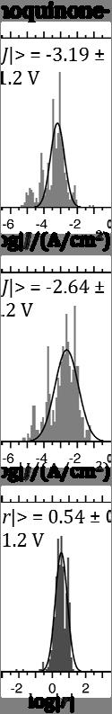
33 Figure 4: Histograms of log r (eq. 2) for junctions containing (A) SAMs of S(CH 2 ) 10 CH 3 and compounds with redox-active terminal groups: (B) naphthoquinone-terminated compound 5, (C) benzoquinone-terminated compound 2, and (D) S(CH 2 ) 11 Fc. Definitions of log r (eq. 2) and R (eq. 3) appear in the text. Solid black curves give the Gaussian functions fitted to each histogram. We note that the SAMs of 2, and 5, whose histograms appear in (B and C), had to be measured at a bias range of ± 1.2 V in order to observe rectification. SAMs of S(CH 2 ) 11 Fc were also stable up to ± 1.2 V and continued to rectify at this bias range (R was roughly unchanged). The dotted line is a guide for the eye at log r = 0 (R = 1). 32


34 Figure 4 33
35 If the Fermi level of the Ag TS electrode in the actual junction were still lower than that of the Ga 2 O 3 /EGaIn electrode, then this difference would increase the positive voltage necessary to bring the LUMO of 2 or 5 into resonance with the Fermi levels of the electrodes (Figure 3). By contrast, this situation would actually reduce the negative voltage necessary to bring the HOMO of Fc into resonance. In any case, we note that, based on a small set of measurements of S(CH 2 ) 11 Fc over the range of V = -1.2 V to 1.2 V, the value of R at ±1.2 V does not differ substantially from the value of R at 1.0 V. We believe, therefore that comparisons between R(1.0 V) for S(CH 2 ) 11 Fc, and R(1.2 V) for 2 and 5, are valid. Figure 4 contains histograms of log r for various compounds, including 2 and 5 (at a bias of ± 1.2 V), as well as S(CH 2 ) 11 Fc and S(CH 2 ) 10 CH 3 (at a bias of ± 1.0 V), for comparison. SAMs with Polar Terminal Groups. We have also formed junctions incorporating SAMs of two compounds with polar, non-redox-active terminal groups: S(CH 2 ) 10 CH 2 OH (11-mercapto-1-undecanol) and S(CH 2 ) 10 COOH (11-thioundecanoic acid). Both compounds are commercially available (Sigma Aldrich). We measured J through these junctions over a range of applied bias from V = -1.0 V to 1.0 V. Histograms of log r, at V = ±1.0 V, for these compounds appear in Figure 5, again with S(CH 2 ) 11 Fc and S(CH 2 ) 10 CH 3 for comparison. The values of R(1.0 V) for S(CH 2 ) 10 CH 2 OH and S(CH 2 ) 10 COOH were 2.5 and 2.4, respectively; these values are statistically distinguishable from R = 1, according to a t-test 42 (see next section). Statistical Significance of Rectification. It is necessary to assess the statistical significance of the values of R in Table 1 by asking two questions: i) is each value of R statistically distinguishable from R = 1? and ii) is each value of R statistically distinct 34
36 Figure 5: Histograms of log r (eq. 2) for junctions containing SAMs of S(CH 2 ) 10 CH 3 (A), two polar terminal groups: S(CH 2 ) 10 CH 2 OH (B) and S(CH 2 ) 10 COOH (C), and S(CH 2 ) 11 Fc (D). Definitions of log r (eq. 2) and R (eq. 3) appear in the text. Solid black curves indicate Gaussian functions fitted to each histogram. The dotted line is a guide for the eye at log r = 0 (R = 1). 35
37 Figure 5 36
38 from the values of R for other compounds (especially the controls that lack molecular asymmetry: S(CH 2 ) 10 CH 3 and S(CH 2 ) 14 CH 3 )? Statistical tests exist to answer these questions, 42 and, since these tests operate on variables with continuous probability distributions (i.e. not R), we applied them to the values of log r for the various compounds. Finding a statistically significant value (or difference between values) of <log r > is, nonetheless, equivalent to finding a statistically significant result for R. A value of R that is statistically significant (i.e. distinguishable from R = 1), in turn, implies an equivalent statistical significance for the sign of R. To answer the first question, we performed t-tests on the distributions of log r for each compound to determine the probability (p) of the null hypothesis: that a distribution was derived from a population with zero mean (i.e. that the value of <log r > was zero). All of these tests rejected the null hypothesis at well above the 95% confidence level (the highest p obtained was , for S(CH 2 ) 6 Fc(CH 2 ) 5 CH 3 ; the rest were many orders of magnitude lower). This result implies that junctions containing every compound in Table 1 can be considered rectifying in the sense of giving rise to statistically significant rectification. We are primarily concerned, however, not with identifying which junctions rectify, but rather identifying which SAMs rectify. For some types of junctions (e.g. those containing alkanethiolates), the observed rectification, although statistically significant, almost certainly arises from something other than the SAM (we discuss several possible origins of the values of R between in the Discussion section). In determining which SAMs rectify, the second question does the value of R for a compound differ from the values of R for other compounds, especially those of controls is much more informative than the first. In order to answer this question, we used a 37
39 Figure 6: Results of a multiple comparison test, performed on the distributions of log r for all ten compounds reported in this paper. For each compound, the vertical dash represents the value of <log r > (Table 1) determined from the Gaussian fit to the histogram of log r, and the horizontal bar represents the confidence interval for the value, calculated by the test. Arrows point to the confidence intervals of the two alkanethiolate controls, and vertical dotted lines indicate the range encompassing both confidence intervals of the alkanethiolate controls. The multiple comparison test is designed such that, if the confidence intervals of any two values of <log r > do not overlap, then the difference between those values is statistically significant. 38
40 Figure 6: 39
41 multiple comparison test, which compares the distributions of log r for all compounds simultaneously, using a procedure similar to a t-test. 42,46,47 The multiple comparison test shows (at the 95% confidence level) whether, for example, the value of R for S(CH 2 ) 11 Fc is statistically distinguishable from the values of R for other compounds. Figure 6 graphically represents the results of the multiple comparison test. Each bar in Figure 6 gives the confidence interval for a particular compound; if the bars of two compounds overlap, then their values of R are not statistically distinguishable from one another. If two bars in Figure 6 do not overlap, however, then the values of R for the corresponding two compounds are statistically different, at the 95% confidence level. According to this test, four compounds S(CH 2 ) 11 Fc 2, S(CH 2 ) 11 Fc, S(CH 2 ) 9 Fc, and compound 5 have values of R that are statistically distinct from those of every other compound, including both alkanethiolate controls (S(CH 2 ) 10 CH 3 and S(CH 2 ) 14 CH 3 ). This test confirms that the compounds terminated by Fc and Fc 2 are, indeed, molecular diodes. While compound 5 also rectifies in a manner that is statistically distinguishable from other compounds, we hesitate to label 5 as a molecular diode, because although it is possible that rectification for compound 5 is molecular in origin, the value of R = 3.5 is too small to be convincing. Hereafter, we will, therefore, use the term molecular diode only in reference to S(CH 2 ) 9 Fc, S(CH 2 ) 11 Fc, and S(CH 2 ) 11 Fc 2. Comparison of Distributions of log J vs. Those of log r. In the Introduction, we discussed the advantages of using rectification, instead of J: rectification is a selfreferencing measurement that is insensitive to factors that vary from junction to junction. Figure 7 compares histograms of log J/(A/cm 2 ) against histograms of log r for three compounds: S(CH 2 ) 11 Fc, 5 (the naphthoquinone-terminated rectifier), and S(CH 2 ) 14 CH 3. 40
42 Figure 7: Comparison of log J/(A/cm 2 ) and log r for three compounds: S(CH 2 ) 11 Fc (left column), 5 (S(CH 2 ) 8 S-naphthoquinone, center column), and S(CH 2 ) 14 CH 3 (right column). Within each column, the top two histograms show log J/(A/cm 2 ) at V and V, respectively (where V is the bias at which R was determined). The bottom histogram (darkened for contrast) in each column shows log r, plotted on the same length of axis (13 orders of magnitude) to enable visual comparison of the distributions of log J/(A/cm 2 ) and log r. All histograms have been fitted with Gaussians (black lines), and the means and standard deviations determined from these Gaussians are shown above each histogram. 41


43 Figure 7 42
The SAM, Not the Electrodes, Dominates Charge Transport in Metal-Monolayer//Ga2O3/ Gallium Indium Eutectic Junctions
 Iowa State University From the SelectedWorks of Martin M. Thuo May, 2012 The SAM, Not the Electrodes, Dominates Charge Transport in Metal-Monolayer//Ga2O3/ Gallium Indium Eutectic Junctions William F.
Supporting Information. The SAM, Not the Electrodes, Dominates Charge Transport in
 Supporting Information The SAM, Not the Electrodes, Dominates Charge Transport in Ag TS -SAM//Ga 2 O 3 /EGaIn Junctions William F. Reus, 1 Martin M. Thuo, 1 Nathan Shapiro 1, Christian A. Nijhuis, 2 and
Supporting Information for. A Molecular Half-Wave Rectifier
 Supporting Information for A Molecular Half-Wave Rectifier Christian A. Nijhuis, 1,* William F. Reus, 2 Adam C. Siegel, 2 and George M. Whitesides 2,* 1 Department of Chemistry, National University of
Molecular electronics. Lecture 2
 Molecular electronics Lecture 2 Molecular electronics approach Electrodes and contacts Basic requirement for molecular electronics: connection of the molecule of interest to the outside world, i.e. electrode
Odd Even Effects in Charge Transport across Self-Assembled Monolayers
 Odd Even Effects in Charge Transport across Self-Assembled Monolayers The Harvard community has made this article openly available. Please share how this access benefits you. Your story matters Citation
Statistical Tools for Analyzing Measurements of Charge Transport
 pubs.acs.org/jpcc Statistical Tools for Analyzing Measurements of Charge Transport William F. Reus, Christian A. Nijhuis, Jabulani R. Barber, Martin M. Thuo, Simon Tricard, and George M. Whitesides*,,
Defining the Value of Injection Current and Effective Electrical Contact Area for EGaIn-Based Molecular Tunneling Junctions
 Defining the Value of Injection Current and Effective Electrical Contact Area for EGaIn-Based Molecular Tunneling Junctions The Harvard community has made this article openly available. Please share how
Comparison of SAM-Based Junctions with Ga 2 O 3 /EGaIn Top Electrodes to Other Large-Area Tunneling Junctions
 pubs.acs.org/jpcc Comparison of SAM-Based Junctions with Ga 2 O 3 /EGaIn Top Electrodes to Other Large-Area Tunneling Junctions Christian A. Nijhuis,, William F. Reus, Jabulani R. Barber, and George M.
Do molecular rectifiers exist?
 Do molecular rectifiers exist? Fatemeh Gholamrezaie June 2006 University of Groningen Faculty of Mathematics and Natural Sciences Materials Science Center plus / Department of Physics 1 Content 1. Introduction
Kinetic equation approach to the problem of rectification in asymmetric molecular structures
 Kinetic equation approach to the problem of rectification in asymmetric molecular structures Kamil Walczak Institute of Physics, Adam Mickiewicz University Umultowska 85, 6-64 Poznań, Poland Transport
Odd-Even Effects in Charge Transport across Self-Assembled Monolayers
 pubs.acs.org/jacs Odd-Even Effects in Charge Transport across Self-Assembled Monolayers Martin M. Thuo, William F. Reus, Christian A. Nijhuis, Jabulani R. Barber, Choongik Kim, Michael D. Schulz, and George
Lecture 9: Metal-semiconductor junctions
 Lecture 9: Metal-semiconductor junctions Contents 1 Introduction 1 2 Metal-metal junction 1 2.1 Thermocouples.......................... 2 3 Schottky junctions 4 3.1 Forward bias............................
Electrical Characterization of Metal Molecule Silicon Junctions
 Electrical Characterization of Metal Molecule Silicon Junctions W. WANG, a T. LEE, a M. KAMDAR, a M.A. REED, a M.P. STEWART, b J.J. HWANG, b AND J.M. TOUR b a Departments of Electrical Engineering, Applied
Semiconductor Polymer
 Semiconductor Polymer Organic Semiconductor for Flexible Electronics Introduction: An organic semiconductor is an organic compound that possesses similar properties to inorganic semiconductors with hole
Supplementary Information. Introducing Ionic and/or Hydrogen Bonds into the SAM//Ga 2 O 3 Top-
 Supplementary Information Introducing Ionic and/or Hydrogen Bonds into the SAM//Ga 2 O 3 Top- Interface of Ag TS /S(CH 2 ) n T//Ga 2 O 3 /EGaIn Junctions Carleen M. Bowers, 1 Kung-Ching Liao, 1, Hyo Jae
Introducing Ionic and/or Hydrogen Bonds into the SAM//Ga 2 O 3 Top-Interface of Ag TS /S(CH 2 ) n T//Ga 2 O 3 /EGaIn Junctions
 n T//Ga 2 O 3 /EGaIn Junctions") Introducing Ionic and/or Hydrogen Bonds into the SAM//Ga 2 O 3 Top-Interface of Ag TS /S(CH 2 ) n T//Ga 2 O 3 /EGaIn Junctions The Harvard community has made this article openly available. Please share
Introducing Ionic and/or Hydrogen Bonds into the SAM//Ga 2 O 3 Top-Interface of Ag TS /S(CH 2 ) n T//Ga 2 O 3 /EGaIn Junctions The Harvard community has made this article openly available. Please share
Self-Assembled Monolayers
 Self-Assembled Monolayers Literature and Further Information Surface Chemistry: www.chem.qmul.ac.uk/surfaces/scc/ www.nottingham.ac.uk/~ppzpjm/amshome.htm venables.asu.edu/grad/lectures.html SAM s: www.ifm.liu.se/applphys/ftir/sams.html
A Single-Level Tunnel Model to Account for Electrical Transport through. Single Molecule- and Self-Assembled Monolayer-based Junctions
 A Single-Level Tunnel Model to Account for Electrical Transport through Single Molecule- and Self-Assembled Monolayer-based Junctions Alvar R. Garrigues 1, Li Yuan 2, Lejia Wang 2, Eduardo R. Mucciolo
Measuring charge transport through molecules
 Measuring charge transport through molecules utline Indirect methods 1. ptical techniques 2. Electrochemical techniques Direct methods 1. Scanning probe techniques 2. In-plane electrodes 3. Break junctions
Direct Measurement of Electron Transfer through a Hydrogen Bond
 Supporting Information Direct Measurement of Electron Transfer through a Hydrogen Bond between Single Molecules Tomoaki Nishino,*, Nobuhiko Hayashi, and Phuc T. Bui Nanoscience and Nanotechnology Research
Review Energy Bands Carrier Density & Mobility Carrier Transport Generation and Recombination
 Review Energy Bands Carrier Density & Mobility Carrier Transport Generation and Recombination The Metal-Semiconductor Junction: Review Energy band diagram of the metal and the semiconductor before (a)
ELEMENTARY BAND THEORY
 ELEMENTARY BAND THEORY PHYSICIST Solid state band Valence band, VB Conduction band, CB Fermi energy, E F Bloch orbital, delocalized n-doping p-doping Band gap, E g Direct band gap Indirect band gap Phonon
Computational Modeling of Molecular Electronics. Chao-Cheng Kaun
 Computational Modeling of Molecular Electronics Chao-Cheng Kaun Research Center for Applied Sciences, Academia Sinica Department of Physics, National Tsing Hua University May 9, 2007 Outline: 1. Introduction
1 Name: Student number: DEPARTMENT OF PHYSICS AND PHYSICAL OCEANOGRAPHY MEMORIAL UNIVERSITY OF NEWFOUNDLAND. Fall :00-11:00
 1 Name: DEPARTMENT OF PHYSICS AND PHYSICAL OCEANOGRAPHY MEMORIAL UNIVERSITY OF NEWFOUNDLAND Final Exam Physics 3000 December 11, 2012 Fall 2012 9:00-11:00 INSTRUCTIONS: 1. Answer all seven (7) questions.
Introducing Ionic and/or Hydrogen Bonds into the SAM//Ga 2 O 3 Top- Interface of Ag TS /S(CH 2 ) n T//Ga 2 O 3 /EGaIn Junctions
 n T//Ga 2 O 3 /EGaIn Junctions") pubs.acs.org/nanolett Introducing Ionic and/or Hydrogen Bonds into the SAM//Ga 2 O 3 Top- Interface of Ag TS /S(CH 2 ) n T//Ga 2 O 3 /EGaIn Junctions Carleen M. Bowers, Kung-Ching Liao, Hyo Jae Yoon, Dmitrij
pubs.acs.org/nanolett Introducing Ionic and/or Hydrogen Bonds into the SAM//Ga 2 O 3 Top- Interface of Ag TS /S(CH 2 ) n T//Ga 2 O 3 /EGaIn Junctions Carleen M. Bowers, Kung-Ching Liao, Hyo Jae Yoon, Dmitrij
Electro - Principles I
 Electro - Principles I Page 10-1 Atomic Theory It is necessary to know what goes on at the atomic level of a semiconductor so the characteristics of the semiconductor can be understood. In many cases a
Electrical rectification by Langmuir Blodgett Monolayers
 Electrical rectification by Langmuir Blodgett Monolayers R M Metzger Presented at the 8th International Conference on Electronic Materials (IUMRS-ICEM 22, Xi an, China, 1 14 June 22) 585 Advanced anomaterials
Surfaces, Interfaces, and Layered Devices
 Surfaces, Interfaces, and Layered Devices Building blocks for nanodevices! W. Pauli: God made solids, but surfaces were the work of Devil. Surfaces and Interfaces 1 Interface between a crystal and vacuum
The experimental work seems to be well carried out and the DFT calculations carefully crafted.
 Reviewers' comments: Reviewer #1 (Remarks to the Author): The manuscript by Maier et al. reports on the on-surface synthesis of 1D and 2D polymers in ultra-high vacuum. A halogenated triphenylamine precursor
Introduction to Semiconductor Devices
 Physics 233 Experiment 48 Introduction to Semiconductor Devices References 1. G.W. Neudeck, The PN Junction Diode, Addison-Wesley MA 1989 2. Background notes (Appendix A) 3. Specification sheet for Diode
Quiz #1 Practice Problem Set
 Name: Student Number: ELEC 3908 Physical Electronics Quiz #1 Practice Problem Set? Minutes January 22, 2016 - No aids except a non-programmable calculator - All questions must be answered - All questions
Chapter 12: Electrical Properties. RA l
 Charge carriers and conduction: Chapter 12: Electrical Properties Charge carriers include all species capable of transporting electrical charge, including electrons, ions, and electron holes. The latter
Supplementary Information. for. Controlled Scalable Synthesis of Uniform, High-Quality Monolayer and Fewlayer
 Supplementary Information for Controlled Scalable Synthesis of Uniform, High-Quality Monolayer and Fewlayer MoS 2 Films Yifei Yu 1, Chun Li 1, Yi Liu 3, Liqin Su 4, Yong Zhang 4, Linyou Cao 1,2 * 1 Department
Supporting Information
 Supporting Information Characterizing the Metal-SAM Interface in Tunneling Junctions Carleen M. Bowers, 1, Kung-Ching Liao, 1, Tomasz Żaba, 2 Dmitrij Rappoport, 1 Mostafa Baghbanzadeh, 1 Benjamin Breiten,
Conjugated Systems, Orbital Symmetry and UV Spectroscopy
 Conjugated Systems, Orbital Symmetry and UV Spectroscopy Introduction There are several possible arrangements for a molecule which contains two double bonds (diene): Isolated: (two or more single bonds
Introduction to Semiconductor Devices
 Physics 233 Experiment 48 Introduction to Semiconductor Devices References 1. G.W. Neudeck, The PN Junction Diode, Addison-Wesley MA 1989 2. Background notes (Appendix A) 3. Specification sheet for Diode
Organic Electronic Devices
 Organic Electronic Devices Week 5: Organic Light-Emitting Devices and Emerging Technologies Lecture 5.5: Course Review and Summary Bryan W. Boudouris Chemical Engineering Purdue University 1 Understanding
Semiconductor Physics fall 2012 problems
 Semiconductor Physics fall 2012 problems 1. An n-type sample of silicon has a uniform density N D = 10 16 atoms cm -3 of arsenic, and a p-type silicon sample has N A = 10 15 atoms cm -3 of boron. For each
Nanoelectronics. Topics
 Nanoelectronics Topics Moore s Law Inorganic nanoelectronic devices Resonant tunneling Quantum dots Single electron transistors Motivation for molecular electronics The review article Overview of Nanoelectronic
Impact of Contact Evolution on the Shelf Life of Organic Solar Cells
 Impact of Contact Evolution on the Shelf Life of Organic Solar Cells By Matthew T. Lloyd, Dana C. Olson, Ping Lu, Erica Fang, Diana L. Moore, Matthew S. White, Matthew O. Reese, David S. Ginley, and Julia
Title. I-V curve? e-e interactions? Conductance? Electrical Transport Through Single Molecules. Vibrations? Devices?
 Electrical Transport Through Single Molecules Harold U. Baranger, Duke University Title with Rui Liu, San-Huang Ke, and Weitao Yang Thanks to S. Getty, M. Fuhrer and L. Sita, U. Maryland Conductance? I-V
Nanoparticle Memories: CMOS, Organic and Hybrid approaches
 Nanoparticle Memories: CMOS, Organic and Hybrid approaches Panagiotis Dimitrakis, Ph.D IMEL/NCSR Demokritos Winter School on Nanoelectronic and Nanophotonics Bilkent University Ankara, Turkey 19-25 January
Charge Transport in Molecular Electronic Junctions: Compression of the Molecular Tunnel Barrier in the Strong. Coupling Regime
 Charge Transport in Molecular Electronic Junctions: Compression of the Molecular Tunnel Barrier in the Strong Coupling Regime Sayed Y. Sayed, Jerry A. Fereiro, Haijun Yan 2, Richard L. McCreery,2, and
Figure 3.1 (p. 141) Figure 3.2 (p. 142)
 Figure 3.2 (p. 142)") Figure 3.1 (p. 141) Allowed electronic-energy-state systems for two isolated materials. States marked with an X are filled; those unmarked are empty. System 1 is a qualitative representation of a metal;
Figure 3.1 (p. 141) Allowed electronic-energy-state systems for two isolated materials. States marked with an X are filled; those unmarked are empty. System 1 is a qualitative representation of a metal;
MSE 310/ECE 340: Electrical Properties of Materials Fall 2014 Department of Materials Science and Engineering Boise State University
 MSE 310/ECE 340: Electrical Properties of Materials Fall 2014 Department of Materials Science and Engineering Boise State University Practice Final Exam 1 Read the questions carefully Label all figures
Electron Transport in Strongly Coupled Molecular Electronic Junctions
 Electron Transport in Strongly Coupled Molecular Electronic Junctions Richard McCreery, Adam Bergren, Sergio Jimenez Bryan Szeto, Jie Ru, Andriy Kovalenko, Stan Stoyanov University of Alberta National
arxiv:cond-mat/ v1 [cond-mat.mes-hall] 19 Dec 2006
![arxiv:cond-mat/ v1 [cond-mat.mes-hall] 19 Dec 2006](/thumbs/91/104898931.jpg "arxiv:cond-mat/ v1 [cond-mat.mes-hall] 19 Dec 2006") arxiv:cond-mat/678v [cond-mat.mes-hall] 9 Dec 6 Abstract Electronic structure of the Au/benzene-,-dithiol/Au transport interface: Effects of chemical bonding U. Schwingenschlögl, C. Schuster Institut für
arxiv:cond-mat/678v [cond-mat.mes-hall] 9 Dec 6 Abstract Electronic structure of the Au/benzene-,-dithiol/Au transport interface: Effects of chemical bonding U. Schwingenschlögl, C. Schuster Institut für
Supporting Information:
 Supporting Information: The Mechanism of Rectification in Tunneling Junctions Based on Molecules with Asymmetric Potential Drops Christian A. Nijhuis, William F. Reus, and George M. Whitesides* Department
Semiconductor Physics and Devices
 The pn Junction 1) Charge carriers crossing the junction. 3) Barrier potential Semiconductor Physics and Devices Chapter 8. The pn Junction Diode 2) Formation of positive and negative ions. 4) Formation
Supporting Information. Charge Transport Across Insulating. Self-Assembled Monolayers: Non-Equilibrium. Approaches and Modeling to Relate Current and
 Supporting Information Charge Transport Across Insulating Self-Assembled Monolayers: Non-Equilibrium Approaches and Modeling to Relate Current and Molecular Structure Fatemeh Mirjani,, Joseph M. Thijssen,
Semiconductors. Semiconductors also can collect and generate photons, so they are important in optoelectronic or photonic applications.
 Semiconductors Semiconducting materials have electrical properties that fall between true conductors, (like metals) which are always highly conducting and insulators (like glass or plastic or common ceramics)
Mat E 272 Lecture 25: Electrical properties of materials
 Mat E 272 Lecture 25: Electrical properties of materials December 6, 2001 Introduction: Calcium and copper are both metals; Ca has a valence of +2 (2 electrons per atom) while Cu has a valence of +1 (1
Today we begin the first technical topic related directly to the course that is: Equilibrium Carrier Concentration.
 Solid State Devices Dr. S. Karmalkar Department of Electronics and Communication Engineering Indian Institute of Technology, Madras Lecture - 3 Equilibrium and Carrier Concentration Today we begin the
Tunneling Spectroscopy of Disordered Two-Dimensional Electron Gas in the Quantum Hall Regime
 Tunneling Spectroscopy of Disordered Two-Dimensional Electron Gas in the Quantum Hall Regime The Harvard community has made this article openly available. Please share how this access benefits you. Your
(a) (b) Supplementary Figure 1. (a) (b) (a) Supplementary Figure 2. (a) (b) (c) (d) (e)
 (b) Supplementary Figure 1. (a) (b) (a) Supplementary Figure 2. (a) (b) (c) (d) (e)") (a) (b) Supplementary Figure 1. (a) An AFM image of the device after the formation of the contact electrodes and the top gate dielectric Al 2 O 3. (b) A line scan performed along the white dashed line
(a) (b) Supplementary Figure 1. (a) An AFM image of the device after the formation of the contact electrodes and the top gate dielectric Al 2 O 3. (b) A line scan performed along the white dashed line
Model of self assembled monolayer based molecular diodes made of ferrocenyl-alkanethiols
 Model of self assembled monolayer based molecular diodes made of ferrocenyl-alkanethiols David Duche, Ujwol Planchoke, Florian-Xuan Dang, Judikaël Le Rouzo, Marc Bescond, Jean-Jacques Simon, Teodor Silviu
Supplementary Figure 1 Experimental setup for crystal growth. Schematic drawing of the experimental setup for C 8 -BTBT crystal growth.
 Supplementary Figure 1 Experimental setup for crystal growth. Schematic drawing of the experimental setup for C 8 -BTBT crystal growth. Supplementary Figure 2 AFM study of the C 8 -BTBT crystal growth
Electron exchange between two electrodes mediated by two electroactive adsorbates
 Electron exchange between two electrodes mediated by two electroactive adsorbates W. Schmickler,* a Maria Anita Rampi, b E. Tran c and G. M. Whitesides c a Abteilung Elektrochemie, University of Ulm, D-89069
Lecture 7: Extrinsic semiconductors - Fermi level
 Lecture 7: Extrinsic semiconductors - Fermi level Contents 1 Dopant materials 1 2 E F in extrinsic semiconductors 5 3 Temperature dependence of carrier concentration 6 3.1 Low temperature regime (T < T
ORGANIC SEMICONDUCTOR 3,4,9,10-Perylenetetracarboxylic dianhydride (PTCDA)
") ORGANIC SEMICONDUCTOR 3,4,9,10-Perylenetetracarboxylic dianhydride (PTCDA) Suvranta Tripathy Department of Physics University of Cincinnati Cincinnati, Ohio 45221 March 8, 2002 Abstract In the last decade
ORGANIC SEMICONDUCTOR 3,4,9,10-Perylenetetracarboxylic dianhydride (PTCDA) Suvranta Tripathy Department of Physics University of Cincinnati Cincinnati, Ohio 45221 March 8, 2002 Abstract In the last decade
Imaging Methods: Scanning Force Microscopy (SFM / AFM)
") Imaging Methods: Scanning Force Microscopy (SFM / AFM) The atomic force microscope (AFM) probes the surface of a sample with a sharp tip, a couple of microns long and often less than 100 Å in diameter.
Imaging Methods: Scanning Force Microscopy (SFM / AFM) The atomic force microscope (AFM) probes the surface of a sample with a sharp tip, a couple of microns long and often less than 100 Å in diameter.
Atomically Resolved Single-Walled Carbon Nanotube Intramolecular Junctions
 Atomically Resolved Single-Walled Carbon Nanotube Intramolecular Junctions The Harvard community has made this article openly available. Please share how this access benefits you. Your story matters Citation
Ch/ChE 140a Problem Set #3 2007/2008 SHOW ALL OF YOUR WORK! (190 Points Total) Due Thursday, February 28 th, 2008
 Due Thursday, February 28 th, 2008") Ch/ChE 140a Problem Set #3 2007/2008 SHOW ALL OF YOUR WORK! (190 Points Total) Due Thursday, February 28 th, 2008 Please read chapter 6 (pp. 175-209) of Advanced Semiconductor Fundamentals by Pierret.
Ch/ChE 140a Problem Set #3 2007/2008 SHOW ALL OF YOUR WORK! (190 Points Total) Due Thursday, February 28 th, 2008 Please read chapter 6 (pp. 175-209) of Advanced Semiconductor Fundamentals by Pierret.
Unit IV Semiconductors Engineering Physics
 Introduction A semiconductor is a material that has a resistivity lies between that of a conductor and an insulator. The conductivity of a semiconductor material can be varied under an external electrical
4.2 Molecular orbitals and atomic orbitals Consider a linear chain of four identical atoms representing a hypothetical molecule.
 4. Molecular orbitals and atomic orbitals Consider a linear chain of four identical atoms representing a hypothetical molecule. Suppose that each atomic wavefunction is 1s wavefunction. This system of
Introduction to Semiconductor Physics. Prof.P. Ravindran, Department of Physics, Central University of Tamil Nadu, India
 Introduction to Semiconductor Physics 1 Prof.P. Ravindran, Department of Physics, Central University of Tamil Nadu, India http://folk.uio.no/ravi/cmp2013 Review of Semiconductor Physics Semiconductor fundamentals
2) Atom manipulation. Xe / Ni(110) Model: Experiment:
 Atom manipulation. Xe / Ni(110) Model: Experiment:") 2) Atom manipulation D. Eigler & E. Schweizer, Nature 344, 524 (1990) Xe / Ni(110) Model: Experiment: G.Meyer, et al. Applied Physics A 68, 125 (1999) First the tip is approached close to the adsorbate
2) Atom manipulation D. Eigler & E. Schweizer, Nature 344, 524 (1990) Xe / Ni(110) Model: Experiment: G.Meyer, et al. Applied Physics A 68, 125 (1999) First the tip is approached close to the adsorbate
UNIVERSITY OF CALIFORNIA College of Engineering Department of Electrical Engineering and Computer Sciences. Fall Exam 1
 UNIVERSITY OF CALIFORNIA College of Engineering Department of Electrical Engineering and Computer Sciences EECS 143 Fall 2008 Exam 1 Professor Ali Javey Answer Key Name: SID: 1337 Closed book. One sheet
1. Binary III-V compounds 2 p From which atoms are the 16 binary III-V compounds formed?...column III B, Al, Ga and In...column V N, P, As and Sb...
 PROBLEMS part B, Semiconductor Materials. 2006 1. Binary III-V compounds 2 p From which atoms are the 16 binary III-V compounds formed?...column III B, Al, Ga and In...column V N, P, As and Sb... 2. Semiconductors
Fundamentals of Semiconductor Physics
 Fall 2007 Fundamentals of Semiconductor Physics 万 歆 Zhejiang Institute of Modern Physics xinwan@zimp.zju.edu.cn http://zimp.zju.edu.cn/~xinwan/ Transistor technology evokes new physics The objective of
Supporting Information
 Supporting Information Monolithically Integrated Flexible Black Phosphorus Complementary Inverter Circuits Yuanda Liu, and Kah-Wee Ang* Department of Electrical and Computer Engineering National University
Engineering 2000 Chapter 8 Semiconductors. ENG2000: R.I. Hornsey Semi: 1
 Engineering 2000 Chapter 8 Semiconductors ENG2000: R.I. Hornsey Semi: 1 Overview We need to know the electrical properties of Si To do this, we must also draw on some of the physical properties and we
arxiv: v1 [physics.comp-ph] 13 Sep 2011
![arxiv: v1 [physics.comp-ph] 13 Sep 2011](/thumbs/89/99260022.jpg "arxiv: v1 [physics.comp-ph] 13 Sep 2011") Theory of electrical rectification in a molecular monolayer C. Krzeminski, C. Delerue, G. Allan, D. Vuillaume Institut d Electronique et de Microélectronique du Nord, arxiv:1109.2695v1 [physics.comp-ph]
Theory of electrical rectification in a molecular monolayer C. Krzeminski, C. Delerue, G. Allan, D. Vuillaume Institut d Electronique et de Microélectronique du Nord, arxiv:1109.2695v1 [physics.comp-ph]
Theory of doping graphene
 H. Pinto, R. Jones School of Physics, University of Exeter, EX4 4QL, Exeter United Kingdom May 25, 2010 Graphene Graphene is made by a single atomic layer of carbon atoms arranged in a honeycomb lattice.
Electron tunneling through alkanedithiol molecules
 Electron tunneling through alkanedithiol molecules R. C. Hoft, J. Liu, M. B. Cortie, and M. J. Ford, Institute for Nanoscale Technology, University of Technology Sydney, P. O. Box 123, Broadway, NSW 2007,
e - Galvanic Cell 1. Voltage Sources 1.1 Polymer Electrolyte Membrane (PEM) Fuel Cell
 Fuel Cell") Galvanic cells convert different forms of energy (chemical fuel, sunlight, mechanical pressure, etc.) into electrical energy and heat. In this lecture, we are interested in some examples of galvanic cells.
Galvanic cells convert different forms of energy (chemical fuel, sunlight, mechanical pressure, etc.) into electrical energy and heat. In this lecture, we are interested in some examples of galvanic cells.
Lecture 2 and 3: Review of forces (ctd.) and elementary statistical mechanics. Contributions to protein stability
 and elementary statistical mechanics. Contributions to protein stability") Lecture 2 and 3: Review of forces (ctd.) and elementary statistical mechanics. Contributions to protein stability Part I. Review of forces Covalent bonds Non-covalent Interactions: Van der Waals Interactions
Lecture 2 and 3: Review of forces (ctd.) and elementary statistical mechanics. Contributions to protein stability Part I. Review of forces Covalent bonds Non-covalent Interactions: Van der Waals Interactions
Core Level Spectroscopies
 Core Level Spectroscopies Spectroscopies involving core levels are element-sensitive, and that makes them very useful for understanding chemical bonding, as well as for the study of complex materials.
FREQUENTLY ASKED QUESTIONS February 21, 2017
 FREQUENTLY ASKED QUESTIONS February 21, 2017 Content Questions How do you place a single arsenic atom with the ratio 1 in 100 million? Sounds difficult to get evenly spread throughout. Yes, techniques
Supporting Information
 Supporting Information Oh et al. 10.1073/pnas.0811923106 SI Text Hysteresis of BPE-PTCDI MW-TFTs. Fig. S9 represents bidirectional transfer plots at V DS 100VinN 2 atmosphere for transistors constructed
Schottky Rectifiers Zheng Yang (ERF 3017,
 ECE442 Power Semiconductor Devices and Integrated Circuits Schottky Rectifiers Zheng Yang (ERF 3017, email: yangzhen@uic.edu) Power Schottky Rectifier Structure 2 Metal-Semiconductor Contact The work function
Chapter 4: Bonding in Solids and Electronic Properties. Free electron theory
 Chapter 4: Bonding in Solids and Electronic Properties Free electron theory Consider free electrons in a metal an electron gas. regards a metal as a box in which electrons are free to move. assumes nuclei
Module-6: Schottky barrier capacitance-impurity concentration
 6.1 Introduction: Module-6: Schottky barrier capacitance-impurity concentration The electric current flowing across a metal semiconductor interface is generally non-linear with respect to the applied bias
Supplementary Figure 1: Power dependence of hot-electrons reduction of 4-NTP to 4-ATP. a) SERS spectra of the hot-electron reduction reaction using
 SERS spectra of the hot-electron reduction reaction using") Supplementary Figure 1: Power dependence of hot-electrons reduction of 4-NTP to 4-ATP. a) SERS spectra of the hot-electron reduction reaction using 633 nm laser excitation at different powers and b) the
Supplementary Figure 1: Power dependence of hot-electrons reduction of 4-NTP to 4-ATP. a) SERS spectra of the hot-electron reduction reaction using 633 nm laser excitation at different powers and b) the
Chem 481 Lecture Material 3/20/09
 Chem 481 Lecture Material 3/20/09 Radiation Detection and Measurement Semiconductor Detectors The electrons in a sample of silicon are each bound to specific silicon atoms (occupy the valence band). If
Molecular Rectification in a Metal-Insulator-Metal Junction Based on Self-Assembled Monolayers
 Published on Web 09/10/2002 Molecular Rectification in a Metal-Insulator-Metal Junction Based on Self-Assembled Monolayers Michael L. Chabinyc, Xiaoxi Chen, R. Erik Holmlin, Heiko Jacobs, Hjalti Skulason,
Title of file for HTML: Supplementary Information Description: Supplementary Figures and Supplementary References
 Title of file for HTML: Supplementary Information Description: Supplementary Figures and Supplementary References Supplementary Figure 1. SEM images of perovskite single-crystal patterned thin film with
Chapter 5. Semiconductor Laser
 Chapter 5 Semiconductor Laser 5.0 Introduction Laser is an acronym for light amplification by stimulated emission of radiation. Albert Einstein in 1917 showed that the process of stimulated emission must
Semiconductor Physics Problems 2015
 Semiconductor Physics Problems 2015 Page and figure numbers refer to Semiconductor Devices Physics and Technology, 3rd edition, by SM Sze and M-K Lee 1. The purest semiconductor crystals it is possible
Metal Semiconductor Contacts
 Metal Semiconductor Contacts The investigation of rectification in metal-semiconductor contacts was first described by Braun [33-35], who discovered in 1874 the asymmetric nature of electrical conduction
V + XOR AND. Architectures HS for molecular electronic computers: molecular electronic diodes MITRE. James C. Ellenbogen J.
 SH XOR H C 2 CH 2 H 2 C V N C CH 2 Architectures HS for molecular electronic computers: 1. Logic structures H 3 C O and H 2 an C adder designed from A B HS H 3 C O CH 2 C N molecular electronic diodes
ITT Technical Institute ET215 Devices I Unit 1
 ITT Technical Institute ET215 Devices I Unit 1 Chapter 1 Chapter 2, Sections 2.1-2.4 Chapter 1 Basic Concepts of Analog Circuits Recall ET115 & ET145 Ohms Law I = V/R If voltage across a resistor increases
PCCP PERSPECTIVE. A critical perspective on molecular electronic junctions: there is plenty of room in the middle. 1. Introduction
 PERSPECTIVE Cite this: Phys. Chem. Chem. Phys., 2013, 15, 1065 A critical perspective on molecular electronic junctions: there is plenty of room in the middle Richard L. McCreery,* ab Haijun Yan a and
LS1a Fall 2014 Problem Set #2 Due Monday 10/6 at 6 pm in the drop boxes on the Science Center 2 nd Floor
 LS1a Fall 2014 Problem Set #2 Due Monday 10/6 at 6 pm in the drop boxes on the Science Center 2 nd Floor Note: Adequate space is given for each answer. Questions that require a brief explanation should
Chapter 25: The Chemistry of Life: Organic and Biological Chemistry
 Chemistry: The Central Science Chapter 25: The Chemistry of Life: Organic and Biological Chemistry The study of carbon compounds constitutes a separate branch of chemistry known as organic chemistry The
Semiconductor Optoelectronics Prof. M. R. Shenoy Department of Physics Indian Institute of Technology, Delhi. Lecture - 13 Band gap Engineering
 Semiconductor Optoelectronics Prof. M. R. Shenoy Department of Physics Indian Institute of Technology, Delhi Lecture - 13 Band gap Engineering (Refer Slide Time: 00:38) Let us continue with the lectures,
Molecular Geometry: VSEPR model stand for valence-shell electron-pair repulsion and predicts the 3D shape of molecules that are formed in bonding.
 Molecular Geometry: VSEPR model stand for valence-shell electron-pair repulsion and predicts the 3D shape of molecules that are formed in bonding. Sigma and Pi Bonds: All single bonds are sigma(σ), that
UNIVERSITY OF CALIFORNIA College of Engineering Department of Electrical Engineering and Computer Sciences. EECS 130 Professor Ali Javey Fall 2006
 UNIVERSITY OF CALIFORNIA College of Engineering Department of Electrical Engineering and Computer Sciences EECS 130 Professor Ali Javey Fall 2006 Midterm 2 Name: SID: Closed book. Two sheets of notes are
Identification and Quantification of Impurities Critical to the Performance of Nitride Semiconductor Devices
 Identification and Quantification of Impurities Critical to the Performance of Nitride Semiconductor Devices R. Torres*, J. Vininski, C. Wyse, Advanced Technology Center, Matheson-Trigas, Inc., Longmont,
Supporting Information: Molecular Interfaces for Plasmonic Hot Electron. Photovoltaics
 Electronic Supplementary Material (ESI) for Nanoscale. This journal is The Royal Society of Chemistry 2015 Supporting Information: Molecular Interfaces for Plasmonic Hot Electron Photovoltaics F. Pelayo