UNIVERSITY OF NAPLES FEDERICO II
|
|
|
- Kenneth O’Neal’
- 5 years ago
- Views:
Transcription

1 UNIVERSITY OF NAPLES FEDERICO II SCHOOL OF DOCTORATE IN CHEMICAL SCIENCES Nanostructured polymeric materials for morphology control on nanometer scale and nanotechnology applications by Claudia Diletto Tutors: Prof. Claudio De Rosa Prof. Auriemma Finizia Opponent: Prof. Vincenzo Pavone
2 Abstract Symmetric and asymmetric poly(styrene-b-methylmethacrylate) (PS-b-PMMA) diblock copolymers (BCPs) were used as template for the incorporation of inorganic nanoparticles and/or organic molecules. Innovative nanocomposites based on a nanostructured block copolymer matrix whose lamellar and cylindrical nanodomains are selectively loaded with inorganic nanoparticles and/or organic molecules, were prepared. This study was aimed to the preparation of neat BCP and nanocomposites thin films by spin-coating and/or drop casting. Techniques as application of external electric fields and solvent annealing were developed in order to improve the morphological order of the neat copolymer and of the nanocomposites. These materials were used as substrates for surface-enhanced Raman spectroscopy (SERS) and as active layers for solar cells.
3 Table of Contents 1 Nanostructure fabrication using Block Copolymers Introduction Block copolymer architecture and general principles Methodologies to align and orient on long-range scale the morphologies of block copolymers Thermal Annealing Use of template Specific surface interactions Application of external fields Applications of BCPs Nanocomposites Description of the thesis work 27 Bibliography of Chapter I 29 2 Materials and methods - Experimental part Analyzed samples Thin film deposition technique: spin-coating Thermal and structural analysis Thermal analysis Wide angle X-ray scattering (WAXS) Morphological analysis 42
4 2.4.1 Transmission electron microscopy (TEM) Atomic Force Microscopy (AFM) Scanning electron microscopy (SEM) Profilometry UV-VIS Measurements I-V Measurements Raman Spectroscopy and Surface-Enhanced Raman Spectroscopy (SERS) 49 Bibliography of Chapter II 54 3 Ordering of nanostructured BCP based hybrid thin films over large area Characterization of PS-b-PMMA block copolymer with lamellar Morphology Thermal and structural analysis Morphological analysis of the neat PS-b-PMMA A novel approach to obtain ordered periodic structures based on PS-b-PMMA and gold nanoparticles External Electric Fields to induce long range order to PS-b-PMMA nanostructures Nanoparticles 70
5 3.2.3 Gold Nanoparticles Nanocomposites from block copolymer ordered lamellar nanostructures and selective gold deposition Characterization of nanocomposites based on PS-b-PMMA block copolymer with cylindrical morphology and gold nanoparticles obtained by chemical synthesis Thermal analysis of neat PS-b-PMMA Morphological analysis of the neat PS-b-PMMA Synthesis of Thiol-derivatised Gold Nanoparticles Thermogravimetric analysis of nanoparticles (NT-AuNPs) UV-Vis spectra measurements of nanoparticles (NT-AuNPs) TEM analysis of nanoparticles (NT-AuNPs) Nanocomposites based on PS-b-PMMA and NT-AuNPs with long range order Nanocomposites from block copolymer cylindrical nanostructures and selective gold deposition Characterization of nanocomposites based on PS-b-PMMA block copolymer with lamellar morphology and zinc oxide nanoparticles obtained by chemical synthesis ZnO NPs: crystal structure Applications of ZnO NPs ZnO Nanocrystals by a Non-hydrolytic Route Optical end morphological characterization of ZnO NPs 100
6 3.5.5 Nanocomposites based on lamellar PS-b-PMMA and ZnO NPs 101 Bibliography of Chapter III BCP/AuNPs hybrid and BCP/organic molecules nanocomposites for optoelectronic applications Nanocomposites based on PS-b-PMMA lamellar nanostructures and AuNPs as SERS substrates Nanocomposites based on PS-b-PMMA lamellar nanostructures and organic molecules as active layers in photovoltaic cells Zinc Oxide Nanoparticles as p layers within inorganic solar cells 134 Bibliography of Chapter IV 138 Conclusions 144
7 7
8 CHAPTER I Nanostructure fabrication using Block Copolymers 1.1 Introduction Nanotechnology has found an incredible resonance and a vast number of applications in many areas during the past two decades. The resulting deep paradigm shift has opened up new horizons in materials science, and has led to exciting new developments. Fundamentally, nanotechnology is dependent on the existence or the supply of new nanomaterials that form the prerequisite for any further progress in this new and interdisciplinary area of science and technology. Evidently, nanomaterials feature specific properties that are characteristic of this class of materials, and which are based on surface and quantum effects. Clearly, the control of composition, size, shape, and morphology of nanomaterials is an essential cornerstone for the development and application of nanomaterials and nanoscale devices. The complex functions of nanomaterials in devices and systems require further advancement in the preparation and modification of nanomaterials. Such advanced nanomaterials have attracted tremendous interest during recent years, and will form the basis for further progress in this area. At the present time, block-copolymer-based materials have attracted much attention in view of their potential applications, since the self-assembly capacity of this kind of materials with nanoscale periodicity allows creating of nanopatterned structures. Several studies have reported the use of block-copolymers (BCPs) as templates for the synthesis of nanostructured materials because of their ability to control both the size and the spatial organization by varying their composition and molecular weight. The present research activity fits in the field of organic electronics, a multidisciplinary sector of modern materials science that is focused on the study of new materials for electronics based on organic compounds or, more generally, based on carbon rather than on silicon as traditional electronics. The development of organic electronics in the last years has been basically entrusted to the study of conductive polymers or polymer based nanocomposites, in which metal or magnetic nanoparticles are dispersed in polymeric matrix constituted by amorphous homopolymers. Metal, semiconductive and magnetic nanoparticles have the potential to become the fundamental building blocks in microelectronic, optical and memory devices, due to their unique properties that bridge 8
9 between the molecular and the macroscopic worlds. However, utilization of nanoparticles is hindered by our currently limited ability to organize them in periodic arrays of predefined structures. An innovative and promising approach that we used in this project is the utilization of block copolymers, rather than homopolymers, as a matrix for the dispersion of nanoparticles, in which the nanostructured matrix act as directing media that guides the ordered organization of nanoparticles in a mutual self-assembly process, allowing for a long-range order in the positioning of nanofillers. BCPs form, indeed, spontaneously nanostructures, thanks to self-assembly phenomena generated by phase separation of incompatible polymeric blocks. The main research activity of this PhD thesis was addressed to develop innovative systems where a nanostructured block copolymer is selectively loaded with organic molecules and inorganic nanoparticles. 1.2 Block copolymer architecture and general principles In the last decades block copolymers have generated a huge interest in the field of nanotechnologies 1-18 thanks to their capability to form by self-assembly structures with periodicity at nanometric scale. In BCPs macromolecules of two or more different homopolymers are chemically linked to form complex macromolecules with linear architecture (di-, tri-, multiblock copolymers) or not linear (mixed arm, starblock, o graft copolymers) (Figure 1.1). Figure 1.1. Linear or not linear architectures of block copolymers. If different polymeric blocks are chemically incompatible, phase separation with spontaneous segregation of different macromolecules in diverse microdomains (Figure 1.2) occurs. The formed microdomains are arranged according to regular disposition giving rise to the formation of periodical structures. 9

10 The thermodynamics of polymer mixing plays a large role in the self - assembly of BCPs. 19 In typical binary polymer mixtures, it is entropically unfavorable for two dissimilar homopolymers to mix homogeneously, as both components feel repulsive forces that result in the formation of large macrophases of each component in the mixture, akin to the mixing of oil and water. In diblock copolymers, however, the two component polymer blocks are chemically attached with a covalent bond. Figure 1.2. Self-assembly scheme in BCPs due to phase separation. Here, the covalent bond acts as an elastic restoring force that limits the phase separation to mesoscopic length scales, thus resulting in microphase separated structures. The size of these phases, which are also known as microdomains, scale directly as the two - thirds power of the copolymer molecular weight. 20 The specific shape of the microdomains relies on a number of factors that control how each of the blocks interacts with each other. In the simplest argument, if there are equal amounts of each polymer, the microdomains will form into distinct layers with planar interfaces. However, if there is more of one block than the other, then curved interfaces will result. This curvature minimizes the repulsive interfacial contact between the A and B block, which also minimizes the free energy of the system. The bend that forms can be characterized by the curvature radius, R, as shown in Figure 1.3. Therefore, the equilibrium morphology of the BCP can usually be predicted based on differential geometry. Other, more complicated, self-consistent mean field theoretical treatments can be used to calculate the equilibrium morphology of the BCP. These theories sum the free energy contributions between (i) the repulsive polymer- polymer interactions versus (ii) the elastic restoring force energy for a particular microphase structure. The microphase structure with the lowest free energy sum will be the final equilibrium morphology. 10
 to minimize interfacial contact between the blocks and cause decrease of the curvature radius; (b)")

11 Figure 1.3. (a) Equal volume fractions of A and B blocks form layered structures called lamellae with curvature radius approaching infinity. Unequal volume fractions of A and B cause a curvature at the intermaterial dividing surface (IMDS) to minimize interfacial contact between the blocks and cause decrease of the curvature radius; (b) Schematic representing the application of this model in a sphere forming (PS-b-PMMA) block copolymer system. Figure 1.4. Phase diagram for linear AB diblock copolymers, comparing theory and experiment. (a) Self - consistent mean field theory predicts four equilibrium morphologies: spherical (S), cylindrical (C), gyroid (G), and lamellar (L), depending on the composition f and combination parameter χ N. Here, χ is the Flory-Huggins interaction parameter (proportional to the heat of mixing A and B segments) and N is the degree of polymerization (number of monomers of all types per macromolecule); (b) Experimental phase portrait for poly(isoprene bloc -styrene) diblock copolymers. Note the resemblance to the theoretical diagram. One difference is the observed perforated lamellae (PL) phase, which is actually metastable; (c) A representation of the equilibrium microdomain structures as f A is increased for fixed χn. 11

12 These theoretical equilibrium morphologies can be mapped out on a phase diagram, as shown in Figure 1.4. A typical BCP phase diagram plots the product χ N on the ordinate versus the volume ratio, f A, on the independent axis. χ is known as the Flory-Huggins interaction parameter, which quantifies the relative incompatibility between the polymer blocks, and is inversely related to the temperature of the system. N is called the degree of polymerization, which is the total number of monomers per macromolecule. The volume fraction is represented by f A = N A /N, where N A is the number of A monomers per molecule. For very low concentrations of A monomer, no phase separation will occur and the two polymers will mix homogeneously. However, at slightly higher compositions, where f A <<f B, the A blocks form spherical microdomains in a matrix of B. The microdomains arrange on a bodycentered cubic (BCC) lattice. Increasing the volume fraction to fa<fb leads to an increase in the connectivity of the microdomains, triggering the spheres to coalesce into cylinders that arrange on a hexagonal lattice. A roughly equal amount of both A and B blocks (f A f B ) will result in the formation of alternating layered sheets, or lamellae, of the A and B blocks. Any further increase in f A (f A >f B ), will cause the phases to invert, which means that the B block forms the microdomains in the matrix of A. A few of these morphologies, the ones most frequently used for nanofabrication, are illustrated schematically in figure 1.5. Figure 1.5. Sketches of equilibrium morphologies from BCP self-assembly, among the most frequently used for nanofabrication. For diblock copolymers in bulk: body-center cubic-packed spheres (1), hexagonally ordered cylinders (2), lamellae (3). For triblock copolymers: lamellae (4), hexagonally coaxial cylinders (5), Spheres between lamellae (6). For amphiphilic BCPs in solution: spherical micelles (7), and cylindrical micelles (8). Periodicities, or micellar dimension, are in the range nm. 12
13 Thus, by tailoring the relative amount of A, the chemist can control the connectivity and dimensionality of the global BCP structure: spheres essentially represent zero-dimensional points in a matrix; cylinders represent one-dimensional lines; and lamellae represent two - dimensional sheets. Additionally, narrow regions of f A exist in between the cylindrical and lamellar phase space where the two morphologies interpenetrate each other to form three- dimensional (3-D) gyroid 21,22 network structures. Some reports of these morphologies have been published, and efforts have been put forth to take advantage of the added dimensionality with new application. 23,24 From this point of view block copolymers represent a class of amorphous materials able to organize themselves in similar structures of those of crystalline materials, with the strong difference that the dimensions of the repetitive units and the periodicity are not of the order of angstrom, as in the crystals, but of nanometers. The dimensions of the microdomains where polymeric blocks are segregated (spheres, cylinders and lamellae) and also the periodicity of the microstructure depend from the length of the blocks and consequently form the molecular masses of the blocks. This fact permits tuning the dimensions of microdomains and the periodicity in a wide range, from tens to hundreds nanometers, adjusting the molecular masses of the blocks. The molecular architectures that could be developed by the classical anionic polymerization procedures vary from the linear diblock 25, to the linear tri- or multi-block 25, to more complex geometries as the star nanostructure 26. All these geometries permit to create patterns on the thin films surface hardly practicable with the traditional lithography techniques. 1.3 Methodologies to align and orient on long-range scale the morphologies of block copolymers Except for some specific instances, such as direct use as photonic crystals or in the case of amphiphilic BC for drug and genetic delivery, applications of BCs require the preparation of thin films with thicknesses ranging from a few tens of nanometers (in some cases down to thicknesses of less than the corresponding equilibrium period of the BC) to several micrometers. Films with low surface roughness may be produced by spin coating or dip coating from relatively dilute solutions, that is, approximately 1-5% by weight, onto solid substrates with uniform flatness. The thickness and the uniformity of the film surface mainly depend on the concentration of the solution, the volatility of the solvent, and the specific instrumental speed that is, the spin speed or withdrawal speed, respectively. During dip coating processes, and also for films prepared from direct casting, the solvent may evaporate slowly, thus allowing a stable organization of macromolecules close to thermodynamic equilibrium. In contrast, in the case of spun cast films the solvent is driven off so 13

14 quickly that non equilibrium structures could be observed. In thin films, the self assembled BC morphologies are influenced not only by molecular weights, polydispersity and composition, but also by other variables such as the selectivity of the solvent for one block, surface interfacial interactions, and the interplay between structure periodicity and film thickness, which can cause significant deviations from the predicted phases in the bulk state. Independently of the casting techniques, even for a film prepared taking all necessary precautions, it is not possible to obtain a perfectly ordered morphology over a large area. First, when a BCP thin film is created, the microdomains will often seem disordered, appearing in randomly oriented grains along the sample surface. Long range ordering of the BCP nanodomains is often necessary for a few of the possible applications of BCP, such as in the creation of addressable, high-density information storage media. Second, the nanodomains tend to arrange parallel to the sample surface due to preferred interfacial interactions between one of the blocks and the substrate. However, in order to be lithographically useful as etch masks that are able to transfer patterns into a wafer, nanodomains such as lamellae and cylinders must be arranged perpendicularly so that they are physically and continuously connected from the polymer/air interface through to the substrate, as shown in the plan-view and cross-sectional scanning electron microscopy (SEM) images shown in Figure 1.6. Figure 1.6. Field effect scanning electron microscopy images obtained from a thin film of PS-b-PMMA after removal of the PMMA block. (a) Top view of the film; (b) A cross sectional view. Third, the thickness of the BCP must be carefully controlled. Many research groups have achieved success in controlling the orientation of the self-assembled structures through special processing strategies 27 ; these include techniques such as thermal annealing 28, electric fields 29,30, mechanical shear 31-33, exposure to solvent vapor, 34,35 physical confinement, 36 neutral surfaces 37,38 chemically nanopatterned surfaces or a combination of any of the above. 42 As discussed below, the optimization process can be carried out using different strategies. 14
 of the constituent blocks, preferably in an inert atmosphere or under vacuum, for a specific time.")
15 1.3.1 Thermal Annealing Thermal annealing is the simplest option and the most commonly used method. This consists of controlled heating at a temperature above the glass transition temperature (T g ) of the constituent blocks, preferably in an inert atmosphere or under vacuum, for a specific time. For polymers with high molecular weights and complex architectures, the high degree of chain entanglements and the difficult diffusion of one polymer block through the domains of the other blocks pose large kinetic barriers to equilibrium. In such cases, and for partially crystalline BCs with high melting temperatures, the annealing window for the relevant conditions of temperature and time that are theoretically necessary and those of the order disorder transition or polymer decomposition, may be insufficient to reach equilibrium Use of template The combination of top-down strategies to fabricate patterns that direct the bottom-up organization of organic or inorganic building blocks is an approach often used in the micrometer and, to a minor extent, in the nanometer regime. Also, in the case of BCPs, the long-range order and orientation may be induced if self-assembly is forced to occur into/onto a guide, either topographically or chemically patterned, or in other 2D- or 3D-confinements. An innovative fabrication strategy that employs advanced lithographic techniques has been developed, by Nealey and coworkers, to produce perfect periodic domain ordering. 40,41 As reported in Figure 1.7, in the first fundamental step of this procedure a self-assembled monolayer (SAM) is precisely patterned throughout the photoresist using extreme ultraviolet interferometric lithography. 43,44 Figure 1.7. Schematic representation of the fabrication process of chemically nanopatterned surfaces that template the self assembly of symmetric PS-b-PMMA. (a) A self assembled monolayer of phenylethyltrichlorosilane is deposited on a silicon wafer; (b) A photoresist is then spin coated and patterned with alternating lines and spaces by ultraviolet interferometric lithography (c); (d) The topographic pattern is converted into a chemical pattern by irradiation with soft X-rays in the presence of oxygen; (e) After the photoresist removal, a toluene solution of PS-b-PMMA is spin coated 15 onto the patterned SAM (f). (g) Thermal annealing facilitates.
16 Following the conversion of the topographic pattern to a chemical pattern and the photoresist removal, a symmetric PS-b-PMMA is spin-coated onto the chemically patterned substrate and, as the modified regions present polar groups that preferentially wet the PMMA block, the selfassembly results in lamellae oriented perpendicular to the substrate Specific surface interactions The control of the orientation of the microdomains in the microstructure of the BCPs can be obtained through a bias field induced by surface interactions. Different types of interactions can be established depending on the nature of the surface and of the BCP. 27 The simplest interaction of a BCP film deposited on a substrate is the preferential wetting of one block at an interface to minimize interfacial and surface energies. As a consequence, a parallel orientation of microdomains, lamellae and cylinders is often induced at the interface and this orientation tends to propagate throughout the entire film. 13,45-56 The microstructure can be altered by variation of the film thickness on the substrate and preferential interactions of blocks with the substrate. 54,55 Symmetric boundary conditions are established when one of the blocks preferentially interacts with both the substrate and the air surface, 50 while asymmetric conditions pertain when one block is preferentially wetted by the substrate and the other block by the superstrate. The control of orientation of the microdomains can also be achieved by confining a BC between two surfaces; that is, adding a superstrate to a BC film supported on a substrate Strong or weak interactions of BCs with the surfaces can be created by coating the surface walls with a homopolymer or a random copolymer, respectively, containing the same chemical species as the confined BC. 59 In the case of a neutral surface, for example, by using a random copolymer, the lamellar microdomains rearrange themselves so that the direction of periodicity is parallel to the substrate. 59,61-63 Moreover, decreasing the confined film thickness that is, creating a large incompatibility strain of the natural domain period of the BC and the film thickness induces a heterogeneous in - plane structure where both parallel and perpendicular lamellae are located near the confining substrate. 60 Various theoretical studies have predicted the structural behavior of BC thin films in a confined geometry and are basically consistent with experimental results. Epitaxy is defined as the oriented growth of a crystal on the surface of a crystal of another substance (the substrate). The growth of the crystals occurs in one or more strictly defined 16
17 crystallographic orientations defined by the crystal lattice of the crystalline substrate The resulting mutual orientation is due to a 2D or, less frequently, a 1D-structural analogy, with the lattice matching in the plane of contact of the two species. 74 The term epitaxy, literally meaning on surface arrangement, was introduced in the early theory of organized crystal growth based on structural matching. Discrepancy between atomic or molecular spacings is measured by the quantity 100(d d0)/d0, where d and d0 are the lattice periodicities of the adsorbed phase and the substrate, respectively. In general 10 15% discrepancies are considered as an upper limit for epitaxy to occur in polymers. 76 Inorganic substrates were first used for the epitaxial crystallization of polymers. 77,78 Successive studies have demonstrated the epitaxial crystallizations of polyethylene (PE) and linear polyesters onto crystals of organic substrates, such as condensed aromatic hydrocarbons (naphthalene, anthracene, phenanthrene, etc.), linear polyphenyls and aromatic carboxylic acids. 79,80 In the case of PE, a unique orientation of the crystals grown on all the substrates is observed, with different contact planes depending on the substrate. 81 An example of an epitaxial relationship between PE crystals and an organic substrate is shown in Figure 1.8, with the substrate constituted by a crystal of benzoic acid 82 (monoclinic structure with a = 5.52 Å, b = 5.14 Å, c = 21.9 Å and β = 97, with a melting temperature of 123 C). Figure 1.8. PE lamella oriented edge-on on the (001) face of a BA crystal substrate after epitaxial crystallization. The (100) plane of PE is in contact with the (001) plane of BA, and b- and c-axes of PE are parallel to b and a-axes of BA, respectively. 17
18 A clear match between the PE interchain distance (the b-axis of PE equal to 4.95 Å) and the b-axis periodicity of benzoic acid crystal (5.14 Å), and between the c-axis periodicity of PE (2.5 Å) and the a-axis of benzoic acid crystal (5.52 Å), produces the crystallization of PE onto preformed crystals of benzoic acid with lamellae standing edge-on, that is, normal to the surface of benzoic acid crystal. The PE polymer chains lie flat on the substrate surface with their chain axis parallel to the substrate surface and parallel to the a-axis of benzoic acid crystal, and the b-axis of PE parallel to the b-axis of BA crystal. 82 The (100) plane of PE is in contact with the (001) exposed face of benzoic acid. Epitaxy carries out an industrial relevance because works as basis of the nucleating activity for many nucleating and clarifying agents. It is also an ideal tool to design thin films with long-range order as for optoelectronic devices. 83 Directional solidification. In many cases substrates can be melted and act as solvents for the polymer but only in their melt state. In this case, a small quantity of the substrate is melt together with the polymeric film between two glass slides (preferably two thin ones to minimize the thermal inertia during quenching). During the quenching, substrate crystallizes at first, then the polymer crystallizes on the substrate surface. This process is observed frequently when the polymer and the substrate have similar melting temperature, and form an eutectic. 84 The possible epitaxial crystallization of the polymer brings a further specificity to the entire process. 83 Graphoepitaxy is a process whereby an artificial surface topography of a crystalline or amorphous substrate influences and controls the orientation of the crystal growth in thin films Graphoepitaxy has been used, often in combination with epitaxy, to obtain high orientation of polymeric crystals onto substrates constituted by films of other polymers Application of external fields Since the first macroscopic alignment of cylindrical domains of an industrial tri-block copolymer (a PS-b-PB-b-PS, Kraton 102, with PB = polybutadiene) by extrusion carried out by the Keller group in the early 1970s, 94,95 several mechanical flow fields have been proposed to control BCP alignment even though the success of these attempts was limited. In the 1990s research interests returned massively toward alignment strategies of BCP nanostructures by identification of weak external fields due the increased availability of BCPs with different architectures and chemical compositions. Particularly in recent years, most investigations moved from bulk materials 18
19 to thin films, due to their nanotechnological potential, with a special focus on the use of electric fields. The principal techniques that have been employed to control the BCP long-range order are: Mechanical flow fields as extrusion, 94,95 compression, flows involving oscillatory shear and other steady shear techniques, up to techniques that combine different flow fields have been successfully applied to induce alignment in BCPs. Magnetic Fields. A further alignment approach is available for materials that exhibit anisotropic susceptibility due to an anisotropic molecular structure. Magnetic field induced orientation has been achieved for liquid crystalline diblock copolymers with a dielectric diamagnetic isotropy, possibly through the magnetic alignment of LC mesogens 120,121 and also for BCPs with a crystallizable block through an accurate control of the crystallization process. 122 Magnetic fields also offer the ability to apply very high fields without the risks of electric fields, associated with the danger and limit of electric breakdown. The observation of lamellar and cylindrical microdomains in thin films perpendicular to the surface as a result of solvent evaporation was first reported by Turturro and coworkers 123 and then investigated in more detail by Kim and Libera for a similar triblock copolymer. 124,125 On the basis of these and other studies on either spun-cast or solution-cast films from solutions in a good solvent for all the blocks, a reasonable mechanism of orientation was proposed (Figure 1.9). At the beginning of film deposition the Tg of the swollen film is still well below room temperature, thus allowing free chain mobility. With the decrease in the solvent concentration, the BCP undergoes a transition from the disordered to the ordered state and, as the diffusion of the solvent produces a gradient of concentration along the thickness of the thin film, the ordering front rapidly propagates from the air surface to the substrate. The consequent decrease of Tg below room temperature, for at least one block, locks in the structures, which, due to the high directionality of the solvent gradient, are highly oriented normal to the surface. This behavior has been reported so far for films with thickness less than one-half micron, as for instance in the case of PS-PB systems, 123,42 polystyrene-block-poly(ethylene oxide) (PS-b-PEO) 126,127 polystyrene-bpolyferrocenyldimethylsilane (PS-b-PFS). 128 However this mechanism holds to any BCPs having the Tg of one block above room temperature. 19

20 Figure 1.9. Schematic of the solvent evaporation in a diblock copolymer thin film. 42 The diffusion produces a gradient in the concentration of the solvent, [S], as a function of depth, d, which induces an ordering front from the film surface to the substrate. Static electric fields have been widely used in copolymer melts to macroscopically orient lamellar or cylindrical morphologies Microdomains parallel to the substrate can be obtained using an in-plane field. A uniaxial orientation along the field and perpendicular to the substrate is instead induced with the BCP sandwiched between the electrodes. The general statement that the orientation of BC microdomains is possible if the applied field is high enough for a given difference in the dielectric constant between blocks, can be expressed by Equation ,138 : where E c is the critical electric field strength, ε A and ε B are the dielectric constants of blocks, and t is the film thickness, which also takes into account the surface interactions through the difference between the interfacial energies of each block with the substrate, Δγ. In the absence of preferential interactions with the substrate, that is Δ γ = 0, the domains do not need any external field to orient normal to the substrate. From a practical point of view, Equation 1.1 permits the evaluation of the critical parameter for a given set of the different parameters, eventually imposed by the same experimental design. The thickness of the region to be oriented is limited to a few millimeters by the electric field strengths, in the range of approximately 1 to 100 V μm -1, considered as the upper limit that prevents dielectric breakdown. 20
21 1.4 Applications of BCPs Self-assembly of block copolymers into highly regular morphologies has been investigated by chemists for several decades but it is only in the last twenty years that multidisciplinary groups have focused their research efforts on the use of BCPs as a tool for nanomaterial fabrication, following a wider scientific and technological trend towards miniaturization. It has been discussed above that relatively simple processing of self-assembled BCPs in bulk or in solution permits the creation of individual polymeric nano-objects with different shapes, such as spheres, hollow spheres, fibers, and tubes. A better tailoring of intrinsic properties and control of dimensions of such objects, as well as optimization of fabrication methods currently available do not appear too difficult challenges. However their use for practical applications, as chemical or biological sensors or for encapsulation purposes, e.g., as carriers, is possibly hindered by the limited efforts so far focused on the development of efficient and reliable fractionation techniques. 139,140 Moreover, a tremendous, almost unexplored potential is likely to reside in the development of processes based on the controlled pyrolysis of polymeric nano-objects, as well as of self-assembled BCP film as whole, 141 to yield nanostructured carbons. Many polymer systems have been successfully employed as templates for nanofabrication. BCPs systems are polymeric materials that play a crucial role, because of the variety of tunable matrices at nanoscale level that they offer. Sophisticated procedures using 2D-ordered morphologies from di-block copolymer films have been employed to achieve at continuous arrays of metallic or semiconducting objects. These processes often imply the eventual removal of one of the blocks, and use the film as a mask for subsequent deposition steps, or etching through the film, to transfer the BCP motif pattern to a substrate. As shown by Park et al., it is possible to use thin film of a block copolymer (polystyrene-b-polybutadiene) as a mask to transfer patterns on a semiconductive substrate. 142,143 In Figure 1.10 the step of this process are schematically reported. A nanostructured thin film of controlled thickness is deposited on a silicon nitride substrate that can be used as a positive mask removing the minority block of polybutadiene by selective ozonation. Otherwise using a not selective physical method (CF 4 ) it is possible to realize a pattern constituted from holes embedded on the substrate of the semiconductor. A negative mask can be realized using the same block copolymer that generates ordered points rather than holes. In this case the minority block is treated with osmium tetroxide (OsO 4 ) in order to slow down the etching rate changing the process selectivity. Block copolymer have been used recently to develop periodical structure in order to realize photonic band-gap materials. 24,
 and holes (B) arrays via a nanolithography template consisting of a uniform monolayer of hexagonally ordered PB spheres in a PS matrix (cross-sectional")
22 Figure Fabrication process of silicon nitride dots (C) and holes (B) arrays via a nanolithography template consisting of a uniform monolayer of hexagonally ordered PB spheres in a PS matrix (cross-sectional view in A). PB wets the interfaces with the air and the silicon nitride substrate due to preferential interactions. In a photonic crystal a periodic series of dielectrics with different refraction indexes, or eventually of a medium alternated with the vacuum, produces the formation of a photonic energygap: photons with energy values inner to the forbidden gap will be not able to pass through the crystal and will be reflected or confined over there. The effect is evident as much as the difference between the refraction indexes results substantial. Photonic crystals could have numerous application as: dichroic filters, laser diodes, high quality mirrors etc.. The first example of photonic crystal realized employing block copolymers was of one-dimensional type and has been realized using a thin film of block copolymer with a lamellar morphology (Figure 1.11a) The ordered lamellar structure was formed spontaneously thanks to the separation phase process and the optical properties reported in Figure 1.11b show a remarkable variation of the reflectance. Photonic crystals 22

23 realized using block copolymers generally present a small difference of dielectric contrast between the two phases. Realizing hybrid nanocomposites it is possible tuning the dielectric constant of one of the phases by selective inclusion of metallic nanoparticles in a targeted block. 148 Figure (a) SEM micrograph of a lamellar morphology obtained from a poly(styrene-b-isoprene) block copolymer treated with OsO (b) Reflectance spectrum characterized by a 6 nm large peak indicating a low dielectric contrast between the two phases. Hashimoto et al. 154 showed that it is possible to employ block copolymers as precursors for the fabrication of nanostructurated networks and membranes. The employed nanostructurated matrix has been realized from a blend constituted by a poly(styrene-b-isoprene) BCP and an homopolymer (polystyrene). The role of the homopolymer was of tuning the volume fraction of polystyrene, thus obtaining the desired microstructure. After the achievement of the nanostructure the domains of polyisoprene were removed by ozonolysis to reach a structure formed from nanochannels (Figure 1.12). Afterwards the surface of the nanochannels was covered by nickel enabling the employment of this material in the field of catalysis. Besides the applications in the field of catalysis block copolymers can be used as membranes. At the present time this typology of membranes is produced for track-etching of polymeric films 155 and is characterized by a low density of nanopores packed in irregular structures. Using a block copolymer cylindrical morphology ordered in a hexagonal lattice, it is possible to obtain membranes with an high density of nanopores through the selective removal of the minority block. The advantage of this approach derives from the ultrafiltration conducted at higher rates. For example membranes with nanochannels regularly distributed with diameters of nm were prepared starting from poly(2-cinnamoyloxyethyl methacrylate)-b-poly(tert-butyl acrylate) (PCEMA-b- 23


24 PtBA) for selective elimination of the minority component (PtBA) by hydrolysis 156,157 (Figure 1.13). Figure SEM micrographs showing bicontinuous nanochannels of polyisoprene in a matrix of polystyrene in a polystyrene-b-isoprene at different magnification (a) and (b). In (c) and (d) are reported the three-dimensional reconstructions of the matrix. Figure TEM image of a film of PCEMA-b-PtBA after the selective elimination of the cylindrical microdomains of PtBA by hydrolysis. 24
25 1.4.1 Nanocomposites Within the present PhD thesis special emphasis to BCP-based nanocomposites is devoted. Nanocomposites represent a class of composite materials constituted by a polymeric matrix and nanoparticles (called nanofillers). Nanoparticles are small objects that behave as a whole unit in terms of its transport and properties and they have at least one dimension on the scale of nanometers. The fabrication of systems having characteristic dimensions smaller then 100 nm requires the ability to obtain, control, manipulate and modify structures at the nanometer length scale, a step beyond microtechnology. It is established that microstructured materials may be industrially prepared, e.g., by photolotograpy, but as the demand for smaller and smaller feature sizes always impose to lower the current state-of-the-art limits, further steps towards miniaturization have been raised in the last decade, focusing on different and more suitable strategies, which are based on both top-down and bottom-up approaches. Many methods for the fabrication on nanomaterials have been proposed, mainly to meet the demand of microelectronic industries, ranging from milling techniques to non-traditional photolithographic and chemical methods, with a strong prevalence of methods based on template synthesis. However, their main weakness still remain in the difficult and poor control of the final morphology produced nanostructures. In such a sense polymer represent ideal nanoscale tools, not only due to their intrinsic dimension, ease of synthesis and processing, strict control of architecture and chemical functionality, but also because of their peculiar mesophase separation both in bulk and in solution, particularly in the case of BCP. A great potentiality of block copolymers is represented by the possibility to use ordered nanostructures formed through self-assembly as matrices (hosts) for the inclusion of guest molecules (guests) and the dispersion of different kind of nanoparticles, in order to obtain nanocomposites with unique physical properties. Different microdomains of the so generated nanostructures from block copolymers (lamellae, spheres or cylinders) act as hosts to sequester selectively the nanofillers (guests) of appropriate chemical and geometrical affinity. 158 The use of BCP offers the unique opportunity to control the spatial and orientation distribution of the nanofillers. In other terms the nanoparticles, able to induce specific properties, are not randomly distributed in the polymeric matrix but sequestered in the ordered microdomains and consequently in an ordered manner all over the matrix. This behavior permits a better control over the final physical properties of the nanocomposites. In Figure 1.14 it is shown a TEM image of a thin film of a nanocomposite based on a lamellar block copolymer where gold nanoparticles are included only in specific layers of the nanostructure. 158 The possibility to control the final morphology of the block copolymers, designing precise molecular architecture makes these materials as ideal tools for 25
 block copolymer where opportunely passivated gold nanoparticles are included inside the domains of polystyrene.")
26 the development of novel nanocomposites where the guest molecules distribution is driven by the structuration of the matrix (structure-guiding host nanocomposites). 158 Figure TEM bright-field image of a thin film of a polystyrene-poly(ethylene-co-propylene) block copolymer where opportunely passivated gold nanoparticles are included inside the domains of polystyrene. Nanocomposites are characterized by a large contact area between matrix and fillers; this allows to obtain a very extended interfacial zone called interphase with a thickness between 2 and 50 nm. So, the material at the interface is the 50% of volume of all material. The interface controls interactions between matrix and fillers and final properties of nanocomposite. The possible outlooks linked to the development of such materials depend strictly on the improvement of the final physical properties of the materials, and from the kind of applications that could emerge from the presence of long-range order of the nanoparticles, taking advantage of both the physical properties of the polymeric matrix and the nano specific characteristics of the included component. In general, the nanocomposite fabrication followed a two level self-assembly process. First, the thin films were obtained by procedures as spin-coating, drop-casting, etc; then, the copolymer domains pattern can be considered as a given scaffold in which a small amount of nanoparticles can be included. 159,160 The selective inclusion of functional nanoparticles can be achieved by in-situ synthesis of surface modified nanoparticles or ex-situ synthesis and co-assembly of nanoparticles and BCP. 158 In these strategies the surface of the metal nanoparticles are generally modified to improve chemical affinity with the target microdomains of the BCP nanostructure, for instance by attaching oligomer chains to the particle surface that will favorably interact with the more affine target domains during the self-assembly process. 158 So, these materials potentially combine the advantages of the nanoparticles (rigidity and high stability) with those of organic polymers (chain flexibility, ductility and processability) The key of using the BCP 26
27 nanostructures as scaffolds for engineering of new nanocomposites is our ability to control the final morphology of BCP nanostructures and to achieve a selective infiltration of nanoparticles in the target microdomains. 1.5 Description of the thesis work The research activity of the present thesis work was dedicated to the preparation of nanostructured organic/inorganic hybrid and inorganic materials, by novel synthetic strategies that combine the property of nanoparticles and organic molecules and the property of block copolymers to form ordered nanostructures by self-assembly. These nanocomposites were obtained as thin films and their morphological characterization were performed over large macroscopic surfaces. The achievement of a long range order at nanometer scale over macroscopic surfaces was fundamental not only from a point of view of the basic knowledge but also to enlarge the application field of these materials. Special attention was devoted toward the set-up of methods to achieve well reproducible nanostructured organic/inorganic materials characterized by ideal morphology in which BCP microdomains are perpendicular oriented to the substrate with long range order. Symmetric and asymmetric polystyrene-b-poly(methylmethacrylate) (PS-b-PMMA) with molecular masses 51 kda and KDa and the volume fractions (Φ) of PS block equal to 52% 28% respectively, were employed as host matrix. These BCPs are characterized by PS and PMMA lamellar nanostructures and PS microdomains disorderly dispersed in the PMMA matrix, respectively. Initially, thin films of the sole copolymer were prepared on different substrates through spin coating and drop casting techniques. In the second step highly stable organic/inorganic nanocomposites with a well-defined nanostructure were obtained, by selective inclusion of the metal nanoparticles and/or organic molecules in the PS and PMMA domains. In the third step nanocomposites characterized by long range order were obtained and utilized as SERS substrates and active layers within organic solar cells. In the present thesis, the description of the materials, methods and techniques used for preparation and characterization of organic/inorganic nanocomposites samples are reported in Chapter 2. In Chapter 3 the results obtained in the characterization of the thin films are reported along with the characterization of initial materials used for preparation of hybrid nanocomposites. The methods developed to achieve the long range order of nanostructurated thin films are also 27
28 described in details in Chapter 3. In Chapter 4, a possible application of the organic/inorganic nanocomposite thin films is described, namely related to the application as SERS substrate and active layers for photovoltaic devices. These results are critically reviewed in Chapter 4, whereas Chapter 5 is dedicated to the conclusions. 28
29 Bibliography of Chapter I 1. Park C., Yoon J., Thomas E. L., Polymer 2003, 44, Krausch G., Magerle R., Adv. Mater. 2002, 14, Hamley I. W., Angew. Chem., Int. Ed. 2003, 42, Lazzari M., Lopez-Quintela M. A., Adv. Mater. 2003, 15, Lu W., Sastry A. M., IEEE Trans. Semicond, Manuf. 2007, 20, Hawker C. J., Russell T. P., MRS Bull. 2005, 30, Li M. Q., Coenjarts C. A., Ober C. K., Adv. Polym. Sci. 2005, 190, Segalman R. A., Mater. Sci. Eng. R. Rep. 2005, 48, 191, 9. Cheng J. Y., Ross C. A., Smith H. I., Thomas E. L., Adv. Mater. 2006, 18, Stoykovich M. P., Nealey P. F., Mater. Today 2006, 9, Krishnamoorthy S., Hinderling C., Hcinzelmann H., Mater. Today 2006, 9, Li M. Q., Ober C. K., Mater. Today 2006, 9, Fasolka M. J., Mayes A. M., Annu, Rev.Mater. Res. 2001, 31, Darling S. B., Prog. Polym. Sci. 2007, 32, Kim H.C., Hinsberg W. D. J., Vac. Sci. Technol. A 2008, 26, Bates F. S., Fredrickson G. H., Phys. Today 1999, 52, Abetz V., Simon P. F., Adv, Polym. Sci. 2005, 189, Van Z. W., Ten Brinke G., Soft Matter 2009, 5, Bates F.S., and Fredrickson, G.H., Annu. Rev. Phys. Chem. 1990, 41, Hashimoto T., Shibayama M., and Kawai H., Macromolecule 1980, 13, Hajduk D.A., Harper P.E., et. al., Macromolecules 1994, 27, Zhao J., Majumdar B., et. al., Macromolecules 1996, 29, Chan, V.Z.H., Hoffmann J., et al., Science 1999, 286, Urbas A. M., Maldovan M., De Rege P., Thomas E. L., Adv. Mater. 2002, 14,
30 25. Hild G., Lamps J.P., Polymer 1998, 39, Narrainen A. P., Pascual S., David M. H., J. Polym. Sci. Part A, Polymer Chemistry 2002, 40, a) Lazzari M., De Rosa C., Block Copolymers in Nanoscience 2006, Wiley-VCH, Verlag GmbH & Co. Weinheim; b) Lazzari M., De Rosa C., Advanced Nanomaterials, 2009, Wiley-VCH, Verlag GmbH & Co. Weinheim. 28. Hahm J., and Sibener S.J., J. Chem. Phys. 2001, 114, Amundson K., Helfand E., Quan X., Hudson S.D., and Smith S.D., Macromolecules 1994, 27, a) Thurn Albrecht T., De Rouchey J., Russell T.P., and Kolb R., Macromolecules 2002, 35, 8106; b)thurn Albrecht T., Steiner R., De Rouchey J., Stafford C.M., Huang E., Bal M., Tuominen M. T., Hawker C.J., and Russell T.P., Adv. Mater. 2000, 12, Daniel C., Hamley I.W, Mingvanish W., and Booth C., Macromolecules 2000, 33, Fredrickson G.H., J. Rheol 1994, 38, Hamley I.W., Curr. Opin. Colloid Interface Sci. 2000, 5, Xuan Y., Peng J., Cui L., Wang H., Li B., and Han Y., Macromolecules 2004, 37, Fukunaga K., Elbs H., Magerle R. and Krausch G., Macromolecules 2000, 33, Segalman R. A., Yokoyama H., and Kramer E.J., Adv. Mater 2001, 13, Huang E., Pruzinsky S., Russell T.P., Mays J., and Hawker C.J., Macromolecules 1999, 32, Huang E., Russell T.P., Harrison C., Chaikin P.M., Register, R.A., Hawker C.J., and Mays J., Macromolecules 1998, 31, Peters R.D., Yang X.M., Wang Q., De Pablo J.J., and Nealey P.F., J. Vac. Sci. Tech., B 2000, 18, Kim S.O., Solak H.H., Stoykovich M.P., Ferrier N.J., De Pablo J.J., and Nealey P.F., Nature 2003, 424, Yang X.M., Peters R.D., Nealey P.F., Solak H.H., and Cerrina F. Macromolecules 2000, 33,
31 42. Kim S.H., Misner M.J., Xu T., Kimura, M., and Russell T.P. Adv. Mater. 2004, 16, Yang X. M., Peters R.D., Kim T. K., Nealey P. F., J. Vac. Sci. Technol. B 1999, 17, Solak H. H., David C., Gobrecht J., Golovkina V., Cerrina F., Kim S.O., Nealey P. F., Microelectron. Eng. 2003, 67-68, Matsen M.W., Curr. Opin. Colloid Interf. Sci. 1998, 3, Henkee C. S., Thomas E. L., Fetters L. J., J. Mater. Sci. 1988, 23, Coulon G., Deline V. R., Russell T. P., Green P. F., Macromolecules 1989, 22, Anastasiadis S. H., Russell T. P., Satija S. K., Majkrzak C. F., Phys. Rev. Lett. 1989, 62, Russell T. P., Coulon G., Deline V. R., Miller D. C., Macromolecules 1989, 22, Anastasiadis S. H., Russell T. P., Satija S. K., Majkrzak C. F., J. Chem. Phys. 1990, 92, Russell T. P., Menelle A., Anastasiadis S. H., Satija S. K., Majkrzak C. F., Macromolecules 1991, 24, Collin B., Chatenay D., Coulon G., Ausserre D., Gallot Y., Macromolecules 1992, 25, Coulon G., Dailant J., Collin B., Benattar J. J., Gallot Y., Macromolecules 1993, 26, Mayes A. M., Russell T. P., Bassereau P., Baker S. M., Smith G. S., Macromolecules 1994, 27, Carvalho V, Thomas E. L., Phys. Rev. Lett. 1994, 73, Joly S., Ausserre D., Brotons G., Gallot Y., Eur. Phys. J. E 2002, 8, Lambooy P., Russell T.P., Kellogg G.J., Mayes A.M., Gallagher P.D., and Satija S.K., Phys. Rev. Lett. 1994, 72, Koneripalli N., Singh M., Levicky R., Bates F.S., Gallagher P.D., and Satija S.K., Macromolecules 1995, 28, Kellogg G.J., Walton D.G., Mayes A.M., Lambooy P., Russell T.P., Gallagher P.D. and Satija S.K. Phys. Rev. Lett. 1996, 76, Koneripalli N., Levicky R., Bates F.S., Ankner J., Kaiser H., and Satija S.K., Langmuir 1996, 12, In I., La Y.H., Park S.M., Nealey P.F., and Gopalan P. Langmuir 2006, 22,
32 62. Ji S., Liu C. C., Son J.G., Gotrik K., Craig G.S.W., Gopalan P., Himpsel F.J., Char K., and Nealey P.F., Macromolecules 2008, 41, Kim S.H., Misner M.J. and Russell T.P., Adv. Mater. 2008, 20, Turner M.S., Phys. Rev. Lett. 1992, 69, Shull K.R., Macromolecules 1992, 25, Pickett G.R., Witten T.A., and Nagel S.R., Macromolecules 1993, 26, Kikuchi M., and Binder K., J. Chem. Phys. 1994, 101, Brown G., and Chakrabarti A., J. Chem. Phys. 1995, 102, Pickett G.T., and Balazs A.C. Macromolecules 1997, 30, Matsen M.W., J. Chem. Phys. 1997, 106, Tang W.H., and Witten T.A., Macromolecules 1998, 31, Geisinger T., Muller M., and Binder K., J. Chem. Phys. 1999, 111, Frischknecht A.L., Curro J.G., and Frink L.J.D., J. Chem. Phys. 2002, 117, Royer L., Bull. Soc. Fr. Mineral. Crystallogr. 1928, 51, Van deer Mere J. H., Discuss. Faraday Soc. 1949, 5, Swei G. S., Lando J. B., Rickert S. E., Mauritz K. A., Encyclopedia Polym. Sci. Eng. 1986, 6, Willems J., Naturwissenschaften 1955, 42, Lovinger A. J., J. Polym. Sci. Polym. Phys. Ed. 1983, 21, Wittmann J. C., Lotz B., Prog. Polym. Sci. 1990, 15, Kopp S., Wittmann J. C., Lotz B., Makromol. Chem. Macromol. Symp. 1995, 98, Wittmann J. C., Lotz B., Polymer 1989, 30, Wittmann J. C., Hodge A. M., Lotz B., J. Polym. Sci. Polym. Phys. Ed. 1983, 21, Thierry A., and Lotz B., Epitaxial crystallization of polymers: means and issues, Handbook of Polymer Crystallization In press. 84. De Rosa C., Park C., Thomas E. L., Lotz B., Nature 2000, 405,
33 85. Smith H. I., Flanders D. C., Appl. Phys. Lett. 1978, 32, Smith H. I., Geis M.W., Thompson C. V., Atwater H. A., J. Cryst. Growth 1983, 63, Kobayashi T., Takagi K., Appl. Phys. Lett. 1984, 45, Flanders D. C., Shaver D. C., Smith H. I., Appl. Phys. Lett. 1978, 32, Wittmann J. C., Smith P., Nature (London) 1991, 352, Hansma H., Motamedi F., Smith P., Hansma P., Wittmann J. C., Polymer Commun. 1992, 33, Dietz P., Hansma P. K., Ihn K. J., Motamedi F., Smith P., J. Mater. Sci. 1993, 28, Fenwick D., Ihn K. J., Motamedi F., Wittmann J. C., Smith P., J. Appl. Polym. Sci. 1993, 50, Fenwick D., Smith P., Wittmann J.C., J. Mater. Sci. 1996, 31, Keller A., Pedemonte E., Willmouth F.M., Nature 1970, 225, Folkes M. J., Keller A., Scalisi F. P., Colloid. Polym. Sci. 1973, 251, Kofinas P., Cohen R. E., Macromolecules 1995, 28, 336l. 97. Drzal P. L., Barnes J. D., Kofinas P., Polymer 2001, 42, Quiram D. J., Register R. A., Marchand G. R., Adamson D. H., Macromolecules 1998, 31, Van Asselen O. L. J., van Casteren I. A., Goossens J. G. P., Meijer H. E. H., Macromol. Symp. 2004, 205, Skoulios A., J. Polym. Sci. Polym. Symp. 1977, 58, Hadziioannou G., Mathis A., Skoulios A., Colloid. Polym. Sci. 1979, 257, Hadziioannou G., Mathis A., Skoulios A., Colloid. Polym. Sci. 1979, 257, Morrison F. A., Winter H. H., Macromolecules 1989, 22, Morrison F. A., Winter H. H., Gronski W., Barnes J. D., Macromolecules 1990, 23, Wiesner U., Macromol. Chem. Phys.1997, 198, Scott Pinheiro B., Winey K. I., Macromolecules 1998, 31,
34 107. Leist H., Maring D.,Thurn- Albrecht T., Wiesner U., J. Chem. Phys. 1999, 110, Hermel T. J., Wu L. F., Hahn S. F., Lodge T. P., Bates F. S., Macromolecules 2002, 35, Stangler S., Abetz V., Rheol. Acta 2003, 42, Wu L., Lodge T. P., Bates F. S., Macromolecules 2004, 37, Sebastian J. M., Graessley W. W., Register R. A., J. Rheol. 2002, 46, Angelescu D. E., Waller J. H., Register R. A., Chaikin P. M., Adv. Mater. 2005, 17, Angelescu D. E., Waller J. H., Adamson D. H., Deshpande P., Chou S. Y., Register R. A., Chaikin P. M., Adv. Mater. 2004, 16, Luo K. F., Yang Y. L., Polymer 2004, 45, Albalak R. J., E. L. Thomas E. L., J. Polym. Sci. Polym. Phys. 1993, 31, Albalak J., Thomas E. L., J. Polym. Sci. Polym. Phys. 1994, 32, Honeker C. C., Thomas E. L., Albalak R. J., Hajduk D. A., Gruner S. M., Capel M. C., Macromolecules 2000, 33, Dair B. J., Avgeropoulos A., Hadjichristidis N., Polymer 2000, 41, Villar M. A., Rueda D. R., Ania F., E. L.Thomas, Polymer 2002, 43, Osuji C., Ferreira P. J., Mao G., Ober C. K., Vander Sande J. B., Thomas E. L., Macromolecules 2004, 37, Tomikawa N., Lu Z. B., Itoh T., Imrie C. T., Adachi M., Tokita M., Watanabe J., Jpn. J. Appl. Phys. 2, 2005, 44, L Grigorova T., Pispas S., Hadjichristidis N., Thurn-Albrecht T., Macromolecules 2005, 38, Turturro A., Gattiglia E., Vacca P., Viola G. T., Polymer 1995, 21, Kim G., Libera M., Macromolecules 1998, 31, Kim G., Libera M., Macromolecules 1998, 31, Kimura M., Mister M. J., Xu T., Kim S. H., Russell T. P., Langmuir 2003, 19,
35 127. Lin Z., Kim D. H., Wu X., Boosahda L., Stone D., LaRose L., Russell T. P., Adv. Mater. 2002, 14, Temple K., Kulbaba K., Power-Billard K. N., Manners I., Leach K. A., Xu T., Russell T. P., Hawcker C. J., Adv. Mater. 2003, 15, Morkved T. L., Lu M., Urbas A. M., Ehrichs E. E., Jaeger H. M., Mansky P., Russell T. P., Science 1996, 273, Onuki A., Fukuda J., Macromolecules 1995, 28, Thurn-Albrecht T., Steiner R., DeRouchey J., Stafford C. M., Huang E., Bal M., Tuominen M., Hawker C. J., Russell T. P., Adv. Mater. 2000, 12, Thurn-Albrecht T., DeRouchey J., Russell T. P., Kolb R., Macromolecules 2002, 35, Elhadj S., Woody J. W., Niu V. S., Saraf R. F., Appl. Phys. Lett. 2003, 82, Xu T., Zhu Y., Gido S. P., Russell T. P., Macromolecules 2004, 37, DeRouchey J., Thurn-Albrecht T., Russell T.P., Kolb R., Macromolecules 2004, 37, Xiang H., Lin Y., Russell T. P., Kolb R., Macromolecules 2004, 37, Pereira G.G., and Williams D.R.M., Macromolecules 1999, 32, Tsori Y., and Andelman D., Macromolecules 2002, 35, Liu G., Yan X., Duncan S., Macromolecules 2002, 35, Liu G., Yan X., Qiu X., Li Z., Macromolecules 2002, 35, a) Lopes W.A., Jaeger H.M., Nature 2001, 414, 735. b) Lopes W.A., Phys. Rev. E 2002, 65, Park M., Harrison C., Chaikin P. M., Register R. A., Adamson D. H., Science 1997, 276, Park M., Chaikin P. M., Register R. A., Adamson D. H., Appl. Phys. Lett. 2001, 79, Edrington A. C., Urbas A. M., De Rege P., Chen C. X., Swager T. M., Hadjichristidis N., Xenidou M., Fetters L. J., Joannopoulos J. D., Fink Y., Thomas E. L., Adv. Mater. 2001, 13,
36 145. Fink Y., Urbas A. M., Bawendi B. G., Joannopoulos J. D., Thomas E. L., J. Lightwave Tech. 1999, 17, Urbas A. M., Fink Y., Thomas E. L., Macromolecules 1999, 32, Urbas A. M., Sharp R., Fink Y., Thomas E. L., Xenidou M., Fetters L. J., Adv. Mater. 2000, 12, Bockstaller M. R., Kolb R., Thomas E. L., Adv Mater 2001, 13, Deng, T., Chen, C. X., Honeker, C., Thomas E. L., Polymer 2003, 44, Maldovan M., Urbas A. M., Yufa N., Carter W. C., Thomas E. L., Phys. Rev. B 2002, 65, Maldovan M., Bockstaller M. R., Thomas E. L., Carter W. C., Appl Phys B 2003, 00, Urbas A. M., Thomas E. L., Kriegs H., Fytas G., Penciu R. S., Economou L. N., Phys. Rev. Lett. 2003, 90, Osuji C., Chao C. Y., Bita I., Ober C. K., Thomas E. L., Adv. Funct. Mater. 2002, 2, Hashimoto T., Tsutsumi K., Funaki Y., Langmuir 1997, 13, Apel P., Radiat. Meas. 2001, 34, Liu G.,Ding J., Hashimoto T., Kimishima K., Winnik F. M., Nigam S., Chem. Mater. 1999, 11, Tian J., Hustad D., Coates G.W., J. Am Chem. Soc. 2001, 123, Bockstaller M. R., Mickiewicz R. A., Thomas E. L., Adv. Mat. 2005, 17, Cole D.H., et. al., Phys. Rev. Lett. 1996, 78, Lin B., et. al., J. Appl. Phys. 1999, 85, Giannelis E.P., Adv. Mater. 1996, 8, Giannelis E.P., Appl. Organomet. Chem., 1998, 12, Okada A., Usuki A., Mater. Sci. Eng. 1995, C3, Caseri W., Macromol. Rapid Commun. 2000, 21, Alexandre M., Dubois P., Mater. Sci. Eng. 2000, 28, 1. 36
37 166. Vaia R.A., Giannelis E.P., MRS Bull 2001, 26, Tjong SC., Mater. Sci. Eng. R. 2006, 53,
38 CHAPTER II Materials and methods 2. Experimental part 2.1 Analyzed samples In this PhD thesis polystyrene-b-poly(methylmethacrylate) PS-b-PMMA samples were employed as templating agent for the subsequent addition of the organic and inorganic material. In particular we used two type of block copolymers that are characterized by different morphology: PS-b-PMMA BCP with lamellar and cylindrical morphology. Both samples present amorphous blocks of polystyrene (PS) and polymethylmethacrylate (PMMA). These samples were purchased from the Polymer Source Inc. In table 2.1 the main characteristics of these samples are reported. Table 2.1. Number average molecular weight (M n ), polydispersity index of the molecular masses (PDI = M w /M n ), volume fraction of the PS block (f PS ) and polymerization degree (N). Sample M n x 10 3 (a) (KDa) M w /M n (a) f PS (%) N PS-b-PMMA_1 Lamellar morphology PS-b-PMMA _2 Cylindrical morphology 25.0-b / a) Obtained by SEC analysis. The sample of PS-b-PMMA presents the following chemical structure (Figure 2.1): Figure 2.1. Structure of the block copolymer PS-b-PMMA. 38
39 Poly(styrene-b-methylmethacrylate) is prepared by living anionic polymerization. Living anionic polymerization was early described and illustrated by Szwarc and co-workers in Their initial work was based on the polymerization of styrene and dienes. The polymerization proceeds through the highly reactive carbanion chain end, usually created by an alkyl lithium initiator such as sec - BuLi or n - BuLi. Due to the high reactivity of the chain end with other compounds, extremely stringent conditions must be met in order to avoid unwanted side reactions. In some cases, such as thepolymerization of acrylates, the reactions must be carried out at very low temperatures ( 78 C) in order to avoid terminating side reactions such as intrachain cyclization or backbiting, caused by the reaction of the anionic center with a carbonyl group on the monomer. Living anionic polymerization, especially alkyllithium initiated polymerizations, provides convenient and reliable procedures for synthesis of well-defined block copolymers with controlled molecular weight, narrow molecular weight distribution and low degrees of compositional heterogeneity. Poly(styrene-b-methylmethacrylate) is generally synthesized in THF at 78 C using sec. BuLi initiator in the presence of LiCl. Polystyrene macroanions were end capped with a unit of diphenyl ethylene (DPE) before adding methylmethacrylate (MMA) monomer. The molecular weight and polydispersity index (PDI) of the block copolymer were characterized by size exclusion chromatography (SEC). The polymer is soluble in THF, CHCl 3, toluene, dioxane. The volume fraction of PS was calculated from the relation: ( ) ( ) ( ) ( ) ( ) ( ) ( ) where Mn(PS) e Mn(PMMA) are the number average molecular weights of PS and PMMA blocks, ρ(ps) and ρ(pmma) are the density of the polymers (0.969g/cm 3 for PS block and 1.13g/cm 3 for PMMA block). 2 The volume fractions of PS (f PS ) are 52% and 28% for PS-b-PMMA_1 and PS-b- PMMA_2, respectively and they were selected in order to obtain the lamellar morphology of PS and PMMA domains and PS cylinders in PMMA matrix respectively (Paragraph 1.2). 39
. The polymer film spreads by centrifugal forces, and the volatile solvent is rapidly driven off.")
40 2.2 Thin film deposition technique: spin-coating Hybrid films and block copolymer films have been prepared by spin coating a solution of BCP in a volatile organic solvent deposited onto a substrate (Indium Tin Oxide, ITO or glass). The polymer film spreads by centrifugal forces, and the volatile solvent is rapidly driven off. With care, the method can give films with a low surface roughness over areas of square millimeters. The influence of solvent evaporation on roughness has been studied by Strawhecker et al. 3 They studied the behavior of two hydrophobic polymers which are glassy under ambient conditions, polystyrene (PS) and poly(ethylmethacrylate) (PEMA). The polymers were spin cast from solution onto smooth silicon wafers employing good solvents to avoid complications associated with the phase separation in the drying film. The roughness, and its standard deviation, increase monotonically with vapor pressure of the solvent Pvp (see Table 2.2 for the values of Pvp for different solvents), especially when Pvp > 0.1 bar [104 N/m 2 ] as shown in Figure 2.2. For any given solvent, the roughness Ra decreased with increasing spin speed, and was found that Ra scaled linearly with film thickness. Table 2.2. a γ is the surface tension, P vp the vapor pressure and R a the roughness of the resulting polymer films. Since the primary factor inhibiting film leveling is the rapid evaporation of solvent, it is possible to define the ratio λ of the fluid leveling time, τ level, to the solvent evaporation time, τ evap, as a measure of the competition between these processes (λ = τ level / τ evap α E where E is the solvent evaporation rate). Since E at any spin speed tracks P vp, it is clear that the film leveling tendency, as embodied in λ, decreases with increasing P vp. Consequently, films created with more volatile 40
41 solvents will be rougher due to flow instabilities, coupled to the inability of the resulting film surface to level fast enough before it becomes frozen into a dried state having a very long viscoelastic relaxation time. These findings are consistent with the experimental results shown in Figure 2.2. Thin films of neat PS-b-PMMA and nanocomposites based on PS-b-PMMA with organic molecules and inorganic nanoparticles were obtained by Laurell spin-coater model WS 650 MZ available at Chemical Sciences department of University of Naples Federico II. All samples were spin coated on a substrate (normally ITO or glass) using a good solvent (toluene) for both the blocks of the PS-b-PMMA copolymer controlling the roughness and the thickness of the film tuning the spinning speed of the rotating plate. Figure 2.2. Average film roughness, R a, as a function of solvent vapor pressure, P vp for films spin cast at 200 rpm: triangles, PEMA; squares, PS-200; circles, PS Thermal and structural analysis Thermal analysis Thermal analysis of PS-b-PMMA was performed by differential scanning calorimetry (DSC), in order to detect the glass transition temperature. DSC Mettler-822 calorimeter was used with the intra cooler system. Few milligrams of the sample were thermally scanned, under nitrogen flow, in an appropriate temperature range. The sample was first heated to a temperature above its melting point, then quenched and finally heated once again until melting. From the DSC curves of the 41
42 thermal cycle, the temperature of first heating, crystallization and second heating were obtained. The sample was heated at a constant rate of 10 C/min. Thermogravimetric analysis (TGA) was performer by TGA Q5000IR thermo-balance, TA Instruments. This analysis permits to evaluate the weight loss of materials by heating on a thermobalance. The measures were carried out in 100 ml min 1 N 2 flow with 10 C min 1 heating rate Wide angle X-ray scattering (WAXS) X-rays diffraction patterns of the analyzed samples were obtained by a Philips automatic powder diffractometer, using the Cu Kα (nickel-filtered) radiation. The diffraction patterns were registered scanning continuously the diffraction angle 2θ at a rate of 0.01 /s. 2.4 Morphological analysis Transmission electron microscopy (TEM) For the transmission electronic microscope (TEM) is used a scheme similar to the optical microscope. The TEM is capable of displaying magnified images of a thin specimen, typically with a magnification in the range 103 to 106. In addition, the instrument can be used to produce electrondiffraction patterns, useful for analyzing the properties of a crystalline specimen. This overall flexibility is achieved with an electron-optical system containing an electron gun (which produces the beam of electrons) and several magnetic lenses, stacked vertically to form a lens column. The incident beam is transmitted through the sample and project its image on a fluorescent screen, instead of an eyepiece. The electrons are generated by a tungsten filament and accelerated by a potential difference. The focusing of the beam is entrusted to a complex series of electromagnetic lens, generally from six to eight, constituted by electromagnetic windings symmetrically disposed around the incident beam. They adjust the path of the deflected electrons in direction of the main axis of the electron beam under high-vacuum. It is convenient to divide the instrument into three sections: 42
43 the illumination system comprises the electron gun, together with two or more condenser lenses that focus the electrons onto the specimen. Its design and operation determine the diameter of the electron beam (often called the illumination ) at the specimen and the intensity level in the final TEM image. The electron gun produces a beam of electrons whose kinetic energy is high enough to enable them to pass through thin areas of the TEM specimen. The gun consists of an electron source, also known as the cathode because it is at a high negative potential, and an electron-accelerating chamber. The specimen stage allows specimens to either be held stationary or else intentionally moved, and also inserted or withdrawn from the TEM. The mechanical stability of the specimen stage is an important factor that determines the spatial resolution of the TEM image. The imaging system contains at least three lenses that together produce a magnified image (or a diffraction pattern) of the specimen on a fluorescent screen, on photographic film, or on the monitor screen of an electronic camera system. How this imaging system is operated determines the magnification of the TEM image, while the design of the imaging lenses largely determines the spatial resolution that can be obtained from the microscope. The thickness of the sample must be ultra-thin (from 5 to 500 nm) because the electron are transmitted through the specimen and this fact explains the intrinsic difficulties to prepare TEM samples. Moreover, samples are fairly uniform in thickness so the overall contrast is very low and the specimen appears featureless in the TEM. So samples are immersed in a solution that contains a heavy (high-z) metal (for example W). The solution is absorbed non-uniformly by the sample and some regions appear dark in the TEM image because atoms strongly scatter the incident electrons, and most of the scattered electrons are absorbed by the objective diaphragm; other regions appear bright in the TEM image. Thin films of our materials were backed with a carbon film, floated off on water with the help of a poly(acrylic acid) backing, mounted on copper grids and analyzed by TEM. Grids (200 mesh copper grips purchased from Aldrich) analyzed in this PhD activity underwent to a staining process with RuO 4. This process consists in exposing the grids to vapors originated from an aqueous solution of RuO 4. The preparation of the solution of RuO 4 consists in dissolving in a flask at room temperature 1g of sodium periodate (NaIO 4 ) in 25 ml of distilled water. The solution changes from transparent to whitish and is placed in a water/ice bath to lower the solution temperature to 1-5 C. Once that this temperature is reached 0.15 g of ruthenium oxide (RuO 4 ) are added to the solution. Finally, the 43
 available at C.I.S.M.E. (Centro Interdipartimentale di Servizio per la Microscopia Elettronica) of the University of Naples Federico II.")
44 flask containing the solution is removed from the water/ice bath and stirred avoiding light exposure for about 3-4 hours. TEM images have been obtained by a Philips EM 208S microscope operating at a voltage of 100kV (point resolution of 0,3 nm) available at C.I.S.M.E. (Centro Interdipartimentale di Servizio per la Microscopia Elettronica) of the University of Naples Federico II Atomic Force Microscopy (AFM) The AFM consists of a cantilever with a sharp tip (probe) at its end that is used to scan the specimen surface. The cantilever is typically silicon or silicon nitride with a tip radius of curvature on the order of nanometers. When the tip is brought into proximity of a sample surface, forces between the tip and the sample lead to a deflection of the cantilever according to Hooke's law. Depending on the situation, forces that are measured in AFM include mechanical contact force, van der Waals forces, capillary forces, chemical bonding, electrostatic forces, magnetic forces, Casimir forces, solvation forces, etc. Along with force, additional quantities may simultaneously be measured through the use of specialized types of probe. Typically, the deflection is measured using a laser spot reflected from the top surface of the cantilever into an array of photodiodes (see Figure 2.3). Figure 2.3. Schematic illustration of an AFM. The tip is attached to a cantilever, and is raster-scanned over a surface. The cantilever deflection due to tip-surface interactions is monitored by a photodiode sensitive to laser light reflected at the tip backside. 44
45 Other methods that are used include optical interferometry, capacitive sensing or piezoresistive AFM cantilevers. These cantilevers are fabricated with piezoresistive elements that act as a strain gauge. Using a Wheatstone bridge, strain in the AFM cantilever due to deflection can be measured, but this method is not as sensitive as laser deflection or interferometry. If the tip was scanned at a constant height, a risk would exist that the tip collides with the surface, causing damage. Hence, in most cases a feedback mechanism is employed to adjust the tipto-sample distance to maintain a constant force between the tip and the sample. Traditionally, the sample is mounted on a piezoelectric tube, that can move the sample in the z direction for maintaining a constant force, and the x and y directions for scanning the sample. Alternatively a 'tripod' configuration of three piezo crystals may be employed, with each responsible for scanning in the x,y and z directions. This eliminates some of the distortion effects seen with a tube scanner. In new designs, the tip is mounted on a vertical piezo scanner while the sample is being scanned in x and y using another piezo block. The resulting map of the area z = f (x, y) represents the topography of the sample. The AFM analysis can be operated in a number of modes, depending on the application. In general, possible imaging modes are divided into static (also called contact) modes and a variety of dynamic (non-contact or "tapping") modes where the cantilever is vibrated. The AFM images reported in this PhD thesis were obtained at room temperature by a Caliber, Veeco Instruments microscope and were performed in tapping mode. Silicon probes having a tip nominal radius of curvature of 8 nm, with a force constant of 42 N/m were used. The resonance frequency was about 320 khz with a scan rate of 1 Hz s-1. The sample line was 256 or 512 and the target amplitude was around 0.6 V. In tapping mode, the tip of the cantilever does not contact the sample surface. The cantilever is instead oscillated at a frequency slightly above its resonant frequency where the amplitude of oscillation is typically a few nanometers (<10 nm). The van der Waals forces, which are strongest from 1 nm to 10 nm above the surface, or any other long range force which extends above the surface acts to decrease the resonance frequency of the cantilever. This decrease in resonant frequency combined with the feedback loop system maintains a constant oscillation amplitude or frequency by adjusting the average tip-to-sample distance. Measuring the tip-to-sample distance at each (x, y) data point allows the scanning software to construct a topographic image of the sample surface. Non-contact mode AFM does not suffer from tip or sample degradation effects that are sometimes observed after taking numerous scans with contact AFM. This makes non-contact AFM preferable to contact AFM for measuring soft samples. 45
46 2.4.3 Scanning electron microscopy (SEM) A scanning electron microscope (SEM) is a type of electron microscope that produces images of a sample by scanning over it with a focused beam of electrons. The electrons interact with electrons in the sample, producing various signals that can be detected and that contain information about the topography and composition of the surface of the sample. The electron beam is generally scanned in a raster scan pattern, and the position of the beam is combined with the detected signal to produce an image. SEM can achieve resolution better than 1 nanometer; specimens can be observed in high vacuum, low vacuum and in wet condition. The types of signals produced by a SEM include secondary electrons, back-scattered electrons (BSE), characteristic X-rays, light (cathodoluminescence), specimen current and transmitted electrons. Secondary electron detectors are common in all SEMs, but it is rare that a single machine would have detectors for all possible signals. The signals result from interactions of the electron beam with atoms at or near the surface of the sample. In the most common or standard detection mode, secondary electron imaging (SEI), very high-resolution images of a sample surface can be obtained, revealing details less than 1 nm in size. Due to the very narrow electron beam, SEM micrographs have a large depth of field yielding a characteristic three-dimensional appearance useful for understanding the surface structure of a sample. A wide range of magnifications is possible, from about 10 times (about equivalent to that of a powerful hand-lens) to more than 500,000 times, about 250 times the magnification limit of the best light microscopes. Back-scattered electrons (BSE) are beam electrons that are reflected from the sample by elastic scattering. BSE are often used in analytical SEM along with the spectra made from the characteristic X-rays, because the intensity of the BSE signal is strongly related to the atomic number (Z) of the specimen. BSE images can provide information about the distribution of different elements in the sample. Characteristic X-rays are emitted when the electron beam removes an inner shell electron from the sample, causing a higher-energy electron to fill the shell and release energy. These characteristic X-rays are used to identify the composition and measure the abundance of elements in the sample. In a typical SEM, an electron beam is thermionically emitted from an electron gun fitted with a tungsten filament cathode. Tungsten is normally used in thermionic electron guns because it has the highest melting point and lowest vapor pressure of all metals, thereby allowing it to be heated for electron emission, and because of its low cost. Other types of electron emitters include lanthanum hexaboride (LaB6) cathodes, which can be used in a standard tungsten filament. The electron beam, which typically has an energy ranging from 0.2 kev to 40 kev, is focused by one or two condenser lenses to a spot about 0.4 nm to 5 nm in diameter. The beam passes through pairs of scanning coils or pairs of deflector plates in the electron column, 46
47 typically in the final lens, which deflect the beam in the x and y axes so that it scans in a raster fashion over a rectangular area of the sample surface. For conventional imaging in the SEM, specimens must be electrically conductive, at least at the surface, and electrically grounded to prevent the accumulation of electrostatic charge at the surface. SEM images were obtained by a Nova NanoSem 450 fabricated by FEI. 2.5 Profilometry A diamond stylus is moved vertically in contact with a sample and then moved laterally across the sample for a specified distance and specified contact force. A profilometer can measure small surface variations in vertical stylus displacement as a function of position. A typical profilometer can measure small vertical features ranging in height from 10 nanometers to 1 millimeter. The height position of the diamond stylus generates an analog signal which is converted into a digital signal stored, analyzed and displayed. The radius of diamond stylus normally ranges from 20 nanometers to 25 μm, and the horizontal resolution is controlled by the scan speed and data signal sampling rate. In order to measure the thickness of the thin films it was necessary to create a neat step between the investigated materials and the substrate as shown in Figure 2.4. Once that thin films were spin-coated homogeneously all over the surface of the Si wafer, one-half of the substrate covered by the neat or hybrid nanocomposite was cleaned out using acetone thus creating a welldefined step. All the profilometric measurements were obtained using a KLA Tencor P-10 model-surface Profile Measuring System available at ENEA, Italian National Agency for New Technologies, Energy and Sustainable Development, Portici research center. This instrument is a surface texture measuring system, which could analyze the vertical surface profile of the sample: its roughness, waviness and step height. Measurements were made electromechanically by moving the sample beneath a diamond-tipped stylus (12.5 μm standard radius). KLA Tencor provided accurate height measurements with vertical resolution of 5 Å in a long lateral scan range of 50 μm to 30 mm. The instrument combined a measurement accuracy of 10 Å, 1σ step height repeatability, enabling precise measurements of thin films thickness below 100 Å. The machine was supplied with a color video camera and provided both the real time viewing of the scan in progress and saving a video image of the analyzed surface for further reference. 47

48 The analysis of thin film surface with the profilometer allowed also evaluating the arithmetic average value of roughness Ra defined by equation: Where n is the number of the equally spaced points along the trace and yi is the vertical distance from the mean line to the i th data point of the stylus trace. Figure 2.4. Schematic representation of the profilometric measurements performed over the neat block-copolymer or the hybrid materials thin films. 2.6 UV-VIS Measurements Ultraviolet-Visible spectroscopy is characterized by research field that extends from ultraviolet to visible range. The composition of the light used in this analysis is limited to a narrow band of the electromagnetic spectrum, so it is very close to the ideal conditions of monochromatic light. The general scheme of spectrophotometers is composed of the following parts: i. the source of radiant energy: it provides a continuous spectrum of radiation; ii. monochromators, which allow to select the most appropriate wavelength for analysis; iii. photosensitive devices, designed to provide an objective measure of light received. The UV-visible spectrophotometer used in this research activity (Jasco V-560) is a double ray instrument and it is equipped with a deuterium discharge tube ( nm) and a incandescent lamp, tungsten filament ( nm) and a double monochromator. This instrument was utilized to 48
49 analyze absorption spectra of nanocomposites based on block copolymers and organic/inorganic nanoparticles. 2.7 I-V Measurements I-V measurements were performed in order to analyze conductive properties of nanocomposites based on PS-b-PMMA and organic/inorganic semiconductor nanoparticles. We have used the electrometer Keithley 236 to measure the IV characteristics of nanocomposites by application of specific voltages on the device and measuring the current response. These measurements were carried out at ENEA, Portici research center. 2.8 Raman Spectroscopy and Surface-Enhanced Raman Spectroscopy (SERS) During this thesis work we have realized nanocomposite based on PS-b-PMMA, with lamellar morphology, and gold nanoparticles and we have tested them as SERS substrates by Raman spectroscopy. Raman spectroscopy is a spectroscopic technique based on inelastic scattering of monochromatic light, usually from a laser source. Inelastic scattering means that the frequency of photons in monochromatic light changes upon interaction with a sample. Photons of the laser light are absorbed by the sample and then reemitted. Frequency of the reemitted photons is shifted up or down in comparison with original monochromatic frequency, which is called the Raman effect. This shift provides information about vibrational, rotational and other low frequency transitions in molecules. Raman spectroscopy can be used to study solid, liquid and gaseous samples. The Raman effect is based on molecular deformations in electric field E determined by molecular polarizability α. The laser beam can be considered as an oscillating electromagnetic wave with electrical vector E. Upon interaction with the sample it induces electric dipole moment P = αe which deforms molecules. Because of periodical deformation, molecules start vibrating with characteristic frequency υ m. Amplitude of vibration is called a nuclear displacement. In other words, monochromatic laser light with frequency υ 0 excites molecules and transforms them into oscillating dipoles. Such oscillating dipoles emit light of three different frequencies (Figure 2.5) when: 49
50 1. A molecule with no Raman-active modes absorbs a photon with the frequency υ 0. The excited molecule returns back to the same basic vibrational state and emits light with the same frequency υ 0 as an excitation source. This type if interaction is called an elastic Rayleigh scattering. 2. A photon with frequency υ 0 is absorbed by Raman-active molecule which at the time of interaction is in the basic vibrational state. Part of the photon s energy is transferred to the Raman-active mode with frequency υ m and the resulting frequency of scattered light is reduced to υ 0 υ m. This Raman frequency is called Stokes frequency, or just Stokes. 3. A photon with frequency υ 0 is absorbed by a Raman-active molecule, which, at the time of interaction, is already in the excited vibrational state. Excessive energy of excited Ramanactive mode is released, molecule returns to the basic vibrational state and the resulting frequency of scattered light goes up to υ 0 + υ m. This Raman frequency is called Anti- Stokes frequency, or just Anti-Stokes. Figure 2.5. Raman transitional schemes. About % of all incident photons in spontaneous Raman undergo elastic Rayleigh scattering. This type of signal is useless for practical purposes of molecular characterization. Only about 0.001% of the incident light produces inelastic Raman signal with frequencies υ 0 ± υ m. Spontaneous Raman scattering is very weak and special measures should be taken to distinguish it from the predominant Rayleigh scattering. Instruments such as notch filters, tunable filters, laser stop apertures, double and triple spectrometric systems are used to reduce Rayleigh scattering and obtain high-quality Raman spectra. Raman signal is normally quite weak and people are constantly improving Raman spectroscopy techniques. Many different ways of sample preparation, sample illumination or scattered light detection were invented to enhance intensity of Raman signal. 50
51 Surface-Enhanced Raman Spectroscopy utilizes the following effect. Raman signal from molecules adsorbed on certain metal surfaces can be 5-6 orders of magnitude stronger then the Raman signal from the same molecules in bulk volume. The exact reason for such dramatic improvement is still under discussion. However, since intensity of Raman signal is proportional to the square of electric dipole moment P = αe, there are two possible reasons - the enhancement of polarizability α, and the enhancement of electrical field E. The first enhancement of polarizability a may occur because of a charge-transfer effect or chemical bond formation between metal surface and molecules under observation. This is a so-called chemical enhancement. The second one takes into account interaction of the laser beam with irregularities on the metal surface such as metal micro-particles or roughness profile. It is believed that laser light excites conduction electrons at the metal surface leading to a surface plasma resonance and strong enhancement of electric field E. It is also called electromagnetic enhancement. In all cases choice of appropriate surface substrate is very important. The most popular and universal substrates used for SERS are electrochemically etched silver electrodes as well as silver and gold colloids with average particle size below 20 nm. One disadvantage of SERS is the difficulty of spectra interpretation. The signal enhancement is so dramatic that Raman bands that are very weak and unnoticeable in spontaneous Raman spectra can appear in SERS. Some trace contaminants can also contribute additional peaks. On the other hand, because of chemical interactions with the metal surface, certain peaks which are strong in conventional Raman might not be present in SERS at all. Non-linear character of signal intensity as a function of concentration complicates things even further. Very careful consideration of all physical and chemical factors should be done while interpreting SERS spectra which makes it extremely difficult for practical use. SERS allows to overcome limits of Raman spectroscopy due to a limited capacity to recognize analytes when they present at low concentrations. In fact SERS 4-6 has been explored as a powerful high-throughput technique for trace analysis and in situ monitoring of molecular processes. SERS is based on the field enhancement related to surface plasmons at the surfaces of metal substrates with plasmon resonances lying in the visible spectral range. Probe molecules attached to substrates consisting of SERS-active metals, such as silver and gold, exhibit dramatically enhanced Raman scattering intensities and therefore can be detected with likewise dramatically enhanced sensitivity. Particularly attractive configurations for SERS-active systems are based on metal nanoparticles, 7-11 the size and shape of which influence their SERS performance to a large extent. 12 On the one hand, strong local electromagnetic field enhancement accompanied by significantly enhanced Raman scattering occurs at edges and corners of nanoparticles too small to allow for multipolar excitations. 13,14 While polyhedral metal nanoparticles can be produced by a 51

52 variety of synthetic approaches, it is understood that only the presence of sharp protrusions and crevices leads to this effect. 18 On the other hand, it was predicted 13,18,19 and experimentally shown 20,21 that highly localized plasmon modes created by strong electromagnetic coupling between almost or even slightly touching metallic objects result in the formation of small volumes characterized by strongly enhanced electromagnetic fields, which are referred to as hot spots. SERS intensities originating from analytes located at such hot spots may exceed those of identical analytes attached to isolated nanoparticles by several orders of magnitude. A schematic representation of the confocal micro-raman setup used in this research activity, namely a Witec Alpha 300, is depicted in Figure 2.6. The micro-raman system is endowed with a spectrometer equipped with two diffraction gratings (600 and 1800 g/mm). Backscattering collection and detection were, respectively, through a 60 dry objective and a CCD camera (1024 pixels) operating at -60 C. In this setup, the confocal condition is imposed by the core (acting as a pin-hole) of the fiber delivering the signal to the spectrometer. Figure 2.6. Schematic representation of confocal micro-raman setup. The probed scattering area on the sample, constrained by confocal detection in backscattering collection, was accurately measured independently to be πr 2 = 0.2 µm 2 (r = 250 nm) with a knifeedge technique as described below (see section 6). A three-axis piezo-nanopositioner allowed 52
53 precise control of the sampling translation and positioning on the copolymer/metal nanocomposites with nanometer accuracy over a maximum range of µm 2. For larger areas, a coarse translation was added by using the mechanical micrometer of the microscope stage. This permitted to sample multiple areas of µm 2 within a large window of centimeter scale. Positioning, area mapping and acquisition were controlled via computer. 53
54 Bibliography of Chapter II 1. Szwarc, M., Levy, M. & Milkovich, R. J.Am. Chem. Soc. 1956, 78, L.J., Fetters; D.J., Lohse, D., Richter; T.A., Witten; A., Zirkel, Macromolecules 1994, 27, Strawhecker K. E., Kumar S. K., Douglas J.F., Karim A. Macromolecules 2001, 34, Fleischman, M.; Hendra, P. J.; McQuillan, A. J. Chem. Phys. Lett 1974, 26, Jeanmaire, D. L.; Van Duyne, R. P. J. Electroanal. Chem. 1977, 84, Albrecht, M. G.; Creighton, J. A. J. Am. Chem. Soc. 1977, 99, Haynes, C.; McFarland, A.; Van Duyne, R. Anal. Chem. 2005, 77, Baker, G. A.; Moore, D. S. Anal. Bioanal. Chem. 2005, 382, Banholzer, M. J.; Millstone, J. E.; Qin, L.; Mirkin, C. A. Chem. Soc. ReV. 2008, 37, Brown, R. J. C.; Milton, M. J. T. J. Raman Spectrosc. 2008, 39, Ko, H.; Singamaneni, S.; Tsukruk, V. V. Small 2008, 4, Kelly, K. L.; Coronado, E.; Zhao, L. L.; Schatz, G. C. J. Phys. Chem. B 2003, 107, Hao, E.; Schatz, G. C. J. Chem. Phys. 2004, 120, Rang, M.; Jones, A. C.; Zhou, F.; Li, Z.-Y.; Wiley, B. J.; Xia, Y. N.;Raschke, M. B. Nano Lett. 2008, 8, Zhang, J.; Gao, Y.; Alvarez-Puebla, R. A.; Buriak, J. M.; Fenniri, H. AdV. Mater. 2006, 18, Tao, A. R.; Habas, S.; Yang, P. D. Small 2008, 4, Xia, Y. N.; Xiong, Y.; Lim, B.; Skrabalak, S. E. Angew. Chem., Int. Ed. 2009, 48, Xu, H.; Aizpurua, J.; Ka ll, M.; Apell, P. Phys. ReV. E 2000, 62, Garcìa-Vidal, F. J.; Pendry, J. B. Phys. ReV. Lett. 1996, 77, Xu, H.; Bjerneld, E. J.; Ka ll, M.; Bo rjesson, L. Phys. ReV. Lett. 1999, 83, Michaels, A. M.; Jiang, J.; Brus, L. J. Phys. Chem. B 2000, 104,
55 Intensity CHAPTER III Ordering of nanostructured BCP based hybrid thin films over large areas 3.1 Characterization of PS-b-PMMA block copolymer with lamellar morphology Thermal and structural analysis The X-ray powder diffraction profile, registered at room temperature, and the DSC cooling and heating curves, recorded at 10 C/min of the sample PS-b-PMMA_1, are reported in Figure 3.1 and 3.2, respectively. The BCP sample is amorphous with glass transition temperatures of the PS and PMMA blocks of 110 C and 130 C, respectively (deg) Figure 3.1. X-ray powder diffraction profile of the sample PS-b-PMMA_1. Glass transition temperatures of polymeric materials, that are used as active layers within optoelectronic devices (solar cells, memory devices), must be greater than 80 C in order to avoid a 55
56 DSC endotherm leak of rigidity of material during its utilization. In fact this would result in a penetration of electrodes within film surface with consequent electrodes contact (up and down) and short circuit of device. Cooling Heating T g (PS) T g (PMMA) Temperature ( C) Figure 3.2. DSC heating and cooling curves of the sample PS-b-PMMA_ Morphological analysis of the neat PS-b-PMMA In this research activity thin films of PS-b-PMMA were prepared by both spin coating and drop casting from a toluene solutions: a preliminary analysis was conducted in order to evaluated the influence of BCP/toluene concentration on film thickness. Spin coating was used for several decades for the application of thin lms. Final lm thickness and other properties will depend on the nature of the material (viscosity, drying rate, percent solids, surface tension) and the parameters chosen for the spin process (rotational speed (rpm), acceleration, fume exhaust). For example, the variation of thickness with respect to the concentration of BCP/toluene solutions (typically between 1-5 wt% of BCP) is reported in Figure 3.3. The figure shows that thickness increases as BCP/toluene solution concentration. During this PhD thesis we have studied the influence of the substrate on the morphology of a PS-b-PMMA_1 BCP films. 56
57 Thickness (nm) When microphase separation occurs in thin films of the BCPs, for instance by solution casting or spin-coating, the resulting nanostructure strongly depends on the possible interactions between the polymer components and the substrate. In particular, the preferential interaction of one polymer block with the surface generally leads to orientation of lamellar or cylindrical microdomains with lamellar surface or cylinder axes aligned parallel to the substrate. 1,2 Since more useful ordered nanostructures for application in nanotechnology are those characterized by cylinders or lamellae vertically aligned onto the film surface, the choice of suitable substrate is a key issue for exploiting the self-assembly of BCPs in the creation of regular patterns on the surface of thin films, which are important for many thin film technologies rpm rpm Concentration (wt%) Figure 3.3. Influence of BCP/toluene solution concentration on thin film thickness. It is well-known that bulk morphologies of symmetric diblock copolymers result from a balance between the energy associated with interactions between unlike segments at the microdomain interfaces and the entropy associated with chain stretching and the restriction of the junction points to the interfaces. 6,7 In the case of thin films, however, both the interactions of the blocks with the film surfaces (wetting effects) and the relationship between the film thickness and the natural period of the bulk microphase-separated structure (commensurability effects), play a role. In the case of strong wetting of an interface by one block, the strong surface interactions force the lamellae to orient parallel to the plane of the film. 2,3,6,7 However, for unconfined or free films, where there is at least one interface with a vacuum, the film thickness is quantized in terms of the bulk period L 0 of the nanostructure. If the initial film thickness is not commensurate with this 57

58 2b,c,4b constraint, then an incomplete top layer forms, composed of islands or holes of height L 0, and partial dewetting occurs. On a neutral surface, instead, the lamellae tend to be oriented normal to the substrate. Moreover, if the surface energy of the polymer is much greater than that of the substrate, dewetting easily occurs. The mechanism of dewetting has been extensively investigated and it was found that by using a thin layer of random copolymers placed at the block copolymer film interface provides a direct means to vary the interfacial energy and thus to tune the copolymer film microdomain orientation. 3,8,9 On the other hand, the choice of a suitable substrate allows obtaining the desired vertical orientation of lamellae. A thin film of PS-b-PMMA_1 73 nm thick was obtained at room temperature by spin coating, after deposition of a slight excess of toluene BCP solutions on glass substrate. The bright field TEM image of this film is shown in Figure 3.4. The film was stained with RuO 4 in order to achieve a good contrast between PS and PMMA domains. Figure 3.4. TEM bright-field image of a thin film of PS-b-PMMA_1 (73 nm) deposited on a glass substrate by spin coating (4000 rpm, 30s) from a 2wt% toluene solution and stained with RuO 4. The absence of visible differences between stained PS domains and PMMA lamellae indicates that the lamellar microdomains are oriented with their surface parallel to the substrate. This orientation is probably induced by the non-neutral interactions of the substrate with the PS and PMMA domains. In order to obtain the desired vertical orientation of these microdomains, we have 58


59 performed preliminary tests in which thin films of block copolymer obtained by either spin coating and drop casting on glass substrate from BCP/toluene solution, were submitted to thermal annealing at temperature above the T g of two blocks. These preliminary tests were conducted in air at 170 C for 24 hours, but the resulting samples show a morphological deterioration as evaluated by AFM analysis (Figure 3.5). Figure 3.5. AFM image of a thin film of PS-b-PMMA_1 deposited on a glass substrate by spin coating (4000 rpm, 30s) from a 2wt% toluene solution (a) and submitted to thermal annealing in air at 170 C for 24 hours (b). We have then carried out annealing treatments in vacuum (10-3 mbar) at 150 C for 24 hours; corresponding TEM images of these samples were reported in figures 3.6 and 3.7. TEM analysis shows that the samples keep their morphology in these conditions but the corresponding TEM images reveal regions not covered by BCP, indicating the occurrence of dewetting of the polymer film on the substrate. 2,3 Dewetting and the parallel orientation of PS and PMMA lamellae on the glass substrate are the result of competition between the scarce interactions occurring at bottom (polymer/glass substrate) and top interface (polymer/air). We have investigated possible routes for controlling the orientation of lamellar microdomains of PS-b-PMMA_1, aimed at achieving a perpendicular orientation of lamellae on the film surface, by using special substrates, which produce ideal neutral surface. We used a glass substrate covered by a film of indium tin oxide (ITO, or Tin-doped Indium Oxide). ITO is a solid solution of indium (III) oxide (In 2 O 3 ) and tin (IV) oxide (SnO 2 ), typically 90% In 2 O 3, 10% SnO 2 by weight. It is transparent and colorless in thin layers while in bulk form it is yellowish to grey. In the infrared region of the spectrum it acts as a metal-like mirror. Thin films of indium tin oxide are most commonly deposited on surfaces by physical vapor deposition. Often 59

 deposited on a glass substrate by spin coating (4000 rpm, 30s) from a 5wt% toluene solution, submitted to thermal")
60 used is electron beam evaporation, or a range of sputter deposition techniques. ITO is often used to make transparent conductive coatings for displays such as liquid crystal displays, flat panel displays, plasma displays, touch panels, and electronic ink applications. Figure 3.6. TEM bright-field image of a thin film of PS-b-PMMA_1 (150 nm) deposited on a glass substrate by spin coating (4000 rpm, 30s) from a 5wt% toluene solution, submitted to thermal annealing (vacuum, 150 C, 24h), and stained with RuO 4. Figure 3.7. TEM bright-field image of a thin film of PS-b-PMMA_1 deposited on a glass substrate by drop casting from a 0.5wt% toluene solution, submitted to thermal annealing (vacuum, 150 C, 24h), and stained with RuO 4. 60
. ITO is a heavily-doped n-type semiconductor with a large bandgap of around 4 ev.")
61 Thin films of ITO are also used in organic light-emitting diodes, solar cells, antistatic coatings and optical coatings In organic light-emitting diodes, ITO is used as the anode (hole injection layer). ITO is a heavily-doped n-type semiconductor with a large bandgap of around 4 ev. 13 Because of the bandgap, it is mostly transparent (>80%) in the visible part of the spectrum 14. In the ultraviolet, it is opaque because of band-to-band absorption (a UV photon can excite an electron from the valence band to the conduction band). It is also opaque in the near infrared, because of free carrier absorption (an infrared photon can excite an electron from near the bottom of the conduction band to higher within the conduction band). The used glass/ito substrates were purchased from Delta Technologies and they have a transparency greater than 85%, a thickness equal to 160 nm and a roughness equal to 3.38 nm, as determined by AFM measurement (Figure 3.8). The substrates were cleaned using a 20wt% solution of ethanolamine in deionized water at 80 C in an ultrasonic bath. Figure 3.8. AFM tapping-mode image of a 160 nm thick ITO film. Thin films of PS-b-PMMA_1 were deposited on ITO substrate by both spin coating and drop casting from a BCP/toluene solution; a TEM image of a film obtained by spin coating and stained with RuO 4, is reported in Figure 3.9. In order to improve lamellar morphology of these materials, we have decided to submitted these films to thermal annealing in vacuum at 150 C for 24 hours. The corresponding TEM image is shown in figure
 deposited on a ITO substrate by spin coating (4000 rpm, 30s) from a 2wt% toluene solution, submitted to thermal annealing (vacuum, 150 C,")

62 Figure 3.9. TEM bright-field image of a thin film of PS-b-PMMA_1 (73 nm) deposited on a ITO substrate by spin coating (4000 rpm, 30s) from a 2wt% toluene solution and strained with RuO 4. Figure TEM bright-field image of a thin film of PS-b-PMMA_1 (73 nm) deposited on a ITO substrate by spin coating (4000 rpm, 30s) from a 2wt% toluene solution, submitted to thermal annealing (vacuum, 150 C, 24h), and stained with RuO 4. The image clearly shown that annealing treatment allows obtaining desired morphology in which microdomains are perpendicularly oriented to the substrate surface. We have also evaluated that annealing treatment carries out at the same conditions reported above but for 6 hours allows obtaining similar morphology as reported in figures 3.11 and In these TEM images the dark 62

63 Number of PS lamellae (%) Nunber of PMMA lamellae (%) regions correspond to the stained PS lamellar microdomains while the lighter regions are the PMMA domains. The images exhibit a striped surface structure that can be interpreted as the presence of PS and PMMA lamellae oriented with the lamellar surface perpendicular to the film substrate. In the case of the films obtained by spin coating, the average lamellar spacing are 12.3 nm for PS and 18.7 nm for PMMA layers (Figure 3.11), whereas for films obtained by drop-casting PS and PMMA spacing of 11.2 nm and 18.1 nm, respectively, were evaluated (Figure 3.12). The perpendicular orientation of lamellae is related to the use of the ITO substrate that shows a neutral surface with non-preferential interactions with the PS and PMMA domains. This affords a fine control of the surface behavior of the block copolymer and the relative surface affinity of two components, which is very useful for the design of a particular nanostructure that will be used as host for selectively sequestering active and functional organic molecules and metallic nanoparticles. a) b) c) Size of PS lamellae (nm) Size of PMMA lamellae (nm) Figure (a) TEM bright-field image of a thin film of PS-b-PMMA_1 deposited on a ITO substrate by spin coating (4000 rpm, 30s) from a 2wt% toluene solution, submitted to thermal annealing (10-3 mbar, 150 C, 6h), and stained with 63 RuO 4. (c, d) bar diagrams and their fitting curves representing the size of PS and PMMA lamellar domains evaluated from the TEM image, respectively.
 Figure 3.12. (a) TEM bright-field image of a thin film of PS-b-PMMA_1 deposited on a ITO substrate by drop casting from a 0.")
64 Number of PS lamellae (%) Number of PMMA lamellae (%) a) b) 30 c) Size of PS lamellae (nm) Size of PMMA lamellae (nm) Figure (a) TEM bright-field image of a thin film of PS-b-PMMA_1 deposited on a ITO substrate by drop casting from a 0.5wt% toluene solution, submitted to thermal annealing (vacuum, 150 C, 6h), and stained with RuO 4. (c, d) bar diagrams and their fitting curves representing the size of PS and PMMA lamellar domains evaluated from the TEM image, respectively. 64
65 3.2 A novel approach to obtain ordered periodic structures based on PS-b-PMMA and gold nanoparticles External Electric Fields to induce long range order to PS-b-PMMA nanostructures The complete development of block copolymers in the field on nanotechnology needs of perfect orientation of BCP microdomains over macroscopically large area. In fact first requirement is the long-range order. Short-range ordering of microphase-separated BC films is generally excellent, but these films also typically exhibit the rich array of defects and grain structure seen in bulk systems. If BCP films are to be used as templates in addressable memory applications for example, one of two conditions must be met: either long-range order needs to be greatly improved (indeed, perfected!) or more robust addressing schemes must be engineered. As described in chapter I of this thesis, a number of investigations have shown that block copolymer microstructure can be aligned by surfaces or flow In this research activity we have studied the alignment of block copolymer microstructure in an electric field. 23 Alignment by an electric field offers the possibility of producing block copolymer materials with "tailored" anisotropic properties; e.g., spatially-specific anisotropic properties could be imposed by a localized electric field. In addition, the response of block copolymer microstructure to a body force, such as is provided by an electric field, should reveal large scale properties of block copolymer materials like defect mobility. The driving force for alignment is the anisotropic free energy of a block copolymer with a lamellar microstructure. The alignment of the microdomains arises from the energetic cost associated with the misalignment of the interface between two media with the applied field direction In the case of diblock copolymers, comprised of two polymer chains with different dielectric constants, ε A and ε B, joined together at one end, the electrostatic contribution to the free energy is proportional to ε A - ε B. While there has been numerous theoretical and experimental studies on the electric field alignment of the nanoscopic domains of copolymers, perfect alignment of the microdomains is not always achieved due to the preferential segregation of one of the blocks to the interfaces defining the film. 36 Pereira 27 and Tsori 25 theoretically described the orientation of lamellar microdomains in symmetric BCP thin films taking account of the competition between the applied field, E app, and surface interactions. In the strong segregation 65


66 regime, there are two critical fields E 1 and E 2 when there are strong, preferential interfacial interactions. For E app < E 1, the lamellar microdomains orient parallel to the interfaces due to preferential interactions and for E app > E 2, the microdomains orient normal to the interfaces. When E 1 < E app < E 2, a mixed orientation of microdomains is predicted where the lamellar microdomains near the interfaces align with the planes of the interfaces and in the center of the film they orient in the direction of E app. Experimentally, dielectric breakdown occurs before the complete alignment is achieved in pure BCP films and only a mixed orientation is found. 36 It remains a challenge to achieve the complete alignment of lamellar microdomains in BCP thin films using electric fields. In the present research activity we have developed a innovative approach to induce high degree order of lamellar PS and PMMA microdomains. Exploiting the different dielectric constants of two blocks (ε PS = 2.4, ε PMMA = 3.6) and the conductive properties of ITO substrate, we have realized a novel device in which thin films of PS-b-PMMA_1 between two electrodes, with an air gap separating the surface of the film and the upper electrode as shown in figure 3.13 a, were deposited. The electric field-assisted patterning was achieved with a vertical capacitor configuration, 25,37 as schematically depicted in Figure 3.13 b. The d.c. voltage was applied across the ITO electrode and an aluminum tape electrode (not altering the alignment) placed on top of the BCP film, for 6 hours along with annealing at 150 C. The sample was then cooled down to room temperature while maintaining the electric field on. a) b) Figure (a) Schematic drawing of the experimental setup for electrically patterning diblock copolymer films. (b) Schematic representation of the vertical capacitor device for electric field-assisted thermal annealing inducing vertical stacks of phase-separated BCP. 66

.")
67 By applying a static electric field during the thermal annealing, the BCP host shows a phaseseparated morphology leading to parallel vertically oriented lamellae manifesting large-range order. 38 The results of this approach are reported in the following bright-field TEM micrographs of representative samples realized under different applied electrostatic field, namely E 1 = 70 V/μm and E 2 =110 V/μm (Figure 3.14 and 3.15, respectively). A different nanostructure with respect to the disordered structure of Figure 3.11, was induced at E 1, that was characterized by a medium-range aligned lamellar phase consisting of intercalated stripes of PS and PMMA retaining the vertical interface orientation (Figure 3.14). At higher field E 2, a further increase of the degree of order is observed and the resulting structure is characterized by the emerging of long-range parallel and periodic PS and PMMA stripes (Figure 3.15). We have also investigated the possibility to use ITO films as top electrode instead than aluminum; similar results were obtained by this alternative configuration as shown in Figure PS PMMA Figure Bright-field TEM micrograph of PS-b-PMMA_1 film deposited on ITO substrate and annealed at 150 C under electric field of 70 V/µm. The inset is a close-up of image. These approaches allow achieving a complete alignment of symmetric diblock copolymer thin films where the interfacial energy was controller by to use of ITO as substrate. 67


.")

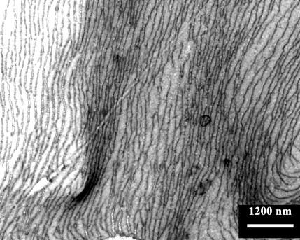
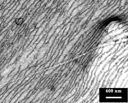
68 a c b d Figure 3.15 (a-d). Bright-field TEM micrographs of PS-b-PMMA_1 film deposited on ITO substrate and annealed at 150 C under electric field of 110 V/µm applied across the ITO electrode and an aluminum tape electrode. a c d b Figure 3.16 (a-d). Bright-field TEM micrographs of PS-b-PMMA_1 film deposited on ITO substrate and annealed at C under electric field of 110 V/µm applied across two bottom and top ITO electrodes.
69 These data can be explained considering that the preferential segregation of one block onto surface or interface originates from the difference in interfacial energies γ between the two blocks. The strength of the driving force for parallel orientation is, therefore, proportional to Δγ A-B = γ A - γ B. The electric-field-induced alignment in block copolymers is a consequence of the difference in the dielectric constants between the two constituent blocks. 26 Hence, this driving force is proportional to Δε A-B = ε A - ε B. Table 3.1 lists the dielectric constants and surface energies for the blocks of the copolymer employed in this study. Table 3.1. Dielectric constant ε and surface energy γ of PS and PMMA blocks in PS-b-PMMA. Polymer Dielectric constant, a ε (Hz) Surface energy, b γ (mn/m) Polystyrene Polymethylmethacrylate a Ku, C. C.; Liepins, R. Electrical Properties of Polymers: Chemical Principles; Hanser Publisher: Munich, Brandrup, J., Immergut, E. H., Eds. Polymer Handbook, 3rd ed.; John Wiley & Sons: New York, b When both the dielectric constant and the surface energy are very close in values, there are only weak forces in play and disordered array microdomains oriented parallel to the surface of the electrodes are possible. When the difference in the interfacial energies is large the surface field dominates aligning the microdomains parallel to the interface, despite both the surface and electric fields are acting on the microdomain alignment in two orthogonal directions. In the case of PS-b-PMMA Δε between the two blocks is higher than the difference in the interfacial energies. So, this character of PS-b-PMMA copolymer enables a strong influence by the electric field, orienting the interface in the direction of the applied electric field. It is worth noting that the application of external electric fields produces an increase of lamellar spacing that characterized our BCP. In particular, PS-b-PMMA_1 is characterized by periodicity of 30 nm that is unchanged when the applied electric field is equal to 70 V/μm. Above this value, we obtain an increase of periodicity up to 90 nm. This suggests the existence of an electric field threshold above which the periodicity increases. 69
70 3.2.2 Nanoparticles In the last few years, nanoparticles have been a common material for the development of new cutting-edge applications in communications, energy storage, sensing, data storage, optics, transmission, environmental protection, cosmetics, biology, and medicine due to their important optical, electrical, and magnetic properties. In particular, the unique properties and utility of nanoparticles also arise from a variety of attributes, including the similar size of nanoparticles and biomolecules such as proteins and polynucleic acids. 39 Additionally, nanoparticles can be fashioned with a wide range of metals and semiconductor core materials that impart useful properties such as fluorescence and magnetic behavior. 40 Nanoparticles of particular materials show unique material properties, hence, manipulation and control of the material properties via mechanistic means is needed. In addition, synthesis of nanoparticles having uniform shape and size via easy synthetic routes is the main issue in nanoparticle growth. For the past decade, scientists have been involved in the development of new synthetic routes enabling the precise control of the morphology and size of the nanoparticles. In addition, nanoparticle synthesis can be possible via liquid (chemical method), solid, and gaseous media, but due to several advantages over the other methods, chemical methods are the most popular methods due to their low cost, reliability, and environmentally friendly synthetic routes, and this method provides rigorous control of the size and shape of the nanoparticles. In general, nanoparticles with high surface-to-volume ratio are needed, but the agglomeration of small particles precipitated in the solution is the main concern in the absence of any stabilizer. In this regard, preparations of stable colloids are important for nanoparticle growth. In addition, nanoparticles are generally stabilized by steric repulsion between particles due to the presence of surfactant, polymer molecules, or any organic molecules bound to the surface of nanoparticles. Sometimes Van der Waals repulsion (electrostatic repulsion) also plays important role in nanoparticles stabilization. With all the issues related to nanoparticle synthesis, there are various types of nanoparticles reported in the literature, e.g., metal nanoparticles, metal oxide nanoparticles, and polymer nanoparticles. In this research activity we have realized gold nanoparticles by both evaporation/condensation process and chemical synthesis. We have also synthesized Zinc Oxide nanoparticles by chemical process. 70
![3.2.3 Gold Nanoparticles Gold has the atomic number 79 (electron configuration, [Xe] 4f 14, 5d 10, 6s 1 ), and is one of the so - called noble metals, which are resistant to both corrosion and](/docs-images/85/91546715/images/71-0.jpg "oxidation. Gold is the most malleable and ductile of the known elements, with characteristic properties of being dense, soft, and shiny.")

71 3.2.3 Gold Nanoparticles Gold has the atomic number 79 (electron configuration, [Xe] 4f 14, 5d 10, 6s 1 ), and is one of the so - called noble metals, which are resistant to both corrosion and oxidation. Gold is the most malleable and ductile of the known elements, with characteristic properties of being dense, soft, and shiny. Gold nanoparticles (AuNPs), which are also known as colloidal gold or nanogold, are a colloid of nanosized gold particles in a liquid (generally water). The first description of colloidal gold was reported by the philosopher and medical doctor Francisci Antonii in Subsequently, in 1676, the chemist Johann Kunckles 55 described drinkable gold that contains metallic gold in a neutral, slightly pink solution that exert curative properties for several diseases. Although colloidal gold has been known from ancient times, when it was used as for staining glass, the modern scientific development of colloidal gold did not begin until Michael Faraday s pioneering studies in the nineteenth century. In 1857, Faraday prepared a red - colored solution of colloidal gold in a two - phase system by the reduction of an aqueous solution of chloroaurate ( AuCl 4 ) using phosphorus in carbon disulfide. 56,57 The AuNPs are the most stable metal nanoparticles, and have been studied extensively during the past decade owing to their fascinating aspects in materials science, size - related electronics, and optical properties (quantum size effect), as well as their applications in catalysis and biology. This is clearly evident from a literature survey of published articles relating to AuNPs with respect to years. 58 This analysis reveals that reports on AuNPs have increased significantly each year (Figure 3.17 a), and indicates that remarkable attention - from both fundamental and applied aspects has been paid to the synthesis, characterization, and potential application of AuNPs. (b) Figure (a) Statistical survey of articles published on AuNPs, and contributions from the top ten countries in percentage for AuNPs (b). 71
72 When reducing the first, second or third dimensions (1 - D, 2 - D or 3 - D) of bulk material to the nanometer scale, nanometer - thick 2 - D layers, 1 - D nanowires, or 0 - D nanoclusters, respectively, are produced. Nanoparticles have diameters of < 100 nm and demonstrate new or enhanced size - dependent properties when compared to larger particles, or to the bulk entity of the same material. Metal nanoparticles and especially AuNPs appeared as a new class of materials which were of interest not only in the fields of materials science and chemistry but also in nanotechnology, on the basis of their exceptional catalytic, electronic, and optical properties. Notably, these features related neither to the bulk metal nor to the molecular compounds, but depended heavily on the particle size, the nature of the protecting organic shell, and the shape of the nanoparticle. 59 For example, gold nanocrystals of different shapes possess unique optical scattering responses. Whilst symmetric spherical particles display a single scattering peak, anisotropic shapes such as rods, 60 triangular prisms, 61 and cubes 62 exhibit multiple scattering peaks in the visible wavelengths due to highly localized charge polarizations at their corners and edges. With regards to metallic gold, the nucleation and growth of nanoparticles have been most widely achieved using colloidal methods rather than a variety of other approaches. 57 In these techniques, the general approach is to reduce a gold salt precursor in solution (mostly aqueous) in the presence of a stabilizing or protecting agent; this improves the chemical stability of the AuNPs formed by avoiding the aggregation among the particles. The advantages of these methods are: (i) large quantities of nanoparticles can be synthesized; (ii) solution - based processing and assembly can be readily implemented; (iii) no specialized equipment is necessary; (iv) the technique is comparatively low - cost in nature; and (v) the preparation is both facile and user - friendly. The aforesaid reasons are particularly important when considering the real applications of AuNPs; in order to utilize AuNPs as catalytic, electronic, or optical materials a large - scale synthesis and assembly process is required. It is well known that much attention has been paid to metal nanoparticles based on their pivotal applications as advanced materials in an ample diversity of areas such as catalysis, optical devices, nanotechnology, and the biological sciences Today, many applications of metal nanoparticles are close to profi table implementation, with AuNPs in particular having attracted most attention based on their potential use in applications such as catalysis, 66,67 chemical sensors, 68 biological and/or medical areas, 69,70 and the miniaturization of electronic devices due to their unique optical and electrical properties. 57 The applications of thiol-stabilized AuNPs in catalysis comprise asymmetric dihydroxylation reactions, 71 carboxylic ester cleavage, 72 electrocatalytic reductions, 73 and particle - bound ring - 72
73 opening metathesis polymerization, 74 among others. 57 These catalytic applications have in common an exploitation of the carefully designed chemical functionality of the ligand shell, rather than the potential catalytic activity of a nanostructured clean metal surface. From a biological aspect, a color change of AuNP aggregates, from ruby - red to blue, has been exploited in the development of a highly sensitive calorimetric technique for DNA analysis, capable of detecting trace amounts of oligonucleotide sequences. The same effect has also been used to distinguish between perfectly complementary DNA sequences and those exhibiting different degrees of base pair mismatches. 75 One of the most famous potential long - term applications of AuNPs is the fabrication of new (eventually small) electronic devices; 76,77 for example, a single - electron transistor action has been demonstrated for systems that contain ideally only one particle in the gap between two contacts separated by only few nanometers Nanocomposites from block copolymer ordered lamellar nanostructures and selective gold deposition. The idea of harnessing of BCP morphology as a means of creating ultra-fine ordered dispersions of inorganic particles is well established. 78 Several research initiatives have recently demonstrated that BCPs can be used to create and/or distribute nanometer-sized, metallic, magnetic, 78,81,82 and ceramic structures. A plethora of devices, such as terabit-level memory storage media, become possible if the organization of the diblock domains that house these particles can be adequately controlled. Three general strategies for patterning nanoscopic particulates in BC thin films have been explored: Surface decoration techniques involve the preferential segregation of deposited material to favored domains on a pre-oriented BCP film surface 89,90. In solution-blended composites, bare or surface-activated nanoparticles are combined with BCP in solution. During film processing, these particles sequester into preferred block domains. 91,92 A theoretical treatment of this phenomenon was published by Balazs and coworkers. 93 Finally, so-called nanoreactors use inorganic precursors, such as metal salts, engineered to preferentially associate with one component of a BCP. This can be accomplished by actually incorporating the precursor moieties as pendant groups on one of the block species in the system, 78,79 but BCP/precursor blends have also been demonstrated to work After films are cast and microphase separation occurs, the precursor molecules, now confined to one of the patterned domains, are reduced (or otherwise transformed) in 73
74 situ to form particles. Later, the polymer may be removed, leaving a nano patterned inorganic phase on the substrate. 83,95 In general, self-assembly is emerging as an elegant, `bottom-up' method for fabricating nanostructured materials 1,95, and this approach becomes particularly powerful when the ease and control offered by the self-assembly of organic components is combined with the electronic, magnetic or photonic properties of inorganic components. 98,101,103 Two important, competing, issues for the assembly of inorganic materials on organic scaffolds are high density and selectivity. In the case of scaffolds formed by copolymer domains, preferential wetting of one of the copolymer blocks by metal will selectively aggregate the metal inside the corresponding domain. 90,104 However, simple coalescence of dense metal nanoparticle aggregates into the overall shape given by the boundaries of the selected copolymer domain has not been achieved so far. This is because of the large surface energies of metals, exceeding those of copolymers by orders of magnitude. Consequently, metal-metal bonds will overwhelm metalpolymer bonds and, except for very small metal concentrations, the final configuration will be a large, spherical metal aggregate that completely ignores the polymer scaffold and mitigates selectivity. Thus, under equilibrium conditions even highly elongated, anisotropic polymer scaffolds may not be able to guide self-assembling metal particles into wire-like nanostructures. So, during the research activity we have demonstrated how non-equilibrium processes can induce, and stabilize, recognition of complex patterns provided by a nanoscale scaffold. In fact, we have investigated the possibility to use lamellar nanolayers of our block copolymer as matrix of hybrid nanocomposites through selective inclusions of metal nanoparticles in specific layers. Fabrication of samples followed a four-step process as sketched in Figure The process starts by spin coating a thin film of PS-b-PMMA_1 copolymer from a toluene solution onto a ITO substrate (Figure 3.18 a). During the first annealing step, the diblock phase separates. This produces a striped surface pattern in which both blocks alternate along the film surface 90 and form a template for the further self-assembly of metal 105 (Figures 3.18b and 3.18 e). Decoration of the film is achieved by evaporating a small amount of gold and successive condensation onto the surface of the diblock film (Figure 3.18c). This deposition was realized by a simple procedure based on evaporation and condensation under high vacuum (about mbar) of metal nanoparticles, using an Quorum Technologies K950X Turbo Evaporator. The copolymer film was positioned at a distance of 15 cm from a gold wire, which was wrapped around a tungsten filament. A voltage value slightly above the minimum needed to bring the tungsten filament to incandescence was applied for 2-3 s, to avoid melting of the polymer sample. One completes creating the samples by annealing the sample for a second time in vacuum (10-3 mbar) (Figure 3.18 d). 74
. Deposition of metal by evaporation and condensation onto diblock template (c).")
75 a a ITO PS PMMA Au e b b c c d d Figure Sketch of fabrication process. Spin coat ITO substrate with 2wt% solution of diblock in toluene (a). First annealing, microphase separate diblock film in 150 C oven in vacuum (b). Deposition of metal by evaporation and condensation onto diblock template (c). Second annealing, improve metal selectivity and diffuse metal onto diblock film by annealing in vacuum at 150 C (d). TEM image of a thin film of PS-b-PMMA_1 (e) corresponding to step b stained with RuO 4 without gold. The TEM bright-field image of thin films 70 nm thick of PS-b-PMMA_1 deposited on the ITO substrate by spin coating at room temperature, stained with RuO 4 and decorated with gold nanoparticles is shown in Figure 3.19 a. The presence of dark spots clearly indicate the formation of gold nanoparticles, having a diameter of 4 nm (Figure 3.19, b), and their deposition onto the surface of the lamellar structure of the BCP. A full selective gold decoration (with selectivity of almost 100%) has been achieved by annealing the film in vacuum at temperatures above the glass transition temperature (150 C) and below the temperature of disintegration of the templating pattern. The TEM bright field image of the thin film of Figure 3.19 annealed at 150 C is shown in Figure It is apparent that after annealing the gold nanoparticles are exclusively included into the darker stained PS microdomains. Therefore, in these conditions the deposited metal atoms diffuse onto the preferred vertically aligned PS lamellae, resulting in the formation special nanocomposite characterized by a nanostructured polymer matrix and high dispersion of gold nanoparticles which are selectively included into one of the two different lamellar microdomains of the BCP, in particular into PS microdomains. 75
 TEM bright-field image of a thin film 70 nm thick of PS-b-PMMA_1 deposited on ITO substrate by spin coating at room temperature, stained with RuO 4 and decorated with gold nanoparticles by")
76 Normalized counts a) b) Diameter of Au nanoparticles (nm) Figure (a) TEM bright-field image of a thin film 70 nm thick of PS-b-PMMA_1 deposited on ITO substrate by spin coating at room temperature, stained with RuO 4 and decorated with gold nanoparticles by thermal vacuum evaporation and condensation. (b) Typical size distribution of Au-NPs obtained by measuring the diameter of at least 100 nanoparticles in TEM micrograph. Moreover, a disordered but regular close-packed clustering of Au-NPs over a large area is observed thanks to the host homogeneous phase-separation into randomly oriented, but regularly sized, PS and PMMA nanodomains. This is also well shown in SEM micrograph reported in Figure


77 Figure TEM bright-field image of a thin film 70 nm thick of PS-b-PMMA_1 deposited on ITO substrate by spin coating at room temperature, stained with RuO 4, decorated with gold nanoparticles by thermal vacuum evaporation and condensation, after annealing at 150 C for 6h under vacuum. The inset shows the image with higher magnification. Figure SEM image of a thin film 70 nm thick of PS-b-PMMA_1 deposited on ITO substrate by spin coating at room temperature, decorated with gold nanoparticles by thermal vacuum evaporation and condensation, after annealing at 150 C for 6h under vacuum. 77
78 The selective inclusion of gold nanoparticles into the PS microdomains is in agreement with the results of ref. 106 in the case of PS-b-PMMA diblock copolymer with cylindrical morphology. As argued in ref. 106b, before annealing gold nanoparticles are on the top of the diblock film and their average distance are quite large (see Figure 3.20). Upon annealing the nanoparticles most likely diffuse into the film and find a place within the block that is energetically most favorable. As shown in Figure 3.20, the most favorable position is clearly within the PS-rich regions of the film. It is worth noting that a slight modification of the lamellar morphology of Figures 3.11 and 3.12 occurs after infiltration of gold nanoparticles (Figure 3.20). The images of Figure 3.11 and 3.12 display clear short-range ordering and measurable lamellar spacing, whereas domains of figure 3.20 are larger and rather random. This indicates that the morphology is slightly modified after inclusion of gold nanoparticles that diffuse into PS domains producing their enlargement. The results of Figures 3.11, 3.12, 3.20 and 3.21 clearly indicate that the rational choice of neutral substrates complemented with the technique of gold decoration is a simple route for controlling the surface behavior of the BCP and the nanodomains orientation and for preparing special nanocomposites characterized by selective inclusion of nanoparticles in target microdomains of the nanostructure. We have than evaluated the possibility to induce long range order to these hybrid nanostructures by technique of external electric fields mentioned in paragraph Following the same procedures for application of external electric fields coupled with thermal annealing and selective inclusion of NPs described before, gold nanoparticles were this time guided by the BCP under electric field-assisted annealing. So, thin films of PS-b-PMMA film were deposited on ITO substrate, decorated with Au-NPs and annealed at 150 C under electric field of 110 V/µm. The host guiding effect allowed clustering the metal atoms preferentially along the parallel PS stripes producing periodic alternating Au-NPs-enriched PS stripes and Au-NPs-depleted PMMA stripes, i.e. vertical stacks, or nano-walls, of gold nanoparticles. This is clearly evident in the TEM image of Figure 3.22 and the related inset, which shows that Au-NPs mainly fill the darker stained PS layers (with selectively higher that 70 %). The average spacing of PS lamellae is estimated to be 27 nm after inclusion of the gold atoms as shown in the following bar diagram (Figure 3.23) evaluated from the Figure


79 Number of PS lamellae (%) Figure Bright-field TEM micrograph of PS-b-PMMA_1 film deposited on ITO substrate, stained with RuO 4, decorated with Au-NPs and annealed at 150 C under electric field of 110 V/µm (d). The inset is a close-up of image Size of PS lamellae (nm) Figure Bar diagram and its fitting curve representing the size of PS lamellar domains after inclusion of AuNPs evaluated from the TEM image. Clearly these procedures allow obtaining nanocomposites characterized by a structureguiding host-patterning based on selective inclusion of gold nanoparticles in target nanodomains of 79
80 DSC endotherm a block copolymer matrix, with no need of ligand-coated nanoparticles. The formation of ordered gold nanostructures is guided by the self-assembly of the block copolymer. The PS and PMMA phase-separated lamellae of the self-assembling PS-b-PMMA block copolymer have vertical interfaces that align with long-range parallel fringes by applying a static electric field during thermal annealing. Gold nanoparticles are simply produced by vacuum evaporation of gold and successive deposition onto the film surface of the phase-separated block copolymer, and, after thermal annealing, result selectively included only into the PS layers. Monodisperse Au-NPs are guided to cluster into PS domains following the BCP host morphology. These materials were used as SERS substrates; corresponding characterizations are reported in successive chapter IV. 3.3 Characterization of nanocomposites based on PS-b-PMMA block copolymer with cylindrical morphology and gold nanoparticles obtained by chemical synthesis Thermal analysis of neat PS-b-PMMA The DSC cooling and heating curves, recorded at 10 C/min of the sample of PS-b-PMMA_2, are reported in Figure The BCP sample presents glass transition temperatures of the PS and PMMA blocks of 107 C and 132 C, respectively. Cooling Heating Tg (PS) Tg (PMMA) Temperature ( C) Figure DSC heating and cooling curves of the sample of PS-b-PMMA_2. 80


81 3.3.2 Morphological analysis of the neat PS-b-PMMA As reported in Chapter II, we have also studied morphological properties of PS-b-PMMA_2 (M n (PS)=47.4 Kg/mol, M n (PMMA) = Kg/mol, molecular mass distribution M w /M n = 1.11, and volume fraction of PS block equal to 0.28) able to give by self-assembly a cylindrical microphase-separated morphology with the PS blocks forming a hexagonal array of cylinders in the PMMA matrix. Thin films of PS-b-PMMA_2 65 nm thick were obtained by spin-coating at room temperature, after deposition of a slight excess toluene BCP solutions on glass substrate. Also in this case, these films were stained with RuO 4 for TEM analysis in order to achieve a good contrast between PS and PMMA domains. The TEM bright field image of the stained film is shown in Figure 3.25 a. The dark regions correspond to the stained PS cylindrical microdomains that are disorderly dispersed in the PMMA matrix (lighter regions in Figure 3.25 a). The PS cylinders are mainly oriented with the axes parallel to the film surface, as schematically shown in Figure 3.25 b. a) b) Figure (a) TEM bright-field image of a thin films 65 nm thick of PS-b-PMMA_2 (stained with RuO Figure 1. (a) TEM bright-field image of a thin films 65 nm thick of PS- b -PMMA (stained with RuO 4 ) 4 ) obtained at room temperature on a glass substrate by spin coating at 4000 rpm for 30 s a slight excess of a 2wt% BCP/toluene solution. In (a) the PS cylinders are oriented with their axes almost parallel to the glass substrate, as shown in 81 the schematic model (b).
82 Number of PS cylinders (%) The thickness of PS domains is 20 nm, as reported in the following Figure Size of PS cylinders (nm) Figure Bar diagram and its fitting curve representing the size of PS cylinders domains Synthesis of Thiol-derivatised Gold Nanoparticles As widely cited in previous paragraphs, the different microdomains of BCP nanostructures (spheres, cylinders or lamellae) can act as hosts for sequestering metal nanoparticles of appropriate chemical affinity and geometry. In this approach the nanostructured block-copolymer matrix act as a structure-guiding matrix, where the nanoparticles are sequestered into target microdomains of the BCP structure, resulting in an ordered spatial positioning of the guest particles guided by the ordering of the host matrix and a hierarchical assembly of organic-inorganic (polymer-metal) nanostructures, in which one level of self-assembly guides the next. This ability makes BCPs ideal as scaffolds for the engineering of new materials characterized by patterned surfaces, and controlled and ordered assembly of metal nanoparticles. Various strategies were described in the literature for achieving the selective infiltration of nanoparticles in specific microdomains of the ordered nanostructure, as, for instance, the in-situ synthesis of nanoparticles during phase separation of BCPs, or ex-situ synthesis and successive coassembly of BCP and nanoparticles. 107 In these strategies the surface of the metal nanoparticles are generally modified to improve chemical affinity with the target microdomains of the BCP nanostructure, and to prevent their self-aggregation, for instance by attaching oligomer chains to the 82
83 particle surface that will favorably interact with the more affine target domains during the selfassembly process. 107 We have synthesized gold nanoparticles bearing on the surface 2-naphthylthiolate (NT) units (NT-AuNPs) (Figure 3.27) using the method of Brust et. al. 108 The strategy followed consisted in growing the metallic clusters with the simultaneous attachment of self-assembled thiol monolayers on the growing nuclei. In order to allow the surface reaction to take place during metal nucleation and growth, the particles were grown in a two-phase system. Two-phase redox reactions can be carried out by an appropriate choice of redox reagents present in the adjoining phases. In the present case, AuC1-4 was transferred from aqueous solution to toluene using tetraoctylammonium bromide as the phase-transfer reagent and reduced with aqueous sodium borohydride in the presence of naphthalenethiol (C 10 H 7 SH). On addition of the reducing agent, the organic phase changes colour from orange to deep brown within a few seconds. The overall reaction is summarized by following equations, where the source of electrons is BH - 4. The conditions of the reaction determine the ratio of thiol to gold, i.e. the ratio n/m. AuC1 4 - (aq) + N(C 8 H 17 ) 4 + (C 6 H 5 Me) N(C 8 H 17 ) 4 + AuCl 4 - (C 6 H 5 Me) mauc1 4 - (C 6 H 5 Me) + nc 10 H 7 SH(C 6 H 5 Me) + 3me - 4mCl (aq)+(au m )(C 10 H 7 SH) n (C 6 H 5 Me) S S AuNP S S Figure Structure of Au nanoparticle bearing on the surface 2-naphthylthiolate (NT) units. 83
84 Weight (%) The preparation technique was as follows. An aqueous solution of hydrogen tetrachloroaurate (HAuCl 4 ) (10 ml, 30 mmol dm -3 ) was mixed with a solution of tetraoctylammonium bromide (N(C 8 H 17 ) + 4 Br - ) in toluene (30 ml, 50 mmol dm -3 ). The two-phase mixture was vigorously stirred until all the tetrachloroaurate was transferred into the organic layer and naphthalenethiol (48 mg) was then added to the organic phase. A freshly prepared aqueous solution of sodium borohydride (NaBH 4 ) (8 ml, 0.4 mol dm -3 ) was slowly added with vigorous stirring. After further stirring for 3 h the organic phase was separated, evaporated in a rotary evaporator and mixed with 30 ml ethanol to remove excess thiol. The dark brown precipitate was filtered off and washed with dichloromethane. The liquid phase is removed by compressed air. We have valuated the obtainment of NT-AuNPs by thermogravimetric, spectrophotometric and TEM analysis as follows Thermogravimetric analysis of nanoparticles (NT-AuNPs) Thermogravimetric profil of NT-AuNPs is reported in figure The analysis reveals a weigh loss equal to 17% between 180 C and 295 C. The final residual is equal to 77%. This weight loss is due to degradation of organic phase constituted by naphthalenethiol (NT), while the residual corresponds to AuNPs % % 77.32% Residual 77.17% (1.742 mg) Temperature ( C) Figure Thermogravimetric curve of NT-AuNPs. 84
85 Abs UV-Vis spectra measurements of nanoparticles (NT-AuNPs) UV-Vis spectrum of NT-AuNPs in toluene solution is reported in Figure Comparison between this spectrum and literature data 108 allows to evaluate the effective formation of nanoparticles. This spectrum of gold nanoparticles shows a maximum a with a broad band around 506 nm. This value is in agreement with literature data, that suggests the formation of NT-AuNPs. 0,8 0,7 506 nm 0,6 0,5 0,4 0,3 0, Wavelength (nm) Figure UV-Vis spectrum of NT-AuNPs in toluene solution TEM analysis of nanoparticles (NT-AuNPs) We have prepared NT-AuNPs nanoparticles for TEM analysis by dipping of copper grid with Formvar support (300 mesh) into a dilute toluene solution of these nanoparticles (0.5 mg/ml) for few seconds. TEM bright-field image of nanoparticles is reported in Figure 3.30 a. NT-AuNPs show a average diameter of 3 nm evaluated from TEM analysis (Figure 3.30 b). This value was calculate by measuring the diameter of at least 100 nanoparticles in TEM micrograph. 85
. 3.")
86 Normalized Counts a) b) 1,0 1,2 1,4 1,6 1,8 2,0 2,2 2,4 2,6 Diameter of NT-Au nanoparticles (nm) Figure TEM bright-field image of Au nanoparticles covered with NT units (a). Typical size distribution of NT- AuNPs obtained by measuring the diameter of at least 100 nanoparticles in TEM micrograph (b) Nanocomposites based on PS-b-PMMA and NT-AuNPs with long range order The obtainment of gold nanoparticles bearing on the surface 2-naphthylthiolate (NT) units, allows obtaining selective inclusion of these nanoparticles in specific domains. In particular, the presence of NT units favors the chemical affinity of the nanoparticles with the PS domains of PS-b- PMMA and affords opportunity for having an electric-field-induced charge transfer mechanism in the same nanoparticle to be exploited for building electronic devices with memory functions. 109 As reported in Chapter I, paragraph 1.3, the ideal ordered nanostructure that will act as host matrix for the selective inclusion of gold nanoparticles should be characterized by PS cylinders aligned with their axes normal to the film surface. Solvent evaporation under controlled conditions can provide a strong directional field to orient block copolymer film nanostructures. 110 A high degree of lateral order with few defects can be achieved. This results from the propagation of ordering from the surface into the film. It may also enable ordered structures to develop more rapidly, although equilibrium morphologies may not be accessed without further annealing. Krausch and co-workers showed that the solvent (THF) evaporation rate could be used to change the orientation of lamellae formed by a PS P2VP PtBMA 86
87 [(P2VP = poly (2-vinylpyridine and PtBMA= poly (tert-butyl methacrylate)] triblock copolymer. 111 It was further shown that macroscopic sample geometries (confinement within channels) could be used to enhance alignment due to the anisotropic lateral contraction induced. Parallel lamellae were observed for low evaporation rates, and perpendicular lamellae for high evaporation rates. Russell and co-workers have applied the solvent annealing technique very successfully to PS PEO films annealed in benzene vapor. 112 GISAXS has been used to probe the development of ordering and the perfection of the hexagonal structure has been quantified via triangulation algorithms. For PS PEO diblocks, environment-controlled spin-coating in a mixed solvent atmosphere of toluene and water leads to well-developed perpendicular PEO cylinder orientation. 113 Toluene is a selective solvent for PS, whereas water is selective for PEO. Perpendicular orientation was favored in the presence of a mixture of solvents selective for each block. In contrast, Xuan et al. suggest that well-ordered cylinders form in thin films in the presence of a PMMA-selective solvent (chloroform or acetone) only. Following extended solvent vapor treatment, the parallel cylinder morphology is recovered with PMMA at the surface instead of PS. It has been mentioned that solvent annealed structures can be subjected to aging, in particular interfacial flattening, due to interfacial tension. 114 Addition of salt has been shown to improve the ordering of perpendicular PEO cylinders in a PS PEO diblock film during solvent annealing. 115 Complexation of the alkali halide or metal salts with PEO leads to greater incompatibility between blocks and enhanced mobility of the polymer chains, both contributing to the improvement in ordering. Annealing in selective solvents can lead to non-equilibrium structures in PS-b-PMMA diblocks. 116 Annealing of either a symmetric or an asymmetric sample in a selective solvent for PMMA (acetone) created initial hexagonal-packed sphere structures, which upon further exposure to solvent developed into the expected stripe patterns resulting from lamellar or cylinder structures. The non-equilibrium hexagonal structures can be trapped by vitrification at room temperature. Annealing in different solvents can be used to switch from parallel to perpendicular cylindrical P4VP + HABA (HABA = (2-(4 -hydroxybenzeneazo)benzoic acid) domain orientation and vice versa in thin films of PS P4VP complexed with HABA. 117 The HABA forms a hydrogen bonding complex with the P4VP. Swelling in dioxane even led to a transition to a spherical morphology. The polymer-solvent interaction parameter χ was taken into account to evaluate the miscibility between a polymer and a solvent and in our case χ was calculated in order to quantify the affinity between the blocks constituting the PS-b-PMMA copolymer and the vapors of different solvents. This parameter is modeled as the sum of entropic and enthalpic components: 87
88 (eq. 1) where χ H is the enthalpic component and χ S is the entropic component. χ S is usually taken to be a constant between 0.3 and 0.4 for nonpolar systems: χ S = 0.34 is often used. 118 The enthalpic component can be related to the Hildebrand parameters: [ ( ) ] (eq. 2) with V i the molar volume of species, δ 1 and δ 2 the Hildebrand parameters of the interacting polymer and solvent, R the ideal gas constant at temperature T. Substituting eq. (2) in eq. (1): [ ( ) ] (eq. 3) Equation (3) permits only positive values of the interaction parameter. Since the Flory- Huggins criterion for complete solvent-polymer miscibility is χ < 0.5, the enthalpic contribution must be small and the solubility parameters of the solvent and polymer must be similar. The molar volume of the solvent also affects miscibility and phase equilibria: a Hildebrand parameter needed for phase separation or miscibility cannot be specified without specifying Vi. Equation (3) works well for nonpolar systems for which Eq. (2) is a good description of the enthalpic component of the interaction parameter. The geometric mean assumption of regular solution theory is not appropriate for polar systems, and better models include an extra term describing the interchange energy density for the solvent-polymer pair. For example: ( ) (eq. 4) with: (eq. 5) where l 12 characterizes the intermolecular forces between molecules (rather than using the geometric mean assumption). Equation (5) allows the modeling of specific interactions between components 1 and 2. Mixed solvents can be treated as a single solvent by determining the solubility parameter of the solvent mixture, and then using this value in Eq. (3). If both the solvents and the 88
89 polymers interact, the description is more complicated. An alternative definition of A12 uses the two-component solubility parameter: ( ) ( ) (eq. 6) with δ d is the dispersion solubility parameter, and δ p is the polar solubility parameter. 116,119,120 The Hansen parameters may also be used to model A 12. From these considerations the χ values for different considered polymer-solvent pair were calculated as reported in Table 3.2. Table 3.2. Polymer-solvent interaction parameter for the PS block [χ p-s (PS)] and for PMMA block [χ p-s (PMMA)]. Solvent p-s (PS) p-s (PMMA) dichloromethane ,2-dichloroethane acetone n-hexane ethanol isopropanol Methylethylketone Previous study have demonstrated that dichloromethane is theta solvent for PS and good solvent for PMMA. 121 The following parameters were calculated for this solvent (table 3.3): Table 3.3. Molar volume (Vs) and Hildebrand parameter (δ) for solvent and polymers. Solvent/Polymer V s (cm 3 /mol) δ (J/cm 3 ) δ (J/cm 3 ) dichloromethane PS 18.6 PMMA Thin films of hybrid nanocomposites consisting of PS-b-PMMA_2 and NT-AuNPs were prepared by spin coating a toluene solution containing 2 wt% PS-b-PMMA_2 and different 89
 and successive exposition at room temperature to dicholoromethane vapors at different times (20 minutes and 60 minutes), to induce a high degree of perpendicular orientation of PS cylinders")
, at different concentration of NT-AuNPs without RuO 4 staining, typically show a high contrast of dark PS cylinder with respect to PMMA matrix.")
90 concentration of NT-AuNPs (0.1wt%, 0.2wt%, 0.3wt%) and successive exposition at room temperature to dicholoromethane vapors at different times (20 minutes and 60 minutes), to induce a high degree of perpendicular orientation of PS cylinders over large areas. TEM bright field images of the so obtained thin films (Figures 3.31 a, b, c), at different concentration of NT-AuNPs without RuO 4 staining, typically show a high contrast of dark PS cylinder with respect to PMMA matrix. The result that the PS cylinders appears dark without RuO 4 staining is a clear indication that gold nanoparticles are not dispersed in the whole BCP, but were selectively included in the PS cylinders. The uniform inclusion of AuNPs in the PS domains is achieved thanks to the designed chemical modification of the nanoparticles surface with naphthalene-thiolate (NT) units. The coating agent was specifically identified in order to achieve a high affinity for PS cylinders and less affinity for the PMMA matrix. The selective and uniform inclusion of NT-AuNPs in the target PS cylinders is clearly demonstrated by the TEM images of Figure 3.31 (a, b, c) of BCP films containing nanoparticles taken over various areas and on independently prepared films. TEM images clearly shown that a good degree of perpendicular orientation of PS cylinders was achieved by exposing films of PS-b-PMMA_2 for 60 min at room temperature to vapors of dichloromethane, which has a good affinity for both blocks. This is schematically represented in Figure 3.31 d. a) CH 2 Cl 2 vapours T room, 20 min 90


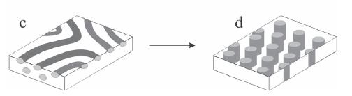
91 b) CH 2 Cl 2 vapours c) T room, 20 min CH 2 Cl 2 vapours T room, 60 min d) CH 2 Cl 2 vapours T room, 60 min 91
 TEM bright field images of thin films 65 nm thick of PS-b-PMMA_2 based nanocomposite obtained on a glass substrate by spin coating at 4000 rpm for 30s a slight excess of a toluene solution")
92 e) Figure (a, b, c) TEM bright field images of thin films 65 nm thick of PS-b-PMMA_2 based nanocomposite obtained on a glass substrate by spin coating at 4000 rpm for 30s a slight excess of a toluene solution containing 2wt% BCP and 0.1wt% (a), 0.2wt% (b) and 0.3wt% (c) NT-AuNPs respectively, drying at room temperature and successive exposition at room temperature to dicholoromethane vapors for 20 and 60 min. (d) After exposure to dichloromethane vapors the PS cylinders orient with their axes perpendicular to the substrate. (e) A cartoon showing how NT-AuNPs are selectively included in PS domains. These images clearly indicate that practically all PS cylinders are filled with Au nanoparticles (Figure 3.31 e). Nanocomposites based on PS-b-PMMA_2 and NT-AuNPs can be used as active layers within opotoelectronic devices, such as memory devices. 3.4 Nanocomposites from block copolymer cylindrical nanostructures and selective gold deposition Following the same procedure described in paragraph 3.2.3, we have realized nanocomposites based on PS-b-PMMA_2 block copolymers with cylindrical morphology and gold nanoparticles obtained by the evaporation/condensation process. Again this approach affords dispersion of gold guest nanoparticles in an already nanostructured polymeric matrix, composed of preordered nanostructures formed by BCPs. The gold nanoparticles were selectively included and dispersed in the PS microdomains by using a vacuum deposition method followed by annealing in vacuum. Also in this case, this selective gold deposition results in the formation of nanocomposites characterized by high dispersion and ordered positioning of gold nanograins. The method relies on three key features: (a) the use of PS-b-PMMA_2 BCP characterized by PS cylinders dispersed in PMMA matrix; (b) obtainment of thin films on ITO substrate; (c) the 92

93 selective inclusion of gold nanoparticles in the PS microdomains by vacuum deposition and successive annealing, onto the film surface of the phase separated BCP. Thin films of PS-b-PMMA_2 were obtained by spin-coating at room temperature, after deposition of a slight excess toluene BCP solutions on ITO substrate. These films were stained with RuO 4 for TEM analysis in order to achieve a good contrast between PS and PMMA domains. The TEM bright field image of the stained film is shown in Figure The dark regions correspond to the stained PS cylindrical microdomains that are disorderly dispersed in the PMMA matrix (lighter regions in Figure 3.32). The PS cylinders are mainly oriented with the axes parallel to the film surface. Figure TEM bright-field image of a thin films of PS-b-PMMA_2 (stained with RuO 4 ) obtained at room temperature on a ITO substrate by spin coating at 4000 rpm for 30 s a slight excess of a 2wt% BCP/toluene solution. These films were decorated with gold nanoparticles by a vacuum deposition method. The deposition of gold particles on the surface of the copolymer film was realized by thermal evaporation of gold and condensation under high vacuum. Decoration of copolymer is already apparent immediately after metal deposition (Figure 3.33, a). Selectivity of 100% is achieved by warming the system in vacuum to a temperature that is above the copolymer glass transition temperature, but below the point at which the template pattern disintegrates (Figure 3.33, b). So, the preferred domain becomes the scaffold. 93
 TEM bright-field image of a thin film of PS-b-PMMA_2 with cylindrical morphology deposited on ITO substrate by")
 after annealing at 150 C for 6h under vacuum (b).")

94 a) b) Figure (a) TEM bright-field image of a thin film of PS-b-PMMA_2 with cylindrical morphology deposited on ITO substrate by spin coating at room temperature, stained with RuO4 and decorated with gold nanoparticles by thermal vacuum evaporation and condensation, and of a thin film prepared as in (a) after annealing at 150 C for 6h under vacuum (b). The inset shows the image with higher magnification. TEM images clearly shown that gold nanoparticles diffuse into preferred domains, that are darked PS domains in Figure 3.33 b. Inside the preferred domain, this leads to a coarsening that increases both the size and the separation of the nanoparticles while the metal also diffuses into the domains. 94
95 This approach is a simple method for the preparation of structure-guiding host nanocomposites in which the distribution of the guest particles is guided by host nanostructured block copolymer matrix, resulting in selective inclusion of metal nanoparticles in target microdomains without the synthesis of ligand-coated nanoparticles. 3.5 Characterization of nanocomposites based on PS-b-PMMA block copolymer with lamellar morphology and zinc oxide nanoparticles obtained by chemical synthesis ZnO NPs: crystal structure Metal oxide nanoparticles stand out as one of the most versatile materials, due to their diverse properties and functionalities. Most preferentially, among different metal oxide nanoparticles, zinc oxide (ZnO) nanoparticles have their own importance due to their vast area of applications, e.g., gas sensor, chemical sensor, bio-sensor, cosmetics, storage, optical and electrical devices, window materials for displays, solar cells, and drug-delivery ZnO is an attractive material for shortwavelength optoelectronic applications owing to its wide band gap 3.37 ev, large bond strength, and large exciton binding energy (60 mev) at room temperature. As a wide band gap material, ZnO is used in solid state blue to ultraviolet (UV) optoelectronics, including laser developments. In addition, due to its non-centrosymmetric crystallographic phase, ZnO shows the piezoelectric property, which is highly useful for the fabrication of devices, such as electromagnetic coupled sensors and actuators. 127 Crystalline ZnO has a wurtzite (B4) crystal structure at ambient conditions. The ZnO wurtzite structure has a hexagonal unit cell and belongs to the space group of P6 3 mc. Figure 3.34 clearly shows that the structure is composed of two interpenetrating hexagonal closed packed (hcp) sublattices, in which each consist of one type of atom (Zn or O) displaced with respect to each other along the threefold c-axis. It can be simply explained schematically as a number of alternating planes stacked layer-by-layer along the c-axis direction and composed of tetrahedrally coordinated Zn 2+ and O 2. The tetrahedral coordination of ZnO gives rise to the noncentrosymmetric structure. In wurtzite hexagonal ZnO, each anion is surrounded by four cations at the corners of the 95

96 tetrahedron, which shows the tetrahedral coordination and hence exhibits the sp 3 covalent-bonding. The detailed properties of ZnO are presented in Table 3.4. Figure The hexagonal wurtzite structure model of ZnO. The tetrahedral coordination of Zn-O is shown. O atoms are shown as larger white spheres while the Zn atoms are smaller brown spheres. Table 3.4. Physical properties of ZnO. Properties ZnO Lattice parameters at 300 K a 0 (nm) c 0 (nm) c 0 /a (1.633 ) Density (g/cm 3 ) Stable phase at 300 K Wurtzite Melting point ( C) 1975 Thermal conductivity (Wcm 1 C 1 ) 0.6, Linear expansion coefficient ( C) a0: 6.5 cm c0: 3.0 cm Static dielectric constant Refractive index Band gap (RT) ev Band gap (4 K) ev Exciton binding energy (mev) 60 Electron effective mass 0.24 Electron Hall mobility at 300 K (cm 2 /Vs) 200 Hole effective mass 0.59 Hole Hall mobility at 300 K (cm 2 /Vs)
97 3.5.2 Applications of ZnO NPs Regarding ZnO nanoparticle application in solar cells, Suliman et al. 128 reported the synthesis of ZnO nanoparticles with average diameter of 30 nm by using zinc chloride as a precursor and NaOH as a base in a PVP solution of water at 160 C for 8 h via the hydrothermal method. To make a ZnO film over transparent conducting glass (TCO), ZnO nanoparticles were dissolved in ethanol and then applied over the TCO surface using the doctor blade technique, which resulted in a 6 μm thick film of ZnO nanoparticles over the TCO, and finally it was annealed for 30 min at 450 C. To make dye-sensitized ZnO thin films, the film was soaked in 0.5 mm ethanol solution of ruthenium complex, cis bis(isothiocyanato) bis(2,2 -bipyridyl-4,4 -dicarboxylato) ruthenium (II) (N 3 dye). The TCO acted as a counter electrode on which 340 nm thick layer of Pt was deposited by sputtering. Recently, Zhang et al. 129 reported the synthesis of polydisperse aggregated ZnO nanocrystals and their application in dye-sensitized solar cells. In a typical synthetic process, ZnO aggregates were synthesized via polyol-mediated precipitation by using zinc acetate in diethylene glycol at 160 C with refluxing. It was reported that with adjustment in zinc acetate concentration, rate of heating, and the amount of stock solution that is added, one can readily control the size of individual ZnO aggregates. To make a photoelectrode films, ZnO aggregates were deposited by drop-cast method on a fluorinedoped tin oxide (FTO) glass substrate, and thickness of films depended on the number of drops. Finally, the ZnO films were heated at 350 C in air for 1 h to remove residual organic chemicals. Regarding the application of ZnO nanoparticles in photocatalytic activity, Houskova et al. 130 reported the synthesis of zinc sulfide (ZnS) nanoparticles by homogenous hydrolysis of zinc sulfate and thioacetadmide (TAA) at 80 C and then its conversion to ZnO nanoparticles with annealing at temperature above 400 C in an oxygen atmosphere. Xu et al. 131 reported the synthesis of hierarchically assembled porous ZnO nanoparticles through a self-assembled pathway using surface-modified colloidal ZnO nanocrystals as building blocks and P-123 copolymers as the template in aqueous solution. Functionalized ZnO nanoparticles that show liquid-like behavior were synthesized and their PL properties were reported by Bourlinos et al. 132 First, ZnO nanocrystals (3 7 nm) were prepared by alkaline hydrolysis of zinc acetate in the presence of LiOH H 2 O in absolute ethanol for 4 5 days. As-prepared ZnO colloid was precipitated by adding excess of heptane, followed by centrifugation and drying at room temperature. Surface modification of ZnO nanoparticles with charged organosilane [(CH 3 O) 3 Si(CH 2 ) 3 N + (CH 3 )(C 10 H 21 )Cl ] was carried out in an alkaline environment. The Cl counter anions in the nanosalts could be readily exchanged by - C 9 H 19 -C 6 H 4 -(OCH 2 CH 2 ) 20 O(CH 2 ) 3 SO 3 ions, yielding the corresponding sulfonate nanosalt as a 97
98 waxy solid that melts at 30 C, resulting in a fluid with considerably higher viscosity than the corresponding potassium sulfonate salt. Regarding the use of ZnO nanoparticles for sensor applications, Baruwati et al. 133 reported the hydrothermal synthesis of high-crystalline ZnO nanoparticles by using zinc nitrate as a precursor and ammonium hydroxide as a base at 120 C for 6 24 h, which were further used in sensing liquefied petroleum gas (LPG) and ethanol (EtOH). Recently, Cao et al. 134 reported methanal and xylene sensors at relatively low working temperatures. ZnO nanoparticles were prepared by a solidstate chemical reaction between zinc chloride and NaOH under ambient conditions. ZnO nanoparticles were synthesized using various routes. The various applications of ZnO nanoparticles depend upon the control of both physical and chemical properties such as size, size dispersity, shape, surface state, crystal structure, organization onto a support, and dispensability. In addition, these factors mainly depend upon the synthetic method. Therefore, shape, size, and dispersity can be controlled by tuning different parameters during the synthesis process, e.g., the precursor type and concentration, types of capping molecule, types of solvent, reaction time, and reaction temperature. Although there are various reports regarding ZnO nanoparticles with various shapes and sizes, there is still a lack of quality synthesis in terms of crystallinity, size, and sphericity of the particles and the non-use of organic solvents (which may hinder its possible application in biomedical sciences). ZnO nanoparticles used in cosmetic applications also require nonphotocatalytic activity, which can be hindered by the uniform surface coating of ZnO nanoparticles by silica or other molecules, and toxicity to the human skin is also a main concern. Application of ZnO nanoparticles in the biological realm requires high quality ZnO nanoparticles in aqueous solution at neutral ph and physiological temperature, because biomolecules are very sensitive to changes in temperature and ph. In addition, relatively small size, ease of transport within tissues/organs, ability to cross plasma membranes, and potential targeting of biologically active molecules will facilitate biomedical applications of nanoparticles in the field of medicine. At a conceptual level, we need a better understanding of the relationship between size, shape, and structure of zinc oxide nanoparticles, and how one can tune its capability for electronic and chemical interaction with biological molecules and its sensing (biological and chemical) properties ZnO Nanocrystals by a Non-hydrolytic Route Developments in the synthesis of II-VI semiconductor nanoparticles have recently demonstrated the potential of the thermal decomposition of organometallic precursors in 98
99 coordinating solvents 135 to prepare high-quality metal oxide nanocrystals. 136,137 A high-temperature synthesis of trioctylphosphine oxide (TOPO) and amine capped ZnO nanocrystals, using diethylzinc as metal precursor, has also been reported. 138 However, the use of less toxic and more easily handy precursors would be of valuable technological interest to allow a scale-up of nanocrystal synthesis. In collaboration with CNR (National Research Centre) of Bari (Italy) we have adopted an alternative preparation of organic-capped ZnO nanocrystals by the thermal decomposition of zinc acetate (ZnAc 2 ) in a high-temperature coordinating mixture of a long-chain alkylamine and tertbutylphosphonic acid (TBPA). The variation of the TBPA/ZnAc 2 molar ratio allows the tuning of the nanocrystal size in the range 2-9 nm. In this method, the addition of the phosphonic acid is important in relation to its effectiveness in directing ZnO crystal growth in the quantum confinement regime. The role of the surface in the emission properties of the nanoparticles and the stability of amine/tbpa-coated ZnO nanocrystals are also important. ZnO nanocrystals were directly grown in alkylamines by slowly heating the reaction mixture to high temperatures according to the following procedure: mmol of ZnAc 2 was dissolved in 5-10 g of an alkylamine-tbpa mixture at 80 C, and then degassed under vacuum for 1 h under vigorous stirring. The reaction vessel was then slowly heated under nitrogen at a rate of 10 C/min to induce the decomposition of ZnAc 2 ; the temperature at which the first ZnO absorption features were detected was fixed as the temperature for further growth (Tgr). Tgr generally lay in the range of C, depending on TBPA/ZnAc 2 molar ratio (R). The extraction procedures were subsequently performed in air: ZnO nanocrystals were readily precipitated upon addition of ethanol to the reaction mixture at 50 C before solidification took place. The resulting precipitate was isolated by centrifugation and was washed twice with ethanol to remove residual surfactants. The surfactant-coated ZnO nanoparticles were then easily re-dispersed in solvents such as CHCl 3 or hexane, without any further growth or irreversible aggregation, and used for spectroscopic measurements and TEM investigations. ZnO particles were grown in n-hexadecylamine (HDA) by using the slow heating method described above. The presence of tert-butylphosphonicb acid (TBPA) could guarantee the controlled growth of ZnO crystals in the nanoscopic regime. When TBPA was used as stabilizer, the growth kinetics of ZnO nanocrystals exhibited some unique characteristics. After an induction period (of a few minutes), depending on TBPA/ZnAc 2 molar ratio (R), the optical features of ZnO were detected, after which growth was seen to proceed rapidly (generally within 5-6 min), and it finally slowed considerably. Precipitation of ZnO nanocrystals in the reaction vessel was observed only after long reaction times (>2 h) and only at R <
100 Abs Optical end morphological characterization of ZnO NPs By UV-Vis measurements is possible to estimate the diameter of ZnO nanoparticles that depends to absorption position peak in the spectrum. 139 Figure 3.35 shown the UV-vis absorption spectrum of ZnO NPs obtained at TBPA/ZnAc 2 ratio equal to 0.5. We can assume an average diameter of 2 nm about from absorption position peak. The morphology of nanoparticles was evaluated by TEM analysis. Nanoparticles prepared at TBPA/ZnAc 2 ratio of 0.5 (Figure 3.36) exhibit a nearly spherical shape and a narrow size distribution (Figure 3.36 b). Moreover the diameter of this nanoparticles is equal to 2.1 nm that is in agreement with previous UV-Vis datum. 0,6 0,5 0,4 0,3 0,2 0,1 0, Wavelength (nm) Figure Absorption spectra of fully grown ZnO nanoparticles prepared with TBPA/ZnAc 2 ratio of
 Typical size distribution of ZnO NPs obtained by measuring the diameter of at least 100 nanoparticles in TEM micrograph. 3.5.")
101 Normalized Counts 1,0 1,2 1,4 1,6 1,8 2,0 2,2 2,4 2,6 2,8 3,0 3,2 3,4 Diameter of ZnO NPs (nm) Figure (a) TEM bright-field image of ZnO nanoparticles covered with HDA. (b) Typical size distribution of ZnO NPs obtained by measuring the diameter of at least 100 nanoparticles in TEM micrograph Nanocomposites based on lamellar PS-b-PMMA and ZnO NPs The obtainment of zinc oxide nanoparticles covered with hexadecylamine, allows to realize nanocomposites in which these nanoparticles are selectively included in specific domains of lamellar diblock copolymer used in this thesis work. In particular, the presence of HDA favors the chemical affinity of the nanoparticles with the PS domains of PS-b- PMMA. Thin films of hybrid nanocomposites consisting of PS-b-PMMA_1 and ZnO NPs were prepared by spin coating on ITO substrate from a toluene solution containing 2 wt% PS-b- PMMA_1 and different concentration of ZnO NPs (0.1wt%, 0.2wt%). TEM bright field images of these thin films are reports in Figures 3.37 and These images show a high contrast of dark PS cylinder with respect to PMMA matrix without staining process with RuO 4. This result is a clear indication that ZnO nanoparticles are selectively included in the PS lamellae thanks to the designed chemical modification of the nanoparticles surface with hexadecylammine. Moreover, these images clearly indicate that practically all PS lamellae are filled with ZnO nanoparticles. This nanoparticles coupled with other nanoparticles as CdSe can form a type II heterojunction that can be used as active layers within photovoltaic cells. Photovoltaic effect are discussed in successive chapter IV. 101


102 Figure TEM bright field image of a thin film of PS-b-PMMA_1 based nanocomposite obtained on a ITO substrate by spin coating at 3000 rpm for 30s a slight excess of a toluene solution containing 2wt% BCP and 0.1wt% ZnO NPs and subsequently exposed at thermal annealing in vacuum at 150 C for 6 h. Figure TEM bright field image of a thin film of PS-b-PMMA_1 based nanocomposite obtained on a ITO substrate by spin coating at 3000 rpm for 30s a slight excess of a toluene solution containing 2wt% BCP and 0.2wt% ZnO NPs and subsequently exposed at thermal annealing in vacuum at 150 C for 6 h. 102
103 Bibliography of Chapter III 1. Park M., Harrison C., et. al., Science 1997, 276, a) T. P. Russell, G. Coulon, et. al., Macromolecules 1989, 22, b) Coulon G.,. Deline V. R, et. al., Macromolecules 1989, 22, c) Anastasiadis S. H.,. Russell T. P, et. al., Phys. Rev. Lett. 1989, 62, Mansky P., Liu Y., et. al., Science 1997, 275, a) Mansky P., Chaikin P. M., and Thomas E. L., J. Mat. Sci. 1995, 30, b) Henkee C. S., Thomas E. L., and Fetters L. J., J. Mater. Sci. 1988, 23, Park C., Yoon J., and. Thomas E. L, Polymer 2003, 44, Bates F. S., and Fredrickson G. H., Annu. Rev. Phys. Chem. 1990, 41, Leibler L., Macromolecules 1980, 13, Mansky P., Russell T. P., et. al., Macromolecules 1997, 30, Kellogg G. J., Walton D. G., Mayes et. al., Phys. Rev. Lett. 1996, 76, Li F., Tang H., and Shinar J., Appl. Phys. Lett. 1997, 70, Mryasov O. N., and Freeman A. J., Phys. Rev. B 2001, 64, Nomura K., Ohta H., et. al., Science 2003, 300, Kim H., and C. M. Gilmore, J. Appl. Phys. 1999, 86 (11). 14. Jahng W. S., Francis A. H., et. al., Appl. Phys. Lett. 2006, 88, Keller A., Pedemonte E., et. al. Polymer 1970, 238, Folkes M. J., and Keller A. Polymer 1971, 12, Hadziioannou G., Mathis A., and Skoulios A., Colloid Polym. Sci. 1979, 257, Keller A., and Odell J. A., In Processing Structure and Properties of Block Copolymers; Folkes, M. J., Ed.; Applied Science: London, 1985, Morrison F., Biurvellec G. L., and Winter H. H., J. Appl. Polym. Sci. 1987, 33,
104 20. Morrison F. A., and Winter H. H., Macromolecules 1989, 22, Winey K. I., Patel S. S, et al., Macromolecules 1993, 26, Koppi K. A., Tirrell M., et. al., J. Phys. (II Paris) 1992, 11, Amundson K., Helfand E., et. al., Macromolecules 1991, 24, Amundson K.et al., Macromolecules 1994, 27, Tsori Y., and Andelman D., Macromolecules 2002, 35, Thurn-Albrecht T.et al., Macromolecules 2000, 33, Pereira G.G., and Williams D. R. M., Macromolecules 1999, 32, Ashok B., Muthukumar M., and T. P. Russell, J. Chem. Phys. 2001, 115, Matsen M.W., Phys. Rev. Lett. 2005, 95, Tsori Y., et al., Macromolecules 2006, 39, Morkved T. L., et al., Science 1996, 273, Amundson K., et al., Macromolecules 1993, 26, Boker A., et al., Phys. Rev. Lett. 2000, 89, Thurn-Albrecht T., et al., Macromolecules 2002, 35, Xu T., et al., Macromolecules 2004, 37, Xu T., Hawker C. J., and. Russell T. P, Macromolecules 2003, 36, Tsori Y., Macromolecules 2007, 40, Amundson K., Helfand E., et. al., Macromolecules 1991, 24, Zheng M., Davidson F., and X. Huang, J. Am. Chem. Soc. 2003, 125, Ferrari M., Nat. Rev. Cancer, 2005, 5, Reynolds D. C., Look D. C., et. al., J. Appl. Phys. 2000, 88, Lim J. H., Kong C. K., et. al. Adv. Mater. 2006, 18, Mohammad M. T., Hashim A. A., and M. H. Al-Maamory, Mater. Chem. Phys. 2006, 99, Lansdown A. B. G., and Taylor A., Int. J. Cosmet. Sci. 1997, 19,
105 45. Kim J. H., Hong Y. C., and H. S. Uhm, Surf. Coat. Technol. 2007, 201, Tokumoto M. S., Briois V., and C. V. Santilli, J. Sol Gel Sci. Technol. 2003, 6, Zhang J., Sun L. D., Yin J. L., et. al., Chem. Mater. 2002, 14, Demir M. M., Munoz-Espi et. alt., J. Mater. Chem. 2006, 16, Park S., Lee K. R., Jung C. H., et. al., Jpn. J. Appl. Phys. 1996, 35, Damonte L. C., Zelis L. A. M., et. al., Powder Technol. 2004, 148, Radoi R., Fernandez P., et. alt., Nanotechnology 2003, 14, Zhao X., Zheng B., and C. Li, Powder Technol. 1998, 100, Lee J. S., Park K., et. al., J. Cryst. Growth 2003, 254, Antonii F., Panacea Aurea Auro Potibile 1618, Bibliopoli Frobeniano, Humberg. 55. Kunckles J. Nuetlicke Observationes oder Anmerkungen von Auro und Argento otabili 1676, Schutzens, Humburg. 56. Faraday M. Philos. Trans. London 1857, 147, Daniel M. C., and Astruc D., Chem. Rev. 2004, 104, Source ISI web of knowledge. Available at: Brust M., and Kiely C.J., Physicochem. Eng. Asp. 2002, 202, Yu Y. Y., Chang S. S., et. al., J. Phys. Chem. B 1997, 101, Shankar S. S., Rai A., et. al., Nat. Mater. 2004, 3, Sun Y., and Xia Y., Science 2002, 298, Moreno-Manas M., and Pleixats R., Acc. Chem. Res. 2003, 36, Van Dijk M.A., Lippitz M., and Orrit M., Acc. Chem. Res. 2005, 38, Han M., Gao X., Su J.Z., and Nie S., Nat. Biotechnol 2001, 19, Haruta M., CATTECH 2002, 6, Remediakis I. N., Lopez N., and Norskov J. K. Angew. Chem. Int. Ed. Engl. 2005, 44, Zayats M., Kharitonov A. B. et. al., J. Am. Chem. Soc. 2003, 125, Ghosh P., Han G., et. alt., Adv. Drug Deliv. Rev., 2008, 60,
106 70. Bhattacharya R., and Mukherjee P., Adv. Drug Deliv. Rev. 2008, 60, Li H., Luk Y. Y., and Mrksich M, Langmuir 1999, 15, Pasquato L., Rancan F., et. al., Chem. Commun. 2000, Pietron J. J., and Murray R. W., J. Phys. Chem. B 1999, 103, Bartz M., Kuther J., et. al., Angew. Chem. Int. Ed. Engl. 1998, 37, Storhoff J. J., Elghanian R., et. al., J. Am. Chem. Soc. 1998, 120, Sato T., Ahmed H., Brown D., and Johanson B. F. G. J. Appl. Phys. 1997, 82, Person S. H. M., Olofsson L., and Hedberg L. Appl. Phys. Lett. 1999, 74, Ciebien J. F, Clay R. T., et. al., New J. Chem. 1998, 22, Chan Y. N. C., Craig G. S. W., et. al., Chem. Mater., 1992, 4, Ciebien J. F., Cohen R. E., and Duran A. Supramol. Sci. 1998, 5, Sohn B. H., Cohen R. E., Chem. Mater. 1997, 9, Sohn B. H., Cohen R. E., and Papaefthymiou G. C. J. Magn. Magn. Mater. 1998, 182, Chan V. Z. H., Hoffman J., et al. Science 1999, 286, Sankaran V., Cummins C. C., et. alt., J. Am. Chem. Soc. 1990, 112, Cummins C. C., Schrock R. R., and Cohen R. E., Chem. Mater. 1992, 4, Kane R. S., Cohen R. E., and Silbey R. Chem. Mater. 1999, 11, Kane R. S., Cohen R. E., and Silbey R., Langmuir 1999, 15, Lee T., Yao N., and Aksay I.A., Langmuir 1997, 13, Zehner R. W., Lopes W. A., et. alt., Langmuir , Morkved T. L., Wiltzius P., et. alt., Appl. Phys. Lett. 1994, 64, Mattoussi H., Radzilowski L. H., Dabbousi B. O., et al., J. Appl. Phys. 1999, 86, Limary R., Swinnea S., and Green P. F., Macromolecules 2000, 33, Ginzburg V. V., Gibbons C., et. alt., Macromolecules 2000, 33, Spatz J. P., Roescher A., and Moller M., Adv. Mater. 1996, 8, Spatz J. P., Mossmer S., et al. Langmuir 2000, 16,
107 96. Eibeck P., Spatz J. P., et.al., Nanostruct. Mater. 1999, 12, Boal A. K., et al., Nature 2000, 404, Black C. T., Murray C. B., et. al., Science 2000, 290, Gau H., Herminghaus S., et. al., Science 1999, 283, Higgins A. M., and Jones R. A. L. Nature 2000, 404, Thurn-Albrecht T., et al., Science 2000, 290, Whitesides G. M., Mathias J. P., and Seto C. T., Science 1991, 254, Sanchez C., and Lebeau B., Mater. Res. Soc. Bull. 2001, 26, Balazs A. C., Curr. Opin. Colloid Interface Sci. 2000, 4, Morkved T. L., Ph.D. thesis, The University of Chicago, a) Lopes W. A., Jaeger H. M., Nature 2001, 414, 735. b) Lopes W. A., Phys. Rev. E 2002, 65, Bockstaller M. R., Mickiewicz R. A., and Thomas E. L., Adv. Mat. 2005, 17, Brust M., Walker M., et. al., J. Chem. Soc., Chem. Commun. 1994, a) Ouyang J.,. Chu C. W, et. al., Nat. Mater. 2004, 3, 918; b) Yang Y., Ouyang J., et. al., Adv. Funct. Mater. 2006, 16, Hamley I. W., Prog. Polym. Sci. 2009, 34, Fukunaga K., Elbs H., et. al., Macromolecules 2000, 33, Kim S. H., Misner M. J., et. al., Adv. Mater. 2004, 16, Kim S., Briber R.M., et. al., Macromolecules 2007, 40, Niu S., and Saraf R.F., Macromolecules 2003, 36, Kim S. H., Misner M. J., et. al., Macromolecules 2006, 39, Chen Y., Huang H., et. al., Langmuir 2004, 20, Tokarev I., Krenek R., et. al., Macromolecules 2005, 38, Blanks R.G., and Prausnitz J. M., Ind. Eng. Chem. Fund. 1964, 3, Chen S-A., J. Appl. Polym. Sci. 1971, 15,
108 120. Grozea C. M., Li I. T. S., et. al., Macromolecules 2011, 44, R. Di Girolamo, Ph.D. thesis, University of Naples, Baxter J. B., and Aydil E. S., Appl. Phys. Lett. 2005, 86, Huang M. H., Mao S., et. al., Science 2001, 292, Song J., Zhou J., and Wang Z. L., Nano Lett. 2006, 6, Wang Z. L., Annu. Rev. Phys. Chem. 2004, 55, Sawai J., Igarashi H., et. al.,, J. Chem. Eng. Japan 1996, 29, Minne S. C., Manalis S. R., and Quate C. F., Appl. Phys. Lett. 1995, 67, Suliman A. E., Tang Y., and Xu L., Sol. Eng. Mat. & Sol. Cells 2007, 91, Zhang Q.,. Chou T. P, et. al., Adv. Func. Mater. 2008, 18, Houskova V., Stengl V., et. al., J. Phys. Chem. A 2007, 111, Xu F., Zhang P., et. al., Chem. Mater. 2007, 19, Bourlinos A. B., Stassinopoulos A., et. al., Small 2006, 2, Baruwati B., Kumar D. K., and Manorama S. V., Sens. Actuators B Chem. 2006, 119, Cao Y., Hu P., et. al., Sens. Actuators B Chem. 2008, 134, Murray C. B., Norris D. J., and Bawendi M. G., J. Am. Chem. Soc.1993, 115, (a) Rockenberger J., Scher E. C., and Alivisatos A. P., J. Am. Chem. Soc. 1999, 121, (b) Sun S., Zeng H., J. Am. Chem. Soc. 2002, 124, (c) Hyeon T., Lee S. S., et. al., J. Am. Chem. Soc. 2001, 123, Trentler T. J., Denler T. E., et. al., J. Am. Chem. Soc. 1999, 121, Shim M., and Guyot-Sionnest P., J. Am. Chem. Soc. 2001, 123, Cozzoli P. D., et. al., J. Phys. Chem. B 2003, 107,
109 CHAPTER IV BCP/AuNPs hybrid and BCP/organic molecules nanocomposites for optoelectronic applications 4.1 Nanocomposites based on PS-b-PMMA lamellar nanostructures and AuNPs as SERS substrates In previous Chapter III, paragraph 3.2.4, we have described the methods for the realization of nanocomposites with long range order based on PS-b-PMMA_1 lamellar nanostructures and gold nanoparticles obtained by thermal evaporation and condensation. During the research activity we have evaluated the possibility to use these materials as SERS substrates. SERS is an ultra-high sensitive spectroscopic technique that exploits the scattering enhancement achieved when probe molecules are adsorbed on nanostructured metal surfaces (typically Ag, Au or Cu). 1-5 On sub-wavelength nanostructures, the enhancement of the local optical field investing the adsorbed molecules results into an effective amplification of the Raman yield up to 8-12 orders of magnitude. 6 One of the most challenging task is to match the SERS substrate architecture that best fits the experimental needs. 7,8 Aiming at reliable analytical applications, engineering of SERS-active substrates, by tailoring the plasmonic response of the nanostructured surfaces, is crucial in order to achieve highly uniform, large and reproducible substrate enhancement factors (SEFs). Films of metallic nanoparticles (NPs) deposited from colloidal suspensions represent low-cost SERS substrates 9 that can give rise to very large enhancements, yet with a low reproducibility and spatial uniformity because of their intrinsic disordered morphology. Greater performances are instead obtained by nano-textured substrates consisting of periodically aligned nanoparticles or lithography-patterned templates. 13 However, their production is timeconsuming and costly, besides the limitation of small patterned areas achievable (typically 100 µm 2 ). Recently, a promising alternative technique based on block copolymer nanocomposite selfassembly was demonstrated to provide highly efficient and reproducible SERS substrates. 12,14 109
110 Starting from these concepts, we have investigated the possibility to use nanocomposites based on PS-b-PMMA lamellar nanostructures and AuNPs as SERS substrates. Our experiments allowedto demonstrate that these metal/copolymer nanocomposite structures, show ultra-high uniform, reproducible and efficient SERS enhancements over centimeter scale, which can be, therefore, used for actual SERS experiments on cell-scale, statistical sampling of cell-types in a simultaneous experiment and monitoring multi-cellular organisms exposed to drug treatments. Raman characterizations and SERS activity were studied for the following samples: (A) the pristine PS-b-PMMA_1 film (see TEM micrograph of Figure 3.11); (B) the PS-b-PMMA_1 film including close-packed clusters of Au-NPs into disordered PS domains (see Figure 3.20); (C) a film of atactic polystyrene (aps) homopolymer decorated with Au-NPs; (D) and finally the long-range ordered PS-b-PMMA_1 film including parallel nano-walls of Au-NPs (see Figure 3.22). Let us indicate hereafter these films as A, B, C and D, respectively. Thin films of BCP/Au nanocomposites of Figures 3.20 and 3.22(substrate B and D, respectively) were first characterized by UV/Vis measurements to analyze eventual differences of the plasmonic resonances from Au-NPs due to their disordered or ordered positioning guided by the BCP host. The UV/Vis extinction spectra of the substrate B (Au-NPs clusters into randomly oriented PS nanodomains), and of the substrate D (periodic vertical stacks of Au-NPs into PS slices, separated by PMMA slices) are shown in Figure 4.1,in comparison with the theoretical calculations from Mie scattering model. The Raman excitation wavelength at 532 nm was found to match quite well the extinction coefficient peak of both gold nanocomposite structures A and B (Figure 4.1). Remarkably, the plasmon-polariton response of B, centered at 578 nm, was found to blue-shift with respect to the close-packed random structure A having an extinction peak at 595 nm. It is evident that coupling effects due to clustering must be taken into account to explain such resonances from 4 nm-sized Au- NPs, as also numerically confirmed from Mie calculations that envisage an equivalentcluster diameter of 90 and 70 nm for B and D, respectively. The theoretical curves of Figure 4.1 are, indeed, evaluated considering a mono disperse collection of non-interacting gold spheres of diameters equal to 70 and 90 nm immersed into a medium of refractive index n = The good agreement with experimental results of the extinction peaks suggested the introduction of an effectiveequivalent spherical nanoparticle to represent the electromagnetic response of the experimental collection of Au-NPs clusters, i.e. coupled close-packed nanoparticles of 4 nm.not only for substrate A, but even in the case of aligned nano-walls of Au-NPs as achieved in substrate B,it is possible to define in principle such equivalent response by supposing that the 110
111 Normalized Extinction Coefficient plasmonic coupling might be effective over a typical, short-range correlation length of the system disregarding any long-range alignment. 1,0 0,8 BCP host SERS substrate B BCP host SERS substrate D Mie model, d eq = 70 nm Mie model, d eq = 90 nm 595 nm 0,6 578 nm 0,4 0,2 0, Wavelength (nm) Figure 4.1. Normalized extinction coefficients of substrates B and D and comparison with theoretical extinction coefficients numerically evaluated from Mie model (dashed curves). Therefore, we base this position on the hypothesis that a coupled-plasmon resonance mechanism may be effective, upon clustering of the NPs, on a correlation length equivalent, by definition, to the response of a spheroid into an isotropic space of diameter d eq. This allows us to define an equivalent elementary in-plane cell (equal to the sphere size d eq ) on the SERS substrates. By this simple qualitative picture, it turns out that an inherent average process over many equivalent clusters (from 30 to 50) is actually achieved during the SERS measurement because the scattering area of collection (0.2 µm 2 ) is much larger than the elementary cell (πd 2 eq /4). The actual polydispersity of the Au-NPs diameters ( 20%, see Figure 3.19), as well as the cluster sizes, are supposed to be responsible of the broadening of the experimental plasmonic response. The Raman spectra and SERS activity were studied with and without a SERS analyte. The SERS activity of the BCP/metal nanocomposites and Raman signature of the pristine BCP host were studied with a confocal micro-raman analysis. The probed scattering area on the sample, constrained by confocal detection in backscattering collection, was accurately measured independently to be πr 2 = 0.2 µm 2 (r = 250 nm). 111
112 Raman Intensity (counts/mws) A preliminary characterization was carried out on the host copolymer film containing Au- NPs, without any SERS analyte, to determine the blank reference spectrum of the BCP/metal nanocomposite and the consequent limitation in SERS detection imposed by the BCP presence. For the SERS-active nanocomposites, the substrate enhancement factor 6 (SEF) was then estimated by using a monolayer of a triarylmethane dye molecule, tris(4-(dimethylamino)phenyl) methylium chloride (Crystal Violet (CV)), as analyte molecule, added over the films. The Raman spectra of the substrates A (film of Figure 3.11), B (film of Figure 3.20), and C (film of aps/au-nps) are reported in Figure 4.2. Due to the reduced film thickness (70 nm) and related intrinsic low sensitivity of spontaneous Raman scattering, the employed laser power was 27 mw for film A, whereas it was only few tens of μw for the polymer/gold nanocomposite films B, and C. 600 aps host with Au-NPs (additional film C) C-H def. C C-H def B PS PS PS PS-b-PMMA host with Au-NPs in PS phases (substrate B) pristine BCP host of PS-b-PMMA (film A) PMMA PS PS & PMMA PS C-H def. PS PMMA PS A RamanShift (cm -1 ) Figure 4.2. Raman spectra of (a) the PS-b-PMMA_1 film A (thickness 70 nm); (b) blank PS-b-PMMA_1/Au substrate B; (c) nanocomposite film C of aps/au. 112
113 The Raman reference spectrum of the pristine PS-b-PMMA_1 film A (Figure 3.11) is shown in Figure 4.2 a. The main bands of PS are located at 1000 cm -1 (C-C ring breathing mode), 1602cm - 1 (tangential ring stretching mode), 2904 cm -1 (C-H asymmetric stretching) and 3054 cm -1 (C-H symmetric stretching), whereas the PMMA-related more intense peaks are at 812 cm -1 (C-O-C symmetric stretch), 1450 cm -1 (CH 2 symmetric bend vibration), 1734 cm -1 (C=O stretching mode) and 2930 cm -1 (C-H symmetric stretching). 15,16 The PS-b-PMMA_1/Au-NPs film B (Figure 3.20) gave a weak blank signal of the copolymer PS-b-PMMA mainly ascribable to the PS in which gold nanoclusters are embedded (see Figure 4.2 b). The SERS signature of the aps homopolymer decorated with Au-NPs, represented in Figure 4.2 c, was measured on the film C obtained under the same conditions of preparation and annealing of B. By comparison of the spectra of B and C it is evident that PS mainly contributes to SERS signal with a peculiar fingerprint characterized by enhanced bands at 1155, 1200 and 1450 cm -1 and the emerging of a pronounced band at 1545 cm -1. This last is interpreted as due to the orientation of the phenyl rings of PS normally to the Au-NPs surfaces that results in an enhanced contribution of the C-H deformation,in agreement with similar observations reported in ref. 17.Such orientation might be favored by the particular annealing process. The SERS-analyte molecules of Tris(4-(dimethylamino)phenyl)methylium chloride (crystal violet (CV)) were then uniformly distributed over the films B and D (24 24 mm 2 ) by means of the following procedure. CV (from Sigma Aldrich) was diluted into a milli-q water solution to different concentrations, namely 0.3, 3.1, 34.6, 43.8, 150 and 380 nm. Then, the employed solution was infiltrated into a cell constituted by two parallel substrates (24 24 mm 2 ), both B or D, distanced by silica beads spacers of variable diameter depending on the desired thickness of the cell, from 4.8 µm (± 4%) to 15.0 µm (± 4%). For larger thicknesses, PET spacers (Mylar) were also employed. The planar cell was sealed at two of the external borders with UV glue. With this approach, the liquid is infiltrated into a precisely controlled volume (see Figure 4.3). The entrance and flow windows retain the liquid to leak out by the surface tension of water (another solvent requires a different procedure). Under this condition, the water evaporates towards the center of the cell. No inhomogeneity effect (coffee-ring) is visible at an optical microscopy inspection when high concentrated solutions are infiltrated ( 5 mm). In other words, the evaporation leaves a nearly perfect uniform layer of molecules. Coffee-ring effect probably is still happening but, in this case, at the borders of the evaporating water surface, which is represented by the water meniscus along vertical sections of the planar cell. 113

114 Figure 4.3. A cartoon representing the monolayer of CV molecules deposited onto the inner surfaces of the sandwiched SERS substrates distanced by suitable spacers. The water meniscus then move towards the center of the cell as the liquid evaporates and leaves adsorbed molecules on the top and bottom surfaces. The lateral surface of the parallelepiped is negligible because of the small thickness ( µm) of the cell with respect to the width ( 24 mm). Being top and bottom substrates identical, an equal deposition of the molecules is envisaged on the two surfaces. Hence, the spatial density of molecules on each substrate can be straightforwardly estimated. The uniformity of the molecular distribution can be verified a posteriori by uniformity of the SERS enhancement factor as actually demonstrated for very low concentrated solution (nanomolar range) in the main paper. As for instance, a volume of 100 µl of 380 nm solution of CV distributed over an area of mm 2 = 576 mm 2 from a cell of thickness t = 174 µm produces a monolayer of molecules of number N surf = within the scattering area of 0.2 µm 2. Given the effective diameter D CV 1 nm of the CV molecule covering an approximate area of nm 2, and the number of molecules N surf estimated in the scattering area, the filling fraction of the probed area is only 1.53 %. Thereby, the monolayer condition is well satisfied. The enhancement factors of substrate B and D were estimated under identical condition of molecular deposition just as described. The lower limit of CV molecules experimentally tested in these experiments was of ~ 500 molecules in the scattering area. 114
115 We can say that our SERS substrates, capable of detecting such limited number of molecules, can be considered good candidates towards the single-molecule sensitivity. The average SERS spectrum of CV provided by substrate B, obtained from an estimated number of detected molecules equal to , is shown in Figure 4.4 a (laser power was 50 μw while integration time was 10 s). Multiple sampling positions (from 100 to 400) were probed within large areas, namely μm 2 and μm 2, under same excitation conditions, by translating the sample with a piezo-scanning nano-positioner. The fluctuation of the Raman signal acquired over the scansion area, i.e. in hyperspectral projection, was found to follow the normal distribution (typical of high-density coverage and uniform substrates) with a standard deviation of the total intensity σ T = 3.9%, and a standard deviation of the Raman amplitude σ R = 2.4%. These measurements were obtained from a statistical sampling of 100 detection areas (each of 0.2 μm 2 ) uniformly spaced along a total area of µm 2. This is shown in Figure 4.4 b in which the normal probability plot, i.e. Gaussian fidelity, of both ensembles of total intensity and Raman peak amplitude are reported. A wider range was also probed by averaging, in 400 positions, 5 areas of μm 2 each, within an overall window of cm 2. This analysis revealed a Gaussian fluctuation characterized by a standard deviation σ = 10%, as reported in Figure 4.4 c, despite the centimeter scale translation. It is our opinion that such ultra-high uniformity of the SEF shown by substrate B, estimated to be on average equal to , is due to the spatially regular phaseseparation of PS and PMMA domains and consequent close-packed segregation of clusters of Au- NPs into PS-domains. In fact, although these nanodomains are randomly aligned, they are consistently self-repeating on large area and composed by nearly monodisperse Au-NPs. The probed scattering area at each position averages the response of 30 equivalent clusters, each of 90 nm, and both these conditions lead to an enhanced signal largely uniform and reproducible. This outstanding result implies a new concept of disordered but reproducible plasmonicnano-structuring for SERS substrates fabrication trough immediate large area BCP host-guidance that could find practical application for bioassays. As for B, a similar spatial characterization was carried out for the ordered substrate D. Comparison of SERS spectra of CV measured on substrates B and D under equal experimental conditions of molecular probe distribution and Raman excitation/collection, is provided in Figure 4.4 d. A significant further amplification of the Raman yield, namely 18-fold more than substrate B, was measured on the electric field-induced ordered PS-b-PMMA_1/Au film D (Figure 3.22). Therefore, a SEF of is straightforwardly estimated on this substrate D. This enhancement can be explained by introducing a coupled-plasmon resonance mechanism between parallel vertical stacks of clustered Au-NPs, characterized by the dominant contribution of PMMA 115
116 molecules distributed preferentially in the cavity-gap between parallel PS/Au nano-walls (see inset of Figure 3.22). Figure 4.4. (a) SERS average spectrum of Crystal Violet (CV) on substrate B (black curve) with related hyperspectral fluctuations (red and blue curve) over 10 4 µm 2. (b) Normal probability plot of the SERS total (blue) and Raman amplitude (red) integral intensities as acquired in (a) averaged on the six more intense bands of CV at 808, 914, 1175, 1370, 1585 and 1620 cm -1. (c) Statistical distribution of large area (0.25 cm 2 ) fluctuation of SERS integral intensity of CV on substrate B. (d) Comparison between SERS spectra of CV from substrate B (black) and substrate D (red) under identical experimental conditions for comparison of morphology dependent-enhancement. 116
117 In Table 4.11, assignment of Raman bands of Crystal Violet are also reported. Table 4.1. Raman bands of Crystal Violet typically measured in SERS and single molecule (SM-SERS) (from ref. 18). υ: stretching (s: symmetric; as: antisymmetric); δ: bending; ρ: rocking; γ: out-of-plane deformation; τ: torsion. Description of vibrations contributing to the normal mode in Crystal Violet SERS s C-C C ring N s C 1535 as C 1474 as C 1448 C s C CCC) ring 1391 as (CC center C)/ CCC) ring / C 1377 (CCC) ring as (CC center C)/ C 1336 as (CC center C)/ CCC) ring / C 1298 as (CC center C)/ CCC) breathing / C 1220 SM-SERS as (CC center C) CC center C)/ CN) 1123 CCC) 996 CH 3 ) / CN) 941 CC center C) s (CC center C)/ CN) 761 CN) (CCC)/ CNC)/ s CC center C) 607 (CCC)/ CNC)/ CC center C) 561 CNC) 526 CNC) 442 CNC)/ CC center C) 425 (CNC)/ CH 3 ) 339 CH 3 ) 209 Raman enhancements were evaluated by using the definition of the SERS substrate enhancement factor (SEF) of ref. 6, namely as: I SEF I SERS RS / N / N surf vol, 117
118 wherei SERS and I RS are the enhanced and normal amplitudes of one Raman peak, respectively, and N surf and N vol are the numbers of molecules estimated in scattering area and volume, respectively. In particular, we have estimated the SEF of our substrates by averaging the values I SERS / I RS of six main bands of the CV, namely at 808, 914, 1175, 1370, 1585 and 1620 cm -1. The scattering area collected with our setup in confocal backscattering configuration was measured by a knife-edge-like technique on a uniform SERS substrate of calibration having a sharp edge truncation on which the same collected Raman intensity was used as probe signal. The deposition was in this case realized from 100µl of 100 nm water solution of CV uniformly distributed over the substrate of mm 2. The truncation profile achieved by means of stripping part of the nanocomposite was inspected with both optical and atomic force microscope (AFM). The technique of knife-edge was employed under the assumption that only the fraction of molecules on the active surface gives rise to any detectable intensity, as experimentally verified. Three-dimensional (3D) nano-positioning of the sample thanks to a piezo-scanner with an in-plane resolution of 3 nm and out-plane resolution of 0.2 nm allowed the 3D characterization of the scattering volume. The best fit of Gaussian beam waist profiling gave a collection area equal to A scat = 0.2 µm 2, in agreement with the expected value (given the microscope configuration). Similarly to Rayleigh length estimation for the depth of field of Gaussian beams, we estimated a Raman depth of 0.8 µm. We chose to define the scattering volume as a double truncated cone around the center defined by the beam waist, each having height h = 1.5 µm. At this distance, in fact, we measured a drop of the Raman signal of about 50 %. 2 2 Therefore, the total volume is V = 1.25 µm 3 sca 2V cone 2 h( R rr r ), where r = 250 nm is 3 the radius of the beam waist and R = 470 nm is the radius of the waist at the distance h (to which we measured half of the Raman intensity). Hence, for the SEF evaluation, the Raman reference signal I RS of CV was estimated following the procedure described in ref. 12 by measuring the average scattering from a layer of CV powder. It must be pointed out that such normalization is poorly representative of the actual amplification of the Raman yield because it does not take into account the onset of complex phenomena of multiple scattering and absorption occurring in the bulk powder and that will be discussed elsewhere. Therefore, the normalization to the Raman intensity of the bulk powder must be seen only as an operational characterization of the SERS enhancement of our substrates that can be used for comparison with analogue evaluations reported in the scientific literature. We have also evaluated the morphology of our materials after deposition of CV. TEM image of Figure 4.5 shows that CV does not alter structure and long range order of microdomains. 118

119 Figure 4.5. TEM bright-field image of a thin film of PS-b-PMMA_1 based nanocomposite obtained at room temperature on ITO substrate by spin coating and decorated with gold nanoparticles, after deposition of CV and application of external electric fields. Experimental results demonstrate that our nanocomposites are robust, reproducible and ultrahigh uniform SERS substrates on very large area (σ R = 2.4 % on area of 10 4 µm 2 ; σ = 10% on 0.25 cm 2 ). Moreover, the substrates exhibit a strong average enhancement factor of Nanocomposites based on PS-b-PMMA lamellar nanostructures and organic molecules as active layers in photovoltaic cells The drive to remove mankind s dependenceon fossil fuels, while maintaining stable energy supplies, is ofvital importance in the coming decades due to the degradative effects of CO 2 production on the Earth s atmosphere. 19 Solar energy is seen as a major contributor to solving theseproblems; harnessing even a small percentage of the incidentsolar flux would meet more than 119
120 total global energydemands. 20 Interest in organic photovoltaics (OPVs), especially those based on polymers, has increased exponentiallyover the last decade because of the use of inexpensive rawmaterials, the associated ease of processing lightweight, flexibledevices, and their inherent installation efficacy. 21 The lifetimeand power efficiency of inorganic solar cells, on theother hand, far exceeds those of the OPVs. Typically, inorganicdevices operate at around 14 19% efficiency, 22 whereasthe current state-of-the-art organic counterparts havereached a maximum of 8.3% on a laboratory scale. 23,24 Evengiven the exceptional rapidity of research developments inthis field, 25,26 it is still expected that considerable gains inboth efficiencies and OPV lifetimes must be made to permitfull commercial exploitation and overcome the initial investmentcosts of high-throughput machinery 27 and the economicand political inertia of prior investment into competing technologiessuch as nuclear energy. 27,28 It is generally thoughtthat once OPVs have reached efficiencies of the order of10%, coupled with lifetimes of around 10 years, there willbe an openingup of new large-scale markets that can bequickly exploited. 29,30 It is relatively easy to see that the processing steps requiredto manufacture inorganic solar cells are more energy intensivethan those for OPVs, as silicon requires extensive purificationand treatment, either through sputtering or crystalgrowing. 31 Moreover, the silicon must be housed withinheavy-duty paneling and, therefore, the inorganic cells aresomewhat more troublesome to install over large areas.thus, it is intuitive that the future of solar cell technologyrelies on significantly reducing the cost of inorganic solarcells and/or increasing the lifetime, processability, and efficiency of OPVs. 32 Currently, the latter approach appears tobe the most feasible due to the wide variety of synthetic, 33 architectural, 34 and processing 35,36 options available to optimizethese systems. Optoelectronic devices such as photovoltaic cells, are used in avariety of advanced technologies. Traditional optoelectronic devices are based uponp n junctions made from inorganic semiconductorssuch as silicon and gallium arsenide. 37 Conversely,organic photovoltaic devices are typicallymade from electrically conducting π-conjugated polymers nonconjugated polymers containing dispersed chromophores and charge transport molecules, 41,42 or non conjugated polymers functionalized with covalently attached chromophores and charge transport groups. 43,44 The potential advantages ofsuch organic devices include low cost, relative ease offabrication, light weight, and mechanical flexibility. The principal difference between inorganic and organic photovoltaic devices is the exciton binding energy, where an exciton is a Coulombically bound electron-hole pair. 45,46 Inorganic materials have low exciton binding energies such that photo excitation spontaneously creates a separate freeelectron and a free hole (a hole being a positive chargelocated within the material s highest occupied molecular orbital,homo), which can both travel directly to their 120
121 respectiveelectrodes. OPVs, on the other hand, have higher exciton binding energies and, therefore, excitons must reach a material interface with a lowest unoccupied molecular orbital(lumo) offset to produce separated electrons andholes. 47 The photovoltaic mechanism in organic devices has been discussedat length in the literature, 45,48 55 therefore, here, weonly briefly outline the process for readers new to the field.figure 4.6 shows the individual steps involved in the dominantprocess that converts light into an electrical current: (i) theincoming photon excites an electron from the HOMO to the LUMO of the donor material to (ii) create an exciton, (iii)which traverses the donor material to a donor acceptorinterface where (iv) the excited electron separates from itsbound hole onto the LUMO of the acceptor. Subsequently, (v)the free electron and hole travel through the acceptor anddonor materials (vi) to reach the cathode and anode, respectively.it is the continuous percolation of electrons and holesacross the device that generates the electric current. The process depicted in Figure 4.6 describes how incident photons generate electricity in OPV devices, neglecting unsuccessfulpathways. Major ways in which OPVs fail include photon loss (poor absorption of the solar spectrum), exciton loss(recombination before charge separation), and charge carrierloss (recombination before arrival at the electrode) as well as the formation of non radiative excitons (energy lost as phonons). Current research focuses on minimizing these lossesto maximize power output of the devices. A general scheme of a solar cell is shown in Figure 4.7. Block copolymers offer interesting possibilities forexamining the role of device architecture on optoelectronicperformance. 56,57 A suitablydesigned block copolymer with chromophores and/or hole transport and electron transport groupswould therefore be suitable for constructing, from the same starting materials, devices containing either homogeneously mixed or spatially segregated components. For example, Figure 4.8 shows a schematic of a ordered block copolymer structure inwhich two distinct zones, arranged perpendicular tothe device electrodes, are formed owing to the selforganizationof the block copolymer, and ideally, contain selectively electron transport groups and hole transport groups or molecules. One of the key challenges in the advancement of OPV technology is the development of donorand acceptor materials that efficiently capture radiation acrossthe full solar spectrum.significant research has been placed intoopv systems based on bulk-heterojunction blends of the conjugated polymer region-regular poly(3-hexylthiophene)(p3ht) with the electron acceptor [6,6]-phenyl-C61-butyricacid methyl ester (PCBM). To date, this remains one of themost efficient single junction polymer:pcbm OPV systems on record, with reported power conversion efficiencies approaching5%. 58,59 121
 a photon is absorbed by the donor material, (ii) to excitean electron from the HOMO to the LUMO, creating an")
 The exciton travels through the donor material to the donor/acceptor (D/A) interface, where (iv) the electron passes to the LUMO of the acceptor material, breaking up")
122 Figure 4.6. The photovoltaic mechanism involved in organic solar cells: (i) a photon is absorbed by the donor material, (ii) to excitean electron from the HOMO to the LUMO, creating an exciton. (iii) The exciton travels through the donor material to the donor/acceptor (D/A) interface, where (iv) the electron passes to the LUMO of the acceptor material, breaking up the exciton into a free electron and hole. (v) The electron travels through the acceptor material, whereas the hole is passed through the donor material.(vi) Finally, the disparate charges arrive at their corresponding electrodes to create a potential gradient across the device. Figure 4.7. General scheme of a solar cell. 122
123 Metal chatode Electrons Electrons Holes Holes Transparent anode (ITO) Transparent glass Electron carriers Hole carriers Figure 4.8. Schematic representation of a ordered block copolymer with electron/hole carriers operating as a photovoltaic device. It is, however, noteworthy that the P3HT:PCBM system has negligible absorption in the NIR spectral region, where the Sun s photon flux is at a maximum. OPV blends of low band gap polymers with C70 derivative [6,6]-phenyl-C71- butyric acid, in which the absorption is more intense than C60 PCBM, have been used to enhance solar photon capture in OPV devices, with reported power conversion efficiencies in excess of 7%. 58,60 Another successful approach to extending solar capture has been the use of phthalocyanine (PC) small molecules, for example copper phthalocyanine (CuPc),which display intense absorption in the NIR region. 61 Starting from these considerations we have realized an OPV system in which the active layer is constituted by lamellar PS-b-PMMA_1 BCP, whose PS and PMMA layers are selectively loaded with PCBM and CuPc molecules, respectively, in order to obtain a bilayer heterojunction subcell. In fact, because of the energy differences between CuPc and PCBM HOMO and LUMO (about 0.2 ev in LUMO offset and 1.0 ev in HOMO offset), excitons can be dissociated at the donor/acceptor CuPc/PCBM interface and collected by the electrodes. Figure 4.9 shows the structure and the energy diagram of the proposed tandem PV cell with HOMOand LUMO orbital parameters of the materials extractedfrom the literature. 62,63 123
124 Figure 4.9. Schematic structure of the proposed tandem PV cell. In this structure, PCBM and CuPc are used to form the CuPc/PCBM bilayer heterojunction subcell. Realization of OPV devices was divided into three different steps: 1) obtainment of nanocomposites based on PS-b-PMMA_1 lamellar nanostructures and PCBM molecules within PS domains and relative characterizations; 2) obtainment of nanocomposites based on PS-b-PMMA_1 lamellar nanostructures with CuPc molecules within PMMA domains and relative characterizations; 3) obtainment of nanocomposites based on PS-b-PMMA_1 lamellar nanostructures with PCBM and CuPc molecules and realization of devices. Regarding to realization of first type of nanocomposite, we have prepared solutions of the PSb-PMMA:PCBM mixtures in toluene. BCP was mixed with PCBM and all dissolved in toluene using sonication. PCBM dissolves readily in toluene, whichleads to a brown solution. Thin films of these nanocomposites were deposited on ITO substrates following same procedures described in chapter III. The spin-coated films were dried in vacuum (10-3 mbar) and annealed at 150 C for 6 h. Firstly, these films were characterized by TEM analysis. The dispersion of fullerene derivatives in the microphase-separated morphologies is controlled by the physical interactions after mixing. Figure 4.10 a, b shows the morphology of nanocomposites with 5% and 10% of PCBM respectively. When PCBM is added into polymer film, lamellar nanostructures clearly transform into a more anomalous lamellar shape and this is more evident for sample of Figure 4.9 b with high content of these molecules.this composite system served as an excellent archetype; the self- 124


125 assembly of BCP generated the nanotemplate to selectively control the spatial locations of the PCBM molecules in PS block, in which the apolar properties of PS block provided the physical stabilization for preventing the self-aggregation of PCBM molecules. It is important to emphasize that in order to enhance the contrast between PS and PMMA blocks, the films were submitted to staining process with RuO 4. Chen et. al. 64 have reported the fabrication of memory devices based on PS-b-P4VP and PCBM in which the selective distribution of PCBM within the P4VP domains enhances the contrast between blocks due to the high electron density of PCBM. Unfortunately, this does not occur in our case. So, we have performed different indirect tests to further prove the presence of PCBM molecules in PS domains. We have measured the optical absorption spectra of different films by UV-Vis measurements; Figure 4.11 shows the optical absorption spectra of these samples. As the PCBM content is increased from 0% to 5% and finally to 10%, the absorption intensity increases in the range of nm. Moreover, the peak around λ=330 nm is attributed to PCBM absorption. 65 Figure (a)tem bright-field image of PS-b-PMMA:PCBM composite thin film with 5wt% of PCBM obtained at room temperature on a ITO substrate by spin coating stained with RuO 4 and submitted to thermal annealing at 150 C for 6 h. (b) TEM bright-field image of PS-b-PMMA:PCBM composite obtained as in a with 10wt% of PCBM. We have also prepared thin films of nanocomposites based on PMMA homopolymer and PCBM for TEM analysis. As reported in previous chapters, RuO 4 is a selective reagent for double aromatic bonds of PS; starting from this point, we have supposed that this reagent is also selective for double aromatic bonds of PCBM, especially for bonds of phenyl ring. 125


126 Abs 0,04 0wt% PCBM 5wt% PCBM 10wt% PCBM 0,02 0,00-0,02-0, Wavelength (nm) Figure Optical absorption spectra of spin-coated thin films of pure PS-b-PMMA, PS-b-PMMA:PCBMwith 5wt% of PCBM and PS-b-PMMA:PCBM with 10wt% of PCBM. Figure 4.12 shows the morphology of this nanocomposite before (a) and after (b) staining process with RuO 4. The visible presence of dark spots only after staining process, clearly demonstrates that RuO 4 is a selective reagent for double aromatic bonds of PCBM. Figure (a) TEM bright-field image of a PMMA:PCBM composite thin film with 5wt% of PCBM, obtained without staining process. (b)tem bright-field image of the same composite obtained with staining process. 126
127 Current Density (A/cm 2 ) Finally, we have carried out electrical measurements on these nanocomposites. The electrical behaviours were tested by current-voltage (I-V) characteristics on ITO/polymer composite/al sandwiched architecture (Figure 4,13a). Aluminium top electrode was evaporated under high vacuum (10-7 mbar) on polymer composite surface. The electrical properties are reported in figure 4.13b. The I-V measurements show the current density increase as the content of PCBM increases up to 5wt% with respect to the BCP weight, while decreases when the content of PCBM is equal to 10wt% with respect to the BCP weight. The decrease of conductivity with the increase of PCBM content is probably due to the partial breaking of the phase-separated morphology (Figure 4.10 b) associated with tendency of PCBM to self-aggregate. 0,02 0,01 0wt% PCBM 5wt% PCBM 10wt% PCBM 0,00-0,01-0, Voltage (V) Figure Scheme of the device (a) and I-V characteristics of ITO/PMMA:PCBM nanocomposite/al devices with 0, 5 and 10wt% of PCBM(b). Regarding to realization of second type of nanocomposite based on PS-b-PMMA_1 and CuPc molecules, we have realized nanoporous materials by selective removal of PMMA blocks in order to obtain selective inclusion of CuPc molecules into PMMA nanochannels. We have decided to adopt this strategy due to poor solubility of CuPc in toluene, and to poor selectivity of these molecules for PMMA blocks. So, we have prepared thin films of PS-b-PMMA_1 on ITO substrates following same procedures described in chapter III. The spin-coated films were dried in vacuum 127

128 (10-3 mbar) at 150 C for 6 h. Selective inclusion of CuPc molecules in PMMA nanochannels was realized as the following strategy: 1. selective removal of PMMA block by UV radiation and washing in acetic acid; 2. dipping of this template into dilute chlorobenzene solutions of CuPc molecules and its successive withdrawal normal to the solution surface (see figure 4.14). The exposition to UV radiations followed by rinsing with acetic acid allows obtaining nonochannels of PMMA. In fact, the PMMA chain breaks up into oligomersthrough a chain scission mechanism (Figure 4.15), and can then be removed fromthe matrix through dissolution in acetic acid. Figure Process of deposition of CuPc molecules into nanoporous template by withdrawal of the template from a solution. Figure Chain scission mechanism of PMMA. 128

129 The immersion of this template into a dilute chlorobenzene solution of CuPc molecules and its successive withdrawal normalto the solution surface, allows obtaining selective inclusion of CuPc molecules into nanochannels of PMMA thanks to capillary forces that act on the solution and sequester molecules. In order to obtain a full removal of PMMA blocks we have carried out different tests; all samples were analyzed by TEM and Raman measurements to evaluate the morphology and the absence of PMMA peaks of these samples. The experimental results have shown that the exposition to UV radiation for 15 minutes followed to dipping in acetic acid for 30 min, are good parameters to obtain selective removal of PMMA blocks. TEM and Raman analysis performed on thin films submitted to mentioned process are reported in Figure 4.16 and In particular, TEM image shows the contrast between PS and PMMA domains without staining process, that is a clear indication of effective removal of PMMA blocks. This is also confirmed by Raman analysis. Figure TEM bright-field image of a thin film of PS-b-PMMA_1 submitted to selective removal of PMMA block by exposition to UV radiations (15 min) and dipping acetic acid (30 min). 129
Study of Block Copolymer Lithography using SCFT: New Patterns and Methodology
 Study of Block Copolymer Lithography using SCFT: New Patterns and Methodology Su-Mi Hur Glenn Fredrickson Complex Fluids Design Consortium Annual Meeting Monday, February 2, 2009 Materials Research Laboratory
Chapter 2. Block copolymers. a b c
 Chapter 2 Block copolymers In this thesis, the lamellar orientation in thin films of a symmetric diblock copolymer polystyrene-polymethylmethacylate P(S-b-MMA) under competing effects of surface interactions
Introduction to / Status of Directed Self- Assembly
 Introduction to / Status of Directed Self- Assembly DSA Workshop, Kobe Japan, October 2010 Bill Hinsberg IBM Almaden Research Center San Jose CA 95120 hnsbrg@almaden.ibm.com 2010 IBM Corporation from Bringing
Nanotechnology Fabrication Methods.
 Nanotechnology Fabrication Methods. 10 / 05 / 2016 1 Summary: 1.Introduction to Nanotechnology:...3 2.Nanotechnology Fabrication Methods:...5 2.1.Top-down Methods:...7 2.2.Bottom-up Methods:...16 3.Conclusions:...19
Imaging Polymer Morphology Using Atomic Force Microscopy
 Imaging Polymer Morphology Using Atomic Force Microscopy Russell J. Composto Materials Science and Engineering, and the Laboratory for Research on the Structure of Matter, University of Pennsylvania Agilent
Self Organization. Order. Homogeneous state. Structurally ordered state. Structurally ordered state. Order. Disorder
 Muthukumar, M., Ober, C.K. and Thomas, E.L., "Competing Interactions and Levels of Ordering in Self-Organizing Materials," Science, 277, 1225-1237 (1997). Self Organization Homogeneous state Order Disorder
Nanostructured Materials and New Processing Strategies Through Polymer Chemistry
 Nanostructured Materials and New Processing Strategies Through Polymer Chemistry Professor Christopher J. Ellison McKetta Department of Chemical Engineering and Texas Materials Institute The University
The Intermaterial Dividing Surface (IMDS)
") The Intermaterial Dividing Surface (IMDS) Can think of the microdomain structure as comprised of a set of surfaces that define the changeover in composition from Block A to Block B The IMDS in an AB diblock
The Intermaterial Dividing Surface (IMDS) Can think of the microdomain structure as comprised of a set of surfaces that define the changeover in composition from Block A to Block B The IMDS in an AB diblock
Supporting Online Material. Directed Assembly of Block Copolymer Blends into Non-regular Device Oriented Structures
 Supporting Online Material Directed Assembly of Block Copolymer Blends into Non-regular Device Oriented Structures Mark P. Stoykovich, 1 Marcus Müller, 2 Sang Ouk Kim, 1* Harun H. Solak, 3 Erik W. Edwards,
Providing sustainable supply of clean water is one of
 1 Introduction Fabrication of Water Treatment Membrane Using Templating Method A Critical Review Fabrication of Water Treatment Membrane Using Templating Method A Critical Review ABSTRACT The progress
The first three categories are considered a bottom-up approach while lithography is a topdown
 Nanowires and Nanorods One-dimensional structures have been called in different ways: nanowires, nanorod, fibers of fibrils, whiskers, etc. The common characteristic of these structures is that all they
Field-based Simulations for Block Copolymer Lithography (Self-Assembly of Diblock Copolymer Thin Films in Square Confinement)
") Field-based Simulations for Block Copolymer Lithography (Self-Assembly of Diblock Copolymer Thin Films in Square Confinement) Su-Mi Hur Glenn H. Fredrickson Complex Fluids Design Consortium Annual Meeting
Field-based Simulations for Block Copolymer Lithography (Self-Assembly of Diblock Copolymer Thin Films in Square Confinement) Su-Mi Hur Glenn H. Fredrickson Complex Fluids Design Consortium Annual Meeting
High-resolution Characterization of Organic Ultrathin Films Using Atomic Force Microscopy
 High-resolution Characterization of Organic Ultrathin Films Using Atomic Force Microscopy Jing-jiang Yu Nanotechnology Measurements Division Agilent Technologies, Inc. Atomic Force Microscopy High-Resolution
Physical Chemistry of Polymers (4)
") Physical Chemistry of Polymers (4) Dr. Z. Maghsoud CONCENTRATED SOLUTIONS, PHASE SEPARATION BEHAVIOR, AND DIFFUSION A wide range of modern research as well as a variety of engineering applications exist
Physical Chemistry of Polymers (4) Dr. Z. Maghsoud CONCENTRATED SOLUTIONS, PHASE SEPARATION BEHAVIOR, AND DIFFUSION A wide range of modern research as well as a variety of engineering applications exist
Technologies VII. Alternative Lithographic PROCEEDINGS OF SPIE. Douglas J. Resnick Christopher Bencher. Sponsored by. Cosponsored by.
 PROCEEDINGS OF SPIE Alternative Lithographic Technologies VII Douglas J. Resnick Christopher Bencher Editors 23-26 February 2015 San Jose, California, United States Sponsored by SPIE Cosponsored by DNS
Hierarchy in Block Copolymer Morphology (Web report) MANGESH CHAMPHEKAR (Materials Science and Engg.)
 MANGESH CHAMPHEKAR (Materials Science and Engg.)") Hierarchy in Block Copolymer Morphology (Web report) By MANGESH CHAMPHEKAR (Materials Science and Engg.) ABSTRACT In the recent years, the study of block copolymers has received special attention from
Hierarchy in Block Copolymer Morphology (Web report) By MANGESH CHAMPHEKAR (Materials Science and Engg.) ABSTRACT In the recent years, the study of block copolymers has received special attention from
Nanomaterials and their Optical Applications
 Nanomaterials and their Optical Applications Winter Semester 2013 Lecture 02 rachel.grange@uni-jena.de http://www.iap.uni-jena.de/multiphoton Lecture 2: outline 2 Introduction to Nanophotonics Theoretical
Development of Nanodomain and Fractal Morphologies in Solvent Annealed Block Copolymer Thin Films
 Communication Development of Nanodomain and Fractal Morphologies in Solvent Annealed Block Copolymer Thin Films Juan Peng, Yanchun Han,* Wolfgang Knoll, Dong Ha Kim* We have systematically studied the
Nanoscale Issues in Materials & Manufacturing
 Nanoscale Issues in Materials & Manufacturing ENGR 213 Principles of Materials Engineering Module 2: Introduction to Nanoscale Issues Top-down and Bottom-up Approaches for Fabrication Winfried Teizer,
Nanosphere Lithography
 Nanosphere Lithography Derec Ciafre 1, Lingyun Miao 2, and Keita Oka 1 1 Institute of Optics / 2 ECE Dept. University of Rochester Abstract Nanosphere Lithography is quickly emerging as an efficient, low
Crystalline Surfaces for Laser Metrology
 Crystalline Surfaces for Laser Metrology A.V. Latyshev, Institute of Semiconductor Physics SB RAS, Novosibirsk, Russia Abstract: The number of methodological recommendations has been pronounced to describe
SEMATECH Knowledge Series 2010
 SEMATECH Knowledge Series 2010 Summary of the SEMATECH Workshop on Directed Self Assembly Lloyd Litt SEMATECH/GF Bill Hinsberg - IBM 20 October 2010 Kobe, Japan Copyright 2010 Advanced Materials Research
Nanostructures Fabrication Methods
 Nanostructures Fabrication Methods bottom-up methods ( atom by atom ) In the bottom-up approach, atoms, molecules and even nanoparticles themselves can be used as the building blocks for the creation of
Quantum Dots for Advanced Research and Devices
 Quantum Dots for Advanced Research and Devices spectral region from 450 to 630 nm Zero-D Perovskite Emit light at 520 nm ABOUT QUANTUM SOLUTIONS QUANTUM SOLUTIONS company is an expert in the synthesis
Lecture 6: Individual nanoparticles, nanocrystals and quantum dots
 Lecture 6: Individual nanoparticles, nanocrystals and quantum dots Definition of nanoparticle: Size definition arbitrary More interesting: definition based on change in physical properties. Size smaller
I. NANOFABRICATION O AND CHARACTERIZATION Chap. 2 : Self-Assembly
 I. Nanofabrication and Characterization : TOC I. NANOFABRICATION O AND CHARACTERIZATION Chap. 1 : Nanolithography Chap. 2 : Self-Assembly Chap. 3 : Scanning Probe Microscopy Nanoscale fabrication requirements
We are IntechOpen, the world s leading publisher of Open Access books Built by scientists, for scientists. International authors and editors
 We are IntechOpen, the world s leading publisher of Open Access books Built by scientists, for scientists 3,500 108,000 1.7 M Open access books available International authors and editors Downloads Our
Low Power Phase Change Memory via Block Copolymer Self-assembly Technology
 Low Power Phase Change Memory via Block Copolymer Self-assembly Technology Beom Ho Mun 1, Woon Ik Park 1, You Yin 2, Byoung Kuk You 1, Jae Jin Yun 1, Kung Ho Kim 1, Yeon Sik Jung 1*, and Keon Jae Lee 1*
SELF-ASSEMBLY AND NANOTECHNOLOGY A Force Balance Approach
 SELF-ASSEMBLY AND NANOTECHNOLOGY A Force Balance Approach Yoon S. Lee Scientific Information Analyst Chemical Abstracts Service A Division of the American Chemical Society Columbus, Ohio WILEY A JOHN WILEY
Supporting Information
 Block Copolymer Mimetic Self-Assembly of Inorganic Nanoparticles Yunyong Guo, Saman Harirchian-Saei, Celly M. S. Izumi and Matthew G. Moffitt* Department of Chemistry, University of Victoria, P.O. Box
Thickness-induced morphology changes in lamellar diblock copolymer ultrathin films
 EUROPHYSICS LETTERS 15 December 1997 Europhys. Lett., 40 (6), pp. 643-648 (1997) Thickness-induced morphology changes in lamellar diblock copolymer ultrathin films T. L. Morkved and H. M. Jaeger The James
Title of file for HTML: Supplementary Information Description: Supplementary Figures and Supplementary References
 Title of file for HTML: Supplementary Information Description: Supplementary Figures and Supplementary References Supplementary Figure 1. SEM images of perovskite single-crystal patterned thin film with
(865) Buehler 567,
 Buehler 567,") Bin Zhao, Associate Professor of Chemistry zhao@ion.chem.utk.edu (865)974-3399 Buehler 567, 506-508 Polymer Chemistry, Surface Chemistry, Materials Chemistry Our research involves the synthesis and study
Bin Zhao, Associate Professor of Chemistry zhao@ion.chem.utk.edu (865)974-3399 Buehler 567, 506-508 Polymer Chemistry, Surface Chemistry, Materials Chemistry Our research involves the synthesis and study
Nanophysics: Main trends
 Nano-opto-electronics Nanophysics: Main trends Nanomechanics Main issues Light interaction with small structures Molecules Nanoparticles (semiconductor and metallic) Microparticles Photonic crystals Nanoplasmonics
Supplementary Materials for
 advances.sciencemag.org/cgi/content/full/1/10/e1500751/dc1 Supplementary Materials for Uniform metal nanostructures with long-range order via three-step hierarchical self-assembly The PDF file includes:
Enhancing the Potential of Block Copolymer Lithography with Polymer Self-Consistent Field Theory Simulations
 8290 Macromolecules 2010, 43, 8290 8295 DOI: 10.1021/ma101360f Enhancing the Potential of Block Copolymer Lithography with Polymer Self-Consistent Field Theory Simulations Rafal A. Mickiewicz,, Joel K.
Fabrication of ordered array at a nanoscopic level: context
 Fabrication of ordered array at a nanoscopic level: context Top-down method Bottom-up method Classical lithography techniques Fast processes Size limitations it ti E-beam techniques Small sizes Slow processes
A Novel Self-aligned and Maskless Process for Formation of Highly Uniform Arrays of Nanoholes and Nanopillars
 Nanoscale Res Lett (2008) 3: 127 DOI 10.1007/s11671-008-9124-6 NANO EXPRESS A Novel Self-aligned and Maskless Process for Formation of Highly Uniform Arrays of Nanoholes and Nanopillars Wei Wu Æ Dibyendu
Seminars in Nanosystems - I
 Seminars in Nanosystems - I Winter Semester 2011/2012 Dr. Emanuela Margapoti Emanuela.Margapoti@wsi.tum.de Dr. Gregor Koblmüller Gregor.Koblmueller@wsi.tum.de Seminar Room at ZNN 1 floor Topics of the
2.1 Traditional and modern applications of polymers. Soft and light materials good heat and electrical insulators
 . Polymers.1. Traditional and modern applications.. From chemistry to statistical description.3. Polymer solutions and polymer blends.4. Amorphous polymers.5. The glass transition.6. Crystalline polymers.7.
Solutions for Assignment-8
 Solutions for Assignment-8 Q1. The process of adding impurities to a pure semiconductor is called: [1] (a) Mixing (b) Doping (c) Diffusing (d) None of the above In semiconductor production, doping intentionally
University of Groningen. Thin films of complexed block copolymers van Zoelen, Wendy; ten Brinke, Gerrit. Published in: Soft Matter
 University of Groningen Thin films of complexed block copolymers van Zoelen, Wendy; ten Brinke, Gerrit Published in: Soft Matter DOI: 10.1039/b817093b IMPORTANT NOTE: You are advised to consult the publisher's
Chap. 2. Polymers Introduction. - Polymers: synthetic materials <--> natural materials
 Chap. 2. Polymers 2.1. Introduction - Polymers: synthetic materials natural materials no gas phase, not simple liquid (much more viscous), not perfectly crystalline, etc 2.3. Polymer Chain Conformation
Top down and bottom up fabrication
 Lecture 24 Top down and bottom up fabrication Lithography ( lithos stone / graphein to write) City of words lithograph h (Vito Acconci, 1999) 1930 s lithography press Photolithography d 2( NA) NA=numerical
Basic Laboratory. Materials Science and Engineering. Atomic Force Microscopy (AFM)
") Basic Laboratory Materials Science and Engineering Atomic Force Microscopy (AFM) M108 Stand: 20.10.2015 Aim: Presentation of an application of the AFM for studying surface morphology. Inhalt 1.Introduction...
Basic Laboratory Materials Science and Engineering Atomic Force Microscopy (AFM) M108 Stand: 20.10.2015 Aim: Presentation of an application of the AFM for studying surface morphology. Inhalt 1.Introduction...
Design of Optoelectronically-active Polymers for Organic Photovoltaic Applications
 Design of Optoelectronically-active Polymers for Organic Photovoltaic Applications Bryan W. Boudouris School of Chemical Engineering Purdue University Spring 2013 Solar Research Series Purdue University
Synthesis Breakout. Overarching Issues
 Synthesis Breakout. Overarching Issues 1. What are fundamental structural and electronic factors limiting Jsc, Voc, and FF in typical polymer bulk-heterojunction cells? Rational P- and N-type materials
Nanopattern Formation of a Block Copolymer by Water as a Non-Solvent
 Nanopattern Formation of a Block Copolymer by Water as a Non-Solvent Shigeru Okamoto Nagoya Institute of Technology, Gokiso-cho, Showa-ku, Nagoya 466-8555, Japan. okamoto.shigeru@nitech.ac.jp Keywords:
Lithography Challenges Moore s Law Rising Costs and Challenges of Advanced Patterning
 Lithography Challenges Moore s Law Rising Costs and Challenges of Advanced Patterning SEMI Texas Spring Forum May 21, 2013 Austin, Texas Author / Company / Division / Rev. / Date A smartphone today has
White Paper: Transparent High Dielectric Nanocomposite
 Zhiyun (Gene) Chen, Ph.D., Vice President of Engineering Pixelligent Technologies 64 Beckley Street, Baltimore, Maryland 2224 Email: zchen@pixelligent.com February 205 Abstract High dielectric constant
Chapter 12. Nanometrology. Oxford University Press All rights reserved.
 Chapter 12 Nanometrology Introduction Nanometrology is the science of measurement at the nanoscale level. Figure illustrates where nanoscale stands in relation to a meter and sub divisions of meter. Nanometrology
Supporting Information. Confinement of Semiconductor ZnO Nanoparticles in. Block-Copolymer Nanostructure
 Supporting Information Confinement of Semiconductor ZnO Nanoparticles in Block-Copolymer Nanostructure Anna Malafronte,, * Finizia Auriemma, Rocco Di Girolamo, Carmen Sasso, Claudia Diletto, A. Evelyn
Supplementary Figure 1 Scheme image of GIXD set-up. The scheme image of slot die
 Supplementary Figure 1 Scheme image of GIXD set-up. The scheme image of slot die printing system combined with grazing incidence X-ray diffraction (GIXD) set-up. 1 Supplementary Figure 2 2D GIXD images
Simulations of Self-Assembly of Polypeptide-Based Copolymers
 East China University of Science and Technology Theory, Algorithms and Applications of Dissipative Particle Dynamics Simulations of Self-Assembly of Polypeptide-Based Copolymers Jiaping LIN ( 林嘉平 ) East
Fibrillated Cellulose and Block Copolymers as a Modifiers of Unsaturated Polyester Nanocomposites
 Fibrillated Cellulose and Block Copolymers as a Modifiers of Unsaturated Polyester Nanocomposites Daniel H. Builes, Hugo Hernández, Laida Cano, Agnieszka Tercjak Group Materials + Technologies Polymeric
High-density data storage: principle
 High-density data storage: principle Current approach High density 1 bit = many domains Information storage driven by domain wall shifts 1 bit = 1 magnetic nanoobject Single-domain needed Single easy axis
Surface atoms/molecules of a material act as an interface to its surrounding environment;
 1 Chapter 1 Thesis Overview Surface atoms/molecules of a material act as an interface to its surrounding environment; their properties are often complicated by external adsorbates/species on the surface
Atomic Force Microscopy imaging and beyond
 Atomic Force Microscopy imaging and beyond Arif Mumtaz Magnetism and Magnetic Materials Group Department of Physics, QAU Coworkers: Prof. Dr. S.K.Hasanain M. Tariq Khan Alam Imaging and beyond Scanning
Selective inclusion of chromophore molecules into poly(styrene-bmethylmethacrylate)
") Selective inclusion of chromophore molecules into poly(styrene-bmethylmethacrylate) block copolymer nanodomains: a study of morphological, optical and electrical properties Claudia Diletto, Pasquale Morvillo,
Selective inclusion of chromophore molecules into poly(styrene-bmethylmethacrylate) block copolymer nanodomains: a study of morphological, optical and electrical properties Claudia Diletto, Pasquale Morvillo,
Nanostructure. Materials Growth Characterization Fabrication. More see Waser, chapter 2
 Nanostructure Materials Growth Characterization Fabrication More see Waser, chapter 2 Materials growth - deposition deposition gas solid Physical Vapor Deposition Chemical Vapor Deposition Physical Vapor
Morphologies in solvent-annealed thin films of symmetric diblock copolymer
 THE JOURNAL OF CHEMICAL PHYSICS 125, 064702 2006 Morphologies in solvent-annealed thin films of symmetric diblock copolymer Juan Peng a State Key Laboratory of Polymer Physics and Chemistry, Changchun
Graphene Fundamentals and Emergent Applications
 Graphene Fundamentals and Emergent Applications Jamie H. Warner Department of Materials University of Oxford Oxford, UK Franziska Schaffel Department of Materials University of Oxford Oxford, UK Alicja
Imaging Methods: Scanning Force Microscopy (SFM / AFM)
") Imaging Methods: Scanning Force Microscopy (SFM / AFM) The atomic force microscope (AFM) probes the surface of a sample with a sharp tip, a couple of microns long and often less than 100 Å in diameter.
Imaging Methods: Scanning Force Microscopy (SFM / AFM) The atomic force microscope (AFM) probes the surface of a sample with a sharp tip, a couple of microns long and often less than 100 Å in diameter.
Chapter 5. Effects of Photonic Crystal Band Gap on Rotation and Deformation of Hollow Te Rods in Triangular Lattice
 Chapter 5 Effects of Photonic Crystal Band Gap on Rotation and Deformation of Hollow Te Rods in Triangular Lattice In chapter 3 and 4, we have demonstrated that the deformed rods, rotational rods and perturbation
Self-assembled nanostructures for antireflection optical coatings
 Self-assembled nanostructures for antireflection optical coatings Yang Zhao 1, Guangzhao Mao 2, and Jinsong Wang 1 1. Deaprtment of Electrical and Computer Engineering 2. Departmentof Chemical Engineering
Kinetics of layer hopping in a diblock copolymer lamellar phase
 Eur. Phys. J. E 27, 407 411 (2008) DOI 10.1140/epje/i2008-10402-8 THE EUROPEAN PHYSICAL JOURNAL E Kinetics of layer hopping in a diblock copolymer lamellar phase A.B. Croll 1,M.W.Matsen 2, A.-C. Shi 1,
performance electrocatalytic or electrochemical devices. Nanocrystals grown on graphene could have
 Nanocrystal Growth on Graphene with Various Degrees of Oxidation Hailiang Wang, Joshua Tucker Robinson, Georgi Diankov, and Hongjie Dai * Department of Chemistry and Laboratory for Advanced Materials,
Fabrication at the nanoscale for nanophotonics
 Fabrication at the nanoscale for nanophotonics Ilya Sychugov, KTH Materials Physics, Kista silicon nanocrystal by electron beam induced deposition lithography Outline of basic nanofabrication methods Devices
Chapter 10. Nanometrology. Oxford University Press All rights reserved.
 Chapter 10 Nanometrology Oxford University Press 2013. All rights reserved. 1 Introduction Nanometrology is the science of measurement at the nanoscale level. Figure illustrates where nanoscale stands
Final Morphology of Complex Materials
 120314 Final Morphology of Complex Materials 1) Proteins are the prototypical model for hierarchy. a) Give the generic chemical structure for an amino acid and a protein molecule (a tripeptide). b) Label
Supporting information
 Supporting information Polymer-Single-Crystal@Nanoparticle Nanosandwich for Surface Enhanced Raman Spectroscopy Bin Dong, Wenda Wang, David L. Miller, Christopher Y. Li* Department of Material Science
ESH Benign Processes for he Integration of Quantum Dots (QDs)
") ESH Benign Processes for he Integration of Quantum Dots (QDs) PIs: Karen K. Gleason, Department of Chemical Engineering, MIT Graduate Students: Chia-Hua Lee: PhD Candidate, Department of Material Science
ESH Benign Processes for he Integration of Quantum Dots (QDs) PIs: Karen K. Gleason, Department of Chemical Engineering, MIT Graduate Students: Chia-Hua Lee: PhD Candidate, Department of Material Science
Block Copolymer Nanolithography: Translation of Molecular Level Control to Nanoscale Patterns
 Block Copolymer Nanolithography: Translation of Molecular Level Control to Nanoscale Patterns By Joona Bang, Unyong Jeong, Du Yeol Ryu, Thomas P. Russell,* and Craig J. Hawker* The self-asembly of block
Accepted Manuscript. Toroid Formation in Polystyrene-block-Poly(4-vinyl pyridine) Diblock Copolymers: Combined Substrate and Solvent Control
 Diblock Copolymers: Combined Substrate and Solvent Control") Accepted Manuscript Toroid Formation in Polystyrene-block-Poly(4-vinyl pyridine) Diblock Copolymers: Combined Substrate and Solvent Control Sheena M. O Driscoll, Colm T. O Mahony, Richard A. Farrell, Thomas
Accepted Manuscript Toroid Formation in Polystyrene-block-Poly(4-vinyl pyridine) Diblock Copolymers: Combined Substrate and Solvent Control Sheena M. O Driscoll, Colm T. O Mahony, Richard A. Farrell, Thomas
Positioning, Structuring and Controlling with Nanoprecision
 Positioning, Structuring and Controlling with Nanoprecision Regine Hedderich 1,2, Tobias Heiler 2,3, Roland Gröger 2,3, Thomas Schimmel 2,3 and Stefan Walheim 2,3 1 Network NanoMat 2 Institute of Nanotechnology,
Lecture 15: Hierarchically Ordered BCP-Nanoparticle Composites
 Lecture 15: Hierarchically Ordered BCP-Nanoparticle Composites Polymer Based Nanocomposites Matrix: Polymers and Block Copolymers Filler: Nanoparticles 0, 1, 2D Fillers Ligands for Dispersion Co-assembly
Correlative Raman Imaging of Polymeric Materials
 APPLICATION NOTE Correlative Raman Imaging of Polymeric Materials WITec GmbH, Lise-Meitner-Str. 6, 89081 Ulm, Germany phone+49 (0) 731 140 700, fax +49 (0) 731 140 70 200 info@witec.de, www.witec.de Characterization
Modern Additive Technology - a view into the future
 Introduction Modern Additive Technology - a view into the future Dr. Jürgen Omeis, Dr. Guillaume Jaunky BYK-Chemie GmbH, Wesel, Germany Reviewing the current literature of colloids and interfacial materials,
Chapter 3. Step Structures and Epitaxy on Semiconductor Surfaces
 and Epitaxy on Semiconductor Surfaces Academic and Research Staff Professor Simon G.J. Mochrie, Dr. Ophelia Tsui Graduate Students Seugheon Song, Mirang Yoon 3.1 Introduction Sponsors Joint Services Electronics
There's Plenty of Room at the Bottom
 There's Plenty of Room at the Bottom 12/29/1959 Feynman asked why not put the entire Encyclopedia Britannica (24 volumes) on a pin head (requires atomic scale recording). He proposed to use electron microscope
Contents. Principles: Theory and Practice
 Contents Part I Principles: Theory and Practice 1 Physical Principles of Scanning Probe Microscopy Imaging... 3 1.1 Introduction... 3 1.2 The Physical Principles of Atomic Force Microscopy... 4 1.2.1 Forces
Electrochemically Synthesized Multi-block
 Electrochemically Synthesized Multi-block Nanorods Sungho Park SungKyunKwan University, Department of Chemistry & SKKU Advanced Institute of Nanotechnology (SAINT) J. Am. Chem. Soc. 2003, 125, 2282-2290
ENAS 606 : Polymer Physics
 ENAS 606 : Polymer Physics Professor Description Course Topics TA Prerequisite Class Office Hours Chinedum Osuji 302 Mason Lab, 432-4357, chinedum.osuji@yale.edu This course covers the static and dynamic
Supplementary Information
 Electronic Supplementary Material (ESI) for Nanoscale. This journal is The Royal Society of Chemistry 2015 Supplementary Information Visualization of equilibrium position of colloidal particles at fluid-water
Physics and Chemistry of Interfaces
 Hans Jürgen Butt, Karlheinz Graf, and Michael Kappl Physics and Chemistry of Interfaces Second, Revised and Enlarged Edition WILEY- VCH WILEY-VCH Verlag GmbH & Co. KGaA Contents Preface XI 1 Introduction
Three Approaches for Nanopatterning
 Three Approaches for Nanopatterning Lithography allows the design of arbitrary pattern geometry but maybe high cost and low throughput Self-Assembly offers high throughput and low cost but limited selections
Lecture 1: Vapour Growth Techniques
 PH3EC2 Vapour Growth and Epitaxial Growth Lecturer: Dr. Shinoj V K Lecture 1: Vapour Growth Techniques 1.1 Vapour growth The growth of single crystal materials from the vapour phase. Deposition from the
The CdS and CdMnS nanocrystals have been characterized using UV-visible spectroscopy, TEM, FTIR, Particle Size Measurement and Photoluminiscence.
 Synthesis of CdS and CdMns Nanocrystals in Organic phase Usha Raghavan HOD, Dept of Information Technology VPM s Polytechnic, Thane Maharashtra Email id: usharagha@gmail.com Abstract: The present work
Positioning, Structuring and Controlling with Nanoprecision
 Positioning, Structuring and Controlling with Nanoprecision Regine Hedderich 1,2, Tobias Heiler 2,3, Roland Gröger 2,3, Thomas Schimmel 2,3, and Stefan Walheim 2,3 1 Network NanoMat 2 Institute of Nanotechnology,
The Dielectric Function of a Metal ( Jellium )
") The Dielectric Function of a Metal ( Jellium ) Total reflection Plasma frequency p (10 15 Hz range) Why are Metals Shiny? An electric field cannot exist inside a metal, because metal electrons follow the
The Dielectric Function of a Metal ( Jellium ) Total reflection Plasma frequency p (10 15 Hz range) Why are Metals Shiny? An electric field cannot exist inside a metal, because metal electrons follow the
Nanocomposite photonic crystal devices
 Nanocomposite photonic crystal devices Xiaoyong Hu, Cuicui Lu, Yulan Fu, Yu Zhu, Yingbo Zhang, Hong Yang, Qihuang Gong Department of Physics, Peking University, Beijing, P. R. China Contents Motivation
III-V nanostructured materials synthesized by MBE droplet epitaxy
 III-V nanostructured materials synthesized by MBE droplet epitaxy E.A. Anyebe 1, C. C. Yu 1, Q. Zhuang 1,*, B. Robinson 1, O Kolosov 1, V. Fal ko 1, R. Young 1, M Hayne 1, A. Sanchez 2, D. Hynes 2, and
Plasmonics. The long wavelength of light ( μm) creates a problem for extending optoelectronics into the nanometer regime.
 creates a problem for extending optoelectronics into the nanometer regime.") Plasmonics The long wavelength of light ( μm) creates a problem for extending optoelectronics into the nanometer regime. A possible way out is the conversion of light into plasmons. They have much shorter
Plasmonics The long wavelength of light ( μm) creates a problem for extending optoelectronics into the nanometer regime. A possible way out is the conversion of light into plasmons. They have much shorter
2D Materials for Gas Sensing
 2D Materials for Gas Sensing S. Guo, A. Rani, and M.E. Zaghloul Department of Electrical and Computer Engineering The George Washington University, Washington DC 20052 Outline Background Structures of
Structural and Mechanical Properties of Nanostructures
 Master s in nanoscience Nanostructural properties Mechanical properties Structural and Mechanical Properties of Nanostructures Prof. Angel Rubio Dr. Letizia Chiodo Dpto. Fisica de Materiales, Facultad
Markus Niederberger Max Planck Institute of Colloids and Interfaces, Potsdam, Germany.
 Markus Niederberger Max Planck Institute of Colloids and Interfaces, Potsdam, Germany Markus.Niederberger@mpikg-golm.mpg.de Outline of the Lecture Self-Assembly of Nanocrystals to Superstructures What
INVESTIGATIONS OF Mn, Fe, Ni AND Pb DOPED
 INVESTIGATIONS OF Mn, Fe, Ni AND Pb DOPED ZINC SULPHIDE NANOPARTICLES A thesis submitted to the University of Pune FOR THE DEGREE OF DOCTOR of PHILOSOPHY IN PHYSICS by PRAMOD H. BORSE DEPARTMENT OF PHYSICS
Journal of Optoelectronics and Biomedical Materials Vol. 9, No.1, January - March 2017 p. 1-7
 Journal of Optoelectronics and Biomedical Materials Vol. 9, No.1, January - March 2017 p. 1-7 INFLUENCE TEMPERATURE TIME MODE OF CRYSTALLIZATION ON THE STRUCTURE AND PROPERTIES OF NANOCOMPOSITES BASED
Arkema presents its product range for Nanomaterials
 Arkema presents its product range for Nanomaterials Graphistrength carbon nanotubes Nanostrength acrylic block copolymers BlocBuilder controlled radical polymerization technology A global chemical player
Computer simulation study of pattern transfer in AB diblock copolymer film adsorbed on a heterogeneous surface
 THE JOURNAL OF CHEMICAL PHYSICS 123, 124702 2005 Computer simulation study of pattern transfer in AB diblock copolymer film adsorbed on a heterogeneous surface A. Jayaraman, C. K. Hall, a and J. Genzer