Electronic modulation of infrared emissivity in graphene plasmonic resonators
|
|
|
- Kathleen Gray
- 6 years ago
- Views:
Transcription
1 Electronic modulation of infrared emissivity in graphene plasmonic resonators Victor W. Brar *&, Michelle C. Sherrott *#, Luke A. Sweatlock ~#, Min Seok Jang *%, Laura Kim*, Mansoo Choi %^ and Harry A. Atwater * * Thomas J. Watson Laboratory of Applied Physics, California Institute of Technology, Pasadena California 91125, United States ~ Nanophotonics and Metamaterials Laboratory, Northrop Grumman Aerospace Systems, Redondo Beach California 90250, United States & Kavli Nanoscience Institute, California Institute of Technology, Pasadena, California 91125, United States # Resnick Sustainability Institute, California Institute of Technology, Pasadena California 91125, United States % Global Frontier Center for Multiscale Energy Systems, Seoul National University, Seoul , Republic of Korea ^ Division of WCU Multiscale Mechanical Design, School of Mechanical and Aerospace Engineering, Seoul National University, Seoul , Republic of Korea Abstract Electronic control of blackbody emission from graphene plasmonic resonators on a silicon nitride substrate is demonstrated at temperatures up to 250 C. It is shown that the graphene resonators produce antenna-coupled blackbody radiation, manifest as narrow spectral emission peaks in the mid-ir. By continuously varying the nanoresonators carrier density, the frequency and intensity of these spectral features can be modulated via an electrostatic gate. We describe these phenomena as plasmonically enhanced radiative emission originating both from loss channels associated with plasmon decay in the graphene sheet and from vibrational modes in the SiN. 1
2 All matter at finite temperatures emits electromagnetic radiation due to the thermally induced motion of particles and quasiparticles. The emitted spectrum is characterized as:, 1 4 1, where I is the spectral radiant energy density (spectral radiance), T the absolute temperature in Kelvin, reduced Planck s constant, angular frequency, c the speed of light in vacuum, k b the Boltzmann constant, and the material spectral emissivity. While infrared thermal radiation typically can be assumed to be broadband, incoherent, and isotropic, recent experiments on engineered materials have shown the blackbody emission can be coherent, unidirectional and have narrow spectral features. These structures have included the patterned gratings on metal or silicon carbide surfaces,[1, 2] size-tunable Mie resonances,[3] and frequency selective surfaces.[4] Negative differential thermal emittance has also been explored in materials with strongly temperature dependent emissivity, such as VO x in the vicinity of its solid state phase transition[5]. In the near-field, where the power of blackbody radiation can exceed the Stefan- Boltzmann limit for far field emission,[6-10] thermal devices have been proposed that display unidirectional flow of heat through control of the blackbody spectrum (i.e. thermal diodes)[11, 12], and that show large amounts of heat transfer between nearby surfaces for solar thermal conversion devices.[13-16] Electronically tunable emissivity has also been demonstrated in the THz regime, where injected charges were used to overdampen a surface phonon polariton mode in a single quantum well.[17] In this paper, we experimentally demonstrate active electronic control of infrared thermal emission through antenna-mediated modulation of the coupling strength between the thermal emitters and the photonic modes. Our structure is based on field effect tuning of carrier density in graphene plasmonic resonators, which act as antennae to effectively enhance thermal radiative emission within the resonator mode volume. We show that through this mechanism the thermal radiation generated by substrate phonons and inelastic electron scattering in graphene can be enhanced or attenuated and can be fixed within a narrow bandwidth in the mid-ir. The large Purcell factors associated with these plasmonic antennas suggest that this device could 2
3 potentially control thermal radiation at time scales much faster than the spontaneous emission rate for conventional light emitting diodes and classical blackbody emission sources. A schematic of our experimental setup is shown in Figure 1a. Our measurements were performed on graphene grown on 25 μm thick copper foils using established chemical vapor deposition growth techniques.[18, 19] The graphene was transferred to a 1μm thick low stress silicon nitride (SiN x ) membrane with 200nm of Au deposited on the opposite side that is used as both a reflector and a backgate electrode. Nanoresonators with widths ranging from 20-70nm were then patterned over 60 60μm 2 areas into the graphene using 100keV electron beam lithography (see Methods). A typical gate-dependent resistance curve for one of our structures is shown in Figure 1. The peak in resistance corresponds to the charge neutral point (CNP) of the graphene, where the Fermi level is aligned with the Dirac point and the carrier density is minimized. After the CNP for each structure was measured, a capacitor model[20] was used to determine the carrier density corresponding to each applied gate voltage (see Supporting Information). The device geometry described above was previously used as a gate-tunable absorber in the mid-ir, where a large enhancement in absorption was observed when the graphene plasmonic resonance was matched to the same energy as the 4 resonance condition in the 1μm SiN x layer, which occurred at 1400cm -1.[21] In those experiments it was shown that the total absorption in the graphene nanoresonators could be tuned from 0 to up to 24.5% for large carrier densities, and up to ~10% for the carrier densities used in this work, where the maximum applied field is limited by Poole-Frenkel tunneling in the SiN x (See Supporting Information).[21, 22] For blackbody emission measurements, the device was connected to a temperaturecontrolled stage consisting of a 100μm thick layer of sapphire on 2mm copper on a heated silver block that can vary in temperature from room temperature to 250 C. The device and stage were held at a pressure of 1-2 mtorr during emission measurements. Gate-dependent emission spectra were measured using a Fourier transform infrared (FTIR) microscope operating such that emitted light from the heated device passes through a KBr window and is collected in a Cassegrain objective, collimated and passed through the interferometer in the FTIR before being focused on a liquid nitrogen-cooled HgCdTe detector. For polarization dependent measurements a wire grid polarizer was placed in the collimated beam path. As a reference a SiN/Au membrane was 3
4 coated with an optically thick layer of black soot deposited using a candle. Soot is known to be a thermal emitter that approximates an ideal blackbody with emissivity approaching unity across the mid-ir.[5] Figure 2 (left axis) shows the emitted radiation at 250 C from the black soot reference, a bare SiN x /Au membrane, and from a 40nm graphene nanoresonator array at 250 C under doped ( / cm 2 ) and undoped conditions. On the right axis of Fig. 2 we plot the change in emissivity corresponding to the observed change in emitted light from the undoped to doped graphene resonators. This change in emissivity is calculated assuming unity emissivity at all frequencies for the black soot reference and normalizing accordingly. As can be seen in the figure, increasing the carrier density of the graphene nanoresonators leads to increases in emissivity near 750cm -1 and 1400cm -1. In order to explore these gate-tunable emissivity features further, we investigate their polarization dependence (Fig. 3(c)), as well as their behavior as the nanoresonator doping and width is varied, as shown in Fig 3 (a,b). These results indicate that the intensity, width and energetic position of the thermal radiation feature near 1400cm -1 is strongly polarization dependent and is widely tunable. The energy of this feature increases as the nanoresonator width is decreased and as the carrier density is increased, while the intensity of this feature increases with carrier density, and is largest in 40nm resonators, when it occurs closest to the 4 resonance condition of the SiN at 1400cm -1. Because Kirchoff s Law dictates that thermal emissivity is equal to absorptivity, these observations are consistent with previously reported absorption measurements performed on identical samples that showed a narrow absorption feature near 1400cm -1.[21] The lower energy emissivity modulation feature near 750cm -1 shows different behavior than the higher energy peak. Namely, the low energy feature shows an extremely weak polarization dependence, and also shows no noticeable dependence on graphene nanoresonator width. As the carrier density is increased, there is an increase in intensity for this feature, but it shows no spectral shift. Finally, unlike the higher energy peak, the lower energy peak is also observed in the bare, unpatterned graphene, where it appears as a slightly narrower feature. The absorption properties of this device near the energy range of the lower energy feature was not discussed in previously reported work due to the low energy cutoff of the detector used in that work. 4
5 We explain the above phenomena as electronic control of thermal radiation due to a combination of plasmon-phonon and plasmon-electron interactions, Pauli-blocking effects, and non-radiative transfer processes between the SiN x and the graphene sheet. While Kirchoff s law dictates that the thermal equilibrium emissivity must be equal to the absorbtivity for any material, the precise, microscopic mechanism of thermal emission is interesting when the system includes highly confined optical modes, as is the case here. We now describe in detail the interplay of these microscopic processes for both the high energy and low energy features. We first explain the prominent feature at 1400cm -1 as being due to a Fabry-Perot type plasmonic resonance from the patterned graphene. The width and doping dependence of the 1400cm -1 feature follows the behavior expected for graphene plasmonic modes, and is consistent with reflection measurements.[21] Specifically, the graphene plasmon resonant frequency should vary as ω p n 1/4 W 1/2 and this behavior is reflected in the emission spectra in which we observe a blue-shift of the plasmonic resonance as we increase doping and decrease the width of the graphene nanoresonators. Furthermore, the intensity of this higher energy feature increases with graphene carrier density, an effect that results from the increased polarizability of the resonant plasmonic modes. Finally, this feature is strongly polarization dependent - as we would expect laterally bound graphene plasmonic resonances to be - and vanishes quickly as we transition from probing radiation 90 to 0 relative to the nanoresonator axis. In order to understand the source of the thermally excited plasmons in the graphene nanoresonators, we note that the microscopic processes that lead to plasmonic loss in graphene should become plasmon-generating processes when the sample is heated. For the case of the 1400cm -1 feature we observe here, the plasmon decay (and therefore plasmon generating) processes are mediated by the same pathways that limit the electron mobility of the graphene, such as defect scattering, impurity scattering, and inelastic electron-electron and electron-phonon interactions.[23-27] Additionally, plasmons have been shown to decay via loss channels associated with the edges of graphene nanostructures, and by coupling to substrate phonons.[23, 27] For a bare graphene sheet, the plasmons generated by thermal emission do not couple well to free space and are thus non-radiative. Upon patterning the graphene, however, the plasmonic resonances can effectively out-couple radiation, and the plasmon decay processes become freespace thermal emission sources by exciting resonant plasmonic modes which then radiate. The resonant enhancement of emission from plasmon generating processes is in 5
6 competition with the blocking of interband transitions which act as thermal emitters in the undoped graphene, but are forbidden due to Pauli blocking when the sheet is doped.[28, 29] The role of interband transitions can be seen most clearly in the bare graphene emissivity spectra in Fig. 3b where there is a broad decrease in emissivity near 1400cm -1 at higher carrier densities. While interband transitions should occur across a wide range of frequencies, in the backreflector geometry we use here, thermal emission from the surface can either constructively or destructively interfere with itself and is thus most prominent at 1400cm -1, the 4 frequency of the SiN x layer. For patterned graphene areas, however, we find that doping the graphene allows for the resonant plasmonic modes to create and emission enhancement that outweighs the decrease in emission due Pauli blocking, and thus we get a net increase in emission near 1400cm -1. As mentioned above, in addition to out-coupling of radiation due to plasmon loss mechanisms in the graphene, the plasmonic resonators also interact with vibrations in the SiN x substrate. When the SiN x is heated, the plasmonic modes act as antennae to enhance the spontaneous thermal radiation from the nearby SiN x. The enhancement of the spontaneous emission radiative rate and of the quantum efficiency arising from dipole emitters proximity to a dipole optical antenna is well known,[30-32] and is attributed to increasing the probability of radiation by modification of the photonic mode density.[33] The rate enhancement is correlated to the strong polarizability of the graphene at its plasmonic resonance which enhances the outcoupling of thermal radiation from the SiN x. In particular, the radiative rate is expected to be most strongly amplified in the top 10nm of the SiN x in accordance with the approximate effective mode volume of the resonant graphene plasmon. However, we also expect that thermal emitters in the SiN x near the graphene surface should experience non-radiative decay which competes with this enhacement effect.[34] We therefore assign the net increase of thermal emission as a combination of the confined plasmonic modes out-coupling energy from thermal excitations in the graphene as well as thermal phonons in the SiN x. These processes exceed the decrease in emission associated with non-radiative quenching effects of the graphene on the nearby SiN x, as well as the blocking of interband transitions in the graphene sheet. We next consider the feature at 730cm -1 which is located at the energy of a strongly absorbing phonon in the SiN x that creates an emission peak at raised temperatures, as observed in 6
7 Fig. 2. This emission peak is influenced in a number of ways by the presence of the graphene. First we note that, as shown in Fig. 2, emission from 720 to 1100cm -1 is decreased for both doped and undoped graphene ribbons on SiN x in comparison to the bare membrane. We attribute this to non-radiative energy transfer processes from the SiN x thermal excitations to the graphene sheet.[34] For undoped graphene, these processes are represented by interband transitions in the graphene sheet that have been predicted and shown to dramatically quench the emission of nearby dye molecules.[35] As the graphene becomes doped, interband transitions are blocked, but new non-radiative pathways are introduced in the form of propagating plasmons in the graphene sheet.[34] The SiN x phonon at 730cm -1 can also couple to the plasmons in the graphene to create a new surface phonon plasmon polariton (SPPP) mode, similar to what has been observed for graphene on SiO 2 and h-bn.[23, 27, 36] Similar to the resonant plasmonic modes described earlier, this mode can also enhance the thermal emission into free space, and this emission should increase with the carrier density of the graphene sheet. In order to calculate the possible contribution of this mode we performed full-wave finite element electromagnetic simulations to calculate the full plasmonic bandstructure for the graphene/sin x system, as shown in Fig. 6. This figure shows, indeed, that the graphene plasmon spectrum has been perturbed by the SiN x phonons, and that a new SPPP mode exists as a flat band is introduced near 650cm -1 along with a fainter, also flat band at 750cm -1. While the lower branch of SPPP mode is expected to show gate tunable effects on the graphene nanoribbon emissivity, it should also show a strong polarization dependence, which is not observed in Fig 3c. Additionally, this low energy feature is observed in the emissivity modulation of the bare graphene sheet where the SPPP mode should show weak out-coupling behavior. In contrast, the weaker phonon branch near 750cm -1 crosses the lightline, and thus does not require patterning to couple to freespace, and should not display an intensity dependent polarization dependence. Due to these observations, we determine that the feature near 730cm -1 is created by both non-radiative processes between SiN x phonons and the nearby graphene sheet, as well as by the weaker branch of the graphene/sin x SPPP mode. To better understand and quantify our emission features from the graphene-sin x interactions, we used a finite element method to calculate the electromagnetic power density ( ) associated with the absorption of plane waves incident on 40nm graphene nanoresonator 7
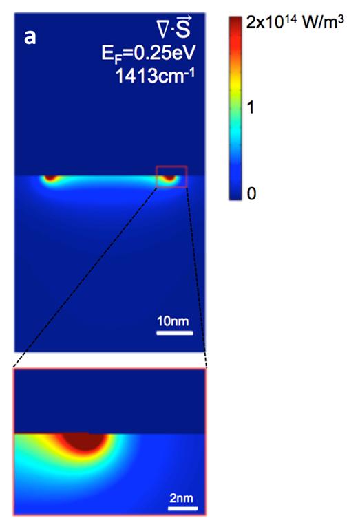
8 on a SiN x /Au substrate at cm -2 carrier density using parameters described in our previous works.[21] The electromagnetic power density models where power is absorbed, and therefore also indicates where far field thermal emission originates. The results of these simulations are shown in Fig. 4(a) at 1413cm -1, corresponding to the graphene plasmon mode. We observe a strong enhancement of the density of electromagnetic power absorption near the graphene resonators. On this resonance, there is a significant amount of power being absorbed into the graphene; however, it can clearly be seen that in the region in which the graphene plasmon extends into the SiN x, there is an enhancement of power absorption, which would translate into an increased rate of spontaneous emission from this part of the substrate. To further quantify this, we integrate the power densities over each material for undoped and doped graphene and see that, the power absorbed into the top 10nm of the SiN x increases with the increased graphene nanoresonator doping as shown in Fig. 4(b). At ~1400cm -1, it is observed that there is weak power absorption in the top layer of SiN x for undoped graphene, and we see only the interband transitions contributing in the graphene itself. Then as the doping is increased to E F =0.25eV, the graphene plasmon can be excited and so absorption in the graphene and top 10nm of SiN x increases due to the effects described above. For comparison we show the absorption features from the remaining bottom 990nm of SiN x. It is important to note that this finite element model does not account for the non-radiative processes discussed above. This model only indicates how graphene plasmons interact with a homogenous, lossy medium and not for the way that localized dipole moments interact with the graphene sheet which is the origin of the nonradiative quenching effects. In order to quantify the thermally radiated power of this structure, we consider Planck s law for spectral radiance using the black soot as a reference with ɛ=1, and including our 50x50 μm 2 collection area and the 1.51 steradians covered by the 0.65 NA objective. We plot these results for different temperatures in Fig. 5, showing an increase in the thermally radiated power that is modulated by the graphene sheet, and a maximum thermal power modulation of 200pW/cm -1 at 1400cm -1 (7.1 μm). These calculations indicate that a 1x1 mm 2 device patterned with 40nm resonators held at 250 C could act as an electronically controllable mid-ir source that would emit 8μW over 100 cm -1 of bandwidth. This compares favorably to commercial mid-ir LEDs at 7μm, which emit 2μW over similar bandwidths.[37] We also note that the maximum temperature and gate bias applied in these experiments was not limited by the graphene but by 8
9 the SiN x dielectric, which is known to exhibit Poole-Frenkel tunneling at high temperatures.[22] By choosing a dielectric that can withstand higher temperatures, such as SiO 2, larger powers could be achieved in such devices. In conclusion, we have demonstrated the direct electronic control of Mid-IR thermal radiation using graphene plasmonic nanoresonators. We show that the graphene plasmonic modes can act to enhace the thermal radiation from the SiN x membrane as well as excitations in the graphene sheet. We have developed a structure with tunable narrowband emission at a range of frequencies in the mid-ir due to graphene nanostructure resonances, and we have shown that this emission can be changed statically with resonator dimensions, and actively with charge carrier density via the application of a gate bias. We estimate that the power emitted from this structure with a 1mm 2 areal coverage could exceed that of mid-ir LEDs. Acknowledgements: This work was supported by the Department of Energy Office of Science, Basic Energy Sciences under Contract No. DE-FG02-07ER46405 (M.C.S.,V.W.B. and H.A.A.). M. S. J. and M. C. acknowledge support from the Global Frontier R&D Program on Center for Multiscale Energy Systems funded by the National Research Foundation under the Ministry of Science, ITC & Future Planning, Korea ( , ). M.C.S. acknowledges support from a Resnick Institute Graduate Fellowship. M.S. J. acknowledges a post-doctoral fellowship from the POSCO TJ Park Foundation. V.W.B. acknowledges support from a Kavli Nanoscience Postdoctoral Fellowship, and use of facilties of the Kavli Nanoscience Institute. Bibliography [1] C. Cornelius and J. Dowling, Physical Review A 59, 4736 (1999). [2] J. Greffet, R. Carminati, K. Joulain, J. Mulet, S. Mainguy, and Y. Chen, Nature 416, 61 (2002). [3] J. A. Schuller, T. Taubner, and M. L. Brongersma, Nature Photonics 3, 658 (2009). [4] X. Liu, T. Tyler, T. Starr, A. F. Starr, N. M. Jokerst, and W. J. Padilla, Physical Review Letters 107 (2011). 9
10 [5] M. A. Kats, R. Blanchard, S. Zhang, P. Genevet, C. Ko, S. Ramanathan, and F. Capasso, Physical Review X 3 (2013). [6] S. M. Rytov, Theory of electric fluctuations and thermal radiation (Electronics Research Directorate, Air Force Cambridge Research Center, Air Research and Development Command, U. S. Air Force, Bedford, Mass.,, 1959). [7] D. Polder and M. Van Hove, Physical Review B 4, 3303 (1971). [8] L. Hu, A. Narayanaswamy, X. Chen, and G. Chen, Applied Physics Letters 92 (2008). [9] E. Rousseau, A. Siria, G. Jourdan, S. Volz, F. Comin, J. Chevrier, and J. J. Greffet, Nat Photon 3, 514 (2009). [10] S. Shen, A. Mavrokefalos, P. Sambegoro, and G. Chen, Applied Physics Letters 100 (2012). [11] C. R. Otey, W. T. Lau, and S. Fan, Physical Review Letters 104, (2010). [12] H. Iizuka and S. Fan, Journal of Applied Physics 112 (2012). [13] R. S. DiMatteo, P. Greiff, S. L. Finberg, K. A. Young Waithe, H. K. H. Choy, M. M. Masaki, and C. G. Fonstad, Applied Physics Letters 79, 1894 (2001). [14] M. D. Whale and E. G. Cravalho, Ieee T Energy Conver 17, 130 (2002). [15] M. Laroche, R. Carminati, and J. J. Greffet, Journal of Applied Physics 100 (2006). [16] A. Narayanaswamy and G. Chen, Applied Physics Letters 82, 3544 (2003). [17] S. Vassant, I. M. Doyen, F. Marquier, F. Pardo, U. Gennser, A. Cavanna, J. L. Pelouard, and J. J. Greffet, Applied Physics Letters 102 (2013). [18] X. Li et al., Science 324, 1312 (2009). [19] X. Li et al., Nano Letters 10, 4328 (2010). [20] K. Novoselov, A. Geim, S. Morozov, D. Jiang, M. Katsnelson, I. Grigorieva, S. Dubonos, and A. Firsov, Nature 438, 197 (2005). [21] M. S. Jang, V. W. Brar, M. Sherrott, J. J. Lopez, L. K. Kim, S. Kim, M. Choi, and H. A. Atwater, arxiv, (2014). [22] A. Dogan, Master of Science, The Pennsylvania State University, [23] V. W. Brar, M. S. Jang, M. Sherrott, J. J. Lopez, and H. A. Atwater, Nano Letters 13, 2541 (2013). [24] M. Jablan, H. Buljan, and M. Soljacic, Physical Review B 80, (2009). [25] A. Principi, G. Vignale, M. Carrega, and M. Polini, Physical Review B 88, (2013). [26] A. Principi, G. Vignale, M. Carrega, and M. Polini, Physical Review B 88, (2013). [27] H. Yan, T. Low, W. Zhu, Y. Wu, M. Freitag, X. Li, F. Guinea, P. Avouris, and F. Xia, Nat Photon 7, 394 (2013). [28] F. Wang, Y. B. Zhang, C. S. Tian, C. Girit, A. Zettl, M. Crommie, and Y. R. Shen, Science 320, 206 (2008). [29] Z. Q. Li, E. A. Henriksen, Z. Jiang, Z. Hao, M. C. Martin, P. Kim, H. L. Stormer, and D. N. Basov, Nat Phys 4, 532 (2008). [30] J. S. Biteen, L. A. Sweatlock, H. Mertens, N. S. Lewis, A. Polman, and H. A. Atwater, Journal of Physical Chemistry C 111, (2007). [31] J. Gersten and A. Nitzan, Journal of Chemical Physics 75, 1139 (1981). [32] J. Kummerlen, A. Leitner, H. Brunner, F. Aussenegg, and A. Wokaun, Molecular Physics 80, 1031 (1993). [33] L. Novotny and N. van Hulst, Nature Photonics 5, 83 (2011). 10
11 [34] F. H. L. Koppens, D. E. Chang, and F. Javier Garcia de Abajo, Nano Letters 11, 3370 (2011). [35] L. Gaudreau, K. J. Tielrooij, G. E. D. K. Prawiroatmodjo, J. Osmond, F. J. G. de Abajo, and F. H. L. Koppens, Nano Letters 13, 2030 (2013). [36] V. W. Brar, M. S. Jang, S. Kim, M. Sherrott, L. K. Kim, J. J. Lopez, M. Choi, and H. A. Atwater, in 2014 MRS Spring Meeting & Exhibit (Materials Research Society, San Francisco, 2014). [37] 11

12 Figures Figure 1: Schematic of experimental setup. (a) Graphene structure on temperature-controlled stage with FTIR emission measurement configuration. Graphene structure consists of μm 2 nanoresonator arrays on a 1μm thick SiN x membrane with 200nm Au backreflector. The graphene was grounded through Au(100nm)/Cr(3nm) electrodes that also served as source-drain contacts. A gate bias was applied through the SiN x membrane between the underlying Si frame and graphene sheet. Temperature controlled stage consists of 100μm thick sapphire on 2mm Cu on an Ag block. Emission measurements were taken at different temperatures via FTIR using a LN 2 cooled MCT detector. (b) A resistance vs gate voltage curve of the graphene sheet showing a peak in the resistance at the charge neutral point (CNP), when the Fermi level (E F ) is aligned with the Dirac point. (c) A representative SEM image of 30nm graphene nanoresonators. 12
13 Figure 2: Normalization scheme adopted for this experiment including reference soot emission spectrum (left axis) taken to have emissivity of unity. Emitted intensity at a given temperature for bare SiN x, graphene at charge neutral point (CNP) and increased carrier density (left axis). Change in emissivity of structure from CNP to doped graphene, normalized to emission spectrum of soot (right axis). Enhancement of emissivity is observed due to increased charge carrier density in graphene. 13
14 Figure 3: Modulation of emissivity and thermal emission. Emissivity calculated using a unity emissivity soot reference at the same temperature. (a) Carrier density dependence of emissivity modulation for a fixed temperature and nanoresonator width. (b) Emissivity modulation for different nanoresonator geometries as well as unpatterned graphene at a fixed temperature and carrier density. (c) Emissivity change for different polarizations of light for a fixed temperature, resonator width, and carrier density. 14
15 15
16 Figure 4: (a) Calculated 2D plot of electromagnetic power density in graphene/sin x structure with vacuum above obtained from finite element electromagnetic simulation. Plotted at 1413cm -1 (graphene plasmon peak) at E F =0.25eV. Enhancement of power density noted closest to graphene surface then decaying into SiN x substrate. (b) Integrated power density in 40nm width graphene resonator, the top 10nm of SiN x (Top SiN x ), and the remaining 990nm of SiN x (Bulk SiN x ) at E F = 0eV and E F = 0.25eV. Figure 5: Thermally radiated power from Graphene/SiN x /Au structure at varying temperatures for a nanoresonator width of 40nm and carrier density of 4.9x10 12 /cm 2. Calculated using black soot reference, based on a 0.65 NA objective and a 50x50μm 2 collection area. A maximum modulation of 200pW/cm -1 is calculated. 16

17 Figure 6: Theoretical change in absorption ( A) as a function of inverse ribbon width at E F =0.25eV. Numerical full-field electromagnetic simulation has been performed using a finite element method under the assumption of normal light incidence. 17
Hybrid Surface-Phonon-Plasmon Polariton Modes in Graphene /
 Supplementary Information: Hybrid Surface-Phonon-Plasmon Polariton Modes in Graphene / Monolayer h-bn stacks Victor W. Brar 1,2, Min Seok Jang 3,, Michelle Sherrott 1, Seyoon Kim 1, Josue J. Lopez 1, Laura
Highly Confined Tunable Mid-Infrared Plasmonics in Graphene Nanoresonators
 Supplementary Information for Highly Confined Tunable Mid-Infrared Plasmonics in Graphene Nanoresonators by Victor W. Brar, Min Seok Jang, Michelle Sherrott, Josue J. Lopez and Harry Atwater 1 Approximating
Electronically Tunable Perfect Absorption in Graphene
 Electronically Tunable Perfect Absorption in Graphene Seyoon Kim 1,, Min Seok Jang 1,2,, Victor W. Brar 1,3,4,, Kelly W. Mauser 1, and Harry A. Atwater 1,3,* * haa@caltech.edu Equally contributed authors
Controlling Graphene Ultrafast Hot Carrier Response from Metal-like. to Semiconductor-like by Electrostatic Gating
 Controlling Graphene Ultrafast Hot Carrier Response from Metal-like to Semiconductor-like by Electrostatic Gating S.-F. Shi, 1,2* T.-T. Tang, 1 B. Zeng, 1 L. Ju, 1 Q. Zhou, 1 A. Zettl, 1,2,3 F. Wang 1,2,3
Nanophotonics: solar and thermal applications
 Nanophotonics: solar and thermal applications Shanhui Fan Ginzton Laboratory and Department of Electrical Engineering Stanford University http://www.stanford.edu/~shanhui Nanophotonic Structures Photonic
Strong coupling in the far-infrared between graphene plasmons and the
 Strong coupling in the far-infrared between graphene plasmons and the surface optical phonons of silicon dioxide I. J. Luxmoore 1,a), C. H. Gan 1, P. Q. Liu 2, F. Valmorra 2, P. Li 1, J. Faist 2, and G.
Monolayer Black Phosphorus
 Supporting Information: Localized Surface Plasmons in Nanostructured Monolayer Black Phosphorus Zizhuo Liu and Koray Aydin* Department of Electrical Engineering and Computer Science, Northwestern University,
Graphene-based long-wave infrared TM surface plasmon modulator
 Graphene-based long-wave infrared TM surface plasmon modulator David R. Andersen 1, 1 Department of Electrical and Computer Engineering, Department of Physics and Astronomy, The University of Iowa, Iowa
Supplementary Information for. Vibrational Spectroscopy at Electrolyte Electrode Interfaces with Graphene Gratings
 Supplementary Information for Vibrational Spectroscopy at Electrolyte Electrode Interfaces with Graphene Gratings Supplementary Figure 1. Simulated from pristine graphene gratings at different Fermi energy
Raman Imaging and Electronic Properties of Graphene
 Raman Imaging and Electronic Properties of Graphene F. Molitor, D. Graf, C. Stampfer, T. Ihn, and K. Ensslin Laboratory for Solid State Physics, ETH Zurich, 8093 Zurich, Switzerland ensslin@phys.ethz.ch
Surface plasmon polaritons (SPPs) are optical modes
 are optical modes") pubs.acs.org/nanolett Highly Confined Tunable Mid-Infrared Plasmonics in Graphene Nanoresonators Victor W. Brar,, Min Seok Jang, Michelle Sherrott, Josue J. Lopez, and Harry A. Atwater*,, Thomas J. Watson
pubs.acs.org/nanolett Highly Confined Tunable Mid-Infrared Plasmonics in Graphene Nanoresonators Victor W. Brar,, Min Seok Jang, Michelle Sherrott, Josue J. Lopez, and Harry A. Atwater*,, Thomas J. Watson
Thin film interference in ultra-thin layers: color coatings, tunable absorbers, and thermal emitters
 Thin film interference in ultra-thin layers: color coatings, tunable absorbers, and thermal emitters Mikhail A. Kats Harvard University School of Engineering and Applied Sciences NanoLight [Benasque] March
Nonlinear Electrodynamics and Optics of Graphene
 Nonlinear Electrodynamics and Optics of Graphene S. A. Mikhailov and N. A. Savostianova University of Augsburg, Institute of Physics, Universitätsstr. 1, 86159 Augsburg, Germany E-mail: sergey.mikhailov@physik.uni-augsburg.de
High temperature plasmonics: Narrowband, tunable, nearfield. thermal sources
 High temperature plasmonics: Narrowband, tunable, nearfield thermal sources Yu Guo, S. Molesky, C. Cortes and Zubin Jacob * Department of Electrical and Computer Engineering, University of Alberta, Edmonton,
Exact microscopic theory of electromagnetic heat transfer
 Exact microscopic theory of electromagnetic heat transfer between a dielectric sphere and plate Clayton Otey 1 and Shanhui Fan 2 1 Department of Applied Physics and 2 Department of Electrical Engineering,
Spatially resolving density-dependent screening around a single charged atom in graphene
 Supplementary Information for Spatially resolving density-dependent screening around a single charged atom in graphene Dillon Wong, Fabiano Corsetti, Yang Wang, Victor W. Brar, Hsin-Zon Tsai, Qiong Wu,
Graphene conductivity mapping by terahertz time-domain reflection spectroscopy
 Graphene conductivity mapping by terahertz time-domain reflection spectroscopy Xiaodong Feng, Min Hu *, Jun Zhou, and Shenggang Liu University of Electronic Science and Technology of China Terahertz Science
Nonlinear optical conductance in a graphene pn junction in the terahertz regime
 University of Wollongong Research Online Faculty of Engineering - Papers (Archive) Faculty of Engineering and Information Sciences 2010 Nonlinear optical conductance in a graphene pn junction in the terahertz
Wednesday 3 September Session 3: Metamaterials Theory (16:15 16:45, Huxley LT308)
") Session 3: Metamaterials Theory (16:15 16:45, Huxley LT308) (invited) TBC Session 3: Metamaterials Theory (16:45 17:00, Huxley LT308) Light trapping states in media with longitudinal electric waves D McArthur,
Session 3: Metamaterials Theory (16:15 16:45, Huxley LT308) (invited) TBC Session 3: Metamaterials Theory (16:45 17:00, Huxley LT308) Light trapping states in media with longitudinal electric waves D McArthur,
Graphene photodetectors with ultra-broadband and high responsivity at room temperature
 SUPPLEMENTARY INFORMATION DOI: 10.1038/NNANO.2014.31 Graphene photodetectors with ultra-broadband and high responsivity at room temperature Chang-Hua Liu 1, You-Chia Chang 2, Ted Norris 1.2* and Zhaohui
PLASMONICS/METAMATERIALS
 PLASMONICS/METAMATERIALS Interconnects Optical processing of data Subwavelength confinement Electrodes are in place Coupling to other on-chip devices Combination of guiding, detection, modulation, sensing
Supporting information. Unidirectional Doubly Enhanced MoS 2 Emission via
 Supporting information Unidirectional Doubly Enhanced MoS 2 Emission via Photonic Fano Resonances Xingwang Zhang, Shinhyuk Choi, Dake Wang, Carl H. Naylor, A. T. Charlie Johnson, and Ertugrul Cubukcu,,*
graphene nano-optoelectronics Frank Koppens ICFO, The institute of photonic sciences, Barcelona
 graphene nano-optoelectronics Frank Koppens ICFO, The institute of photonic sciences, Barcelona Graphene research at ICFO Frank Koppens: group Nano-optoelectronics (~100% graphene) Nano-optics and plasmonics
High-speed waveguide-coupled graphene-on-graphene optical modulators. Steven J. Koester 1 and Mo Li 2
 High-speed waveguide-coupled graphene-on-graphene optical modulators Steven J. Koester 1 and Mo Li 2 Department of Electrical and Computer Engineering, University of Minnesota-Twin Cities, Minneapolis,
Supporting Information for: Gate-Variable Mid-Infrared Optical Transitions in a (Bi 1-
 Supporting Information for: Gate-Variable Mid-Infrared Optical Transitions in a (Bi 1- xsb x ) 2 Te 3 Topological Insulator 1 William S. Whitney, 2,3 Victor W. Brar, 4 Yunbo Ou, 5,6 Yinming Shao, 2 Artur
Near field radiative heat transfer between a sphere and a substrate
 Near field radiative heat transfer between a sphere and a substrate Arvind Narayanaswamy Department of Mechanical Engineering, Columbia University, New York, NY 10027. Sheng Shen and Gang Chen Department
Superconductivity Induced Transparency
 Superconductivity Induced Transparency Coskun Kocabas In this paper I will discuss the effect of the superconducting phase transition on the optical properties of the superconductors. Firstly I will give
Supplementary material for High responsivity mid-infrared graphene detectors with antenna-enhanced photo-carrier generation and collection
 Supplementary material for High responsivity mid-infrared graphene detectors with antenna-enhanced photo-carrier generation and collection Yu Yao 1, Raji Shankar 1, Patrick Rauter 1, Yi Song 2, Jing Kong
Radiative Heat Transfer at the Nanoscale. Pramod Reddy University of Michigan, Ann Arbor
 Radiative Heat Transfer at the Nanoscale 40µm Pramod Reddy University of Michigan, Ann Arbor Acknowledgements Edgar Meyhofer Juan Carlos Cuevas Francisco Garcia Vidal B. Song K. Kim V. Fernandez J. Fiest
Photonics applications II. Ion-doped ChGs
 Photonics applications II Ion-doped ChGs 1 ChG as a host for doping; pros and cons - Important - Condensed summary Low phonon energy; Enabling emission at longer wavelengths Reduced nonradiative multiphonon
Enhancing the Rate of Spontaneous Emission in Active Core-Shell Nanowire Resonators
 Chapter 6 Enhancing the Rate of Spontaneous Emission in Active Core-Shell Nanowire Resonators 6.1 Introduction Researchers have devoted considerable effort to enhancing light emission from semiconductors
Extraordinary Photon Transport by Near-Field Coupling of a Nanostructured Metamaterial with a Graphene-Covered Plate
 Extraordinary Photon Transport by Near-Field Coupling of a Nanostructured Metamaterial with a Graphene-Covered Plate Jui-Yung Chang, Yue Yang, and Liping Wang* School for Engineering of Matter, Transport
Plasmonic Photovoltaics Harry A. Atwater California Institute of Technology
 Plasmonic Photovoltaics Harry A. Atwater California Institute of Technology Surface plasmon polaritons and localized surface plasmons Plasmon propagation and absorption at metal-semiconductor interfaces
Nanoscale optical circuits: controlling light using localized surface plasmon resonances
 Nanoscale optical circuits: controlling light using localized surface plasmon resonances T. J. Davis, D. E. Gómez and K. C. Vernon CSIRO Materials Science and Engineering Localized surface plasmon (LSP)
Graphene-polymer multilayer heterostructure for terahertz metamaterials
 University of Wollongong Research Online Faculty of Engineering and Information Sciences - Papers: Part A Faculty of Engineering and Information Sciences 2013 Graphene-polymer multilayer heterostructure
Ultrafast Lateral Photo-Dember Effect in Graphene. Induced by Nonequilibrium Hot Carrier Dynamics
 1 Ultrafast Lateral Photo-Dember Effect in Graphene Induced by Nonequilibrium Hot Carrier Dynamics Chang-Hua Liu, You-Chia Chang, Seunghyun Lee, Yaozhong Zhang, Yafei Zhang, Theodore B. Norris,*,, and
Supplementary Methods A. Sample fabrication
 Supplementary Methods A. Sample fabrication Supplementary Figure 1(a) shows the SEM photograph of a typical sample, with three suspended graphene resonators in an array. The cross-section schematic is
Tuning optical responses of metallic dipole nanoantenna using graphene
 Tuning optical responses of metallic dipole nanoantenna using graphene Xingang Ren, Wei E. I. Sha, and Wallace C. H. Choy Department of Electrical and Electronic Engineering, The University of Hong Kong,
Active Radiative Thermal Switching with Graphene Plasmon Resonators
 Active Radiative Thermal Switching with Graphene Plasmon Resonators Ognjen Ilic, 1 Nathan H. Thomas, 2 Thomas Christensen, 3 Michelle C. Sherrott, 1 Marin Soljačić, 3 Austin J. Minnich, 2 Owen D. Miller,
Simulated Study of Plasmonic Coupling in Noble Bimetallic Alloy Nanosphere Arrays
 CHAPTER 4 Simulated Study of Plasmonic Coupling in Noble Bimetallic Alloy Nanosphere Arrays 4.1 Introduction In Chapter 3, the noble bimetallic alloy nanosphere (BANS) of Ag 1-x Cu x at a particular composition
(Co-PIs-Mark Brongersma, Yi Cui, Shanhui Fan) Stanford University. GCEP Research Symposium 2013 Stanford, CA October 9, 2013
 Stanford University. GCEP Research Symposium 2013 Stanford, CA October 9, 2013") High-efficiency thin film nano-structured multi-junction solar James S. cells Harris (PI) (Co-PIs-Mark Brongersma, Yi Cui, Shanhui Fan) Stanford University GCEP Research Symposium 2013 Stanford, CA October
High-efficiency thin film nano-structured multi-junction solar James S. cells Harris (PI) (Co-PIs-Mark Brongersma, Yi Cui, Shanhui Fan) Stanford University GCEP Research Symposium 2013 Stanford, CA October
Scattering-type near-field microscopy for nanoscale optical imaging
 Scattering-type near-field microscopy for nanoscale optical imaging Rainer Hillenbrand Nano-Photonics Group Max-Planck-Institut für Biochemie 82152 Martinsried, Germany Infrared light enables label-free
Black phosphorus: A new bandgap tuning knob
 Black phosphorus: A new bandgap tuning knob Rafael Roldán and Andres Castellanos-Gomez Modern electronics rely on devices whose functionality can be adjusted by the end-user with an external knob. A new
Chapter 3 Properties of Nanostructures
 Chapter 3 Properties of Nanostructures In Chapter 2, the reduction of the extent of a solid in one or more dimensions was shown to lead to a dramatic alteration of the overall behavior of the solids. Generally,
Electronic and Optoelectronic Properties of Semiconductor Structures
 Electronic and Optoelectronic Properties of Semiconductor Structures Jasprit Singh University of Michigan, Ann Arbor CAMBRIDGE UNIVERSITY PRESS CONTENTS PREFACE INTRODUCTION xiii xiv 1.1 SURVEY OF ADVANCES
Graphene Plasmon Enhanced Vibrational Sensing of Surface- Adsorbed Layers
 pubs.acs.org/nanolett Graphene Plasmon Enhanced Vibrational Sensing of Surface- Adsorbed Layers Yilei Li,, Hugen Yan, Damon B. Farmer, Xiang Meng,, Wenjuan Zhu, Richard M. Osgood,, Tony F. Heinz,, and
Nonlinear optics with quantum-engineered intersubband metamaterials
 Nonlinear optics with quantum-engineered intersubband metamaterials Mikhail Belkin Department of Electrical and Computer Engineering The University of Texas at Austin 1 Mid-infrared and THz photonics Electronics
Understanding Nanoplasmonics. Greg Sun University of Massachusetts Boston
 Understanding Nanoplasmonics Greg Sun University of Massachusetts Boston Nanoplasmonics Space 100pm 1nm 10nm 100nm 1μm 10μm 100μm 1ns 100ps 10ps Photonics 1ps 100fs 10fs 1fs Time Surface Plasmons Surface
Figure 1 Relaxation processes within an excited state or the ground state.
 Excited State Processes and Application to Lasers The technology of the laser (Light Amplified by Stimulated Emission of Radiation) was developed in the early 1960s. The technology is based on an understanding
The Dielectric Function of a Metal ( Jellium )
") The Dielectric Function of a Metal ( Jellium ) Total reflection Plasma frequency p (10 15 Hz range) Why are Metals Shiny? An electric field cannot exist inside a metal, because metal electrons follow the
The Dielectric Function of a Metal ( Jellium ) Total reflection Plasma frequency p (10 15 Hz range) Why are Metals Shiny? An electric field cannot exist inside a metal, because metal electrons follow the
Optimizing the performance of metal-semiconductor-metal photodetectors by embedding nanoparticles in the absorption layer
 Journal of Electrical and Electronic Engineering 2015; 3(2-1): 78-82 Published online February 10, 2015 (http://www.sciencepublishinggroup.com/j/jeee) doi: 10.11648/j.jeee.s.2015030201.27 ISSN: 2329-1613
A Study on the Suitability of Indium Nitride for Terahertz Plasmonics
 A Study on the Suitability of Indium Nitride for Terahertz Plasmonics Arjun Shetty 1*, K. J. Vinoy 1, S. B. Krupanidhi 2 1 Electrical Communication Engineering, Indian Institute of Science, Bangalore,
Highly Sensitive and Wide-Band Tunable Terahertz Response of Plasma Wave based on Graphene Field Effect Transistors
 Supplementary Information Highly Sensitive and Wide-Band Tunable Terahertz Response of Plasma Wave based on Graphene Field Effect Transistors Lin Wang, Xiaoshuang Chen *, Anqi Yu, Yang Zhang, Jiayi Ding
Chapter-4 Stimulated emission devices LASERS
 Semiconductor Laser Diodes Chapter-4 Stimulated emission devices LASERS The Road Ahead Lasers Basic Principles Applications Gas Lasers Semiconductor Lasers Semiconductor Lasers in Optical Networks Improvement
Magneto-Optical Cavity-Type Resonators as Controllable Narrow-Band Sources of Infrared Radiation
 American Journal of Modern Physics and Application 8; 5(4): 77-8 http://www.openscienceonline.com/journal/ajmpa Magneto-Optical Cavity-Type Resonators as Controllable Narrow-Band Sources of Infrared Radiation
UvA-DARE (Digital Academic Repository) Charge carrier dynamics in photovoltaic materials Jensen, S.A. Link to publication
 Charge carrier dynamics in photovoltaic materials Jensen, S.A. Link to publication") UvA-DARE (Digital Academic Repository) Charge carrier dynamics in photovoltaic materials Jensen, S.A. Link to publication Citation for published version (APA): Jensen, S. A. (2014). Charge carrier dynamics
UvA-DARE (Digital Academic Repository) Charge carrier dynamics in photovoltaic materials Jensen, S.A. Link to publication Citation for published version (APA): Jensen, S. A. (2014). Charge carrier dynamics
Photonic thermal diode enabled by surface polariton coupling in. nanostructures
 Photonic thermal diode enabled by surface polariton coupling in nanostructures Lei Tang and Mathieu Francoeur * Radiative Energy Transfer Lab, Department of Mechanical Engineering, University of Utah,
Circularly polarized thermal emission from chiral metasurface in the absence of magnetic field
 Journal of Physics: Conference Series PAPER OPEN ACCESS Circularly polarized thermal emission from chiral metasurface in the absence of magnetic field To cite this article: S.A. Dyakov et al 2018 J. Phys.:
Optical nano-imaging of gate-tuneable graphene plasmons
 Optical nano-imaging of gate-tuneable graphene plasmons Jianing Chen *,5,1, Michela Badioli *,2, Pablo Alonso-González *1, Suko Thongrattanasiri *,3, Florian Huth *1,6, Johann Osmond 2, Marko Spasenović
requency generation spectroscopy Rahul N
 requency generation spectroscopy Rahul N 2-11-2013 Sum frequency generation spectroscopy Sum frequency generation spectroscopy (SFG) is a technique used to analyze surfaces and interfaces. SFG was first
Graphene Canada Montreal Oct. 16, 2015 (International Year of Light)
") Luminescence Properties of Graphene A. Beltaos 1,2,3, A. Bergren 1, K. Bosnick 1, N. Pekas 1, A. Matković 4, A. Meldrum 2 1 National Institute for Nanotechnology (NINT), 11421 Saskatchewan Drive, Edmonton,
Luminescence Properties of Graphene A. Beltaos 1,2,3, A. Bergren 1, K. Bosnick 1, N. Pekas 1, A. Matković 4, A. Meldrum 2 1 National Institute for Nanotechnology (NINT), 11421 Saskatchewan Drive, Edmonton,
Supplementary Figure S1. AFM images of GraNRs grown with standard growth process. Each of these pictures show GraNRs prepared independently,
 Supplementary Figure S1. AFM images of GraNRs grown with standard growth process. Each of these pictures show GraNRs prepared independently, suggesting that the results is reproducible. Supplementary Figure
Temperature Dependent Optical Band Gap Measurements of III-V films by Low Temperature Photoluminescence Spectroscopy
 Temperature Dependent Optical Band Gap Measurements of III-V films by Low Temperature Photoluminescence Spectroscopy Linda M. Casson, Francis Ndi and Eric Teboul HORIBA Scientific, 3880 Park Avenue, Edison,
Chemistry Instrumental Analysis Lecture 5. Chem 4631
 Chemistry 4631 Instrumental Analysis Lecture 5 Light Amplification by Stimulated Emission of Radiation High Intensities Narrow Bandwidths Coherent Outputs Applications CD/DVD Readers Fiber Optics Spectroscopy
Multi-cycle THz pulse generation in poled lithium niobate crystals
 Laser Focus World April 2005 issue (pp. 67-72). Multi-cycle THz pulse generation in poled lithium niobate crystals Yun-Shik Lee and Theodore B. Norris Yun-Shik Lee is an assistant professor of physics
Nanophysics: Main trends
 Nano-opto-electronics Nanophysics: Main trends Nanomechanics Main issues Light interaction with small structures Molecules Nanoparticles (semiconductor and metallic) Microparticles Photonic crystals Nanoplasmonics
Supporting Information. by Hexagonal Boron Nitride
 Supporting Information High Velocity Saturation in Graphene Encapsulated by Hexagonal Boron Nitride Megan A. Yamoah 1,2,, Wenmin Yang 1,3, Eric Pop 4,5,6, David Goldhaber-Gordon 1 * 1 Department of Physics,
Introduction to Sources: Radiative Processes and Population Inversion in Atoms, Molecules, and Semiconductors Atoms and Molecules
 OPTI 500 DEF, Spring 2012, Lecture 2 Introduction to Sources: Radiative Processes and Population Inversion in Atoms, Molecules, and Semiconductors Atoms and Molecules Energy Levels Every atom or molecule
photonic crystals School of Space Science and Physics, Shandong University at Weihai, Weihai , China
 Enhanced absorption in heterostructures with graphene and truncated photonic crystals Yiping Liu 1, Lei Du 1, Yunyun Dai 2, Yuyu Xia 2, Guiqiang Du 1,* Guang Lu 1, Fen Liu 1, Lei Shi 2, Jian Zi 2 1 School
Bends and splitters in graphene nanoribbon waveguides
 Downloaded from orbit.dtu.dk on: Dec 20, 2017 Bends and splitters in graphene nanoribbon waveguides Zhu, Xiaolong; Yan, Wei; Mortensen, N. Asger; Xiao, Sanshui Published in: Optics Express Link to article,
arrays for mid-infrared plasmonics
 Scalable and tunable periodic graphene nano-hole arrays for mid-infrared plasmonics Kavitha K. Gopalan*, Bruno Paulillo*, David M.A. Mackenzie +, Daniel Rodrigo*, Nestor Bareza*, Patrick R. Whelan +, Abhay
Chapter 2 Optical Transitions
 Chapter 2 Optical Transitions 2.1 Introduction Among energy states, the state with the lowest energy is most stable. Therefore, the electrons in semiconductors tend to stay in low energy states. If they
SENSITIVITY ENHANCEMENT OF A D-SHAPE SPR-POF LOW-COST SENSOR USING GRAPHENE
 International Journal of Education and Research Vol. No. November 03 SENSITIVITY ENHANCEMENT OF A D-SHAPE SPR-POF LOW-COST SENSOR USING GRAPHENE Ramona GALATUS, Lorant SZOLGA, Emil VOICULESCU Technical
Radiation-matter interaction.
 Radiation-matter interaction Radiation-matter interaction Classical dipoles Dipole radiation Power radiated by a classical dipole in an inhomogeneous environment The local density of optical states (LDOS)
Supplementary Figure S1 SEM and optical images of Si 0.6 H 0.4 colloids. a, SEM image of Si 0.6 H 0.4 colloids. b, The size distribution of Si 0.
 Supplementary Figure S1 SEM and optical images of Si 0.6 H 0.4 colloids. a, SEM image of Si 0.6 H 0.4 colloids. b, The size distribution of Si 0.6 H 0.4 colloids. The standard derivation is 4.4 %. Supplementary
Acoustic metamaterials in nanoscale
 Acoustic metamaterials in nanoscale Dr. Ari Salmi www.helsinki.fi/yliopisto 12.2.2014 1 Revisit to resonances Matemaattis-luonnontieteellinen tiedekunta / Henkilön nimi / Esityksen nimi www.helsinki.fi/yliopisto
Answers to questions on exam in laser-based combustion diagnostics on March 10, 2006
 Answers to questions on exam in laser-based combustion diagnostics on March 10, 2006 1. Examples of advantages and disadvantages with laser-based combustion diagnostic techniques: + Nonintrusive + High
THz QCL sources based on intracavity difference-frequency mixing
 THz QCL sources based on intracavity difference-frequency mixing Mikhail Belkin Department of Electrical and Computer Engineering The University of Texas at Austin IQCLSW, Sept. 3, 218 Problems with traditional
Carbon Nanomaterials
 Carbon Nanomaterials STM Image 7 nm AFM Image Fullerenes C 60 was established by mass spectrographic analysis by Kroto and Smalley in 1985 C 60 is called a buckminsterfullerene or buckyball due to resemblance
2. The electrochemical potential and Schottky barrier height should be quantified in the schematic of Figure 1.
 Reviewers' comments: Reviewer #1 (Remarks to the Author): The paper reports a photon enhanced thermionic effect (termed the photo thermionic effect) in graphene WSe2 graphene heterostructures. The work
Terahertz Lasers Based on Intersubband Transitions
 Terahertz Lasers Based on Intersubband Transitions Personnel B. Williams, H. Callebaut, S. Kumar, and Q. Hu, in collaboration with J. Reno Sponsorship NSF, ARO, AFOSR,and NASA Semiconductor quantum wells
Diode Lasers and Photonic Integrated Circuits
 Diode Lasers and Photonic Integrated Circuits L. A. COLDREN S. W. CORZINE University of California Santa Barbara, California A WILEY-INTERSCIENCE PUBLICATION JOHN WILEY & SONS, INC. NEW YORK / CHICHESTER
Intrinsic Electronic Transport Properties of High. Information
 Intrinsic Electronic Transport Properties of High Quality and MoS 2 : Supporting Information Britton W. H. Baugher, Hugh O. H. Churchill, Yafang Yang, and Pablo Jarillo-Herrero Department of Physics, Massachusetts
Thermal Emission in the Near Field from Polar Semiconductors and the Prospects for Energy Conversion
 Thermal Emission in the Near Field from Polar Semiconductors and the Prospects for Energy Conversion R.J. Trew, K.W. Kim, V. Sokolov, and B.D Kong Electrical and Computer Engineering North Carolina State
Fourier Optics on Graphene
 Fourier Optics on Graphene Ashkan Vakil and Nader Engheta * Department of Electrical & Systems Engineering University of Pennsylvania Philadelphia, PA 19104, USA Abstract Using numerical simulations, here
Biosensing based on slow plasmon nanocavities
 iosensing based on slow plasmon nanocavities. Sepulveda, 1, Y. Alaverdyan,. rian, M. Käll 1 Nanobiosensors and Molecular Nanobiophysics Group Research Center on Nanoscience and Nanotechnolog (CIN)CSIC-ICN
Aluminum for nonlinear plasmonics: Methods Section
 Aluminum for nonlinear plasmonics: Methods Section Marta Castro-Lopez, Daan Brinks, Riccardo Sapienza, and Niek F. van Hulst, ICFO - Institut de Ciencies Fotoniques, and ICREA - Institució Catalana de
Dynamically-Tunable Terahertz Band-Stop Filter Based on Multilayer Graphene Metamaterial
 International Journal of Optics and Applications 27, 7(): 7-2 DOI: 923/j.optics.277.2 Dynamically-Tunable Terahertz Band-Stop Filter Based on Multilayer Graphene Metamaterial Ali Akhavan, Hassan Ghafoori
Supplementary Figure 1 Magneto-transmission spectra of graphene/h-bn sample 2 and Landau level transition energies of three other samples.
 Supplementary Figure 1 Magneto-transmission spectra of graphene/h-bn sample 2 and Landau level transition energies of three other samples. (a,b) Magneto-transmission ratio spectra T(B)/T(B 0 ) of graphene/h-bn
Highly tunable hybrid metamaterials employing split-ring resonators
 Highly tunable hybrid metamaterials employing split-ring resonators strongly coupled to graphene surface plasmons Peter Q. Liu, 1 * Isaac J. Luxmoore, 2 * Sergey A. Mikhailov, 3 Nadja A. Savostianova,
NSF EPSCoR Kansas Center for Solar Energy Research Annual Program Review June 12-14, 2011
 NSF EPSCoR Kansas Center for Solar Energy Research Annual Program Review June 12-14, 2011 Plasmonic and Photonic Photovoltaics based on graphene and other carbon nanostructures Fengli Wang, Guowei Xu,
Shaping the Beam of Light in Nanometer Scales: A Yagi-Uda Nanoantenna in Optical Domain
 Shaping the Beam of Light in Nanometer Scales: A Yagi-Uda Nanoantenna in Optical Domain Jingjing Li, Alessandro Salandrino, and Nader Engheta* University of Pennsylvania Department of Electrical and Systems
Control of thermal radiation for energy applications. Shanhui Fan Ginzton Laboratory and Department of Electrical Engineering Stanford University
 Control of thermal radiation for energy applications Shanhui Fan Ginzton Laboratory and Department of Electrical Engineering Stanford University Thermal radiation: an ubiquitous aspect of nature Sun (6000K)
Supplementary Figure 1. Selected area electron diffraction (SAED) of bilayer graphene and tblg. (a) AB
 of bilayer graphene and tblg. (a) AB") Supplementary Figure 1. Selected area electron diffraction (SAED) of bilayer graphene and tblg. (a) AB stacked bilayer graphene (b), (c), (d), (e), and (f) are twisted bilayer graphene with twist angle
Supplementary Figure 1. Selected area electron diffraction (SAED) of bilayer graphene and tblg. (a) AB stacked bilayer graphene (b), (c), (d), (e), and (f) are twisted bilayer graphene with twist angle
Analytical Spectroscopy Review
 Analytical Spectroscopy Review λ = wavelength ν = frequency V = velocity = ν x λ = 2.998 x 10 8 m/sec = c (in a vacuum) ν is determined by source and does not change as wave propogates, but V can change
Coupling-Enhanced Broadband Mid-Infrared Light Absorption in Graphene Plasmonic Nanostructures
 Coupling-Enhanced Broadband Mid-Infrared Light Absorption in Graphene Plasmonic Nanostructures Bingchen Deng, Qiushi Guo, Cheng Li, Haozhe Wang, Xi Ling, Damon B. Farmer, Shu-jen Han, Jing Kong, and Fengnian
Tunneling characteristics of graphene
 Tunneling characteristics of graphene Young Jun Shin, 1,2 Gopinadhan Kalon, 1,2 Jaesung Son, 1 Jae Hyun Kwon, 1,2 Jing Niu, 1 Charanjit S. Bhatia, 1 Gengchiau Liang, 1 and Hyunsoo Yang 1,2,a) 1 Department
Nanoscale Heat Transfer and Information Technology
 Response to K.E. Goodson Nanoscale Heat Transfer and Information Technology Gang Chen Mechanical Engineering Department Massachusetts Institute of Technology Cambridge, MA 02139 Rohsenow Symposium on Future
Supplementary Information
 Electronic Supplementary Material (ESI) for Physical Chemistry Chemical Physics. This journal is the Owner Societies 2015 Supplementary Information Vertical Heterostructures of MoS2 and Graphene Nanoribbons
Surface plasmon modes in graphene wedge and groove waveguides
 Surface plasmon modes in graphene wedge and groove waveguides Penghong Liu, 1,2 Xinzheng Zhang, 1,2 Zenghong Ma, 1,2 Wei Cai, 1,2, Lei Wang, 1,2 and Jingjun Xu 1,2,3 1 The Key Laboratory of Weak-Light