Highly tunable hybrid metamaterials employing split-ring resonators
|
|
|
- Noreen Gibbs
- 5 years ago
- Views:
Transcription
1 Highly tunable hybrid metamaterials employing split-ring resonators strongly coupled to graphene surface plasmons Peter Q. Liu, 1 * Isaac J. Luxmoore, 2 * Sergey A. Mikhailov, 3 Nadja A. Savostianova, 3 Federico Valmorra, 1 Jerome Faist, 1 Geoffrey R. Nash 2 1 Institute for Quantum Electronics, Department of Physics, ETH Zurich, Zurich CH-8093, Switzerland 2 College of Engineering, Mathematics and Physical Sciences, University of Exeter, Exeter EX4 4QF, United Kingdom 3 Institute of Physics, University of Augsburg, Augsburg 86159, Germany These authors contributed equally to the work. *To whom correspondence should be addressed. qliu@ethz.ch; i.j.luxmoore@exeter.ac.uk 1
2 Abstract Metamaterials and plasmonics are powerful tools for unconventional manipulation and harnessing of light. Metamaterials can be engineered to possess intriguing properties lacking in natural materials, such as negative refractive index. Plasmonics offers capabilities to confine light in subwavelength dimensions and to enhance light-matter interactions. Recently, graphene-based plasmonics has revealed emerging technological potential as it features large tunability, higher field-confinement and lower loss compared to metal-based plasmonics. Here, we introduce hybrid structures comprising graphene plasmonic resonators efficiently coupled to conventional split-ring resonators, thus demonstrating a type of highly tunable metamaterial, where the interaction between the two resonances reaches the strong-coupling regime. Such hybrid metamaterials are employed as high-speed THz modulators, exhibiting over 60% transmission modulation and operating speed in excess of 40 MHz. This device concept also provides a platform for exploring cavity-enhanced light-matter interactions and optical processes in graphene plasmonic structures for applications including sensing, photo-detection and nonlinear frequency generation. Since the turn of the century, research on metamaterials has progressed rapidly with substantial expansion of both the scope of novel functionalities and the operating frequency range enabled by different types of artificial structures Many of the demonstrated metamaterials are based on noble metals to take advantage of their negative permittivity below the plasma frequency. Real-time tunability of metamaterials is highly desired for many applications such as optical switches and modulators, however, it is a property lacking in metals. Different approaches have been developed to achieve tunable or reconfigurable metamaterials, among which several most effective realizations are based on changing the substrate properties Such approaches may find limitations where the properties of the substrate material cannot or should not be changed significantly, and metamaterial structures with intrinsic tunability are keenly sought after. Graphene, a more recently discovered 2
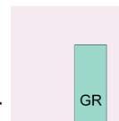
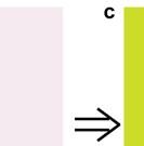
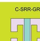
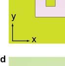
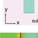
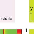
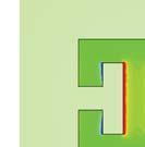
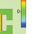
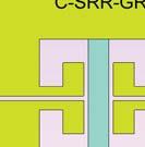
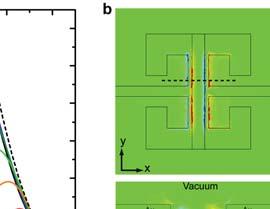
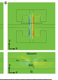
3 and intensively studied material with various interesting properties such as its tunable carrier density and high room-temperature carrier mobility, is a promising candidate for realizing tunable metamaterials across a broad spectral range 18. Graphene s capability to support tightly confined surface plasmon (SP) in the terahertz (THz) to mid-infrared (MIR) spectral range 19,20 has been systematically investigated using scanning near-field optical microscopy and demonstrated in various patterned graphene structures 26-33, including arrays of closely packed graphene ribbons (GR), which are essentially tunable metamaterials. However, the limited interaction between incident light and SP in monolayer graphene structures is not sufficient for many applications. Here, we demonstrate as proof-of-concept a type of electrostatically tunable hybrid metamaterial employing graphene plasmonic resonators strongly coupled to conventional metal-based metamaterials. In addition to their strong electromagnetic response and high tunability, such hybrid metamaterials also provide an interesting platform for exploring cavity-enhanced optical processes and light-matter interactions in graphene plasmonic structures for applications including sensing 34, photo-detection 35,36 and nonlinear frequency generation 37. The proposed hybrid metamaterial concept can be applied to different types of structures, but in this work the specific realization is based on GRs and electric-field-coupled complementary split-ring resonators (C-SRRs) 38,39. The schematics of a C-SRR unit cell, a GR and a unit cell of the proposed hybrid structure are illustrated in Fig. 1a-c. The rationale for such a hybrid structure design is the following: the near-field electric field (E-field) distribution associated with the LC-resonance of the C-SRR is highly localized and enhanced within the capacitor gap as shown by the simulation in Fig. 1d (see Methods), while the E-field distribution of the GR localized SP resonance is also highly confined in the vicinity of the GR (Fig. 1e). Both resonances are excited by E-field in the x- direction 26,38, and upon excitation their highly confined near-field also has the strongest E-field component in the x-direction. Therefore, embedding the GR in the middle of the C-SRR capacitor gap is an effective way to achieve strong near-field coupling of the two structures. When the localized SP resonance of the GR is tuned to approach and subsequently surpass the C-SRR LC-resonance by electrostatically varying the carrier density ( / E F / ), the spectral response of the 3
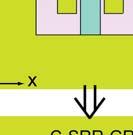
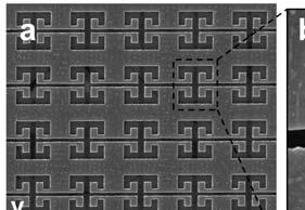
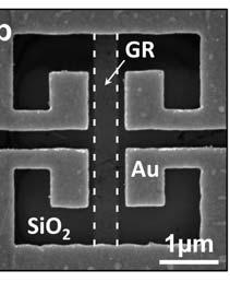
4 hybrid metamaterial is modulated in the frequency range containing the two resonances. Such a mechanism of transmission modulation is significantly different from those employing tunable substrate free carrier absorption 12,13. Due to the confined dimension along the GR width, the Drudetype free carrier absorption is considerably suppressed when the incident radiation is polarized perpendicular to the GR, and the localized SP resonance is the dominant process 26. In order to achieve large modulation, the C-SRR capacitor gap should be designed to accommodate the GR with small margins to maximize the field overlap and hence the coupling strength. In addition, precise control of the hybrid metamaterial spectral response requires accurate information on the charge neutrality point (CNP) of the GRs. Therefore, a modified unit cell design is developed (Fig. 1f) in which a narrow gap along the horizontal symmetry axis is introduced to separate the C-SRR into two parts with minimal influence on its spectral response and field distribution (see Supplementary Information). This slight structural variation allows for convenient electrical characterization of the GR with the two C-SRR parts functioning as separate contacts, and may also enable direct probing of the GR photoresponse 35,36 as influenced by the C-SRR cavity. Following the above design principle, we have developed and experimentally investigated multiple different hybrid metamaterial structures targeting two different operating frequency ranges, i.e. ~10 THz and ~4.5 THz. To achieve this, GR widths of ~400 nm and ~1.8 m, respectively, are chosen to ensure that the SP resonance can be electrostatically tuned across the C-SRR LC resonance 31, even when moderate screening effect from the metal is present (see Supplementary Information). The GRs are implemented with large-area monolayer graphene grown by chemical vapor deposition (CVD) and transferred onto a SiO 2 /Si substrate, which is also utilized as the back-gate for electrostatic control of the graphene carrier density. Electron-beam lithography is employed for patterning the structures (see Methods). Figure 2 shows scanning electron microscope (SEM) images of a fabricated C-SRR-GR array designed to operate around 10 THz. To investigate the carrier density dependent spectral response of the fabricated C-SRR-GR hybrid metamaterial devices, their transmission spectra are characterized employing Fourier transform spectroscopy (FTIR) with the normally incident radiation polarized perpendicular to the GRs (see 4
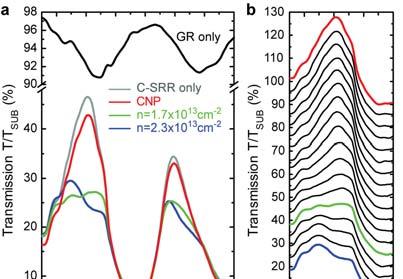
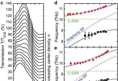
5 Methods). Figure 3 summarizes the key results from two hybrid metamaterial devices (HM1 and HM2) designed to operate around 10 THz. The two devices employ GRs of identical width (400 nm), while the C-SRR unit cell of HM2 is scaled up in-plane by 10% compared to that of HM1 to attain a slightly lower (by ~10%) LC-resonance frequency. Figure 3a shows the transmission spectra of HM1 at 3 different carrier densities in comparison with that of a reference bare C-SRR array. The bare C-SRR array exhibits two resonances in the measured frequency range. The resonance at ~10 THz corresponds to the designed LC-resonance, whereas the resonance at ~16 THz is attributed to the complementary of the half-wave dipole antenna associated with the vertical dimension of the original SRR 12. Figure 3a also shows the transmission spectrum of an array of 400-nm-wide GRs with a carrier density of cm -2, in which two resonances originating from the strong coupling of the intrinsic graphene SP resonance to an optical phonon mode of the underlying SiO 2 layer are present 31 (see Supplementary Information). Both the C-SRR LC-resonance and the GR SP resonance at ~10 THz have a quality factor larger than 3, the latter of which also benefits from the coupling to the SiO 2 phonon. Although the higher-frequency graphene SP resonance interacts with the higher-frequency C- SRR resonance, their coupling strength is expected to be weak due to the large spatial extent of the half-wave dipole antenna mode, and therefore is not the focus of this study. Focusing on the spectral range near the LC-resonance, it is evident that at the CNP, the transmission spectrum of the device is close to that of the corresponding reference C-SRR array, whereas large transmission modulation in both amplitude and line shape is realized by varying the carrier density, with up to ~50% relative modulation of the peak transmission achieved with HM1. This is in sharp contrast to previous investigations where a continuous layer of graphene is brought into contact with SRRs 40,41 and the LC-resonance of the SRRs is considerably diminished even at the CNP condition 41. Moreover, the transmission spectra at high carrier densities display a double-peak feature. This is a characteristic feature of the strong coupling 42,43 between the C-SRR LC-resonance and the GR localized SP resonance due to efficient near-field interaction, which leads to two hybridized modes, i.e. polaritons. The evolution of the transmission of HM1 with increasing carrier density is more clearly revealed in Fig. 3b, in which the higher-frequency peak is observed to gradually blue-shift 5
6 with decreasing strength, while the lower-frequency peak emerges and becomes more pronounced at higher carrier densities. Similar behavior is also observed in HM2 (Fig. 3c) with a noteworthy difference that the lower-frequency peak becomes more dominant at the highest achieved carrier densities. This is consistent with the fact that the LC-resonance frequency is lower in HM2 which allows the SP resonance to surpass the LC-resonance by a larger amount. The frequencies of the individual peaks in the transmission spectra are extracted by fitting the data with two Lorentzian functions, and the results are plotted in Fig. 3d for HM1 and Fig. 3e for HM2. The evolution of the upper and the lower polariton branches with the SP resonance frequency are well fitted with a formula ± = ± + (1) describing the anti-crossing behavior of two strongly coupled resonances 44, where is a parameter determining the coupling strength, and may also be interpreted with an equivalent circuit model as the relative strength of a capacitive coupling between two LC-resonators (see Supplementary Information). The splitting between the two branches ( ) when = is approximately, and the coupling strength (half of this splitting) is found to be ~1.1 THz in both devices, more than 10% of the individual resonance frequency and is therefore also within the ultra-strong coupling regime 45. These experimental observations are well reproduced by full-wave simulations. Figure 4a shows the simulated transmission spectra of HM1 at various carrier densities in comparison with that of a bare C-SRR array. Both the large transmission modulation and the double-peak profile at high carrier densities are consistent with the experimental observations. The simulated E-field profiles associated with the two transmission peaks at E F =0.4 ev (Fig. 4b-c) evidently reveal that the lower-frequency peak stems from a bonding mode, and the higher-frequency peak an anti-bonding mode 46. The two hybridized modes exhibit a typical anti-crossing behavior (Fig. 4d) as well as exchange of their oscillator strengths, as the localized SP resonance approaches and subsequently surpasses the LCresonance with increasing carrier density. The coupling strength is extracted to be ~1.15 THz (see Supplementary Information), in excellent agreement with the experimental result (~1.1 THz). The 6
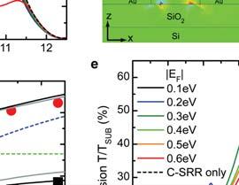
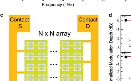
7 field localization and enhancement near the GR in the hybrid structure is also considerably increased compared to either the bare C-SRR or the bare GR (the field enhancement near the GR edges is ~8 times higher when the C-SRR is present), which leads to enhanced absorption of incident radiation and may find applications in chemical and biological sensing. Furthermore, with graphene of higher material quality and thus higher carrier mobility, the carrier density dependent modulation of the transmission is expected to be further improved. As shown in the simulated spectra in Fig. 4e assuming a carrier mobility that is realistic for the state-of-the-art CVD grown graphene 47,48, the transmission of such a hybrid metamaterial can be switched almost completely off across a wide frequency range by controlling the graphene carrier density. Such a superior modulation performance is a direct consequence of the strong coupling between the two resonances. The demonstrated C-SRR-GR hybrid metamaterials can be utilized as efficient modulators and switches. Since fast modulation is highly desired for many applications such as real-time compressive imaging 11,49 and wireless communication, the modulation speed of several devices operating around 4.5 THz are investigated using a THz quantum cascade laser (4.7 THz) as the source. Figure 5a-b show the transmission spectra of two hybrid metamaterial structures (HM3 and HM4) operating at ~4.0 THz and ~4.8 THz, respectively, at various back-gate voltages in comparison with the transmission spectrum of the corresponding reference bare C-SRR array. The transmission exhibits similar (even higher) carrier density dependent modulation as observed in the 10 THz devices, with over 60% relative modulation of the peak transmission. The plateau-shaped transmission spectra in both figures correspond to the situation where the two hybridized modes have similar strengths, and they also suggest that the two resonances are in the critical coupling regime, i.e., the coupling strength is close to half of the broadening, and thus the individual transmission peaks associated with each polariton mode are not as clearly resolved as in the 10 THz devices, consistent with the simulation (see Supplementary Information). This is a result of the relatively lower quality factor of both the GR SP resonance and the C-SRR LC-resonance in this frequency range (Q~2). The C-SRR-GR structure allows for straightforward parallel electrical connection of all the unit cells, as illustrated in Fig. 5c, to minimize the total resistance of the device. Hence, as the total capacitance (C) increases proportional 7
8 to the device area, the total resistance (R) associated with the entire C-SRR-GR array scales inversely proportional to the device area, facilitating high-speed operation of large-area devices. Figure 5d shows the modulation speed measurement (see Methods) of a HM3 device (1 mm 1 mm area) and a HM4 device (0.5 mm 0.5 mm area), respectively. The measured 3 db cut-off frequency is ~19 MHz for the larger device and ~41 MHz for the smaller device. To the best of our knowledge, such performance is superior to the state-of-the-art for fast tunable metamaterials in the literature which was achieved with much smaller device area 50, and is several times higher than that reported for devices with similar area 49. Electrical characterizations show that the resistance of the C-SRR-GR array is indeed not the limiting factor for the RC constant of these devices, whereas the dominant resistance contribution is from the low-doped Si substrate (due to the in-plane current flow) and the input resistance (50 ) of the driving voltage source (see Supplementary Information). The modulation speed can be further enhanced up to GHz range without the need of reducing the device area. For example, by utilizing a wire-grid contact on the backside of the Si substrate, the substrate contribution to the total resistance can be reduced by more than one order of magnitude without affecting the transmission of THz radiation. The total capacitance can also be significantly reduced with further optimization of the device architecture, such as employing a transparent local top-gate for only the GRs or using resonator structures covering less area. The demonstrated concept of coupling graphene-based plasmonic structures with conventional metalbased metamaterials to achieve highly tunable hybrid metamaterials can be straightforwardly extended to other frequency ranges (e.g. MIR) and different graphene plasmonic and/or metameterial structures (e.g. graphene disks and negative-index metamaterials), to further broaden the scope of novel functionalities. The presented device structures also provide a platform for further exploring intriguing cavity-enhanced light-matter interactions and optical processes in graphene plasmonic structures which may lead to various additional applications such as sensing, photo-detection and nonlinear frequency generation. 8
9 Methods Device fabrication. The C-SRR-GR hybrid metamaterials are fabricated from pre-transferred largearea CVD grown monolayer graphene on 300 nm thick SiO 2, which has an underlying Si substrate with resistivity of ~10 cm. Electron-beam lithography and reactive ion etching with O 2 plasma are used to pattern the continuous graphene sheet into arrays of ribbons with the designed widths and separations. A second stage of electron-beam lithography followed by deposition of Cr/Au (thickness 5/80 nm) and a lift-off process defines the C-SRR arrays, which are in direct contact with the GRs to enable electrostatic control of the carrier density using the Si substrate as the back-gate, as well as direct characterization of the electrical properties of the GRs. The devices operating around 10 THz have a surface dimension of 0.6 mm 0.6 mm, and the devices operating around 4.5 THz have various surface dimensions: 2 mm 2 mm, 1 mm 1 mm or 0.5 mm 0.5 mm. Transmission characterization. Transmission spectra of the C-SRR-GR hybrid metamaterial devices operating at two different frequency ranges are also characterized with two different experimental setups. Transmission characterization of the 10 THz devices are performed at room temperature in the ambient condition with a FTIR coupled to an infrared microscope. The normally incident radiation is linearly polarized perpendicular to the GRs using a broadband wire grid polarizer which limits the low-frequency measurement range to ~6.7 THz. The transmission spectra of the ~4.5 THz devices are characterized at room temperature in the vacuum chamber of another FTIR. The normally incident radiation is also linearly polarized perpendicular to the GRs using another broadband wire grid polarizer with broader operating frequency range. The low-frequency measurement range is limited to ~1 THz by the detector. Modulation speed measurement. The modulation speed measurement is conducted with a 4.7 THz quantum cascade laser as the light source, a function generator as the voltage source for modulating the hybrid metamaterial devices (up to 80 MHz), and a superconducting hot electron bolometer as the fast detector (with response up to 200 MHz), feeding the output signal to a lock-in amplifier with demodulation frequency up to 50 MHz (limiting the frequency range of the measurement). The output 9
10 voltage from the function generator is set to be a sinusoidal signal with 10 V amplitude (limited by the equipment). The modulation depth at any specific frequency in Fig. 5c is normalized to the value measured at 1 MHz modulation frequency. Full-wave simulation. The spectral responses and field distributions of all the investigated structures are simulated using finite-element frequency domain methods with CST Microwave Studio. The mono-layer graphene sheet is modeled as a 0.3 nm thin layer with a dynamical surface conductivity described by the Drude model as () = E F, which is an accurate approximation when the Fermi energy E F is significantly higher than the corresponding energy of the frequency range investigated. In most of the simulations, the carrier relaxation time is assumed to be 50 fs which is realistic for the graphene material available for our experimental demonstration 31. The frequency dependent permittivity of the SiO 2 layer (300 nm thick) is computed taking into account the surface optical phonon mode at ~14.5 THz (see Supplementary Information), while tabulated data from ref 51 are used for the low-doped Si substrate (modeled as 5 m thick). The C-SRR structure is modeled to consist of 100 nm thick gold, with the permittivity described by the Drude model assuming the plasma frequency of s -1 and the damping constant of s -1. References 1. Smith, D. R., Pendry, J. B., Wiltshire, M. C. K. Metamaterials and negative refractive index. Science 305, (2004). 2. Pendry, J. B., Holden, A. J., Robbins, D. J., Stewart, W. J. Magnetism from conductors and enhanced nonlinear phenomena. IEEE Trans. Microwave Theory Tech. 47, (1999). 3. Smith, D. R., Padilla, W. J., View, D. C., Nemat-Nasser, S. C., Schultz, S. Composite medium with simultaneously negative permeability and permittivity. Phys. Rev. Lett. 84, (2000). 4. Pendry, J. B. Negative refraction makes a perfect lens. Phys. Rev. Lett. 85, (2000). 10
11 5. Fang, N., Lee, H., Sun, C., Zhang, X. Sub-diffraction-limited optical imaging with a silver superlens. Science 308, (2005). 6. Pendry, J. B., Schurig, D., Smith, D. R. Controlling electromagnetic fields. Science 312, (2006). 7. Leonhardt, U. Optical conformal mapping. Science 312, (2006). 8. Tsakmakidis, K. L., Boardman, A. D., Hess, O. Trapped rainbow storage of light in metamaterials. Nature 450, (2007). 9. Valentine, J. et al. Three-dimensional optical metamaterial with a negative refractive index. Nature 455, (2008). 10. Liu, N. et al. Plasmonic analogue of electromagnetically induced transparency at the Drude damping limit. Nature Mater. 8, (2009). 11. Hunt, J. et al. Metamaterial apertures for computational imaging. Science 339, (2013). 12. Padilla, W. J., Taylor, A. J., Highstrete, C., Lee, M., Averitt, R. D. Dynamical electric and magnetic metamaterial response at terahertz frequencies. Phys. Rev. Lett. 96, (2006). 13. Chen., H.-T. et al. Active terahertz metamaterial devices. Nature 444, (2006). 14. Pryce, I. M., Aydin, K., Kelaita, Y. A., Briggs, R. M., Atwater, H. A. Highly strained compliant optical metamaterials with large frequency tunability. Nano Lett. 10, (2010). 15. Driscoll, T. et al. Memory metamaterials. Science 325, (2009). 16. Ou, J.-Y., Plum, E., Zhang, J., Zheludev, N. I. An electromechanically reconfigurable plasmonic metamaterial operating in the near-infrared. Nature Nanotech. 8, (2013). 17. Savinov, V., Fedotov, V. A., Anlage, S. M., de Groot, P. A. J., Zheludev, N. I. Modulating sub- THz radiation with current in superconducting metamaterial. Phys. Rev. Lett. 109, (2012). 18. Vakil, A., Engheta, N. Transformation optics using graphene. Science 332, (2011). 19. Hwang, E. H., Das Sarma, S. Dielectric function, screening, and plasmons in two-dimensional graphene. Phys. Rev. B 75, (2007). 20. Jablan, M., Buljan, H., Soljacic, M. Plasmonics in graphene at infrared frequencies. Phys. Rev. B 80, (2009). 11
12 21. Chen, J. et al. Optical nano-imaging of gate-tunable graphene plasmons. Nature 487, (2012). 22. Fei, Z. et al. Gate-tuning of graphene plasmons revealed by infrared nano-imaging. Nature 487, (2012). 23. Fei, Z. et al. Electronic and plasmonic phenomena at graphene grain boundaries. Nature Nanotech. 8, (2013). 24. Alonso-Gonzalez, P. et al. Controlling graphene plasmons with resonant metal antennas and spatial conductivity patterns. Science 344, (2014). 25. Woessner, A. et al. Highly confined low-loss plasmons in graphene-boron nitride heterostructures. Nature Mater. 14, (2015). 26. Lu, J. et al. Graphene plasmonics for tunable terahertz metamaterials. Nature Nanotech. 6, (2011). 27. Yan, H. et al. Tunable infrared plasmonic devices using graphene/insulator stacks. Nature Nanotech. 7, (2012). 28. Yan, H. et al. Damping pathways of mid-infrared plasmons in graphene nanostructures. Nature Photon. 7, (2013). 29. Brar. V. W., Jang, M. S., Sherrott, M., Lopez, J. J., Atwater, H. A. Highly confined tunable midinfrared plasmonics in graphene nanoresonators. Nano Lett. 13, (2013). 30. Fang, Z. et al. Gated tunability and hybridization of localized plasmons in nanostructured graphene. ACS Nano 7, (2013). 31. Luxmoore, I. J. et al. Strong coupling in the far-infrared between graphene plasmons and the surface optical phonons of silicon dioxide. ACS Photon. 1, (2014). 32. Yeung, K. Y. M. et al. Far-infrared graphene plasmonic crystals for plasmonic band engineering. Nano Lett. 14, (2014). 33. Liu, P. Q., Valmorra, F., Maissen, C., Faist, J. Electrically tunable graphene anti-dot array terahertz plasmonic crystals exhibiting multi-band resonances. Optica 2, (2015). 34. Li, Y. et al. Graphene plasmon enhanced vibrational sensing of surface-adsorbed layers. Nano Lett. 14, (2014). 12
13 35. Freitag, M. et al. Photocurrent in graphene harnessed by tunable intrinsic plasmons. Nature Commun. 4, 1951 (2013). 36. Cai, X. et al. Sensitive room-temperature terahertz detection via the photothermoelectric effect in graphene. Nature Nanotech. 9, (2014). 37. Mikhailov, S. A., Quantum theory of third-harmonic generation in graphene. Phys. Rev. B 90, (R) (2014). 38. Schurig, D., Mock, J. J., Smith, D. R. Electric-field-coupled resonators for negative permittivity metamaterials. Appl. Phys. Lett. 88, (2006). 39. Maissen, C. et al. Ultrastrong coupling in the near field of complementary split-ring resonators. Phys. Rev. B 90, (2014). 40. Lee, S. H. et al. Switching terahertz waves with gate-controlled active graphene metamaterials. Nature Mater. 11, , (2012). 41. Valmorra, F. et al. Low-bias active control of terahertz waves by coupling large-area CVD graphene to a terahertz metamaterial. Nano Lett. 13, (2013). 42. Todorov, Y. et al. Strong light-matter coupling in subwavelength metal-dielectric microcavities at terahertz frequencies. Phys. Rev. Lett. 102, (2009). 43. Liu, X. et al. Strong light-matter coupling in two-dimensional atomic crystals. Nature Photon. 9, (2014). 44. Novotny, L. Strong coupling, energy splitting, and level crossings: A classical perspective. Am. J. Phys. 78, (2010). 45. Niemczyk, T. et al. Circuit quantum electrodynamics in the ultrastrong-coupling regime. Nature Phys. 6, (2010). 46. Prodan, E., Radloff, C., Halas, N. J., Nordlander, P. A hybridization model for the plasmon response of complex nanostructures. Science 302, (2003). 47. Hao, Y. et al. The role of surface oxygen in the growth of large single-crystal graphene on copper. Science 342, (2013). 48. Lee, J.-H. et al. Wafer-scale growth of single-crystal monolayer graphene on reusable hydrogenterminated germanium. Science 344, (2014). 13
14 49. Shrekenhamer, D., Montoya, J., Krishna, S., Padilla, W. J. Four-color metamaterial absorber THz spatial light modulator. Adv. Optical Mater. 1, (2013). 50. Yao, Y. et al. Wide wavelength tuning of optical antennas on graphene with nanosecond response time. Nano Lett. 14, (2014). 51. Palik, E. D. Handbook Of Optical Constants Of Solids (Elsevier, 1998). Acknowledgement We would like to thank K. Otani for providing the THz quantum cascade laser used in the measurement of the device modulation speed, C. Maissen and G. Scalari for useful discussions and comments on the manuscript. This work was supported by the European Union under the FET-open grant GOSFEL, the ERC Advanced Grant MUSiC, the Graphene Flagship (No. CNECT-ICT ), and the Swiss National Science Foundation through NCCR QSIT. G.R.N. also acknowledges the support of the UK Engineering and Physical Sciences Research Council through a Fellowship in Frontier Manufacturing. Author contributions P.Q.L. and I.J.L. conceived the experiment. P.Q.L. designed the device structure and performed the simulation. I.J.L. fabricated the devices. P.Q.L. and I.J.L. conducted the measurements. All authors contributed to the data analysis and discussions. S.A.M. and N.A.S. performed theoretical calculations. P.Q.L. and J.F. developed the equivalent circuit model. P.Q.L., I.J.L., S.A.M. and N.A.S. wrote the manuscript, with input from all authors. Competing financial interests The authors declare no competing financial interests. 14
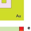
15 Figure legends Figure 1 Design of the tunable C-SRR-GR hybrid metamaterials. a, Schematic of a typical C-SRR. b, Schematic of a GR on a substrate. c, Schematic of a typical unit cell of the proposed C-SRR-GR hybrid metamaterials. d, Simulated x-component of the E-field distribution associated with the LC-resonance of the C- SRR in (a). e, Simulated x-component of the E-field distribution associated with the localized SP resonance of the GR in (b). f, Schematic of a typical unit cell of the proposed C-SRR-GR hybrid metamaterials employing a two-piece C-SRR design. Figure 2 SEM images of a fabricated C-SRR-GR hybrid metamaterial device (HM1). a, SEM image of an array of the C-SRR-GR unit cells. b, Close-up SEM image of a single C-SRR-GR unit cell. Figure 3 Transmission modulation of C-SRR-GR hybrid metamaterials operating at ~10 THz. a, Transmission spectra (normalized to the substrate transmission) of the C-SRR-GR hybrid metamaterial HM1 at different graphene carrier densities in comparison with the transmission spectrum of a reference bare C-SRR array. The transmission spectrum of a GR array exhibiting the localized SP resonances is also shown. b,c, Stacked transmission spectra (5% offset) at varied carrier densities (from the CNP to ~ cm -2 ) of two C- SRR-GR hybrid metamaterial devices, HM1 (b) and HM2 (c), which employ slightly different C-SRR designs. The colored curves in (b) correspond to those in (a) of the same color. d,e, Symbols are the extracted peak frequencies of the two hybridized modes of devices HM1 (d) and HM2 (e) as a function of the carrier density (n 1/4 ) from the corresponding transmission spectra in (b) and (c), respectively. The solid curves are fits of the data points with equation (1) describing the anti-crossing of two strongly coupled resonances, i.e. the localized SP resonances in the GRs (blue dashed line) and the C-SRR LC-resonance (green dashed line). See Supplementary Information for details of the fitting procedure. Figure 4 Simulated spectral response of the tunable C-SRR-GR hybrid metamaterial operating at ~10 THz. a, Simulated transmission spectra of the C-SRR-GR hybrid metamaterial HM1 at various graphene Fermi energies (carrier densities) in comparison with that of a reference bare C-SRR array. The carrier relaxation time of 50 fs is used in this simulation. b,c, Simulated z-component of the E-field distributions associated with the two hybridized modes (transmission peaks), i.e. the bonding mode (b) and the anti-bonding mode (c), at E F =0.4 ev. The upper graphs correspond to the field distributions in the x-y-plane right below the C-SRR-GR unit cell, and the lower graphs correspond to those in the x-z-plane indicated by the dashed line in the upper graphs. d, 15
16 Symbols are the extracted peak frequencies of the two hybridized modes in (a) as a function of the graphene carrier density (n 1/4 ). The solid black curves are fits of the data points using equation (1), with the dashed lines of the same meaning as in Fig. 3d-e. The fits of the corresponding experimental data shown in Fig. 3d are also plotted in solid grey curves for comparison. e, Simulated carrier-density-dependent transmission spectra of a C- SRR-GR hybrid metamaterial in comparison with that of a reference bare C-SRR array, assuming 1 ps for the graphene carrier relaxation time. Figure 5 Transmission modulation of C-SRR-GR hybrid metamaterials operating around 4.5 THz. a,b, Transmission spectra (normalized to the substrate transmission) of the C-SRR-GR hybrid metamaterial devices HM3 (a) and HM4 (b) at different back-gate voltages (graphene carrier densities) in comparison with the transmission spectrum of the corresponding reference bare C-SRR array. The inset in each graph shows a SEM image of a device unit cell. The vertical gray dashed lines indicate the frequency of the THz quantum cascade laser used in the modulation speed measurement. c, Schematic of the parallel electrical contact for all the C- SRR-GR unit cells. d, Symbols are the normalized modulation depth of two hybrid metamaterial devices, HM3 (top) and HM4 (bottom), as a function of modulation frequency. Solid curves are the fits of the measured data based on a standard RC circuit model. 16


17 Figure 1 Figure 2 Figure 3 17

18 Figure 4 Figure 5 18


19 Highly tunable hybrid metamaterials employing split-ring resonators strongly coupled to graphene surface plasmons Peter Q. Liu, 1 * Isaac J. Luxmoore, 2 * Sergey A. Mikhailov, 3 Nadja A. Savostianova, 3 Federico Valmorra, 1 Jerome Faist, 1 Geoffrey R. Nash 2 1 Institute for Quantum Electronics, Department of Physics, ETH Zurich, Zurich CH-8093, Switzerland 2 College of Engineering, Mathematics and Physical Sciences, University of Exeter, Exeter EX4 4QF, United Kingdom 3 Institute of Physics, University of Augsburg, Augsburg 86159, Germany These authors contributed equally to the work. *To whom correspondence should be addressed. qliu@ethz.ch; i.j.luxmoore@exeter.ac.uk S1. Comparison between a conventional C-SRR and a modified two-piece C-SRR designs. By introducing a narrow gap along the horizontal symmetry axis of a conventional C-SRR unit cell, the C-SRR is electrically separated into two parts with minimal influence on the near-field E-field distribution (as indicated by the comparison between Fig. S1a and Fig. S1b) and the transmission spectrum (shown in Fig. S1c). Figure S1 Simulated E-field distributions and transmission spectra of two different C-SRR structures. a, Simulated x-component of the near-field E-field distribution of a conventional (one-piece) C-SRR design. b, Simulated x-component of the near-field E-field distribution of a two-piece C-SRR design. c, Comparison of the transmission spectra of the two C-SRR designs in (a) and (b). S2. Screening of the GR localized plasmons by nearby metallic structures. If the distance between the edges of a GR and the nearby metallic structures (such as the C-SRR in this work) is sufficiently small compared to the thickness of the metallic structures, the localized SP resonance frequency of the GR is reduced as a result of the screening effect from the metal. The collective oscillation of the charge carriers (i.e. the SP resonance) in a GR is a consequence of the restoring force () < 2, (S1)
 metallic structures which may be approximated as infinitely high metallic walls extending in both directions, this restoring")
20 arising due to the charge density fluctuations with the linear charge density, localized near the GR edges and indicated by the positive (+) and negative (-) signs in Fig. S2. In the presence of nearby thick (compared to the distances d 1 and d 2 ) metallic structures which may be approximated as infinitely high metallic walls extending in both directions, this restoring force is modified by the image charges induced in the metal, () , < 2. (S2) As a result, the SP resonance frequency is reduced to = 1 1 2(1 + ) 1 2(1 + ), (S3) where is the unscreened SP resonance frequency of the GR and, =4, /. This calculation provides the theoretical upper limit of the screening effect induced by nearby metallic structures, while the actual reduction of the SP resonance frequency depends on the geometrical details of the structures and can be computed numerically. Figure S2 Schematic of a GR placed between two relatively thick metallic (gold) structures with narrow gaps. Induced image charges are represented by the positive (+) and negative (-) signs in the metallic structures. S3. Fitting procedure of the hybridized modes of the C-SRR-GR hybrid metamaterials. The efficient coupling of the C-SRR LC resonance to the GR localized SP resonance leads to the observed hybridized modes in the transmission spectra of the C-SRR-GR hybrid metamaterials. To quantitatively analyse the carrier density dependent spectral response of these hybrid metamaterials, we have also investigated the tuning of the SP resonances in bare GR arrays (without the C-SRRs). The GR arrays are fabricated on the same SiO 2 /Si substrates used for the hybrid metamaterials, which allow for tuning of the carrier density via the applied back-gate voltage [1]. SiO 2 is a polar dielectric and as such, supports surface optical (SO) phonons, which can couple to SP resonances in the GRs via the long-range Fröhlich interaction [2,3], resulting in multiple surface-plasmon-phonon-polariton (SP3) modes [1,4]. The transmission spectrum of such an array of 400-nm-wide GRs is measured as a function of carrier density and plotted in Fig. S3a. In the measured frequency range, two resonances are observed, labelled P 1 and P 2, which originate from the interaction of the graphene SP and the SO phonon at ~14.5 THz [1]. As the carrier density is increased, there is a monotonic increase in the frequency of both resonances, with the peak positions plotted as a function of carrier density (n 1/4 ) in Fig. S3b.
21 Figure S3 Experimental investigation of a reference array of bare GRs. a, Transmission spectra of an array of GRs (400 nm wide) normalised to the substrate transmission for different values of the carrier density. The labels P 1 and P 2 indicate the two SP3 modes. The curves are offset by 2%. b, Extracted peak frequencies for P 1 and P 2 plotted as a function of n 1/4. The solid grey lines show a fit to the experimental data with Eq. S12. To derive an equation to describe the anti-crossing of the plasmon and SO phonon modes, we consider a 2D layer with the conductivity () lying on the boundary z = 0 of two media with the bulk dielectric functions () and (). The spectrum of electromagnetic waves running along this boundary in the x-direction and localized at this boundary is determined by the dispersion equation (in Gaussian units) () + () + 4 () The conductivity can be described using the Drude Model, which for the case of graphene and neglecting the carrier relaxation is () =, where is the sheet carrier density and is the Fermi velocity. We assume the first medium is vacuum, () =1 and the second has the dielectric function () and consider several special cases. Firstly, the second medium is also vacuum () =1. The dispersion equation then gives =0. (S4) (S5) = 2, where we define as the plasma frequency for graphene in vacuum. In the second case, we assume there is no graphene, i.e. =0, and the second medium is a polar semiconductor with () = ( ), (S6) (S7)
22 where is the frequency of the transverse optical phonons, and and are the dielectric constants at frequencies much lower and much higher than, respectively. The dispersion equation gives and can be rewritten as 1+ () =1+ ( ) =0, = +1 = +1, where is the frequency of the SO phonons. Therefore, the dispersion equation at the interface of a vacuum and a polar semiconductor can be written as 1+ () = (1+ ) =0. Finally, for the case of graphene on the surface of a polar crystal, the dispersion equation is 1+ () 2 = (1+ ) 2 =0, (S8) (S9) (S10) (S11) which leads to the following biquadratic equation, where the two solutions describe the coupled plasmon-phonon modes, + 2,± = +1 ± (S12) To fit the experimental data shown in Fig. S3b, we use Eq. S12 with defined according to Eq. S6 with a slight modification as = 2 / 2 /, (S13) where A is a fitting parameter to take into account the relation between the frequency of the localized SP resonance in a GR and the frequency of a SP wave with the wave vector q in a continuous graphene sheet (Eq. S6); the factor A was numerically found to be ~0.86 in [5], see Figure 1 there (see also [6]). The solid lines in Fig. S3b show a fit to the experimental data using Eq. S12, with = 14.5 THz (ref 1), =3.9 and the fit parameters =2.81 and A=0.77. The lower branch,, is
23 subsequently used to fit the anti-crossing of the C-SRR-GR devices, HM1 and HM2, employing Eq. 1 in the main text with =,, and with = 14.5 THz, =3.9, =2.81 as fixed parameters and A,, as fitting parameters. The same fitting procedure is carried out for the simulated transmission spectra of HM1 in Fig. 4 of the main text. Table S1 lists the fit parameters for the two devices, HM1 and HM2, in comparison with those for the simulated spectra of HM1. Excellent agreement is found between the experimental results and the simulation. Table S1 C-SRR-GR fit parameters. HM1 HM2 Simulation (HM1) A (THz) It is worth pointing out that when evaluating the experimental carrier density of the 400 nm wide GRs at a given back-gate voltage, the parallel-plate capacitor model is not a good approximation in this case, as the GR width is comparable to the thickness d (~300 nm) of the dielectric layer and the edge effect is hence significant. To this end we consider a thin conducting layer of the width W (the GR) lying on a dielectric slab at a distance d from the grounded conducting substrate. The distribution of the electric potential in the free space and in the dielectric is described by the Laplace equation with the boundary conditions =0 at the grounded substrate and = at the GR. Solving this equation with the Green function technique, we reduce the problem to an integral equation for the electron density () inside the GR = / 2 (1 + coth) ()cos ( ) cos( ), / < 2, (S14) where =. Expanding the density () in a series of Chebyshev polynomials (2/) we reduce the problem to an infinite set of algebraic equations for the expansion coefficients. Truncating this set (the convergence is checked and found to be very fast) we get the relation between the average density of electrons in the GR = () and the gate voltage. The resulting ratio of the capacitances / as a function of / at =3.9 (SiO 2 ) is shown in Fig. S4, where is the capacitance predicted by the parallel-plate capacitor model. Figure S4 The calculated ratio / as a function of / at =..
24 S4. Equivalent circuit model of the C-SRR-GR hybrid metamaterials. We introduce an equivalent circuit model as an alternative description of the operating mechanism of the C-SRR-GR hybrid metamaterials, which also provides a more intuitive interpretation of the coupling strength characterized by the parameter in Eq. 1 in the main text. The equivalent circuit diagram for the C-SRR-GR hybrid structure is illustrated in Fig. S5 (enclosed by the dashed square), in which both the C-SRR and the GR are modeled as LC-circuits (losses are neglected for simplicity). The GR is modeled as a parallel LC-circuit because the SP resonance corresponds to enhanced reflection, while the C-SRR is modeled as a series LC-circuit due to enhanced transmission at the resonance. Since the coupling between the C-SRR and the GR is established via the interaction between the near-field electric field of one structure and the charge distribution of the other and vice versa, such a coupling is modeled as a capacitive coupler between the two LC-circuits in the equivalent circuit diagram. Notice that the effective inductor associated with the GR SP resonance is mainly contributed by the kinetic inductance of the charge carriers [7,8]. Figure S5 Equivalent circuit diagram of the C-SRR-GR hybrid metamaterial. Since the C-SRR is excited mainly by the incident electro-magnetic waves whereas the GR is driven mostly by the enhanced electric field in the capacitor gap of the C-SRR, the equivalent circuit for the entire system is constructed as shown in Fig. S5, with and representing the impedance of the free space and the substrate, respectively. Therefore, the transmission peaks correspond to the zeros of the total impedance of the C-SRR-GR equivalent circuit measured between port 2 and port 3, which is straightforwardly derived to be () = ( + + ) ( ) +1. ( + + ) + ( + ) The two zeros of () occur at ± = ( + )+ ( + ) ± ( ( + ) ( + )) Let ( + )=, ( + )=, then Eq. (S16) becomes (S15) (S16)

 and assuming two different carrier relaxation times (50 fs and 100 fs) are")


 in comparison with that of the reference bare C-SRR array, assuming two different carrier relaxation time,")
25 ± = + 2 ± ( ) 2 +, where = ( + )( + ). (S17) The above Eq. S17 reproduces Eq. 1 in the main text describing the anti-crossing behavior of two strongly coupled resonances, and the physical meaning of in this equivalent circuit model is the relative strength of the capacitive coupling. S5. Simulated carrier density dependent spectral response of the C-SRR-GR hybrid metamaterials operating at ~4 THz. The simulated transmission spectra of the hybrid metamaterial device HM3 at various Fermi energies (hence carrier densities) and assuming two different carrier relaxation times (50 fs and 100 fs) are shown in Fig. S6, in comparison with that of the reference bare C-SRR array. The transmission spectra in Fig. S6a exhibit good agreement with the experimental observations in Fig. 5a. On the other hand, the transmission spectra in Fig. S6b clearly reveal the double-peak feature owing to the two hybridized modes in the strong coupling regime, similar to the experimentally observed spectral responses of the 10 THz devices in Fig. 3. From the spectra in Fig. S6b, a coupling strength of ~0.8 THz is extracted for the coupling between the C-SRR LC resonance and the GR localized SP resonance associated with this particular structure. Figure S6 Simulated transmission spectra of tunable C-SRR-GR hybrid metamaterials operating at ~4 THz. a,b, Simulated transmission spectra of device HM3 at various graphene Fermi energies ( E F ) in comparison with that of the reference bare C-SRR array, assuming two different carrier relaxation time, i.e. = 50 fs (a) and = 100 fs (b), respectively. S6. Additional analysis of the modulation speed measurement on the C-SRR-GR hybrid metamaterials. The demonstrated modulation speed of the C-SRR-GR hybrid metamaterials is limited by the effective RC time constant, contributed by both the device itself and the external driving circuit. The total capacitance of the device mainly stems from the capacitor formed between the Si substrate backgate and the C-SRR-GR array, with the ~300 nm SiO 2 layer as the dielectric medium. Since the C- SRR-GR array covers most of the device surface area, the associated capacitance can be estimated using the parallel plate capacitor model, which yields ~115 pf for a 1 mm 1 mm device (HM3) and ~29 pf for a 0.5 mm 0.5 mm device (HM4). The effective total resistance R is further extracted from
26 the modulation speed measurement, and the extracted values are ~80 for HM3 and ~180 for HM4, respectively, excluding the 50 input resistance of the driving voltage source. Thanks to the parallel electrical connection of all the C-SRR-GR unit cells, the resistance associated with the entire C-SRR-GR array is low (Fig. S7) and contributes to only a small fraction of the total resistance. Hence, the major contribution to the device total resistance is from the relatively low-doped Si substrate (resistivity ~10 cm). Since electrical contacts for the current devices are made at the edges of the chip, the current flows in-plane in the Si substrate when charging and discharging the capacitor, resulting in large resistance. Such substrate resistance also depends on the area of the metamaterial field and its location on the chip. Since the measured device HM4 is located closer to the chip center than device HM3 and has smaller area, the substrate resistance seen by HM4 is higher. However, this substrate resistance contribution can be significantly decreased by more than one order of magnitude if electrical contacts are made on the back side of the thin Si substrate, which would facilitate the current to flow perpendicularly instead of in-plane. Such a back contact can be realized with a properly designed wire-grid structure, imposing minimal influence on the transmission of the THz radiation. Alternatively, one can also make use of such hybrid metamaterial structures to modulate the reflection of incident THz radiation, and in this case the Si substrate can be doped much higher. Figure S7 Measured source-drain resistance (R SD ) of the entire C-SRR-GR array (HM3) as a function of the back-gate voltage (V G ). References [1] Luxmoore, I. J. et al. Strong coupling in the far-infrared between graphene plasmons and the surface optical phonons of silicon dioxide. ACS Photon. 1, (2014). [2] Wang, S. Q., Mahan, G. D. Electron scattering from surface excitations. Phys. Rev. B 6, (1972). [3] Fratini, S., Guinea, F. Substrate-limited electron dynamics in graphene. Phys. Rev. B 77, (2008). [4] Yan, H. et al. Damping pathways of mid-infrared plasmons in graphene nanostructures. Nature Photon. 7, (2013). [5] Mikhailov, S. A., Savostianova, N. A. Microwave response of a two-dimensional electron stripe. Phys. Rev. B 71, (2005). [6] Nikitin, A. Y., Low, T., Martin-Moreno, L. Anomalous reflection phase of graphene plasmons and its influence on resonators. Phys. Rev. B 90, (2014). [7] Burke, P. J., Spielman, I. B., Eisenstein, J. P., Pfeiffer, L. N., West, K. W. High frequency conductivity of the high-mobility two-dimensional electron gas. Appl. Phys. Lett. 76, (2000). [8] Dyer, G. C. et al. Induced transparency by coupling of Tamm and defect states in tuable terahertz plasmonic crystals. Nature Photon. 7, (2013).
Highly Confined Tunable Mid-Infrared Plasmonics in Graphene Nanoresonators
 Supplementary Information for Highly Confined Tunable Mid-Infrared Plasmonics in Graphene Nanoresonators by Victor W. Brar, Min Seok Jang, Michelle Sherrott, Josue J. Lopez and Harry Atwater 1 Approximating
An efficient way to reduce losses of left-handed metamaterials
 An efficient way to reduce losses of left-handed metamaterials Jiangfeng Zhou 1,2,, Thomas Koschny 1,3 and Costas M. Soukoulis 1,3 1 Ames Laboratory and Department of Physics and Astronomy,Iowa State University,
Hybrid Surface-Phonon-Plasmon Polariton Modes in Graphene /
 Supplementary Information: Hybrid Surface-Phonon-Plasmon Polariton Modes in Graphene / Monolayer h-bn stacks Victor W. Brar 1,2, Min Seok Jang 3,, Michelle Sherrott 1, Seyoon Kim 1, Josue J. Lopez 1, Laura
A Broadband Flexible Metamaterial Absorber Based on Double Resonance
 Progress In Electromagnetics Research Letters, Vol. 46, 73 78, 2014 A Broadband Flexible Metamaterial Absorber Based on Double Resonance ong-min Lee* Abstract We present a broadband microwave metamaterial
Flute-Model Acoustic Metamaterials with Simultaneously. Negative Bulk Modulus and Mass Density
 Flute-Model Acoustic Metamaterials with Simultaneously Negative Bulk Modulus and Mass Density H. C. Zeng, C. R. Luo, H. J. Chen, S. L. Zhai and X. P. Zhao * Smart Materials Laboratory, Department of Applied
Demonstration of Near-Infrared Negative-Index Materials
 Demonstration of Near-Infrared Negative-Index Materials Shuang Zhang 1, Wenjun Fan 1, N. C. Panoiu 2, K. J. Malloy 1, R. M. Osgood 2 and S. R. J. Brueck 2 1. Center for High Technology Materials and Department
Workshop on New Materials for Renewable Energy
 2286-6 Workshop on New Materials for Renewable Energy 31 October - 11 November 201 Metamaterials: Past, Present, and Future Nonlinear Physics Centre Research School of Physics and Engineering The Australian
Graphene photodetectors with ultra-broadband and high responsivity at room temperature
 SUPPLEMENTARY INFORMATION DOI: 10.1038/NNANO.2014.31 Graphene photodetectors with ultra-broadband and high responsivity at room temperature Chang-Hua Liu 1, You-Chia Chang 2, Ted Norris 1.2* and Zhaohui
Strong coupling in the far-infrared between graphene plasmons and the
 Strong coupling in the far-infrared between graphene plasmons and the surface optical phonons of silicon dioxide I. J. Luxmoore 1,a), C. H. Gan 1, P. Q. Liu 2, F. Valmorra 2, P. Li 1, J. Faist 2, and G.
Supplementary material for High responsivity mid-infrared graphene detectors with antenna-enhanced photo-carrier generation and collection
 Supplementary material for High responsivity mid-infrared graphene detectors with antenna-enhanced photo-carrier generation and collection Yu Yao 1, Raji Shankar 1, Patrick Rauter 1, Yi Song 2, Jing Kong
Nonlinear Electrodynamics and Optics of Graphene
 Nonlinear Electrodynamics and Optics of Graphene S. A. Mikhailov and N. A. Savostianova University of Augsburg, Institute of Physics, Universitätsstr. 1, 86159 Augsburg, Germany E-mail: sergey.mikhailov@physik.uni-augsburg.de
Wednesday 3 September Session 3: Metamaterials Theory (16:15 16:45, Huxley LT308)
") Session 3: Metamaterials Theory (16:15 16:45, Huxley LT308) (invited) TBC Session 3: Metamaterials Theory (16:45 17:00, Huxley LT308) Light trapping states in media with longitudinal electric waves D McArthur,
Session 3: Metamaterials Theory (16:15 16:45, Huxley LT308) (invited) TBC Session 3: Metamaterials Theory (16:45 17:00, Huxley LT308) Light trapping states in media with longitudinal electric waves D McArthur,
Supplementary Information for. Vibrational Spectroscopy at Electrolyte Electrode Interfaces with Graphene Gratings
 Supplementary Information for Vibrational Spectroscopy at Electrolyte Electrode Interfaces with Graphene Gratings Supplementary Figure 1. Simulated from pristine graphene gratings at different Fermi energy
Electronically Tunable Perfect Absorption in Graphene
 Electronically Tunable Perfect Absorption in Graphene Seyoon Kim 1,, Min Seok Jang 1,2,, Victor W. Brar 1,3,4,, Kelly W. Mauser 1, and Harry A. Atwater 1,3,* * haa@caltech.edu Equally contributed authors
Supplementary Methods A. Sample fabrication
 Supplementary Methods A. Sample fabrication Supplementary Figure 1(a) shows the SEM photograph of a typical sample, with three suspended graphene resonators in an array. The cross-section schematic is
Enhancing and suppressing radiation with some permeability-near-zero structures
 Enhancing and suppressing radiation with some permeability-near-zero structures Yi Jin 1,2 and Sailing He 1,2,3,* 1 Centre for Optical and Electromagnetic Research, State Key Laboratory of Modern Optical
arxiv: v1 [physics.optics] 17 Jan 2013
![arxiv: v1 [physics.optics] 17 Jan 2013](/thumbs/95/122987545.jpg "arxiv: v1 [physics.optics] 17 Jan 2013") Three Dimensional Broadband Tunable Terahertz Metamaterials Kebin Fan,1 Andrew C. Strikwerda,2 Xin Zhang,1, and Richard D. Averitt2, arxiv:1301.3977v1 [physics.optics] 17 Jan 2013 1 Department of Mechanical
Three Dimensional Broadband Tunable Terahertz Metamaterials Kebin Fan,1 Andrew C. Strikwerda,2 Xin Zhang,1, and Richard D. Averitt2, arxiv:1301.3977v1 [physics.optics] 17 Jan 2013 1 Department of Mechanical
Supplementary Figure S1 SEM and optical images of Si 0.6 H 0.4 colloids. a, SEM image of Si 0.6 H 0.4 colloids. b, The size distribution of Si 0.
 Supplementary Figure S1 SEM and optical images of Si 0.6 H 0.4 colloids. a, SEM image of Si 0.6 H 0.4 colloids. b, The size distribution of Si 0.6 H 0.4 colloids. The standard derivation is 4.4 %. Supplementary
Controlling Graphene Ultrafast Hot Carrier Response from Metal-like. to Semiconductor-like by Electrostatic Gating
 Controlling Graphene Ultrafast Hot Carrier Response from Metal-like to Semiconductor-like by Electrostatic Gating S.-F. Shi, 1,2* T.-T. Tang, 1 B. Zeng, 1 L. Ju, 1 Q. Zhou, 1 A. Zettl, 1,2,3 F. Wang 1,2,3
Supplementary Figure 1 Schematics of an optical pulse in a nonlinear medium. A Gaussian optical pulse propagates along z-axis in a nonlinear medium
 Supplementary Figure 1 Schematics of an optical pulse in a nonlinear medium. A Gaussian optical pulse propagates along z-axis in a nonlinear medium with thickness L. Supplementary Figure Measurement of
Nanophysics: Main trends
 Nano-opto-electronics Nanophysics: Main trends Nanomechanics Main issues Light interaction with small structures Molecules Nanoparticles (semiconductor and metallic) Microparticles Photonic crystals Nanoplasmonics
Nanoscale optical circuits: controlling light using localized surface plasmon resonances
 Nanoscale optical circuits: controlling light using localized surface plasmon resonances T. J. Davis, D. E. Gómez and K. C. Vernon CSIRO Materials Science and Engineering Localized surface plasmon (LSP)
Extinction properties of a sphere with negative permittivity and permeability
 PERGAMON Solid State Communications 116 (2000) 411 415 www.elsevier.com/locate/ssc Extinction properties of a sphere with negative permittivity and permeability R. Ruppin* Department of Physics and Applied
Doctor of Philosophy
 FEMTOSECOND TIME-DOMAIN SPECTROSCOPY AND NONLINEAR OPTICAL PROPERTIES OF IRON-PNICTIDE SUPERCONDUCTORS AND NANOSYSTEMS A Thesis Submitted for the degree of Doctor of Philosophy IN THE FACULTY OF SCIENCE
Black phosphorus: A new bandgap tuning knob
 Black phosphorus: A new bandgap tuning knob Rafael Roldán and Andres Castellanos-Gomez Modern electronics rely on devices whose functionality can be adjusted by the end-user with an external knob. A new
Superconductivity Induced Transparency
 Superconductivity Induced Transparency Coskun Kocabas In this paper I will discuss the effect of the superconducting phase transition on the optical properties of the superconductors. Firstly I will give
Tuning of superconducting niobium nitride terahertz metamaterials
 Tuning of superconducting niobium nitride terahertz metamaterials Jingbo Wu, Biaobing Jin,* Yuhua Xue, Caihong Zhang, Hao Dai, Labao Zhang, Chunhai Cao, Lin Kang, Weiwei Xu, Jian Chen and Peiheng Wu Research
Coherent thermal emission by excitation of magnetic polaritons between periodic strips and a metallic film
 Coherent thermal emission by excitation of magnetic polaritons between periodic strips and a metallic film B. J. Lee, L. P. Wang, and Z. M. Zhang George W. Woodruff School of Mechanical Engineering Georgia
Raman Imaging and Electronic Properties of Graphene
 Raman Imaging and Electronic Properties of Graphene F. Molitor, D. Graf, C. Stampfer, T. Ihn, and K. Ensslin Laboratory for Solid State Physics, ETH Zurich, 8093 Zurich, Switzerland ensslin@phys.ethz.ch
Author(s) Tamayama, Y; Nakanishi, T; Sugiyama. Citation PHYSICAL REVIEW B (2006), 73(19)
 Tamayama, Y; Nakanishi, T; Sugiyama. Citation PHYSICAL REVIEW B (2006), 73(19)") Observation of Brewster's effect fo Titleelectromagnetic waves in metamateri theory Author(s) Tamayama, Y; Nakanishi, T; Sugiyama Citation PHYSICAL REVIEW B (2006), 73(19) Issue Date 2006-05 URL http://hdl.handle.net/2433/39884
Observation of Brewster's effect fo Titleelectromagnetic waves in metamateri theory Author(s) Tamayama, Y; Nakanishi, T; Sugiyama Citation PHYSICAL REVIEW B (2006), 73(19) Issue Date 2006-05 URL http://hdl.handle.net/2433/39884
Super-reflection and Cloaking Based on Zero Index Metamaterial
 Super-reflection and Cloaking Based on Zero Index Metamaterial Jiaming Hao, Wei Yan, and Min Qiu Photonics and Microwave ngineering, Royal Institute of Technology (KTH), lectrum 9, 164 4, Kista, Sweden
Strong light matter coupling in two-dimensional atomic crystals
 SUPPLEMENTARY INFORMATION DOI: 10.1038/NPHOTON.2014.304 Strong light matter coupling in two-dimensional atomic crystals Xiaoze Liu 1, 2, Tal Galfsky 1, 2, Zheng Sun 1, 2, Fengnian Xia 3, Erh-chen Lin 4,
Magnetic response of split-ring resonator metamaterials: From effective medium dispersion to photonic band gaps
 PRAMANA c Indian Academy of Sciences Vol. 78, No. 3 journal of March 2012 physics pp. 483 492 Magnetic response of split-ring resonator metamaterials: From effective medium dispersion to photonic band
Nonlinear Metamaterial Composite Structure with Tunable Tunneling Frequency
 Progress In Electromagnetics Research Letters, Vol. 71, 91 96, 2017 Nonlinear Metamaterial Composite Structure with Tunable Tunneling Frequency Tuanhui Feng *,HongpeiHan,LiminWang,andFeiYang Abstract A
90 degree polarization rotator using a bilayered chiral metamaterial with giant optical activity
 90 degree polarization rotator using a bilayered chiral metamaterial with giant optical activity Yuqian Ye 1 and Sailing He 1,2,* 1 Centre for Optical and Electromagnetic Research, State Key Laboratory
PHYSICAL REVIEW B 71,
 Coupling of electromagnetic waves and superlattice vibrations in a piezomagnetic superlattice: Creation of a polariton through the piezomagnetic effect H. Liu, S. N. Zhu, Z. G. Dong, Y. Y. Zhu, Y. F. Chen,
(a) (b) Supplementary Figure 1. (a) (b) (a) Supplementary Figure 2. (a) (b) (c) (d) (e)
 (b) Supplementary Figure 1. (a) (b) (a) Supplementary Figure 2. (a) (b) (c) (d) (e)") (a) (b) Supplementary Figure 1. (a) An AFM image of the device after the formation of the contact electrodes and the top gate dielectric Al 2 O 3. (b) A line scan performed along the white dashed line
(a) (b) Supplementary Figure 1. (a) An AFM image of the device after the formation of the contact electrodes and the top gate dielectric Al 2 O 3. (b) A line scan performed along the white dashed line
SUPPLEMENTARY INFORMATION
 Supplementary Information: Photocurrent generation in semiconducting and metallic carbon nanotubes Maria Barkelid 1*, Val Zwiller 1 1 Kavli Institute of Nanoscience, Delft University of Technology, Delft,
Highly Sensitive and Wide-Band Tunable Terahertz Response of Plasma Wave based on Graphene Field Effect Transistors
 Supplementary Information Highly Sensitive and Wide-Band Tunable Terahertz Response of Plasma Wave based on Graphene Field Effect Transistors Lin Wang, Xiaoshuang Chen *, Anqi Yu, Yang Zhang, Jiayi Ding
Supplementary Information. Boron nitride nanoresonators for phonon-enhanced molecular vibrational spectroscopy at the strong coupling limit
 Supplementary Information Boron nitride nanoresonators for phonon-enhanced molecular vibrational spectroscopy at the strong coupling limit Marta Autore 1, Peining Li 1, Irene Dolado 1, Francisco J. Alfaro-Mozaz
Observation of topological surface state quantum Hall effect in an intrinsic three-dimensional topological insulator
 Observation of topological surface state quantum Hall effect in an intrinsic three-dimensional topological insulator Authors: Yang Xu 1,2, Ireneusz Miotkowski 1, Chang Liu 3,4, Jifa Tian 1,2, Hyoungdo
EPSILON-NEAR-ZERO (ENZ) AND MU-NEAR-ZERO (MNZ) MATERIALS
 AND MU-NEAR-ZERO (MNZ) MATERIALS") EPSILON-NEAR-ZERO (ENZ) AND MU-NEAR-ZERO (MNZ) MATERIALS SARAH NAHAR CHOWDHURY PURDUE UNIVERSITY 1 Basics Design ENZ Materials Lumped circuit elements Basics Decoupling Direction emission Tunneling Basics
EPSILON-NEAR-ZERO (ENZ) AND MU-NEAR-ZERO (MNZ) MATERIALS SARAH NAHAR CHOWDHURY PURDUE UNIVERSITY 1 Basics Design ENZ Materials Lumped circuit elements Basics Decoupling Direction emission Tunneling Basics
Near-field interactions in electric inductive capacitive resonators for metamaterials
 IOP PUBLISHING JOURNAL OF PHYSICS D: APPLIED PHYSICS J. Phys. D: Appl. Phys. 45 (2012) 485101 (7pp) doi:10.1088/0022-3727/45/48/485101 Near-field interactions in electric inductive capacitive resonators
PLASMONICS/METAMATERIALS
 PLASMONICS/METAMATERIALS Interconnects Optical processing of data Subwavelength confinement Electrodes are in place Coupling to other on-chip devices Combination of guiding, detection, modulation, sensing
Left-handed and right-handed metamaterials composed of split ring resonators and strip wires
 Left-handed and right-handed metamaterials composed of split ring resonators and strip wires J. F. Woodley, M. S. Wheeler, and M. Mojahedi Electromagnetics Group, Edward S. Rogers Sr. Department of Electrical
 Johnson, N.P. and Khokhar, A.Z. and Chong, H.M.H. and De La Rue, R.M. and McMeekin, S. (2006) Characterisation at infrared wavelengths of metamaterials formed by thin-film metallic split-ring resonator
Dielectric Meta-Reflectarray for Broadband Linear Polarization Conversion and Optical Vortex Generation
 Supporting Information Dielectric Meta-Reflectarray for Broadband Linear Polarization Conversion and Optical Vortex Generation Yuanmu Yang, Wenyi Wang, Parikshit Moitra, Ivan I. Kravchenko, Dayrl P. Briggs,
A SYMMETRICAL DUAL-BAND TERAHERTZ META- MATERIAL WITH CRUCIFORM AND SQUARE LOOPS. Microsystem and Information Technology, Shanghai , China
 Progress In Electromagnetics Research C, Vol. 33, 259 267, 2012 A SYMMETRICAL DUAL-BAND TERAHERTZ META- MATERIAL WITH CRUCIFORM AND SQUARE LOOPS B. Li 1, *, L. X. He 2, Y. Z. Yin 1, W. Y. Guo 2, 3, and
On the signs of the imaginary parts of the effective permittivity and permeability in metamaterials
 1016 J. Opt. Soc. Am. B/ Vol. 27, No. 5/ May 2010 J. Woodley and M. Mojahedi On the signs of the imaginary parts of the effective permittivity and permeability in metamaterials J. Woodley 1, * and M. Mojahedi
SUPPLEMENTARY INFORMATION
 In the format provided by the authors and unedited. SUPPLEMENTARY INFORMATION DOI: 10.1038/NPHOTON.017.65 Imaging exciton-polariton transport in MoSe waveguides F. Hu 1,, Y. Luan 1,, M. E. Scott 3, J.
Design and Characterization of a Dual-Band Metamaterial Absorber Based on Destructive Interferences
 Progress In Electromagnetics Research C, Vol. 47, 95, 24 Design and Characterization of a Dual-Band Metamaterial Absorber Based on Destructive Interferences Saeid Jamilan, *, Mohammad N. Azarmanesh, and
Impact of disorder and topology in two dimensional systems at low carrier densities
 Impact of disorder and topology in two dimensional systems at low carrier densities A Thesis Submitted For the Degree of Doctor of Philosophy in the Faculty of Science by Mohammed Ali Aamir Department
Supplementary Figure 2 Photoluminescence in 1L- (black line) and 7L-MoS 2 (red line) of the Figure 1B with illuminated wavelength of 543 nm.
 and 7L-MoS 2 (red line) of the Figure 1B with illuminated wavelength of 543 nm.") PL (normalized) Intensity (arb. u.) 1 1 8 7L-MoS 1L-MoS 6 4 37 38 39 4 41 4 Raman shift (cm -1 ) Supplementary Figure 1 Raman spectra of the Figure 1B at the 1L-MoS area (black line) and 7L-MoS area (red
PL (normalized) Intensity (arb. u.) 1 1 8 7L-MoS 1L-MoS 6 4 37 38 39 4 41 4 Raman shift (cm -1 ) Supplementary Figure 1 Raman spectra of the Figure 1B at the 1L-MoS area (black line) and 7L-MoS area (red
arxiv: v1 [cond-mat.supr-con] 8 Sep 2010
![arxiv: v1 [cond-mat.supr-con] 8 Sep 2010](/thumbs/91/106922039.jpg "arxiv: v1 [cond-mat.supr-con] 8 Sep 2010") Tuning the Resonance in High Temperature Superconducting Terahertz Metamaterials Hou-Tong Chen, Hao Yang, Ranjan Singh, John F. O Hara, Abul K. Azad, Stuart A. Trugman, Q. X. Jia, and Antoinette J. Taylor
Tuning the Resonance in High Temperature Superconducting Terahertz Metamaterials Hou-Tong Chen, Hao Yang, Ranjan Singh, John F. O Hara, Abul K. Azad, Stuart A. Trugman, Q. X. Jia, and Antoinette J. Taylor
Chapter 5. Photonic Crystals, Plasmonics, and Metamaterials
 Chapter 5. Photonic Crystals, Plasmonics, and Metamaterials Reading: Saleh and Teich Chapter 7 Novotny and Hecht Chapter 11 and 12 1. Photonic Crystals Periodic photonic structures 1D 2D 3D Period a ~
Supplementary Information
 S1 Supplementary Information S2 Forward Backward Forward Backward Normalized to Normalized to Supplementary Figure 1 Maximum local field ratio and transmission coefficient. Maximum local field ratio (green
High transmittance left-handed materials involving symmetric split-ring resonators
 Photonics and Nanostructures Fundamentals and Applications 5 (2007) 149 155 www.elsevier.com/locate/photonics High transmittance left-handed materials involving symmetric split-ring resonators N. Katsarakis
Monolayer Black Phosphorus
 Supporting Information: Localized Surface Plasmons in Nanostructured Monolayer Black Phosphorus Zizhuo Liu and Koray Aydin* Department of Electrical Engineering and Computer Science, Northwestern University,
Multiple Fano Resonances Structure for Terahertz Applications
 Progress In Electromagnetics Research Letters, Vol. 50, 1 6, 2014 Multiple Fano Resonances Structure for Terahertz Applications Hadi Amarloo *, Daniel M. Hailu, and Safieddin Safavi-Naeini Abstract A new
A Novel Design of Photonic Crystal Lens Based on Negative Refractive Index
 PIERS ONLINE, VOL. 4, NO. 2, 2008 296 A Novel Design of Photonic Crystal Lens Based on Negative Refractive Index S. Haxha 1 and F. AbdelMalek 2 1 Photonics Group, Department of Electronics, University
Negative Index of Refraction in Optical Metamaterials
 1 Negative Index of Refraction in Optical Metamaterials V. M. Shalaev, W. Cai, U. Chettiar, H.-K. Yuan, A. K. Sarychev, V. P. Drachev, and A. V. Kildishev School of Electrical and Computer Engineering,
Left-handed materials: Transfer matrix method studies
 Left-handed materials: Transfer matrix method studies Peter Markos and C. M. Soukoulis Outline of Talk What are Metamaterials? An Example: Left-handed Materials Results of the transfer matrix method Negative
transmission reflection absorption
 Optical Cages V. Kumar*, J. P. Walker* and H. Grebel The Electronic Imaging Center and the ECE department at NJIT, Newark, NJ 0702. grebel@njit.edu * Contributed equally Faraday Cage [], a hollow structure
Optimizing the performance of metal-semiconductor-metal photodetectors by embedding nanoparticles in the absorption layer
 Journal of Electrical and Electronic Engineering 2015; 3(2-1): 78-82 Published online February 10, 2015 (http://www.sciencepublishinggroup.com/j/jeee) doi: 10.11648/j.jeee.s.2015030201.27 ISSN: 2329-1613
Towards the Lasing Spaser: Controlling. Metamaterial Optical Response with Semiconductor. Quantum Dots
 Towards the Lasing Spaser: Controlling Metamaterial Optical Response with Semiconductor Quantum Dots E. Plum, V. A. Fedotov, P. Kuo, D. P. Tsai, and N. I. Zheludev,, Optoelectronics Research Centre, University
SCATTERING CROSS SECTION OF A META-SPHERE
 Progress In Electromagnetics Research Letters, Vol. 9, 85 91, 009 SCATTERING CROSS SECTION OF A META-SPHERE A. Alexopoulos Electronic Warfare and Radar Division Defence Science and Technology Organisation
Negative refractive index response of weakly and strongly coupled optical metamaterials.
 Negative refractive index response of weakly and strongly coupled optical metamaterials. Jiangfeng Zhou, 1 Thomas Koschny, 1, Maria Kafesaki, and Costas M. Soukoulis 1, 1 Ames Laboratory and Department
SUPPLEMENTARY INFORMATION
 doi:10.1038/nature12036 We provide in the following additional experimental data and details on our demonstration of an electrically pumped exciton-polariton laser by supplementing optical and electrical
arrays for mid-infrared plasmonics
 Scalable and tunable periodic graphene nano-hole arrays for mid-infrared plasmonics Kavitha K. Gopalan*, Bruno Paulillo*, David M.A. Mackenzie +, Daniel Rodrigo*, Nestor Bareza*, Patrick R. Whelan +, Abhay
GHz magnetic response of split ring resonators
 Photonics and Nanostructures Fundamentals and Applications 2 (2004) 155 159 www.elsevier.com/locate/photonics GHz magnetic response of split ring resonators Lei Zhang a, G. Tuttle a, C.M. Soukoulis b,
New Concept Conformal Antennas Utilizing Metamaterial and Transformation Optics
 New Concept Conformal Antennas Utilizing Metamaterial and Transformation Optics The MIT Faculty has made this article openly available. Please share how this access benefits you. Your story matters. Citation
Configurable metamaterial absorber with pseudo wideband spectrum
 Configurable metamaterial absorber with pseudo wideband spectrum Weiren Zhu, 1, Yongjun Huang, 2 Ivan D. Rukhlenko, 1 Guangjun Wen, 2 and Malin Premaratne 1 1 Advanced Computing and Simulation Laboratory
Supporting Information. by Hexagonal Boron Nitride
 Supporting Information High Velocity Saturation in Graphene Encapsulated by Hexagonal Boron Nitride Megan A. Yamoah 1,2,, Wenmin Yang 1,3, Eric Pop 4,5,6, David Goldhaber-Gordon 1 * 1 Department of Physics,
Broadband Subwavelength Imaging with a Wire Medium Slab Loaded with Graphene Sheets
 Broadband Subwavelength Imaging with a Wire Medium Slab Loaded with Graphene Sheets Ali Forouzmand and Alexander B. Yakovlev Center for Applied Electromagnetic Systems Research (CAESR) Department of Electrical
History of photonic crystals and metamaterials. However, many serious obstacles must be overcome before the impressive possibilities
 TECHNICAL NOTEBOOK I back to basics BACK TO BASICS: History of photonic crystals and metamaterials Costas M. SOUKOULIS 1,2 1 Ames Laboratory and Department of Physics, Iowa State University, Ames, Iowa,
Terahertz antireflection coating enabled by a subwavelength metallic mesh capped with a thin dielectric film
 Invited Paper Terahertz antireflection coating enabled by a subwavelength metallic mesh capped with a thin dielectric film Li Huang 1*, Beibei Zeng 2, Chun-Chieh Chang 2 and Hou-Tong Chen 2* 1 Physics
Introduction to Metamaterials. Richard D. Averitt
 Introduction to Metamaterials Richard D. Averitt Research Themes Equilibrium is when all of the fast stuff has happened, and all of the slow stuff hasn t. - Feynman Metamaterials: a new field D. R. Smith,
Analysis of Metamaterial Cloaks Using Circular Split Ring Resonator Structures
 Copyright 216 Tech Science Press CMC, Vol.53, No.3, pp.132-14, 216 Analysis of Metamaterial Cloaks Using Circular Split Ring Resonator Structures Susan Thomas 1 and Dr. Balamati Choudhury 2 Abstract A
Supplemental Materials
 Supplemental Materials On the modeling of graphene layer by a thin dielectric Modeling graphene as a D surface having an appropriate value of surface conductivity σ is an accurate approach for a semiclassical
B. Zhu, Z. Wang, C. Huang, Y. Feng, J. Zhao, and T. Jiang Department of Electronic Science and Engineering Nanjing University Nanjing , China
 Progress In Electromagnetics Research, PIER 101, 231 239, 2010 POLARIZATION INSENSITIVE METAMATERIAL ABSORBER WITH WIDE INCIDENT ANGLE B. Zhu, Z. Wang, C. Huang, Y. Feng, J. Zhao, and T. Jiang Department
vapour deposition. Raman peaks of the monolayer sample grown by chemical vapour
 Supplementary Figure 1 Raman spectrum of monolayer MoS 2 grown by chemical vapour deposition. Raman peaks of the monolayer sample grown by chemical vapour deposition (S-CVD) are peak which is at 385 cm
Optical Properties of Left-Handed Materials by Nathaniel Ferraro 01
 Optical Properties of Left-Handed Materials by Nathaniel Ferraro 1 Abstract Recently materials with the unusual property of having a simultaneously negative permeability and permittivity have been tested
Progress In Electromagnetics Research, PIER 35, , 2002
 Progress In Electromagnetics Research, PIER 35, 315 334, 2002 NUMERICAL STUDIES OF LEFT HANDED METAMATERIALS C. D. Moss, T. M. Grzegorczyk, Y. Zhang, and J. A. Kong Research Laboratory of Electronics Massachusetts
GHZ ELECTRICAL PROPERTIES OF CARBON NANOTUBES ON SILICON DIOXIDE MICRO BRIDGES
 GHZ ELECTRICAL PROPERTIES OF CARBON NANOTUBES ON SILICON DIOXIDE MICRO BRIDGES SHENG F. YEN 1, HAROON LAIS 1, ZHEN YU 1, SHENGDONG LI 1, WILLIAM C. TANG 1,2, AND PETER J. BURKE 1,2 1 Electrical Engineering
SUPPLEMENTARY INFORMATION
 Ultra-sparse metasurface for high reflection of low-frequency sound based on artificial Mie resonances Y. Cheng, 1,2 C. Zhou, 1 B.G. Yuan, 1 D.J. Wu, 3 Q. Wei, 1 X.J. Liu 1,2* 1 Key Laboratory of Modern
SUPPLEMENTARY INFORMATION
 doi:10.1038/nature11231 Materials and Methods: Sample fabrication: Highly oriented VO 2 thin films on Al 2 O 3 (0001) substrates were deposited by reactive sputtering from a vanadium target through reactive
TUNABLE METAMATERIAL DESIGN COMPOSED OF TRIANGULAR SPLIT RING RESONATOR AND WIRE STRIP FOR S- AND C- MICROWAVE BANDS
 Progress In Electromagnetics Research B, Vol. 22, 341 357, 2010 TUNABLE METAMATERIAL DESIGN COMPOSED OF TRIANGULAR SPLIT RING RESONATOR AND WIRE STRIP FOR S- AND C- MICROWAVE BANDS C. Sabah Johann Wolfgang
Terahertz sensing and imaging based on carbon nanotubes:
 Terahertz sensing and imaging based on carbon nanotubes: Frequency-selective detection and near-field imaging Yukio Kawano RIKEN, JST PRESTO ykawano@riken.jp http://www.riken.jp/lab-www/adv_device/kawano/index.html
Supplementary Figure 1. Selected area electron diffraction (SAED) of bilayer graphene and tblg. (a) AB
 of bilayer graphene and tblg. (a) AB") Supplementary Figure 1. Selected area electron diffraction (SAED) of bilayer graphene and tblg. (a) AB stacked bilayer graphene (b), (c), (d), (e), and (f) are twisted bilayer graphene with twist angle
Supplementary Figure 1. Selected area electron diffraction (SAED) of bilayer graphene and tblg. (a) AB stacked bilayer graphene (b), (c), (d), (e), and (f) are twisted bilayer graphene with twist angle
A Study on the Suitability of Indium Nitride for Terahertz Plasmonics
 A Study on the Suitability of Indium Nitride for Terahertz Plasmonics Arjun Shetty 1*, K. J. Vinoy 1, S. B. Krupanidhi 2 1 Electrical Communication Engineering, Indian Institute of Science, Bangalore,
sgsp agsp W=20nm W=50nm Re(n eff (e) } Re{E z Im{E x Supplementary Figure 1: Gap surface plasmon modes in MIM waveguides.
 } Re{E z Im{E x Supplementary Figure 1: Gap surface plasmon modes in MIM waveguides.") (a) 2.4 (b) (c) W Au y Electric field (a.u) x SiO 2 (d) y Au sgsp x Energy (ev) 2. 1.6 agsp W=5nm W=5nm 1.2 1 2 3 4.1.1 1 1 Re(n eff ) -1-5 5 1 x (nm) W = 2nm E = 2eV Im{E x } Re{E z } sgsp Electric field
(a) 2.4 (b) (c) W Au y Electric field (a.u) x SiO 2 (d) y Au sgsp x Energy (ev) 2. 1.6 agsp W=5nm W=5nm 1.2 1 2 3 4.1.1 1 1 Re(n eff ) -1-5 5 1 x (nm) W = 2nm E = 2eV Im{E x } Re{E z } sgsp Electric field
Monolayer Semiconductors
 Monolayer Semiconductors Gilbert Arias California State University San Bernardino University of Washington INT REU, 2013 Advisor: Xiaodong Xu (Dated: August 24, 2013) Abstract Silicon may be unable to
SUPPLEMENTARY INFORMATION
 DOI: 1.138/NNANO.215.33 Epitaxial graphene quantum dots for high-performance terahertz bolometers Abdel El Fatimy *, Rachael L. Myers-Ward, Anthony K. Boyd, Kevin M. Daniels, D. Kurt Gaskill, and Paola
Supplementary Figure S1. AFM images of GraNRs grown with standard growth process. Each of these pictures show GraNRs prepared independently,
 Supplementary Figure S1. AFM images of GraNRs grown with standard growth process. Each of these pictures show GraNRs prepared independently, suggesting that the results is reproducible. Supplementary Figure
Quantum Phenomena & Nanotechnology (4B5)
") Quantum Phenomena & Nanotechnology (4B5) The 2-dimensional electron gas (2DEG), Resonant Tunneling diodes, Hot electron transistors Lecture 11 In this lecture, we are going to look at 2-dimensional electron
Quantum Phenomena & Nanotechnology (4B5) The 2-dimensional electron gas (2DEG), Resonant Tunneling diodes, Hot electron transistors Lecture 11 In this lecture, we are going to look at 2-dimensional electron
U-Shaped Nano-Apertures for Enhanced Optical Transmission and Resolution
 U-Shaped Nano-Apertures for Enhanced Optical Transmission and Resolution Mustafa Turkmen 1,2,3, Serap Aksu 3,4, A. Engin Çetin 2,3, Ahmet A. Yanik 2,3, Alp Artar 2,3, Hatice Altug 2,3,4, * 1 Electrical
Angular-Stability Low-Profile Miniaturized Frequency Selective Surface Based on Complementary Structure
 Progress In Electromagnetics Research M, Vol. 57, 119 128, 2017 Angular-Stability Low-Profile Miniaturized Frequency Selective Surface Based on Complementary Structure Wenxing Li and Yuanyuan Li * Abstract
Canalization of Sub-wavelength Images by Electromagnetic Crystals
 Progress In Electromagnetics Research Symposium 2005, Hangzhou, China, August 22-26 37 Canalization of Sub-wavelength Images by Electromagnetic Crystals P. A. Belov 1 and C. R. Simovski 2 1 Queen Mary
07/7001 METAMATERIALS FOR SPACE APPLICATIONS
 07/7001 METAMATERIALS FOR SPACE APPLICATIONS Type of activity: Medium Study (4 months, 25 KEUR) Background and Motivation Brief description of the Metamaterial concept Metamaterials could be considered
Electromagnetic Metamaterials
 Electromagnetic Metamaterials Dr. Alkim Akyurtlu Center for Electromagnetic Materials and Optical Systems University of Massachusetts Lowell September 19, 2006 Objective Outline Background on Metamaterials