High-speed waveguide-coupled graphene-on-graphene optical modulators. Steven J. Koester 1 and Mo Li 2
|
|
|
- Allan Burke
- 5 years ago
- Views:
Transcription
1 High-speed waveguide-coupled graphene-on-graphene optical modulators Steven J. Koester 1 and Mo Li 2 Department of Electrical and Computer Engineering, University of Minnesota-Twin Cities, Minneapolis, MN 55455, USA Abstract An electro-absorption optical modulator concept based upon a dual-graphene layer is presented. The device consists of a silicon-on-insulator waveguide upon which two graphene layers reside, separated by a thin insulating region. The lower graphene acts as a tunable absorber, while the upper layer functions as a transparent gate electrode. Calculations based upon realistic graphene material properties show that 3-dB bandwidths over 120 GHz (30 GHz) are achievable at near- (λ = 1.55 μm) and mid- (λ = 3.5 μm) infrared bands. The effect of background doping and potential fluctuations on the bandwidth, modulation depth and insertion loss are also quantified. 1 Electronic mail: skoester@umn.edu 2 Electronic mail: moli@umn.edu Page 1 of 15
2 Among graphene s unique electrical, optical, thermal and mechanical characteristics, perhaps its optical properties are the most promising in leading to practical applications in the near future. 1 Many graphene-based optoelectronic devices have been proposed or experimentally demonstrated, including photodetectors, 2 modulators, 3 polarizers 4 and plasmonic structures. 5-7 One of the most intriguing optical properties of graphene is its universal linear absorption coefficient, which equals 2.3% for normal incidence over a broad spectrum range of optical frequency from visible to infrared. 8,9 This absorption is significant considering graphene is only one atomic layer thick. More importantly, interband absorption in graphene at a specific optical wavelength can be tuned by applying a gate voltage to change the carrier concentration and type, due to graphene s gapless band structure and low density of states. 10,11 This gate-controlled absorption in graphene can be utilized for electro-absorptive modulation for high-speed optical communications. Recently, based on this principle, a graphene modulator integrated on a silicon waveguide operating in the near infrared band was demonstrated and showed modulation frequency up to 1 GHz. 3 In this device, the silicon waveguide itself is utilized as a back-gate to modulate the potential in the graphene. Such a design has the disadvantage that it requires electrical contact to be made through the silicon waveguide and therefore the Si needs to be doped and contacted using a thin, heavily-doped extension region. This increases process complexity and introduces free carriers into the Si waveguide where the optical mode is confined, causing excessive absorption and consequently high insertion loss. In this paper, we propose an alternate waveguide integrated graphene modulator design that is suited for both near- Page 2 of 15
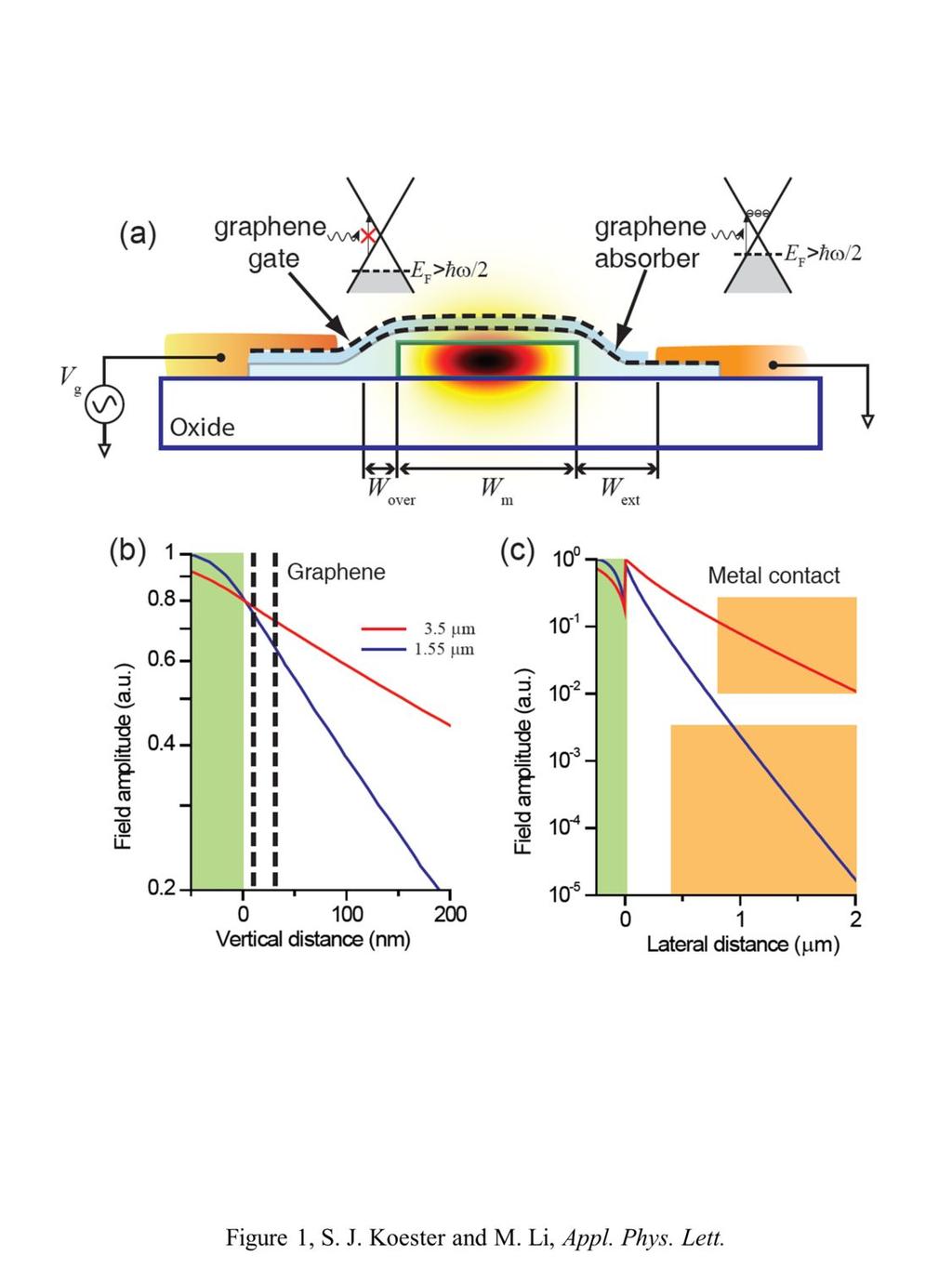
3 and mid-infrared optical signals. Instead of using the doped silicon waveguide as the gate electrode, we propose to use a second layer of graphene which acts as a transparent gate electrode that modulates absorption in the lower graphene layer. This design approach can significantly improve the modulator speed, reduce the insertion loss and simplify the device design. The modulator can be fabricated by transferring two layers of CVD-grown graphene 12 on planar single-mode photonic waveguides, as shown in Fig. 1. The first layer of graphene is transferred to form the bottom absorbing layer. To prevent cracking of the graphene at the edge of the waveguide, the substrate can be planarized by depositing an oxide cladding layer using plasma-enhanced chemical vapor deposition (PECVD) or atomic layer deposition (ALD). As shown in the figure, this layer can also provide a spacer between the lower graphene and the top of the waveguide with a thickness of t bot. The graphene layer can then be patterned and metal can be deposited to form Ohmic contacts. Similarly, a second layer of graphene which acts as the transparent gate electrode can be transferred after deposition of another oxide layer with thickness of t top and contacts can be formed in a similar fashion to the lower layer. A standard silicon-oninsulator (SOI) substrate can be used to fabricate the waveguide layer for use in a spectral range from λ = 1.1 μm to mid-infrared with wavelength up to 3.6 μm. At λ > 3.6 μm the absorption loss in silicon dioxide becomes significant, and therefore, other types of substrates and waveguide structures, such as a suspended silicon membrane, germaniumon-silicon 13 and chalcogenide glasses could be utilized. In the current work, we focus on two specific wavelengths, λ = 1.55 μm and 3.5 μm using an SOI substrate. Page 3 of 15
4 The field amplitude profile in the vertical direction of the waveguide mode is shown in Fig. 1(b). Both the bottom and top graphene layers reside in the evanescent field of the guided optical mode, and the field decay length, L z, is calculated to be 136 nm and 325 nm, for λ = 1.55 μm and 3.5 μm, respectively. For the modulator to operate properly, however, optical absorption should only be allowed in the bottom layer while the top layer should be transparent at the working wavelength. This situation can be achieved if the background carrier concentration, n b, is within a specified range, and if a DC offset voltage, V DC, is applied. Specifically, if the device is tuned such that the bottom-layer Fermi level (relative to the Dirac point) is positioned at /2 while in the top-layer, /2, then proper modulator operation is obtained. 10 Here, is the photon energy. At this condition, 3 the absorption coefficient of graphene is measured to be around 0.09 db/μm at λ = 1.55 μm and is expected to be the same for λ = 3.5 μm. 8 The modulator performance was simulated using an equivalent circuit model taking into account Fermi-Dirac statistics, quantum capacitance effects, and random potential fluctuations in the graphene. The details of this model are included in the supplemental material, 14 and the main features are summarized below. In this model, the unit graphene electron and hole concentrations were determined by integrating the Fermi- Dirac distribution function with the graphene density of states where a random potential, δv i, assumed to have a Gaussian distribution with mean value of 0 and standard deviation of σ, was added to the graphene band structure. A parameter that we call the absorption probability, P i, was defined and can be expressed as P i ( ω 2 E + eδv ) [ 1 f ( ω E + eδv )] = f 2, (1) F i F i Page 4 of 15
5 where f(e) is the Fermi-Dirac distribution function. The average electron and hole sheet densities, n and p, as well as the average absorption probability, P, were then obtained by averaging over m = 1000 random values of δv i. The quantum capacitance, C Q, per unit area was calculated from the derivative of the charge concentration with respect to the Fermi-level position. The procedure above was used to calculate the dependence of C Q, n, p, P on E F and the results were tabulated for given values of temperature, T, and σ. For the grapheneon-graphene modulator geometry, the total modulator capacitance, C m, was then calculated as the series combination of the oxide capacitance, C ox, and the quantum capacitances of the top and bottom graphene layers, where C ox was calculated using a simple parallel plate approximation with an area, A L ( W + 2W ) = as determined from Fig. 1. The gate-voltage dependence of the sheet carrier densities in the bottom and top graphene layers was calculated by assuming a fixed background electron concentration, n b, plus the gate-voltage induced charge calculated by integrating C m over the applied gate voltage. The total series resistance, R m, was calculated by adding the Ohmic resistances of the top and bottom graphene layers as well as the resistance, R c, of the metal contacts to the graphene layers. The mobility, μ, in the graphene layers was assumed to be equal for electrons and holes and was further assumed to be invariant with carrier concentration. 15 The modulator simulations were performed assuming a gate voltage applied to the top graphene layer, with the bottom graphene grounded. The gate voltage consisted of a DC m m over Page 5 of 15
6 offset voltage, V DC plus a sinusoidal AC voltage with peak-to-peak amplitude of V osc. For all simulations, the DC bias voltage was optimized such that when V g = V DC, then /2. The 3dB bandwidth, f 3dB, was calculated from the average value of the RC time constant, τ RC = R m C m, over one complete AC voltage cycle. The absorption in both the top and bottom graphene layers was calculated as the product of the zero-distance absorption coefficient, α 0, the vertical decay of the evanescent optical field, and the absorption probability. Therefore, the total absorption coefficient for the bi-layer structure is simply the sum of the absorption in the bottom and top graphene layers: t ( ) bot / L t z bot + ttop / Lz α = α 0 [ Pbot e + Ptope ]. (2) The relation in (2) corresponds to the total absorption coefficient in the device due to interband absorption, and this value is modulated through the gate voltage-dependence of the absorption probabilities P bot and P top. In addition to band-to-band absorption, absorption by the metal contacts was also accounted for by including an additional linear absorption coefficient, α m, so that the total transmission for the length of the modulator can be expressed as T ( α +α m ) L m = e. From this relation, the insertion loss, L, and modulation depth, M, can be calculated as: L = log( T ), (3) 10 max M T T T max min =, (4) max where T max and T min are the maximum and minimum optical transmission values encountered over the course of one complete AC voltage cycle. Page 6 of 15
7 Table I summarizes the design parameters of the modulators for λ = 1.55 μm and 3.5 μm. The distance between the metal contacts and the waveguide was chosen to be a compromise between metal absorption which increases insertion loss and series resistance in the extension regions which reduces bandwidth (Fig. 1c). A conservative overhang width of 0.15 μm for the graphene on the opposite side of the waveguide was chosen, though this value could be reduced further with high resolution lithography. The values chosen for the mobility and contact resistance, while relatively optimistic for typical CVD graphene values, are still conservative relative to the best values reported in the literature for CVD graphene. 16,17 Finally, a peak-to-peak oscillator voltage of 8 V (3.5 V) was chosen for operation at λ = 1.55 μm (3.5 μm). The simulation results are shown in Fig. 2. The values of L, M and f 3dB are plotted vs. n b for λ = 1.55 μm and 3.5 μm. For all simulations, n b was assumed to be the same for the top and bottom graphene layers. In addition, the results are plotted both for pristine graphene (σ = 0) and for graphene with a realistic value of potential variations (σ = 65 mv). 18 The data in Fig. 2 reveals several interesting trends. First, the modulation depth (Fig. 2(a)) depends strongly on the value of n b. At λ = 1.55 μm, values of M > 0.5 can be achieved for most background concentrations, except for cm -2 < n b < cm -2, where M can be as low as 0.1. This behavior is due primarily to absorption in the top graphene layer as will be explained in more detail below. At λ = 3.5 μm, the modulation performance improves, with M > 0.5, except over a narrow range of n b. Pristine graphene offers somewhat improved modulation depth compared to Page 7 of 15
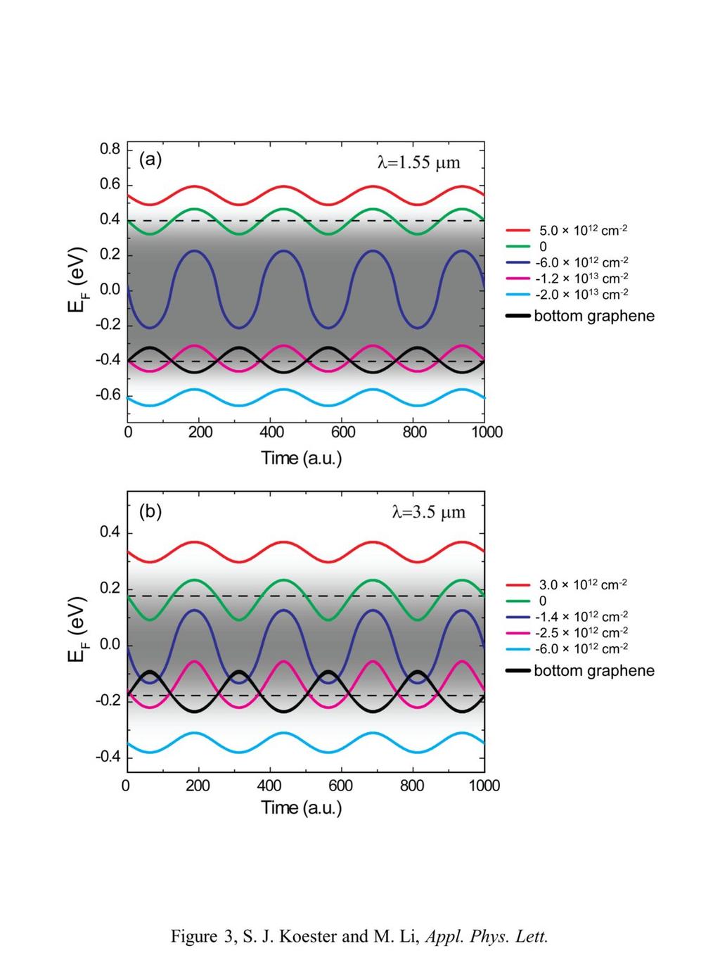
8 disordered graphene. The insertion loss plotted in Fig. 2(b) shows similar behavior to the modulation depth, where at λ = 1.55 μm, significant loss occurs due to absorption in the top graphene layer over a range of n b values, a window that narrows considerably at λ = 3.5 μm. Nevertheless, acceptable insertion loss values around -2.5 db are possible at both wavelengths. Though not shown in the figure, improved insertion loss and modulation depth can be achieved by increasing the peak-to-peak gate voltage swing, primarily at the expense of increased power consumption. Finally, the 3-dB bandwidth, f 3dB is plotted in Fig. 2(c). The plot shows that bandwidths as high as 120 GHz are possible for n-type or strong p-type doping. At λ = 1.55 μm, a bandwidth dip for moderate values of n b occurs when the carrier concentration in the top graphene is at a minimum. The bandwidth at λ = 3.5 μm is roughly 3 times lower than at λ = 1.55 μm primarily due to the larger lateral dimensions of the waveguide and lower carrier concentrations which increase both R m and C m compared to shorter wavelengths. In order to better understand the behavior of the results in Fig. 2, the time-dependent Fermi-level energies in the top ( ) and bottom ( ) graphene layers, for specific values of n b, have been plotted in Fig. 3. In these calculations, the modulator is assumed to be operating at a frequency well below f 3dB. For each curve, the DC offset voltage has been chosen such that /2 when V g = V DC. The absorption probability P is depicted in the plot by the shaded background. For both λ = 1.55 μm and λ = 3.5 μm, when the graphene is doped n-type (red lines) or strongly p-type (cyan Page 8 of 15
9 lines), the Fermi-level in the top graphene remains in a region of low absorption. The peak in the modulation depth (Fig. 2a) occurs when n b = 0, corresponding to the situation where a gate voltage change makes both the top and bottom graphene layers more or less absorbing at the same time (green lines). Conversely, the poorest modulation depth occurs when the starting Fermi-level positions in the top and bottom graphene layers are the same (magenta lines). In this case, the absorption modulation in the bottom layer is counteracted by the opposite effect in the top layer. A summary of the device performance for a selection of operational parameters is shown in Table 2. At λ = 1.55 μm, provided very strong p-type doping of 1.8 x cm -2 can be realized, 19 a bandwidth of 120 GHz, modulation depth > 0.5 and insertion loss of -2.5 db can be achieved at V osc = 8 V. At λ = 3.5 μm, the required background hole concentration for optimal operation is reduced to ~ 6.5 x cm -2 (which is close to the natural p-type doping that occurs in transferred CVD graphene layers). 20 Furthermore, good modulation depth of 0.55 and -2.5 db insertion loss can be obtained. However, the larger dimensions of the devices at λ = 3.5 μm restrict the bandwidth to ~ 30 GHz. The results above provide the basic guidelines for design of graphene-on-graphene electroabsorption optical modulators. However, they do not necessarily predict the ultimate performance capabilities, and improvements in the device design are possible. Since the device operation is limited by RC delays, the utilization of double-sided contacts on the top and bottom graphene layers could improve the bandwidth by reducing the series resistance by nearly a factor of two. If the top graphene background concentration could be controlled independent of the bottom layer, further reduction of Page 9 of 15
10 the series resistance could be achieved, while at the same time reducing the required value of the DC offset. The use of multi-layer graphene for the top contact could further reduce parasitic series resistance. Improvements in the simulations, including using a distributed RC model, accounting for the effect of disorder on mobility, and consideration of the effect of the graphene on the optical mode 21 could lead to more accurate predictions of the device performance. In conclusion, an SOI-waveguide-coupled double-layer graphene modulator concept has been described. Bandwidths over 120 GHz (30 GHz) are predicted for a single-ended contact design at λ = 1.55 μm (3.5 μm). The effect of background doping and potential fluctuations on the bandwidth, modulation depth and insertion loss have been quantified and suggestions for future design improvements have been provided. Page 10 of 15
11 References 1 2 F. Bonaccorso, Z. Sun, T. Hasan, and A. C. Ferrari, Nature Photonics 4, 611 (2010). F. Xia, T. Mueller, Y. M. Lin, A. Valdes-Garcia, and Ph. Avouris, Nature Nanotech. 4, 839 (2009). 3 M. Liu, X. Yin, E. Ulin-Avila, B. Geng, T. Zentgraf, L. Ju, F. Wang, X. Zhang, Nature 474, 64 (2011). 4 Q. Bao, H. Zhang, B. Wang, Z. Ni, C. Haley, Y. X. Lim, Y. Wang, D. Y. Tang, and K. P. Loh, Nature Photonics 5, 411 (2011) M. Jablan, H. Buljan, and M. Soljačić, Phys. Rev. B 80, (2009). F. H. Koppens, D. E. Chang, and F. J. Garcia de Abajo, Nano Lett. 11, 3370 (2011). A. Vakil and N. Engheta, Science 332, 1291 (2011). A. Kuzmenko, E. van Heumen, F. Carbone, and D. van der Marel, Phys. Rev. Lett. 100, (2008). 9 R. R. Nair, P. Blake, A. N. Grigorenko, K. S. Novoselov, T. J. Booth, T. Stauber, N. M. R. Peres and A. K. Geim, Science 320, 1308 (2008). 10 F. Wang, Y. Zhang, C. Tian, C. Girit, A. Zettl, M. Crommie, and Y. R. Shen, Science 320, 206 (2008). 11 Q. Li, E. A. Henriksen, Z. Jiang, Z. Hao, M. C. Martin, P. Kim, H. L. Stormer, and D. N. Basov, Nature Physics 4, 532 (2008). 12 X. Li, W. Cai, J. An, S. Kim, J. Nah, D. Yang, R. Piner, A. Velamakanni, I. Jung, E. Tutuc, S. K. Banerjee, L. Colombo, and R. S. Ruoff, Science 324, 1312 (2009). Page 11 of 15
12 13 R. A. Soref, S. J. Emelett, and W. R. Buchwald, J. Opt. A, Pure Appl. Opt. 8, 840 (2006) See supplementary material for details of theoretical modeling. A. Venugopal, J. Chan, X. Li, C. W. Magnuson, W. P. Kirk, L. Colombo, R. S. Ruoff, and E. M. Vogel, J. Appl. Phys. 109, (2011). 16 X. Li, C. W. Magnuson, A. Venugopal, J. An, J. W. Suk, B. Han, M. Borysiak, W. Cai, A. Velamakanni, Y. Zhu, L. Fu, E. M. Vogel, E. Voelkl, L. Colombo, and R. S. Ruoff, Nano Lett. 10, 4328 (2010). 17 A. D. Franklin, S.-J. Han, A. A. Bol, and V. Perebeinos, IEEE Elect. Dev. Lett. 33, 17 (2012) M. A. Ebrish, H. Shao and S. J. Koester, submitted to Appl. Phys. Lett.. H.-J. Shin, W. M. Choi, D. Choi, G. H. Han, S.-M. Yoon, H.-K. Park, S.-W. Kim, Y. W. Jin, S. Y. Lee, J. M. Kim, J.-Y. Choi, and Y. H. Lee, J. Am. Chem. Soc. 132, (2010) O. M. Nayfeh, IEEE Trans. Elect. Dev. 58, 2847 (2011). S. Mikhailov and K. Ziegler, Phys. Rev. Lett. 99, (2007). Page 12 of 15
13 TABLE I. NOMINAL GRAPHENE MODULATOR VALUES USED FOR SIMULATIONS. Symbol Parameter Default Value λ Waveglength 1.55 μm (3.5 μm) L m Modulator length 60 μm W m Waveguide width 0.5 μm (1.0 μm) W ext Extension width 0.4 μm (0.8 μm) W over Overlap width 0.15 μm t top Top oxide thickness 20 nm ε top Top oxide dielectric constant 3.9 t bot Bottom oxide thickness 10 nm ε bot Botom oxide dielectric constant 3.9 σ Random potential fluctuations 0 and 65 mv μ Mobility (both e and h) 4000 cm 2 /Vs R c Contact resistance 400 Ω-μm T Temperature 300 K α 0 Zero-distance absorption coefficient μm -1 V osc Peak-to-peak AC voltage 8 V (3.5 V) Page 13 of 15
14 TABLE II. PERFORMANCE SUMMARY OF GRAPHENE MODULATORS. Symbol Value at λ = 1.55 μm Value at λ = 3.5 μm V osc 8 V 3.5 V n b -1.8 x cm x cm -2 V DC +5.5 V +3.7 V f 3dB 121 GHz 31.8 GHz M L -2.5 db -2.5 db Page 14 of 15
15 Figure Captions Figure 1. (a) Structure of the proposed dual-layer graphene modulator integrated on a waveguide. Overlay shows mode profile of the waveguide s fundamental TE mode. (b) Vertical direction profile of the electric field component amplitude decaying from the top surface of the waveguide. Green shaded area marks the waveguie. Dashed lines mark the graphene layers. (c) Lateral direction profile of the electric field component amplitude decaying from the side surface of the waveguide. Yellow shaded area marks the metal contact. Figure 2. Plot of (a) modulation depth, (b) insertion loss and (c) bandwidth vs. background electron conentration, n b, for waveguide-coupled graphene-on-graphene optical modulator using the device parameters listed in Table 1. The graphs are shown for both λ = 1.55 μm (blue) and λ = 3.5 μm (red), and for pristine graphene with σ = 0 (dashed lines) as well as graphene with random potential fluctuations of σ = 65 mv (solid lines). The circles represent the optimal design points listed in Table II. Figure 3. Plot of Fermi level vs. time for top (colors) and bottom (black) graphene layers for several fixed values of n b listed on the right side of the graphs. In (a), λ = 1.55 μm, while in (b), λ = 3.5 μm. For both (a) and (b), graphene layers with realistic potential fluctuations of σ = 65 mv have been utilized. Page 15 of 15
16
17
18
Controlling Graphene Ultrafast Hot Carrier Response from Metal-like. to Semiconductor-like by Electrostatic Gating
 Controlling Graphene Ultrafast Hot Carrier Response from Metal-like to Semiconductor-like by Electrostatic Gating S.-F. Shi, 1,2* T.-T. Tang, 1 B. Zeng, 1 L. Ju, 1 Q. Zhou, 1 A. Zettl, 1,2,3 F. Wang 1,2,3
Waveguide-Coupled Graphene Optoelectronics
 > REPLACE THIS LINE WITH YOUR PAPER IDENTIFICATION NUMBER (DOUBLE-CLICK HERE TO EDIT) < 1 Waveguide-Coupled Graphene Optoelectronics Steven J. Koester, Senior Member, IEEE, and Mo Li, Member, IEEE Abstract
Hybrid Surface-Phonon-Plasmon Polariton Modes in Graphene /
 Supplementary Information: Hybrid Surface-Phonon-Plasmon Polariton Modes in Graphene / Monolayer h-bn stacks Victor W. Brar 1,2, Min Seok Jang 3,, Michelle Sherrott 1, Seyoon Kim 1, Josue J. Lopez 1, Laura
Highly Confined Tunable Mid-Infrared Plasmonics in Graphene Nanoresonators
 Supplementary Information for Highly Confined Tunable Mid-Infrared Plasmonics in Graphene Nanoresonators by Victor W. Brar, Min Seok Jang, Michelle Sherrott, Josue J. Lopez and Harry Atwater 1 Approximating
Wafer-Scale Single-Domain-Like Graphene by. Defect-Selective Atomic Layer Deposition of
 Electronic Supplementary Material (ESI) for Nanoscale. This journal is The Royal Society of Chemistry 2015 Wafer-Scale Single-Domain-Like Graphene by Defect-Selective Atomic Layer Deposition of Hexagonal
photonic crystals School of Space Science and Physics, Shandong University at Weihai, Weihai , China
 Enhanced absorption in heterostructures with graphene and truncated photonic crystals Yiping Liu 1, Lei Du 1, Yunyun Dai 2, Yuyu Xia 2, Guiqiang Du 1,* Guang Lu 1, Fen Liu 1, Lei Shi 2, Jian Zi 2 1 School
Graphene photodetectors with ultra-broadband and high responsivity at room temperature
 SUPPLEMENTARY INFORMATION DOI: 10.1038/NNANO.2014.31 Graphene photodetectors with ultra-broadband and high responsivity at room temperature Chang-Hua Liu 1, You-Chia Chang 2, Ted Norris 1.2* and Zhaohui
Surface-normal electro-optic spatial light modulator using graphene integrated on a high-contrast grating resonator
 Vol. 24, No. 23 14 Nov 2016 OPTICS EXPRESS 26035 Surface-normal electro-optic spatial light modulator using graphene integrated on a high-contrast grating resonator TIANBO SUN,1,6 JONGHWAN KIM,2,6 JONG
Tunable graphene-based polarizer
 Tunable graphene-based polarizer Yu. V. Bludov, 1, a) M. I. Vasilevskiy, 1 and N. M. R. Peres 1 Centro de Física & Departamento de Física, Universidade do Minho, Campus de Gualtar, Braga 4710-057, Portugal
Graphene-based long-wave infrared TM surface plasmon modulator
 Graphene-based long-wave infrared TM surface plasmon modulator David R. Andersen 1, 1 Department of Electrical and Computer Engineering, Department of Physics and Astronomy, The University of Iowa, Iowa
Supplementary Information
 Supplementary Information Plasma-assisted reduction of graphene oxide at low temperature and atmospheric pressure for flexible conductor applications Seung Whan Lee 1, Cecilia Mattevi 2, Manish Chhowalla
Multilayer graphene under vertical electric field
 Multilayer graphene under vertical electric field S. Bala kumar and Jing Guo a) Department of Electrical and Computer Engineering, University of Florida, Gainesville, Florida 3608, USA Abstract We study
Nanoscale Graphene Electro-Optic Modulators
 Nanoscale Graphene Electro-Optic Modulators Zhaolin Lu* and Wangshi Zhao Microsystems Engineering, Kate Gleason College of Engineering, Rochester Institute of Technology, Rochester, New York, 14623, USA
Supplementary material for High responsivity mid-infrared graphene detectors with antenna-enhanced photo-carrier generation and collection
 Supplementary material for High responsivity mid-infrared graphene detectors with antenna-enhanced photo-carrier generation and collection Yu Yao 1, Raji Shankar 1, Patrick Rauter 1, Yi Song 2, Jing Kong
Drift-diffusion model for single layer transition metal dichalcogenide field-effect transistors
 Drift-diffusion model for single layer transition metal dichalcogenide field-effect transistors David Jiménez Departament d'enginyeria Electrònica, Escola d'enginyeria, Universitat Autònoma de Barcelona,
Ultrafast Lateral Photo-Dember Effect in Graphene. Induced by Nonequilibrium Hot Carrier Dynamics
 1 Ultrafast Lateral Photo-Dember Effect in Graphene Induced by Nonequilibrium Hot Carrier Dynamics Chang-Hua Liu, You-Chia Chang, Seunghyun Lee, Yaozhong Zhang, Yafei Zhang, Theodore B. Norris,*,, and
crystals were phase-pure as determined by x-ray diffraction. Atomically thin MoS 2 flakes were
 Nano Letters (214) Supplementary Information for High Mobility WSe 2 p- and n-type Field Effect Transistors Contacted by Highly Doped Graphene for Low-Resistance Contacts Hsun-Jen Chuang, Xuebin Tan, Nirmal
Graphene-polymer multilayer heterostructure for terahertz metamaterials
 University of Wollongong Research Online Faculty of Engineering and Information Sciences - Papers: Part A Faculty of Engineering and Information Sciences 2013 Graphene-polymer multilayer heterostructure
Black phosphorus: A new bandgap tuning knob
 Black phosphorus: A new bandgap tuning knob Rafael Roldán and Andres Castellanos-Gomez Modern electronics rely on devices whose functionality can be adjusted by the end-user with an external knob. A new
graphene nano-optoelectronics Frank Koppens ICFO, The institute of photonic sciences, Barcelona
 graphene nano-optoelectronics Frank Koppens ICFO, The institute of photonic sciences, Barcelona Graphene research at ICFO Frank Koppens: group Nano-optoelectronics (~100% graphene) Nano-optics and plasmonics
GHZ ELECTRICAL PROPERTIES OF CARBON NANOTUBES ON SILICON DIOXIDE MICRO BRIDGES
 GHZ ELECTRICAL PROPERTIES OF CARBON NANOTUBES ON SILICON DIOXIDE MICRO BRIDGES SHENG F. YEN 1, HAROON LAIS 1, ZHEN YU 1, SHENGDONG LI 1, WILLIAM C. TANG 1,2, AND PETER J. BURKE 1,2 1 Electrical Engineering
Linear and Nonlinear Microwave Characterization of CVD- Grown Graphene Using CPW Structure
 Linear and Nonlinear Microwave Characterization of CVD- Grown Graphene Using CPW Structure Mingguang Tuo 1, Si Li 1,2, Dongchao Xu 3, Min Liang 1, Qi Zhu 2, Qing Hao 3, Hao Xin 1 1 Department of Electrical
Efficient Preparation of Large-Area Graphene Oxide Sheets for Transparent Conductive Films
 Supporting Information Efficient Preparation of Large-Area Graphene Oxide Sheets for Transparent Conductive Films Jinping Zhao, Songfeng Pei, Wencai Ren*, Libo Gao and Hui-Ming Cheng* Shenyang National
Ambipolar bistable switching effect of graphene
 Ambipolar bistable switching effect of graphene Young Jun Shin, 1,2 Jae Hyun Kwon, 1,2 Gopinadhan Kalon, 1,2 Kai-Tak Lam, 1 Charanjit S. Bhatia, 1 Gengchiau Liang, 1 and Hyunsoo Yang 1,2,a) 1 Department
SUPPLEMENTARY INFORMATION
 SUPPLEMENTARY INFORMATION SUPPLEMENTARY INFORMATION Trilayer graphene is a semimetal with a gate-tuneable band overlap M. F. Craciun, S. Russo, M. Yamamoto, J. B. Oostinga, A. F. Morpurgo and S. Tarucha
Highly Sensitive and Wide-Band Tunable Terahertz Response of Plasma Wave based on Graphene Field Effect Transistors
 Supplementary Information Highly Sensitive and Wide-Band Tunable Terahertz Response of Plasma Wave based on Graphene Field Effect Transistors Lin Wang, Xiaoshuang Chen *, Anqi Yu, Yang Zhang, Jiayi Ding
(a) (b) Supplementary Figure 1. (a) (b) (a) Supplementary Figure 2. (a) (b) (c) (d) (e)
 (b) Supplementary Figure 1. (a) (b) (a) Supplementary Figure 2. (a) (b) (c) (d) (e)") (a) (b) Supplementary Figure 1. (a) An AFM image of the device after the formation of the contact electrodes and the top gate dielectric Al 2 O 3. (b) A line scan performed along the white dashed line
(a) (b) Supplementary Figure 1. (a) An AFM image of the device after the formation of the contact electrodes and the top gate dielectric Al 2 O 3. (b) A line scan performed along the white dashed line
AN IMPROVED METHOD FOR TRANSFERRING GRAPHENE GROWN BY CHEMICAL VAPOR DEPOSITION
 NANO: Brief Reports and Reviews Vol. 7, No. 1 (2012) 1150001 (6 pages) World Scienti c Publishing Company DOI: 10.1142/S1793292011500019 AN IMPROVED METHOD FOR TRANSFERRING GRAPHENE GROWN BY CHEMICAL VAPOR
Graphene Chemical Vapor Deposition (CVD) Growth
 Growth") ECE440 Nanoelectronics Graphene Chemical Vapor Deposition (CVD) Growth Zheng Yang Timeline of graphene CVD growth Exfoliation
ECE440 Nanoelectronics Graphene Chemical Vapor Deposition (CVD) Growth Zheng Yang Timeline of graphene CVD growth Exfoliation
Graphene Varactors as a Sensing Platform for Biotechnology Applications
 Graphene Varactors as a Sensing Platform for Biotechnology Applications Steven J. Koester 1, Eric J. Olson 1, David Deen 1, Yao Zhang 1, Mona A. Ebrish 1, Rui Ma 1, Nazila Haratipour 1, Philippe Buhlmann
Ag-mesh-combined graphene for an indium-free current spreading layer in near-ultraviolet light-emitting diodes
 Ag-mesh-combined graphene for an indium-free current spreading layer in near-ultraviolet light-emitting diodes Journal: RSC Advances Manuscript ID: RA-ART-06-2015-012642.R1 Article Type: Paper Date Submitted
Supporting Information for: Electrical probing and tuning of molecular. physisorption on graphene
 Supporting Information for: Electrical probing and tuning of molecular physisorption on graphene Girish S. Kulkarni, Karthik Reddy #, Wenzhe Zang, Kyunghoon Lee, Xudong Fan *, and Zhaohui Zhong * Department
ULTRA-SHORT OPTICAL PULSE GENERATION WITH SINGLE-LAYER GRAPHENE
 Journal of Nonlinear Optical Physics & Materials Vol. 19, No. 4 (2010) 767 771 c World Scientific Publishing Company DOI: 10.1142/S021886351000573X ULTRA-SHORT OPTICAL PULSE GENERATION WITH SINGLE-LAYER
Graphene Modulators and Switches Integrated on Silicon and Silicon Nitride Waveguide
 > REPLACE THIS LINE WITH YOUR PAPER IDENTIFICATION NUMBER (DOUBLE-CLICK HERE TO EDIT) < 1 Graphene Modulators and Switches Integrated on Silicon and Silicon Nitride Waveguide Leili. A. Shiramin, Dries.
Superconductivity Induced Transparency
 Superconductivity Induced Transparency Coskun Kocabas In this paper I will discuss the effect of the superconducting phase transition on the optical properties of the superconductors. Firstly I will give
Ge Quantum Well Modulators on Si. D. A. B. Miller, R. K. Schaevitz, J. E. Roth, Shen Ren, and Onur Fidaner
 10.1149/1.2986844 The Electrochemical Society Ge Quantum Well Modulators on Si D. A. B. Miller, R. K. Schaevitz, J. E. Roth, Shen Ren, and Onur Fidaner Ginzton Laboratory, 450 Via Palou, Stanford CA 94305-4088,
Transport Properties of Graphene Nanoribbon Transistors on. Chemical-Vapor-Deposition Grown Wafer-Scale Graphene
 Transport Properties of Graphene Nanoribbon Transistors on Chemical-Vapor-Deposition Grown Wafer-Scale Graphene Wan Sik Hwang 1, a), Kristof Tahy 1, Xuesong Li 2, Huili (Grace) Xing 1, Alan C. Seabaugh
Theoretical Study on Graphene Silicon Heterojunction Solar Cell
 Copyright 2015 American Scientific Publishers All rights reserved Printed in the United States of America Journal of Nanoelectronics and Optoelectronics Vol. 10, 1 5, 2015 Theoretical Study on Graphene
Highly Efficient Graphene-Based Optical Modulator With Edge Plasmonic Effect
 Highly Efficient Graphene-Based Optical Modulator With Edge Plasmonic Effect Ran Hao, Ziwei Ye, Xiliang Peng, Yijie Gu, JianYao Jiao, Haixia Zhu, Wei E. I. Sha, and Erping Li Key Laboratory of Advanced
SUPPLEMENTARY INFORMATION
 SUPPLEMENTARY INFORMATION Flexible, high-performance carbon nanotube integrated circuits Dong-ming Sun, Marina Y. Timmermans, Ying Tian, Albert G. Nasibulin, Esko I. Kauppinen, Shigeru Kishimoto, Takashi
Supplemental Materials
 Supplemental Materials On the modeling of graphene layer by a thin dielectric Modeling graphene as a D surface having an appropriate value of surface conductivity σ is an accurate approach for a semiclassical
A Broadband Flexible Metamaterial Absorber Based on Double Resonance
 Progress In Electromagnetics Research Letters, Vol. 46, 73 78, 2014 A Broadband Flexible Metamaterial Absorber Based on Double Resonance ong-min Lee* Abstract We present a broadband microwave metamaterial
Supplementary Information for. Vibrational Spectroscopy at Electrolyte Electrode Interfaces with Graphene Gratings
 Supplementary Information for Vibrational Spectroscopy at Electrolyte Electrode Interfaces with Graphene Gratings Supplementary Figure 1. Simulated from pristine graphene gratings at different Fermi energy
Polarization dependence of photocurrent in a metalgraphene-metal
 Polarization dependence of photocurrent in a metalgraphene-metal device Minjung Kim, 1 Ho Ang Yoon, 2 Seungwoo Woo, 1 Duhee Yoon, 1 Sang Wook Lee, 2 and Hyeonsik Cheong 1,a) 1 Department of Physics, Sogang
MICROWAVE AND MILLIMETERWAVE ELECTRICAL PERMITTIVITY OF GRAPHENE MONOLAYER. G. Konstantinidis 3
 1 MICROWAVE AND MILLIMETERWAVE ELECTRICAL PERMITTIVITY OF GRAPHENE MONOLAYER Alina Cismaru 1, Mircea Dragoman 1*, Adrian Dinescu 1, Daniela Dragoman 2, G. Stavrinidis, G. Konstantinidis 3 1 National Institute
Bends and splitters in graphene nanoribbon waveguides
 Downloaded from orbit.dtu.dk on: Dec 20, 2017 Bends and splitters in graphene nanoribbon waveguides Zhu, Xiaolong; Yan, Wei; Mortensen, N. Asger; Xiao, Sanshui Published in: Optics Express Link to article,
SUPPLEMENTARY INFORMATION
 Dirac electron states formed at the heterointerface between a topological insulator and a conventional semiconductor 1. Surface morphology of InP substrate and the device Figure S1(a) shows a 10-μm-square
Solvothermal Reduction of Chemically Exfoliated Graphene Sheets
 Solvothermal Reduction of Chemically Exfoliated Graphene Sheets Hailiang Wang, Joshua Tucker Robinson, Xiaolin Li, and Hongjie Dai* Department of Chemistry and Laboratory for Advanced Materials, Stanford
Supplementary Figure S1. AFM images of GraNRs grown with standard growth process. Each of these pictures show GraNRs prepared independently,
 Supplementary Figure S1. AFM images of GraNRs grown with standard growth process. Each of these pictures show GraNRs prepared independently, suggesting that the results is reproducible. Supplementary Figure
Engineering Product Development, Singapore University of Technology and Design, 20 Dover Drive, Singapore
 Waveguide Engineering of Graphene s Nonlinearity Kelvin J. A. Ooi, Lay Kee Ang and Dawn T. H. Tan* Engineering Product Development, Singapore University of Technology and Design, 0 Dover Drive, Singapore
arxiv: v1 [physics.optics] 6 Jul 2018
![arxiv: v1 [physics.optics] 6 Jul 2018](/thumbs/81/84537555.jpg "arxiv: v1 [physics.optics] 6 Jul 2018") arxiv:1807.02240v1 [physics.optics] 6 Jul 2018 Independently tunable dual-spectral electromagnetically induced transparency in a terahertz metal-graphene metamaterial Tingting Liu 1, Huaixing Wang 1, Yong
arxiv:1807.02240v1 [physics.optics] 6 Jul 2018 Independently tunable dual-spectral electromagnetically induced transparency in a terahertz metal-graphene metamaterial Tingting Liu 1, Huaixing Wang 1, Yong
Supporting Online Material for
 www.sciencemag.org/cgi/content/full/327/5966/662/dc Supporting Online Material for 00-GHz Transistors from Wafer-Scale Epitaxial Graphene Y.-M. Lin,* C. Dimitrakopoulos, K. A. Jenkins, D. B. Farmer, H.-Y.
Supplementary Information. Experimental Evidence of Exciton Capture by Mid-Gap Defects in CVD. Grown Monolayer MoSe2
 Supplementary Information Experimental Evidence of Exciton Capture by Mid-Gap Defects in CVD Grown Monolayer MoSe2 Ke Chen 1, Rudresh Ghosh 2,3, Xianghai Meng 1, Anupam Roy 2,3, Joon-Seok Kim 2,3, Feng
Supplementary Figure 1 Magneto-transmission spectra of graphene/h-bn sample 2 and Landau level transition energies of three other samples.
 Supplementary Figure 1 Magneto-transmission spectra of graphene/h-bn sample 2 and Landau level transition energies of three other samples. (a,b) Magneto-transmission ratio spectra T(B)/T(B 0 ) of graphene/h-bn
Wafer Scale Homogeneous Bilayer Graphene Films by. Chemical Vapor Deposition
 Supporting Information for Wafer Scale Homogeneous Bilayer Graphene Films by Chemical Vapor Deposition Seunghyun Lee, Kyunghoon Lee, Zhaohui Zhong Department of Electrical Engineering and Computer Science,
Some more detailed remarks: 1) Explain how the geometry of the slow light PhC cavity is selected. Is it an optimized version?
 Explain how the geometry of the slow light PhC cavity is selected. Is it an optimized version?") Reviewers' Comments: Reviewer #1 (Remarks to the Author) Graphene-based microheaters with the combination of slow-light effect in silicon photonic crystal waveguides are utilized to enhance the heating
Reviewers' Comments: Reviewer #1 (Remarks to the Author) Graphene-based microheaters with the combination of slow-light effect in silicon photonic crystal waveguides are utilized to enhance the heating
The role of charge traps in inducing hysteresis: capacitance voltage measurements on top gated bilayer graphene
 The role of charge traps in inducing hysteresis: capacitance voltage measurements on top gated bilayer graphene Gopinadhan Kalon, Young Jun Shin, Viet Giang Truong, Alan Kalitsov, and Hyunsoo Yang a) Department
Supporting Online Material for
 www.sciencemag.org/cgi/content/full/320/5874/356/dc1 Supporting Online Material for Chaotic Dirac Billiard in Graphene Quantum Dots L. A. Ponomarenko, F. Schedin, M. I. Katsnelson, R. Yang, E. W. Hill,
Supporting Information
 Copyright WILEY-VCH Verlag GmbH & Co. KGaA, 69469 Weinheim, Germany, 213. Supporting Information for Adv. Mater., DOI: 1.12/adma.2134949 Large Arrays and Properties of 3-Terminal Graphene Nanoelectromechanical
Graphene-Based Infrared Lens with Tunable Focal Length
 Progress In Electromagnetics Research, Vol. 155, 19 26, 2016 Graphene-Based Infrared Lens with Tunable Focal Length Yan Xiu Li, Fan Min Kong *, and Kang Li Abstract In modern information and communication
SUPPLEMENTARY INFORMATION
 Supplementary Information: Photocurrent generation in semiconducting and metallic carbon nanotubes Maria Barkelid 1*, Val Zwiller 1 1 Kavli Institute of Nanoscience, Delft University of Technology, Delft,
Intrinsic Electronic Transport Properties of High. Information
 Intrinsic Electronic Transport Properties of High Quality and MoS 2 : Supporting Information Britton W. H. Baugher, Hugh O. H. Churchill, Yafang Yang, and Pablo Jarillo-Herrero Department of Physics, Massachusetts
SENSITIVITY ENHANCEMENT OF A D-SHAPE SPR-POF LOW-COST SENSOR USING GRAPHENE
 International Journal of Education and Research Vol. No. November 03 SENSITIVITY ENHANCEMENT OF A D-SHAPE SPR-POF LOW-COST SENSOR USING GRAPHENE Ramona GALATUS, Lorant SZOLGA, Emil VOICULESCU Technical
Fourier Optics on Graphene
 Fourier Optics on Graphene Ashkan Vakil and Nader Engheta * Department of Electrical & Systems Engineering University of Pennsylvania Philadelphia, PA 19104, USA Abstract Using numerical simulations, here
Supplementary Figure 1. Selected area electron diffraction (SAED) of bilayer graphene and tblg. (a) AB
 of bilayer graphene and tblg. (a) AB") Supplementary Figure 1. Selected area electron diffraction (SAED) of bilayer graphene and tblg. (a) AB stacked bilayer graphene (b), (c), (d), (e), and (f) are twisted bilayer graphene with twist angle
Supplementary Figure 1. Selected area electron diffraction (SAED) of bilayer graphene and tblg. (a) AB stacked bilayer graphene (b), (c), (d), (e), and (f) are twisted bilayer graphene with twist angle
UvA-DARE (Digital Academic Repository) Charge carrier dynamics in photovoltaic materials Jensen, S.A. Link to publication
 Charge carrier dynamics in photovoltaic materials Jensen, S.A. Link to publication") UvA-DARE (Digital Academic Repository) Charge carrier dynamics in photovoltaic materials Jensen, S.A. Link to publication Citation for published version (APA): Jensen, S. A. (2014). Charge carrier dynamics
UvA-DARE (Digital Academic Repository) Charge carrier dynamics in photovoltaic materials Jensen, S.A. Link to publication Citation for published version (APA): Jensen, S. A. (2014). Charge carrier dynamics
arxiv: v1 [cond-mat.mes-hall] 9 Mar 2016
![arxiv: v1 [cond-mat.mes-hall] 9 Mar 2016](/thumbs/72/68000826.jpg "arxiv: v1 [cond-mat.mes-hall] 9 Mar 2016") Dynamically controllable graphene three-port arxiv:1603.02936v1 [cond-mat.mes-hall] 9 Mar 2016 circulator Victor Dmitriev, Wagner Castro,, and Clerisson Nascimento Department of Electrical Engineering,
Dynamically controllable graphene three-port arxiv:1603.02936v1 [cond-mat.mes-hall] 9 Mar 2016 circulator Victor Dmitriev, Wagner Castro,, and Clerisson Nascimento Department of Electrical Engineering,
Supporting Information Available:
 Supporting Information Available: Photoresponsive and Gas Sensing Field-Effect Transistors based on Multilayer WS 2 Nanoflakes Nengjie Huo 1, Shengxue Yang 1, Zhongming Wei 2, Shu-Shen Li 1, Jian-Bai Xia
CHAPTER 5 EFFECT OF GATE ELECTRODE WORK FUNCTION VARIATION ON DC AND AC PARAMETERS IN CONVENTIONAL AND JUNCTIONLESS FINFETS
 98 CHAPTER 5 EFFECT OF GATE ELECTRODE WORK FUNCTION VARIATION ON DC AND AC PARAMETERS IN CONVENTIONAL AND JUNCTIONLESS FINFETS In this chapter, the effect of gate electrode work function variation on DC
A Bottom-gate Depletion-mode Nanowire Field Effect Transistor (NWFET) Model Including a Schottky Diode Model
 Model Including a Schottky Diode Model") Journal of the Korean Physical Society, Vol. 55, No. 3, September 2009, pp. 1162 1166 A Bottom-gate Depletion-mode Nanowire Field Effect Transistor (NWFET) Model Including a Schottky Diode Model Y. S.
Journal of the Korean Physical Society, Vol. 55, No. 3, September 2009, pp. 1162 1166 A Bottom-gate Depletion-mode Nanowire Field Effect Transistor (NWFET) Model Including a Schottky Diode Model Y. S.
Electrically Tunable Coherent Optical Absorption in Graphene with Ion Gel
 pubs.acs.org/nanolett Electrically Tunable Coherent Optical Absorption in Graphene with Ion Gel Vrinda Thareja, Ju-Hyung Kang,, Hongtao Yuan,, Kaveh M. Milaninia, Harold Y. Hwang,, Yi Cui,, Pieter G. Kik,,
Supporting Information
 Electronic Supplementary Material (ESI) for Nanoscale. This journal is The Royal Society of Chemistry 215 Supporting Information Enhanced Photovoltaic Performances of Graphene/Si Solar Cells by Insertion
Terahertz (THz) technology, owing to its applications in
 technology, owing to its applications in") pubs.acs.org/nanolett Extraordinary Control of Terahertz Beam Reflectance in Graphene Electro-absorption Modulators Berardi Sensale-Rodriguez,*, Rusen Yan,, Subrina Rafique, Mingda Zhu, Wei Li,, Xuelei
pubs.acs.org/nanolett Extraordinary Control of Terahertz Beam Reflectance in Graphene Electro-absorption Modulators Berardi Sensale-Rodriguez,*, Rusen Yan,, Subrina Rafique, Mingda Zhu, Wei Li,, Xuelei
Nonlinear Control of Absorption in Graphene-based 1D Photonic Crystal
 Nonlinear Control of Absorption in Graphene-based 1D Photonic Crystal M A Vincenti 1,*, D de Ceglia 1, M Grande 2, A D Orazio 2, M Scalora 3 1 National Research Council - AMRDEC, Charles M Bowden Research
Optimum Access Waveguide Width for 1xN Multimode. Interference Couplers on Silicon Nanomembrane
 Optimum Access Waveguide Width for 1xN Multimode Interference Couplers on Silicon Nanomembrane Amir Hosseini 1,*, Harish Subbaraman 2, David Kwong 1, Yang Zhang 1, and Ray T. Chen 1,* 1 Microelectronic
Highly Conductive 3D Nano-Carbon: Stacked Multilayer Graphene System with Interlayer Decoupling
 Highly Conductive 3D Nano-Carbon: Stacked Multilayer Graphene System with Interlayer Decoupling Tianhua Yu, Changdong Kim, and Bin Yu*, College of Nanoscale Science and Engineering, State University of
vapour deposition. Raman peaks of the monolayer sample grown by chemical vapour
 Supplementary Figure 1 Raman spectrum of monolayer MoS 2 grown by chemical vapour deposition. Raman peaks of the monolayer sample grown by chemical vapour deposition (S-CVD) are peak which is at 385 cm
Over the past decade, graphene has been intensively
 pubs.acs.org/journal/apchd5 Terms of Use Total Absorption in a Graphene Monolayer in the Optical Regime by Critical Coupling with a Photonic Crystal Guided Resonance Jessica R. Piper* and Shanhui Fan*
TRANSVERSE SPIN TRANSPORT IN GRAPHENE
 International Journal of Modern Physics B Vol. 23, Nos. 12 & 13 (2009) 2641 2646 World Scientific Publishing Company TRANSVERSE SPIN TRANSPORT IN GRAPHENE TARIQ M. G. MOHIUDDIN, A. A. ZHUKOV, D. C. ELIAS,
Resonator Fabrication for Cavity Enhanced, Tunable Si/Ge Quantum Cascade Detectors
 Resonator Fabrication for Cavity Enhanced, Tunable Si/Ge Quantum Cascade Detectors M. Grydlik 1, P. Rauter 1, T. Fromherz 1, G. Bauer 1, L. Diehl 2, C. Falub 2, G. Dehlinger 2, H. Sigg 2, D. Grützmacher
SUPPLEMENTARY INFORMATION. Observation of tunable electrical bandgap in large-area twisted bilayer graphene synthesized by chemical vapor deposition
 SUPPLEMENTARY INFORMATION Observation of tunable electrical bandgap in large-area twisted bilayer graphene synthesized by chemical vapor deposition Jing-Bo Liu 1 *, Ping-Jian Li 1 *, Yuan-Fu Chen 1, Ze-Gao
NONLINEAR TRANSITIONS IN SINGLE, DOUBLE, AND TRIPLE δ-doped GaAs STRUCTURES
 NONLINEAR TRANSITIONS IN SINGLE, DOUBLE, AND TRIPLE δ-doped GaAs STRUCTURES E. OZTURK Cumhuriyet University, Faculty of Science, Physics Department, 58140 Sivas-Turkey E-mail: eozturk@cumhuriyet.edu.tr
Nonlinear Electrodynamics and Optics of Graphene
 Nonlinear Electrodynamics and Optics of Graphene S. A. Mikhailov and N. A. Savostianova University of Augsburg, Institute of Physics, Universitätsstr. 1, 86159 Augsburg, Germany E-mail: sergey.mikhailov@physik.uni-augsburg.de
Optically-Pumped Ge-on-Si Gain Media: Lasing and Broader Impact
 Optically-Pumped Ge-on-Si Gain Media: Lasing and Broader Impact J. Liu 1, R. Camacho 2, X. Sun 2, J. Bessette 2, Y. Cai 2, X. X. Wang 1, L. C. Kimerling 2 and J. Michel 2 1 Thayer School, Dartmouth College;
Ambipolar Graphene Field Effect Transistors by Local Metal Side Gates USA. Indiana 47907, USA. Abstract
 Ambipolar Graphene Field Effect Transistors by Local Metal Side Gates J. F. Tian *, a, b, L. A. Jauregui c, b, G. Lopez c, b, H. Cao a, b *, a, b, c, and Y. P. Chen a Department of Physics, Purdue University,
arxiv: v2 [cond-mat.mes-hall] 15 Aug 2011
![arxiv: v2 [cond-mat.mes-hall] 15 Aug 2011](/thumbs/92/109647800.jpg "arxiv: v2 [cond-mat.mes-hall] 15 Aug 2011") Non-monotonic temperature dependent transport in graphene grown by Chemical Vapor Deposition arxiv:009.2506v2 [cond-mat.mes-hall] 5 Aug 20 J. Heo, H. J. Chung, Sung-Hoon Lee, H. Yang, D. H. Seo 2, J. K.
Non-monotonic temperature dependent transport in graphene grown by Chemical Vapor Deposition arxiv:009.2506v2 [cond-mat.mes-hall] 5 Aug 20 J. Heo, H. J. Chung, Sung-Hoon Lee, H. Yang, D. H. Seo 2, J. K.
E lectrochromism provides electrically-controlled color change1 3. Color of an electrochemically active
 OPEN SUBJECT AREAS: OPTICAL PROPERTIES AND DEVICES MATERIALS FOR OPTICS Received 29 May 2014 Accepted 3 September 2014 Published 1 October 2014 Correspondence and requests for materials should be addressed
Negative differential resistance with graphene channels, interfacing distributed quantum. dots in Field-Effect Transistors
 Negative differential resistance with graphene channels, interfacing distributed quantum dots in Field-Effect Transistors Samarth Trivedi 1, and Haim Grebel 2 * 1 Department of Chemistry, New Jersey Institute
Overview. Carbon in all its forms. Background & Discovery Fabrication. Important properties. Summary & References. Overview of current research
 Graphene Prepared for Solid State Physics II Pr Dagotto Spring 2009 Laurene Tetard 03/23/09 Overview Carbon in all its forms Background & Discovery Fabrication Important properties Overview of current
6.012 Electronic Devices and Circuits Spring 2005
 6.012 Electronic Devices and Circuits Spring 2005 May 16, 2005 Final Exam (200 points) -OPEN BOOK- Problem NAME RECITATION TIME 1 2 3 4 5 Total General guidelines (please read carefully before starting):
OPTI510R: Photonics. Khanh Kieu College of Optical Sciences, University of Arizona Meinel building R.626
 OPTI510R: Photonics Khanh Kieu College of Optical Sciences, University of Arizona kkieu@optics.arizona.edu Meinel building R.626 Announcements Homework #6 is assigned, due May 1 st Final exam May 8, 10:30-12:30pm
Title: Ultrafast photocurrent measurement of the escape time of electrons and holes from
 Title: Ultrafast photocurrent measurement of the escape time of electrons and holes from carbon nanotube PN junction photodiodes Authors: Nathaniel. M. Gabor 1,*, Zhaohui Zhong 2, Ken Bosnick 3, Paul L.
Supporting Information
 Electronic Supplementary Material (ESI) for Nanoscale. This journal is The Royal Society of Chemistry 2016 Supporting Information Graphene transfer method 1 : Monolayer graphene was pre-deposited on both
arxiv: v1 [cond-mat.mes-hall] 22 Dec 2011
![arxiv: v1 [cond-mat.mes-hall] 22 Dec 2011](/thumbs/76/73542175.jpg "arxiv: v1 [cond-mat.mes-hall] 22 Dec 2011") Direct Measurement of the Fermi Energy in Graphene Using a Double Layer Structure Seyoung Kim, 1 Insun Jo, 2 D. C. Dillen, 1 D. A. Ferrer, 1 B. Fallahazad, 1 Z. Yao, 2 S. K. Banerjee, 1 and E. Tutuc 1
Direct Measurement of the Fermi Energy in Graphene Using a Double Layer Structure Seyoung Kim, 1 Insun Jo, 2 D. C. Dillen, 1 D. A. Ferrer, 1 B. Fallahazad, 1 Z. Yao, 2 S. K. Banerjee, 1 and E. Tutuc 1
Raman Imaging and Electronic Properties of Graphene
 Raman Imaging and Electronic Properties of Graphene F. Molitor, D. Graf, C. Stampfer, T. Ihn, and K. Ensslin Laboratory for Solid State Physics, ETH Zurich, 8093 Zurich, Switzerland ensslin@phys.ethz.ch
SUPPLEMENTARY INFORMATION
 In the format provided by the authors and unedited. DOI: 10.1038/NNANO.2017.46 Position dependent and millimetre-range photodetection in phototransistors with micrometre-scale graphene on SiC Biddut K.
Graphene-based optical phase modulation of waveguide transverse electric modes
 A34 Photon. Res. / Vol. 2, No. 3 / June 2014 Midrio et al. Graphene-based optical phase modulation of waveguide transverse electric modes Michele Midrio, 1 Paola Galli, 2 Marco Romagnoli, 3, * Lionel C.
Tunneling characteristics of graphene
 Tunneling characteristics of graphene Young Jun Shin, 1,2 Gopinadhan Kalon, 1,2 Jaesung Son, 1 Jae Hyun Kwon, 1,2 Jing Niu, 1 Charanjit S. Bhatia, 1 Gengchiau Liang, 1 and Hyunsoo Yang 1,2,a) 1 Department
Is the peculiar behavior of 1/f noise. inhomogeneities?
 Is the peculiar behavior of 1/f noise in graphene the result of the interplay between band-structure and inhomogeneities? B. Pellegrini, P. Marconcini, M. Macucci, G. Fiori, and G. Basso Dipartimento di
Paper Review. Special Topics in Optical Engineering II (15/1) Minkyu Kim. IEEE Journal of Quantum Electronics, Feb 1985
 Minkyu Kim. IEEE Journal of Quantum Electronics, Feb 1985") Paper Review IEEE Journal of Quantum Electronics, Feb 1985 Contents Semiconductor laser review High speed semiconductor laser Parasitic elements limitations Intermodulation products Intensity noise Large
Paper Review IEEE Journal of Quantum Electronics, Feb 1985 Contents Semiconductor laser review High speed semiconductor laser Parasitic elements limitations Intermodulation products Intensity noise Large