Environment-insensitive and gate-controllable. photocurrent enabled by bandgap engineering of MoS2
|
|
|
- Randall Little
- 6 years ago
- Views:
Transcription
1 Environment-insensitive and gate-controllable photocurrent enabled by bandgap engineering of MoS2 junctions Fu-Yu Shih 1,2, Yueh-Chun Wu 2,, Yi-Siang Shih 1, Ming-Chiuan Shih 3, Tsuei-Shin Wu 1,2, Po-Hsun Ho 4, Chun-Wei Chen 4, Yang-Fang Chen 1, Ya-Ping Chiu 1,5, and Wei-Hua Wang 2* 1 Department of Physics, National Taiwan University, Taipei 106, Taiwan 2 Institute of Atomic and Molecular Sciences, Academia Sinica, Taipei 106, Taiwan 3 Department of Physics, National Sun Yat-sen University, Kaohsiung, Taiwan 4 Department of Materials Science and Engineering, National Taiwan University, Taipei 106, Taiwan 5 Institute of Physics, Academia Sinica, Taipei 115, Taiwan Current address: Department of Physics, University of Massachusetts, Amherst, Massachusetts 01003, United States * Corresponding Author. (W.-H. Wang) Tel: , Fax: ; wwang@sinica.edu.tw 1
2 Two-dimensional (2D) materials are composed of atomically thin crystals with an enormous surfaceto-volume ratio, and their physical properties can be easily subjected to the change of the chemical environment. Encapsulation with other layered materials, such as hexagonal boron nitride, is a common practice; however, this approach often requires inextricable fabrication processes. Alternatively, it is intriguing to explore methods to control transport properties in the circumstance of no encapsulated layer. This is very challenging because of the ubiquitous presence of adsorbents, which can lead to charged-impurity scattering sites, charge traps, and recombination centers. Here, we show that the short-circuit photocurrent originated from the built-in electric field at the MoS2 junction is surprisingly insensitive to the gaseous environment over the range from a vacuum of Torr to ambient condition. The environmental insensitivity of the short-circuit photocurrent is attributed to the characteristic of the diffusion current that is associated with the gradient of carrier density. Conversely, the photocurrent with bias exhibits typical persistent photoconductivity and greatly depends on the gaseous environment. The observation of environment-insensitive short-circuit photocurrent demonstrates an alternative method to design device structure for 2D-material-based optoelectronic applications. 2
3 Introduction Generally, two-dimensional (2D) materials, composed of atomically thin crystals, exhibit an enormous surface-to-volume ratio, and the physical properties of 2D materials, including electrical, optical, and mechanical properties, are easily subjected to the change of the chemical environment. 1-6 Regarding the electrical property, the carrier transport in 2D materials is very sensitive to the presence of extrinsic adsorbents, which typically cause charged-impurity scattering, charge trapping, and recombination centers, 7-11 leading to degradation of the transport characteristics Although various encapsulation methods have been developed, it is intriguing to explore methods to control the transport properties in the circumstance of no encapsulated layer. Here, we demonstrated that the short-circuit photocurrent enabled by the built-in electric field at the MoS2 junction is surprisingly insensitive to the gaseous environment, which is very uncommon in the photoresponse of thin transition-metal dichalcogenides (TMDCs). We exploit the unique property of 2D TMDCs, in which the electronic band structures are associated with the number of the layered materials, 20,21 to create a junction structure. For molybdenum disulfide (MoS2), the transition changes from direct bandgap (1.9 ev) in monolayer MoS2 to indirect bandgap (1.3 ev) in bulk MoS This layer-dependent electronic structure therefore offers a distinct approach for designing the MoS2 junction based on homogeneous material of the TMDCs In this work, we fabricated atomic thin MoS2 junction phototransistors with different MoS2 layers and studied their photoresponse behavior at different source-drain bias and gaseous environment. The difference of band gap in different thickness of few layer MoS2 was utilized to create a built-in electric field. Interestingly, we observed that the short-circuit photocurrent due to the photovoltaic (PV) effect 29 is insensitive to the gaseous environment over the range from a vacuum of Torr to ambient condition. This environmental insensitivity can be well ascribed to the unique characteristic of diffusion current that is associated with the carrier density gradient. Conversely, the photocurrent under bias exhibits persistent photoconductivity (PPC) and highly 3
4 depends on the gaseous environment. The scanning tunneling microscopy and spectroscopy (STM and STS) measurements reveal the energy profile at the MoS2 junction, confirming the presence of the band offset. Moreover, we show that the MoS2 junction phototransistors exhibit gate-voltage tunable open-circuit voltage and short-circuit photocurrent, demonstrating the capability for regulating the current-voltage characteristics of the MoS2 junction via electric field effect. The details of sample fabrication processes are described in the Supporting Information S1. In brief, MoS2 junctions with different layers were prepared by mechanically exfoliating MoS2 crystals onto SiO2(300 nm)/si substrates. We then identify MoS2 flakes with different numbers of layers using optical microscopy. The thicknesses of the flakes of MoS2 were characterized using atomic force microscopy and Raman spectroscopy (Supporting Information S2). We then employ a resist-free approach to define the electrical contact to the MoS2 junction to avoid the resist residue which may cause extra carrier scattering. We then deposited Au (50 nm) for the electrical contacts by e-beam evaporation at a base pressure of Torr. Results and discussion We studied the photoresponse behavior of the MoS2 junction devices to investigate the PV effect due to the built-in electric field. Figures 1a and 1b show a schematic of the device structure of MoS2 1L-3L junction with Au electrodes and an optical microscopy image of a typical MoS2 junction device (sample A), respectively. For sample A, the total channel length is 5 μm, and the thin and thick regions of the MoS2 junctions are 0.7 and 1.9 nm, respectively. We performed the photocurrent measurement with a photoexcitation (532 nm, 20 kw/cm 2 ) focused at the MoS2 junction interface at V G = 60 V. Figure 1c compares the photocurrent at V SD = 0 mv and V SD = 50 mv, in which we readily found drastically different photoresponse between zero and small V SD. For V SD = 50 mv, the photocurrent exhibits a PPC which is the photocurrent that persists after the photoexcitation is 4
5 terminated. For a disordered system, it is common to use the stretched exponential decay to describe the PPC relaxation Here, we can analyze the photocurrent relaxation by a single stretched exponential decay 33 I(t) = I 0 exp[ (t τ) β ] (1) where τ is the decay time, and β is the exponent (0 < β < 1), yielding τ = 90 s for V SD = 50 mv. The decay time is comparable to the previous study, 30 suggesting that the observed PPC effect in the MoS2 sample is originated from random localized potential fluctuation In contrast, the shortcircuit photocurrent (I SC ) at zero bias is simply due to the PV effect driven by the built-in electric field, which exhibits a fast switching behavior and returns to the dark current level rapidly after illumination is terminated. The photocurrent relaxation can be fitted by a normal exponential decay (β = 1 in Eqn. 1) The value of τ is extracted to be approximately 60 ms, which are smaller than that under bias (V SD = 50 mv) by 3 orders of magnitude (Supporting information 3). The drastic difference between photoresponse with and without applying V SD is intriguing and can be attributed to the difference in the carrier transport mechanism. 37 Here, we mainly focus on the slow-changing photocurrent that distinguishes the two scenarios. The current in the channel can be expressed as J n = J n (drift) + J n (diffusion) = eμ n ne ed n dn dx. The carrier density is varied temporally due to the trapping and de-trapping process in the illumination and dark condition, respectively. Because the photoconductivity (PC) is determined by the drift current, which is proportional to the carrier density, the PC is greatly affected by the presence of the charge traps. In contrast, when no bias voltage is applied, I SC is induced by the built-in electric field at the junction and then driven by the diffusion current in the channel, which is proportional to the gradient of the carrier density dn dx. Because dn dx is related to the gradient of quasi-fermi level df n dx but not the carrier density, it is much less sensitive to the trapping/de-trapping processes. Therefore, I SC 5
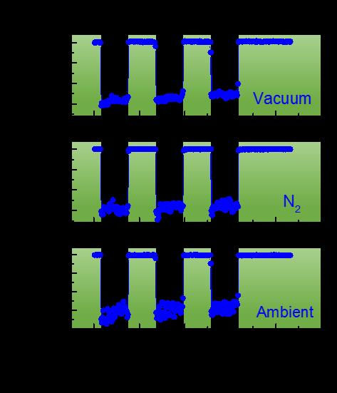
6 exhibits a much faster photoresponse and the PPC effect can be greatly suppressed when the photocurrent is dominated by the short-circuit current. Interestingly, the short-circuit photocurrent is virtually insensitive to the variation of the gaseous conditions over a range from a vacuum of Torr to ambient condition. Here, we present this unique characteristic by showing the V SD dependent photocurrent (I ph ) in different gaseous environment. Figure 2a compares I ph of a 1L-3L MoS2 junction (sample B) at V SD = 0 mv among vacuum, N2 (1 atm), and ambient condition, revealing that the magnitude of the I SC ( I SC ) is insensitive to the environment. We note that in all 5 1L-3L samples that we measured, the photoresponse behavior is comparable and therefore the data shown here is representative. Under very different pressure and chemical substances, I SC exhibits essentially the same value of approximately 140 pa. Moreover, the decay time (τ) values for these different conditions are also similar, as described in detail in supporting information S3. In contrast, the photocurrent of sample B under bias critically depends on the environmental conditions. Figure 2b shows I ph at V SD = 5 mv under vacuum, N2, and ambient conditions, indicating the changes in photocurrent ( I PC ) for these three conditions are 263, 133, and 41 pa, respectively. Here we note that while I SC is only governed by the built-in electric field, I PC is referred to PC that is determined by both built-in field and external bias. Moreover, the sample exhibits larger τ under vacuum (90 sec) as compared to the τ under N2 (16 sec) and ambient (8 sec) conditions. This dependence of I ph on the chemical environment is typical for the 2D-material devices. The extracted parameters of mobility, threshold voltage, I SC, and I PC are listed in Table 1. As previously discussed, I SC is driven by the diffusion current that is related to the gradient of carrier density. This gradient is associated with the condition of illumination, but is negligibly affected by the trapping process and the presence of adsorbents. Consequently, both the magnitude and the 6
7 response time of I SC are very insensitive to the gaseous environment, despite the pressure and the chemical composition being very different. We note that this insensitivity of the photocurrent in MoS2 junctions is very uncommon in 2D-material-based devices, considering the ultrahigh surface-tovolume ratio that leads to a large area being exposed to absorbents. Conversely, when bias voltage is applied, the carriers could be trapped or released during illumination and dark conditions, leading to the charging and the PPC effect, as seen in Figure 2b. Vacuum N 2 Ambient mobility 0.5 cm 2 Vs 0.14 cm 2 Vs 0.09 cm 2 Vs threshold voltage 5.5 V 20 V 25.5 V I SC V SD = 0 mv 136 pa 143 pa 149 pa I PC V SD = 5 mv 263 pa 133 pa 41 pa Table 1. The characteristics of the MoS2 junction (sample B) under different gaseous conditions. To further investigate the observed PV effect due to the built-in electric field, we present the V SD dependence of the photocurrent. Figure 3a shows a schematic diagram of energy band alignment and photoinduced carrier dynamics in the MoS2 heterojunction. Type-I band alignment is implied based on the STS results shown in Figures 4d and 4e. At zero bias, the photocurrent is mainly driven by the built-in field under illumination (Supporting Information S4), whereas both the built-in and the external field co-exist when bias voltage is applied. It is noted that only the electron conduction is considered here because all the MoS2 junction samples exhibit n-type semiconducting behavior (Supporting Information S1). We considered the photocurrent under two polarity of bias (the detailed calculation of I SC and I PC are described in Supporting Information S5). The fast photoresponse of the photocurrent is negative, regardless of the polarity of bias, indicating that I SC is induced by the built-in electric field. We then compared the photocurrent of sample B corresponding to the PV and the charging/discharging effect as a function of V SD in small bias regime, as shown Figure 3b. I SC is 7
8 found to be relatively independent of V SD ; this response is ascribed to the cancellation of the external field. In contrast, I PC, and thus the charging/discharging effect, increases linearly with V SD ; this response may be due to the phenomenon that the carriers are driven to the local potential minimum more efficiently with increasing bias. Figure 4a shows a schematic of the experimental setup for the STM measurement on the MoS2 junction transistors. Before MoS2 exfoliation, we deposited a thin TiOx film of 5 nm, 38 which served as electron transfer dopant on MoS2 flakes, 39 resulting in the reduction of MoS2 sheet resistance. The deposition of a TiOx layer is therefore crucial for preventing of the STM tip from crashing during the measurement. Figure 4b shows a topography image of the MoS2 junction device (sample C) at the junction, revealing the step with two flat terraces. The apparent step height is 2.6 nm, corresponding to 4 layers of MoS2. Because the thinner MoS2 is characterized by AFM as 4 layers, the studied MoS2 sample is therefore a 4- to 8-layer junction. Figure 4c shows a high magnification topography image of MoS2 that reveals crystalline structure, indicating a pristine MoS2 surface. To investigate the band alignment at the MoS2 junction, the STS technique was utilized to measure the normalized di/dv as a function of bias, which corresponds to the local density of state (LDOS). Figure 4d shows the bias dependence of di/dv curve for the two MoS2 terraces with different thicknesses. The onsets of the normalized di/dv curves at positive and negative bias correspond to the conduction band edge (E C ) and the valance band edge (E V ), respectively (Supporting information S6). From the STS measurement, we deduce the following: the E C and E V in 8-layer MoS2 are 0.29 ev and ev, respectively; the E C and E V in 4-layer MoS2 are 0.44 ev and ev, respectively. By spatially mapping the normalized di/dv curves, we plot the band alignment across the 4- to 8-layer junction, as shown in Figure 4e. The deduced energy profile suggests that the band alignment of the MoS2 junction is type I, as depicted in Figure 3a. 8
9 Finally, we present the current-voltage characteristics at different V G to analyze the field effect of the photocurrent in the MoS2 junction devices. Figure 5a compares the I SD V SD curves of sample B in dark and under illumination with a 532 nm laser and 20 kw/cm 2 at V G = 60 V. The I SD V SD curves exhibit a linear behavior, indicating that resistor behavior, rather than the rectifying effect, dominates the transport property of the junctions. The slope of the I SD V SD curves therefore approximates the conductance (G) of the device. Under illumination, G is enhanced by 40 times compared with G in dark; this enhancement is attributed to the generation of the photoinduced carriers. The open-circuit voltage (V OC ) and I SC can be extracted as 60 μv and 0.12 na, respectively. We note that the I SC can be further enhanced by reducing the Schottky barrier height via contact engineering. Because the Fermi level in thin materials can be effectively tuned by the external electric field, it is intriguing to study the field effect of the current-voltage characteristics. Indeed, we observed a V G dependence of the I SD V SD curves under illumination, as shown in Figure 5b, in which G increases with increasing V G. To understand this field effect, we plot V OC and I SC as a function of V G, as shown in Figure 5c. I SC is found to increase with increasing V G, similar to the I SD V G curve (see Figure S1 of SI 1). This similarity is reasonable because I SC depends on the collection probability of the photoinduced carriers, which is correlated to the diffusion current and G. Moreover, as V G increases, the contact resistance may decrease due to Schottky barrier thinning, 40 leading to higher I SC. Conversely, the response of V OC decreasing with increasing V G can be attributed to the reduction of built-in electric field in the MoS2 junction. Because monolayer MoS2 is subjected to a stronger field effect compared with the few-layer MoS2 due to the different density of states, the rising of Fermi level in monolayer MoS2 is greater than that in few-layer MoS2 as V G increases, resulting in the reduction of the built-in electric field (see Figure 3a) and thus V OC. 9
10 We further present the excitation power dependence of I SC at zero bias voltage (Figure 5d) to examine the mechanism of the photocurrent generation. 41 We observe that I SC follows a power law I SC P α, and the exponent α can be been extracted as 0.89 and 0.82 for V G = 0 and 60 V, respectively. For the PC and the PV process, the photoinduced carrier density is directly proportional to the rate of absorbed photons; therefore, α = However, because the PC is excluded here (V SD = 0), the value of α therefore suggests that the PV is the dominant mechanism in the measured photocurrent. The deviation of the extracted α from unity may be attributed to electron-hole recombination at the MoS2 junction and/or nonradiative recombination centers. 43,44 In conclusion, we demonstrated a unique environment-insensitive and gate-controllable shortcircuit photocurrent in a MoS2 junction with differences in the number of layer. The environmental insensitivity of the short-circuit photocurrent can be attributed to the characteristic of the diffusion current. Conversely, the photocurrent with bias exhibits the typical PPC that greatly depends on the amount of the extrinsic adsorbents. The STM/STS measurement confirms the quality of the MoS2 junction samples and suggests the type-i band alignment of the junction. In addition to the effect of source-drain bias, the MoS2 junction devices exhibit strong back-gate voltage dependence, indicating the feasibility to control the photocurrent via field effect. The environment-insensitive photocurrent therefore shows an alternative method to design the device structure for TMDC-based electronic and optoelectronic applications. Methods Sample preparation. The sample with the 1L-3L MoS2 junction was produced via mechanical exfoliation of MoS2 layers from the bulk MoS2 (SPI supplies) onto SiO2 (300 nm)/si substrates. Next, a resist-free technique with a shadow mask (TEM grids) was utilized to deposit electrical contacts. The advantage of the resist-free technique is the lack of resist residue on the MoS2 surface resulting 10
11 from the device fabrication process. We deposited Au (50 nm) as the electrical contacts using an electron-beam evaporator at a base pressure of Torr. All of our MoS2 junction devices were measured in a cryostat (Janis Research Company, ST-500) under vacuum condition of Torr. We performed DC electrical measurement using a Keithley 237 sourcemeter and applied the back-gate voltage using a Keithley 2400 sourcemeter. We employed solid-state CW laser (Nd:YAG, 532 nm) as the light source in the Raman spectroscopy and photoresponse measurements. The incident light beam was focused by an objective (100, NA 0.6) with a spot size of ~ 0.9 μm. References 1 Geim, A. K. & Novoselov, K. S. The rise of graphene. Nature materials 6, (2007). 2 Schedin, F. et al. Detection of individual gas molecules adsorbed on graphene. Nature materials 6, (2007). 3 Varghese, S. S., Varghese, S. H., Swaminathan, S., Singh, K. K. & Mittal, V. Two- Dimensional Materials for Sensing: Graphene and Beyond. Electronics 4, (2015). 4 Tongay, S. et al. Broad-range modulation of light emission in two-dimensional semiconductors by molecular physisorption gating. Nano letters 13, (2013). 5 He, R. et al. Large physisorption strain in chemical vapor deposition of graphene on copper substrates. Nano letters 12, (2012). 6 Perkins, F. K. et al. Chemical vapor sensing with monolayer MoS2. Nano letters 13, (2013). 7 Ando, T. Screening effect and impurity scattering in monolayer graphene. Journal of the Physical Society of Japan 75, (2006). 8 Hwang, E., Adam, S. & Sarma, S. D. Carrier transport in two-dimensional graphene layers. Physical Review Letters 98, (2007). 9 Bolotin, K. I. et al. Ultrahigh electron mobility in suspended graphene. Solid State Communications 146, (2008). 10 Ma, N. & Jena, D. Charge scattering and mobility in atomically thin semiconductors. Physical Review X 4, (2014). 11 Furchi, M. M., Polyushkin, D. K., Pospischil, A. & Mueller, T. Mechanisms of Photoconductivity in Atomically Thin MoS2. Nano Lett. 14, , doi: /n q (2014). 12 Chen, J.-H. et al. Charged-impurity scattering in graphene. Nature Physics 4, (2008). 13 Tan, Y.-W. et al. Measurement of scattering rate and minimum conductivity in graphene. Physical review letters 99, (2007). 14 Chen, J.-H., Jang, C., Xiao, S., Ishigami, M. & Fuhrer, M. S. Intrinsic and extrinsic performance limits of graphene devices on SiO2. Nature nanotechnology 3, (2008). 15 Jena, D. & Konar, A. Enhancement of carrier mobility in semiconductor nanostructures by dielectric engineering. Physical review letters 98, (2007). 16 Kretinin, A. et al. Electronic properties of graphene encapsulated with different twodimensional atomic crystals. Nano letters 14, (2014). 11
12 17 Ho, P.-H. et al. Self-encapsulated doping of n-type graphene transistors with extended air stability. ACS nano 6, (2012). 18 Lee, G.-H. et al. Highly Stable, Dual-Gated MoS2 Transistors Encapsulated by Hexagonal Boron Nitride with Gate-Controllable Contact, Resistance, and Threshold Voltage. ACS nano 9, (2015). 19 Li, L. et al. Quantum Hall effect in black phosphorus two-dimensional electron system. Nature Nanotechnology (2016). 20 Kuc, A., Zibouche, N. & Heine, T. Influence of quantum confinement on the electronic structure of the transition metal sulfide T S 2. Physical Review B 83, (2011). 21 Yun, W. S., Han, S., Hong, S. C., Kim, I. G. & Lee, J. Thickness and strain effects on electronic structures of transition metal dichalcogenides: 2H-M X 2 semiconductors (M= Mo, W; X= S, Se, Te). Physical Review B 85, (2012). 22 Mak, K. F., Lee, C., Hone, J., Shan, J. & Heinz, T. F. Atomically thin MoS 2: a new directgap semiconductor. Physical Review Letters 105, (2010). 23 Splendiani, A. et al. Emerging photoluminescence in monolayer MoS2. Nano letters 10, (2010). 24 Cheiwchanchamnangij, T. & Lambrecht, W. R. Quasiparticle band structure calculation of monolayer, bilayer, and bulk MoS 2. Physical Review B 85, (2012). 25 Howell, S. L. et al. Investigation of Band-Offsets at Monolayer Multilayer MoS2 Junctions by Scanning Photocurrent Microscopy. Nano letters 15, (2015). 26 Tosun, M. et al. MoS2 Heterojunctions by Thickness Modulation. Scientific reports 5 (2015). 27 Baugher, B. W. H., Churchill, H. O. H., Yang, Y. F. & Jarillo-Herrero, P. Optoelectronic devices based on electrically tunable p-n diodes in a monolayer dichalcogenide. Nat Nanotechnol 9, , doi: /nnano (2014). 28 Pospischil, A., Furchi, M. M. & Mueller, T. Solar-energy conversion and light emission in an atomic monolayer p-n diode. Nat Nanotechnol 9, , doi: /nnano (2014). 29 Fontana, M. et al. Electron-hole transport and photovoltaic effect in gated MoS2 Schottky junctions. Sci Rep-Uk 3, doi:artn 1634 Doi /Srep01634 (2013). 30 Wu, Y. C. et al. Extrinsic Origin of Persistent Photoconductivity in Monolayer MoS2 Field Effect Transistors. Sci Rep 5, 11472, doi: /srep11472 (2015). 31 Jiang, H. X. & Lin, J. Y. Percolation transition of persistent photoconductivity in II-VI mixed crystals. Phys Rev Lett 64, , doi:doi /PhysRevLett (1990). 32 Dissanayake, A. S., Huang, S. X., Jiang, H. X. & Lin, J. Y. Charge Storage and Persistent Photoconductivity in a Cds0.5se0.5 Semiconductor Alloy. Phys Rev B 44, , doi:doi /PhysRevB (1991). 33 Palmer, R. G., Stein, D. L., Abrahams, E. & Anderson, P. W. Models of Hierarchically Constrained Dynamics for Glassy Relaxation. Phys. Rev. Lett. 53, (1984). 34 Yin, Z. Y. et al. Single-Layer MoS2 Phototransistors. ACS Nano 6, 74-80, doi:doi /Nn (2012). 35 Lee, H. S. et al. MoS2 Nanosheet Phototransistors with Thickness-Modulated Optical Energy Gap. Nano Lett. 12, , doi:doi /Nl301485q (2012). 36 Chen, S. Y. et al. Biologically inspired graphene-chlorophyll phototransistors with high gain. Carbon 63, 23-29, doi: /j.carbon (2013). 37 Sze, S. M. & Ng, K. K. Physics of semiconductor devices. (John wiley & sons, 2006). 38 Ho, P. H. et al. Precisely Controlled Ultrastrong Photoinduced Doping at Graphene Heterostructures Assisted by Trap State Mediated Charge Transfer. Advanced materials 27, (2015). 12
13 39 Rai, A. et al. Air stable doping and intrinsic mobility enhancement in monolayer molybdenum disulfide by amorphous titanium suboxide encapsulation. Nano letters 15, (2015). 40 Li, S.-L. et al. Thickness Scaling Effect on Interfacial Barrier and Electrical Contact to Two- Dimensional MoS2 Layers. ACS Nano, doi: /nn506138y (2014). 41 Zhang, Y. et al. Photothermoelectric and photovoltaic effects both present in MoS2. Scientific reports 5, 7938, doi: /srep07938 (2015). 42 Patil, V., Capone, A., Strauf, S. & Yang, E.-H. Improved photoresponse with enhanced photoelectric contribution in fully suspended graphene photodetectors. Scientific reports 3 (2013). 43 Zhang, W. et al. High-gain phototransistors based on a CVD MoS(2) monolayer. Advanced materials 25, , doi: /adma (2013). 44 Cho, K. et al. Gate-bias stress-dependent photoconductive characteristics of multi-layer MoS2 field-effect transistors. Nanotechnology 25, , doi: / /25/15/ (2014). 13
14 ACKNOWLEDGMENT This work was supported by the Ministry of Science and Technology, Taiwan under contract numbers MOST M MY3. Author Contributions Statement W.H.W. supervised the project. W.H.W., F.Y.S., and Y.C.W. designed the experiments. Y.S.S., M.C.S., and Y.P.C. performed the STM and STS measurement and analysis. P.H.H. and C.W.C. provided the OTS-functionalized substrates. F.Y.S., Y.C.W., and T.S.W. prepared the samples and carried out the photoresponse and transport measurements. F.Y.S., Y.C.W., and T.S.W. analyzed the data. W.H.W, F.Y.S., C.W.C., Y.F.C. and Y.P.C. wrote the paper. All authors discussed the results and contributed to the refinement of the paper. Additional information Competing financial interests: The authors declare no competing financial interests. 14
15 Figure Legends Figure 1. The structure and the photoresponse behaviors of the MoS2 junctions. (a) A schematic diagram of a 1L-3L MoS2 junction transistor with the excitation beam focused on the MoS2 junction. (b) Optical image of a MoS2 junction transistor. The edge of the MoS2 junction is outlined by red lines. (c) Time-resolved photoresponse behaviors of the MoS2 junction transistor (sample A) under V SD = 50 mv (red curve) and V SD = 0 mv (blue curve) at V G = 60 V. Figure 2. Time-resolved photoresponse of the MoS2 junctions. The photocurrent behavior of the MoS2 junction transistor (sample B) under different gaseous conditions at (a) V SD = 0 mv and (b) V SD = 5 mv. The short-circuit photoresponse is virtually insensitive to the variation of the gaseous conditions. Figure 3. VSD-dependent photoresponse of the MoS2 junctions. (a) A schematic of the band structure of the MoS2 junction transistor and photoinduced carrier transfer at V SD = 0 V and V SD 0 V. (b) The photocurrent measurement of sample B corresponding to the photovoltaic effect (black squares) and the photoconductivity effect (red squares) as a function of V SD at V G = 60 V. The excitation power is 200 μw. Figure 4. The STM/STS measurement of the MoS2 junctions. (a) A schematic of the MoS2 junction structure with different layer in the STM/STS measurement. (b) Top: STM topography image of the MoS2 junction (sample C). Bottom: a cross-sectional topographic profile of the MoS2 junction. (c) An STM image of sample C with atomic-scale resolution, which indicates a pristine MoS2 surface. (d) Normalized di/dv curves of 4 layer (green curve) and 8 layer (red curve) MoS2. The profiles are 15
16 offset for clarity. (e) Band alignment across the MoS2 4- to 8-layer junction. Type-I band alignment at the MoS2 junction was implied. Figure 5. Field-effect-controlled short-circuit photocurrent of the MoS2 junction transistors. (a) Output curves of the MoS2 junction device (sample B) in dark (black curve) and under 532 nm excitation focused on the MoS2 junction (red curve) at V G = 60 V. (b) V G dependence of the output curves under laser illumination (P = 200 μw) at the MoS2 junction. (c) Analysis of V G dependence of V OC and I SC extracted from the output curves. (d) Excitation power dependence of I SC at zero bias at V G = 0 V (black squares) and V G = 60 V (red circles). The dashed lines are fitting curves of power law I SC P α. 16
")


17 (a) (b) (c)

18 (a) (b)


19 (a) (b) I ph (na) I SC I PC V SD (mv)


20
21 (a) I SD (na) (c) V SD (mv) dark illumination 150 (b) I SD (na) (d) V SD (mv) V G 0V 10V 20V 30V 40V 50V 60V V OC ( V) V G (V) I SC (pa) I SC (na) I SC P 0.82 V G = 60 V I SC P 0.89 V G = 0 V V SD = 0 mv Power ( W)
22 Supporting Information Environment-insensitive and gate-controllable photocurrent enabled by bandgap engineering of MoS2 junctions Fu-Yu Shih 1,2, Yueh-Chun Wu 2,, Yi-Siang Shih 1, Ming-Chiuan Shih 3, Tsuei-Shin Wu 1,2, Po-Hsun Ho 4, Chun-Wei Chen 4, Yang-Fang Chen 1, Ya-Ping Chiu 1,5, and Wei-Hua Wang 2* 1 Department of Physics, National Taiwan University, Taipei 106, Taiwan 2 Institute of Atomic and Molecular Sciences, Academia Sinica, Taipei 106, Taiwan 3 Department of Physics, National Sun Yat-sen University, Kaohsiung, Taiwan 4 Department of Materials Science and Engineering, National Taiwan University, Taipei 106, Taiwan 5 Institute of Physics, Academia Sinica, Taipei 115, Taiwan Current address: Department of Physics, University of Massachusetts, Amherst, Massachusetts 01003, United States * Corresponding Author. (W.-H. Wang) Tel: , Fax: ; wwang@sinica.edu.tw
23 S1. Device fabrication and photocurrent measurement The sample with the 1L-3L MoS2 junction was produced via mechanical exfoliation of MoS2 layers from the bulk MoS2 (SPI supplies) onto SiO2 (300 nm)/si substrates. Next, a resist-free technique with a shadow mask (TEM grids) was utilized to deposit electrical contacts. The advantage of the resist-free technique is the lack of resist residue on the MoS2 surface resulting from the device fabrication process. We deposited Au (50 nm) as the electrical contacts using an electron-beam evaporator at a base pressure of Torr. All of our MoS2 junction devices were measured in a cryostat (Janis Research Company, ST-500) under vacuum condition of Torr. We performed DC electrical measurement using a Keithley 237 sourcemeter and applied the back-gate voltage using a Keithley 2400 sourcemeter. We employed solid-state CW laser (Nd:YAG, 532 nm) as the light source in the Raman spectroscopy and photoresponse measurements. The incident light beam was focused by an objective (100, NA 0.6) with a spot size of ~ 0.9 μm. Figure S1 compares the I SD V G curves of a 1L-3L MoS2 junction device (sample B of the main text) under vacuum, N2, and ambient conditions. The MoS2 junction device exhibits typical n-type semiconducting behavior. The sample exhibits higher mobility under vacuum (0.5 cm 2 /Vs) compared to the mobility under N2 (0.14 cm 2 /Vs) and ambient (0.09 cm 2 /Vs) conditions. This difference can be understood because the carrier scattering is higher when additional adsorbents are introduced in the environment with abundant molecules [1]. The on/off ratio is approximately The threshold for N2 and ambient conditions is higher than that under vacuum, suggesting a p-type doping effect is introduced during the adsorption [2, 3].


24 Figure S1. The transfer curves of 1L-3L MoS2 junction device under vacuum, N2, and ambient conditions.
25 S2 Identification of the number of MoS2 layers The layer number of the MoS2 flakes was identified using optical microscopy, Raman spectroscopy, and atomic force microscopy (AFM) measurements. Figure S2a presents an optical image of MoS2 flake on 300-nm SiO2/Si substrate involving monolayer and trilayer MoS2 (sample A of the main text). The Raman spectra (Figure S2b) reveals two characteristic peaks (386.6) cm - 1 and 407 (409.1) cm -1 1 of the monolayer (trilayer) MoS2 flake, which correspond to the E 2g and A 1g resonance modes, respectively. The difference between the two peaks can be used to identify the thickness of the MoS2, particularly for a number of layers less than 3 [4]. For this MoS2 junction sample, the difference is equal to 18.9 cm -1 for monolayer MoS2 and 22.5 cm -1 for trilayer MoS2, in agreement with previous reports [4]. We performed AFM measurement in a region denoted by a red rectangle shown in Figure S2a. The result is presented in Figure S2c, which shows that the step height of the thinner area of the MoS2 junction was approximately 0.7 nm, which corresponds to one atomic layer. The step height of the thicker area of the MoS2 junction was approximately 1.9 nm, which corresponds to trilayer MoS2.
 Optical microscope image")
 AFM image of 1L-3L MoS2")
26 Figure S2. (a) Optical microscope image and (b) Raman spectra and (c) AFM image of 1L-3L MoS2 junction (Sample A).

 = I 0 exp (t τ). The values of τ under ambient, N2, and vacuum condition were extracted as 61.8 ms, 63.8 ms, and 62.1 ms, respectively.")
27 S3 Estimation of the decay time under different gaseous conditions We measured the time-resolved photocurrent by using the built-in sweep function of the Keithley 237 sourcemeter with the setting-reading cycle of 18 ms. Figure S3a shows the time-resolved photocurrent (black squares) at zero bias voltage under ambient, N2, and vacuum condition, respectively along with the fitting curves (red lines) based on normal exponential decay, I(t) = I 0 exp (t τ). The values of τ under ambient, N2, and vacuum condition were extracted as 61.8 ms, 63.8 ms, and 62.1 ms, respectively. The value of τ is found to be approximately the same under different environmental conditions. Figure S3b shows time-resolved photocurrent at V SD = 5 mv under ambient, N2 and vacuum conditions along with the fitting curves (green lines) based on stretched exponential decay, I(t) = I 0 exp[ (t τ) β ]. The extracted τ is found to be dependent on the environment; this result can be attributed to the random localized potential fluctuations in MoS2 [5]. Figure S3. Time-resolved photocurrent measurement at (a) zero bias and (b) V SD = 5 mv under different gaseous conditions. The red and green curves represent the fitting curves based on normal exponential decay and stretched exponential decay, respectively.

 under different")
28 Table S1. The decay time of the MoS2 junction (sample B) under different gaseous conditions.
.")
29 S4 Zero-bias time-resolved photoresponse in a uniform MoS2 transistor The observed zero-bias photocurrent in the MoS2 junction device is due to the band offset resulting from the different thicknesses of MoS2. To verify this characteristic, we present the zero-bias photocurrent measurement in a uniform MoS2 device, which shows no photoresponse when illuminated at zero bias (Figure S4). This lack of photoresponse is in contrast to the observed photoresponse measured in the MoS2 junction device, as shown in Figures 1c and 2a in the main text. Figure S4. Time-resolved photoresponse of uniform 1L MoS2 at zero-bias voltage.
30 S5 Analysis of V SD dependence of the photocurrent due to the PV and the PC effect Figures S5a and S5b show the temporal photoresponse of the 1L-3L MoS2 junction device under small bias (V SD = ±2 mv). The direction of the photocurrent with slow response is found to depend on the direction of the external electric field. In contrast, the direction of the photocurrent with quick response is observed to retain a specific direction, suggesting that the photocurrent with quick response is mainly caused by the junction-induced built-in electric field. To distinguish the photocurrent corresponding to the PV effect versus the PC effect, we define I SC and I PC as: I SC = (I VSD =x mv + I VSD = x mv) 2 Eqn. S1 I PC = ( I PC,VSD =x mv + I PC,VSD = x mv ) 2 Eqn. S2 where I VSD =x mv is the change of photocurrent with quick response at V SD = x mv, and I PC,VSD =x mv is the change of photocurrent with slow response at V SD = x mv. The photocurrent caused by external bias with quick response is cancelled by summing up the contributions from the two polarities of the bias voltages. Therefore, I SC represents the photocurrent resulting from the builtin electric field. Alternatively, we take the average of the absolute value of the photocurrent with slow response under the two polarities of bias to represent the photocurrent due to the PC effect.

31 Figure S5. Time-resolved photocurrent of 1L-3L MoS2 junction under small bias (V SD = ±2 mv).
32 S6 STM/STS characterization In STS measurements, the STM probe tip, vacuum and MoS2 form a metal-insulatorsemiconductor (MIS) tunneling junction. When we apply zero sample bias on the sample so that there is no tunneling current between tip and MoS2, the Fermi-level of the tip is equal to the Fermi-level of the MoS2 under thermal equilibrium. Therefore, the zero sample bias can be defined as the Fermi-level of the sample. In contrast to the zero sample bias condition, when we apply a certain sample bias on the sample, the tunneling current flows between the probe tip and MoS2. As a result, the onsets in the normalized di/dv curves indicate the current onsets from the valance band edge (E V ) and the conduction band edge (E C ) in STM measurements.
33 References 1. Qiu, H., et al., Electrical characterization of back-gated bi-layer MoS2 field-effect transistors and the effect of ambient on their performances. Applied Physics Letters, (12): p Tongay, S., et al., Broad-range modulation of light emission in two-dimensional semiconductors by molecular physisorption gating. Nano letters, (6): p Yue, Q., et al., Adsorption of gas molecules on monolayer MoS2 and effect of applied electric field. Nanoscale research letters, (1): p Li, H., et al., From bulk to monolayer MoS2: evolution of Raman scattering. Advanced Functional Materials, (7): p Wu, Y.-C., et al., Extrinsic Origin of Persistent Photoconductivity in Monolayer MoS2 Field Effect Transistors. arxiv preprint arxiv: , 2015.
Extrinsic Origin of Persistent Photoconductivity in
 Supporting Information Extrinsic Origin of Persistent Photoconductivity in Monolayer MoS2 Field Effect Transistors Yueh-Chun Wu 1, Cheng-Hua Liu 1,2, Shao-Yu Chen 1, Fu-Yu Shih 1,2, Po-Hsun Ho 3, Chun-Wei
Supplementary Figure 1. Supplementary Figure 1 Characterization of another locally gated PN junction based on boron
 Supplementary Figure 1 Supplementary Figure 1 Characterization of another locally gated PN junction based on boron nitride and few-layer black phosphorus (device S1). (a) Optical micrograph of device S1.
Extrinsic Origin of Persistent Photoconductivity in Monolayer MoS 2 Field Effect Transistors
 Extrinsic Origin of Persistent Photoconductivity in Monolayer MoS 2 Field Effect Transistors Yueh-Chun Wu 1, Cheng-Hua Liu 1,2, Shao-Yu Chen 1, Fu-Yu Shih 1,2, Po-Hsun Ho 3, Chun-Wei Chen 3, Chi-Te Liang
Supporting Information Available:
 Supporting Information Available: Photoresponsive and Gas Sensing Field-Effect Transistors based on Multilayer WS 2 Nanoflakes Nengjie Huo 1, Shengxue Yang 1, Zhongming Wei 2, Shu-Shen Li 1, Jian-Bai Xia
Supporting Information
 Supporting Information Spatially-resolved imaging on photocarrier generations and band alignments at perovskite/pbi2 hetero-interfaces of perovskite solar cells by light-modulated scanning tunneling microscopy
Graphene photodetectors with ultra-broadband and high responsivity at room temperature
 SUPPLEMENTARY INFORMATION DOI: 10.1038/NNANO.2014.31 Graphene photodetectors with ultra-broadband and high responsivity at room temperature Chang-Hua Liu 1, You-Chia Chang 2, Ted Norris 1.2* and Zhaohui
Supplementary Figure 1. Selected area electron diffraction (SAED) of bilayer graphene and tblg. (a) AB
 of bilayer graphene and tblg. (a) AB") Supplementary Figure 1. Selected area electron diffraction (SAED) of bilayer graphene and tblg. (a) AB stacked bilayer graphene (b), (c), (d), (e), and (f) are twisted bilayer graphene with twist angle
Supplementary Figure 1. Selected area electron diffraction (SAED) of bilayer graphene and tblg. (a) AB stacked bilayer graphene (b), (c), (d), (e), and (f) are twisted bilayer graphene with twist angle
Supplementary Figure 2 Photoluminescence in 1L- (black line) and 7L-MoS 2 (red line) of the Figure 1B with illuminated wavelength of 543 nm.
 and 7L-MoS 2 (red line) of the Figure 1B with illuminated wavelength of 543 nm.") PL (normalized) Intensity (arb. u.) 1 1 8 7L-MoS 1L-MoS 6 4 37 38 39 4 41 4 Raman shift (cm -1 ) Supplementary Figure 1 Raman spectra of the Figure 1B at the 1L-MoS area (black line) and 7L-MoS area (red
PL (normalized) Intensity (arb. u.) 1 1 8 7L-MoS 1L-MoS 6 4 37 38 39 4 41 4 Raman shift (cm -1 ) Supplementary Figure 1 Raman spectra of the Figure 1B at the 1L-MoS area (black line) and 7L-MoS area (red
SUPPLEMENTARY INFORMATION
 Supplementary Information: Photocurrent generation in semiconducting and metallic carbon nanotubes Maria Barkelid 1*, Val Zwiller 1 1 Kavli Institute of Nanoscience, Delft University of Technology, Delft,
Supporting Information. by Hexagonal Boron Nitride
 Supporting Information High Velocity Saturation in Graphene Encapsulated by Hexagonal Boron Nitride Megan A. Yamoah 1,2,, Wenmin Yang 1,3, Eric Pop 4,5,6, David Goldhaber-Gordon 1 * 1 Department of Physics,
(a) (b) Supplementary Figure 1. (a) (b) (a) Supplementary Figure 2. (a) (b) (c) (d) (e)
 (b) Supplementary Figure 1. (a) (b) (a) Supplementary Figure 2. (a) (b) (c) (d) (e)") (a) (b) Supplementary Figure 1. (a) An AFM image of the device after the formation of the contact electrodes and the top gate dielectric Al 2 O 3. (b) A line scan performed along the white dashed line
(a) (b) Supplementary Figure 1. (a) An AFM image of the device after the formation of the contact electrodes and the top gate dielectric Al 2 O 3. (b) A line scan performed along the white dashed line
Ultrafast Lateral Photo-Dember Effect in Graphene. Induced by Nonequilibrium Hot Carrier Dynamics
 1 Ultrafast Lateral Photo-Dember Effect in Graphene Induced by Nonequilibrium Hot Carrier Dynamics Chang-Hua Liu, You-Chia Chang, Seunghyun Lee, Yaozhong Zhang, Yafei Zhang, Theodore B. Norris,*,, and
vapour deposition. Raman peaks of the monolayer sample grown by chemical vapour
 Supplementary Figure 1 Raman spectrum of monolayer MoS 2 grown by chemical vapour deposition. Raman peaks of the monolayer sample grown by chemical vapour deposition (S-CVD) are peak which is at 385 cm
SUPPLEMENTARY INFORMATION
 Hihly efficient ate-tunable photocurrent eneration in vertical heterostructures of layered materials Woo Jon Yu, Yuan Liu, Hailon Zhou, Anxian Yin, Zhen Li, Yu Huan, and Xianfen Duan. Schematic illustration
Fermi Level Pinning at Electrical Metal Contacts. of Monolayer Molybdenum Dichalcogenides
 Supporting information Fermi Level Pinning at Electrical Metal Contacts of Monolayer Molybdenum Dichalcogenides Changsik Kim 1,, Inyong Moon 1,, Daeyeong Lee 1, Min Sup Choi 1, Faisal Ahmed 1,2, Seunggeol
Supplementary Figure S1. AFM images of GraNRs grown with standard growth process. Each of these pictures show GraNRs prepared independently,
 Supplementary Figure S1. AFM images of GraNRs grown with standard growth process. Each of these pictures show GraNRs prepared independently, suggesting that the results is reproducible. Supplementary Figure
Black phosphorus: A new bandgap tuning knob
 Black phosphorus: A new bandgap tuning knob Rafael Roldán and Andres Castellanos-Gomez Modern electronics rely on devices whose functionality can be adjusted by the end-user with an external knob. A new
Supplementary material for High responsivity mid-infrared graphene detectors with antenna-enhanced photo-carrier generation and collection
 Supplementary material for High responsivity mid-infrared graphene detectors with antenna-enhanced photo-carrier generation and collection Yu Yao 1, Raji Shankar 1, Patrick Rauter 1, Yi Song 2, Jing Kong
Spatially resolving density-dependent screening around a single charged atom in graphene
 Supplementary Information for Spatially resolving density-dependent screening around a single charged atom in graphene Dillon Wong, Fabiano Corsetti, Yang Wang, Victor W. Brar, Hsin-Zon Tsai, Qiong Wu,
Graphene Canada Montreal Oct. 16, 2015 (International Year of Light)
") Luminescence Properties of Graphene A. Beltaos 1,2,3, A. Bergren 1, K. Bosnick 1, N. Pekas 1, A. Matković 4, A. Meldrum 2 1 National Institute for Nanotechnology (NINT), 11421 Saskatchewan Drive, Edmonton,
Luminescence Properties of Graphene A. Beltaos 1,2,3, A. Bergren 1, K. Bosnick 1, N. Pekas 1, A. Matković 4, A. Meldrum 2 1 National Institute for Nanotechnology (NINT), 11421 Saskatchewan Drive, Edmonton,
Monolayer Semiconductors
 Monolayer Semiconductors Gilbert Arias California State University San Bernardino University of Washington INT REU, 2013 Advisor: Xiaodong Xu (Dated: August 24, 2013) Abstract Silicon may be unable to
Supplementary Information for
 Supplementary Information for Highly Stable, Dual-Gated MoS 2 Transistors Encapsulated by Hexagonal Boron Nitride with Gate-Controllable Contact Resistance and Threshold Voltage Gwan-Hyoung Lee, Xu Cui,
UvA-DARE (Digital Academic Repository) Charge carrier dynamics in photovoltaic materials Jensen, S.A. Link to publication
 Charge carrier dynamics in photovoltaic materials Jensen, S.A. Link to publication") UvA-DARE (Digital Academic Repository) Charge carrier dynamics in photovoltaic materials Jensen, S.A. Link to publication Citation for published version (APA): Jensen, S. A. (2014). Charge carrier dynamics
UvA-DARE (Digital Academic Repository) Charge carrier dynamics in photovoltaic materials Jensen, S.A. Link to publication Citation for published version (APA): Jensen, S. A. (2014). Charge carrier dynamics
Title: Ultrafast photocurrent measurement of the escape time of electrons and holes from
 Title: Ultrafast photocurrent measurement of the escape time of electrons and holes from carbon nanotube PN junction photodiodes Authors: Nathaniel. M. Gabor 1,*, Zhaohui Zhong 2, Ken Bosnick 3, Paul L.
Supporting Information
 Supporting Information Monolithically Integrated Flexible Black Phosphorus Complementary Inverter Circuits Yuanda Liu, and Kah-Wee Ang* Department of Electrical and Computer Engineering National University
Intrinsic Electronic Transport Properties of High. Information
 Intrinsic Electronic Transport Properties of High Quality and MoS 2 : Supporting Information Britton W. H. Baugher, Hugh O. H. Churchill, Yafang Yang, and Pablo Jarillo-Herrero Department of Physics, Massachusetts
Rectification in a Black Phosphorus/WS2 van der. Waals Heterojunction Diode
 Supporting Information Temperature-Dependent and Gate-Tunable Rectification in a Black Phosphorus/WS2 van der Waals Heterojunction Diode Ghulam Dastgeer 1, Muhammad Farooq Khan 1, Ghazanfar Nazir 1, Amir
Supplementary Figure 1 Experimental setup for crystal growth. Schematic drawing of the experimental setup for C 8 -BTBT crystal growth.
 Supplementary Figure 1 Experimental setup for crystal growth. Schematic drawing of the experimental setup for C 8 -BTBT crystal growth. Supplementary Figure 2 AFM study of the C 8 -BTBT crystal growth
Theoretical Study on Graphene Silicon Heterojunction Solar Cell
 Copyright 2015 American Scientific Publishers All rights reserved Printed in the United States of America Journal of Nanoelectronics and Optoelectronics Vol. 10, 1 5, 2015 Theoretical Study on Graphene
Supplementary Figure 1: MoS2 crystals on WSe2-EG and EG and WSe2 crystals on MoSe2-EG and EG.
 Supplementary Figure 1: MoS2 crystals on WSe2-EG and EG and WSe2 crystals on MoSe2-EG and EG. (a) The MoS2 crystals cover both of EG and WSe2/EG after the CVD growth (Scar bar: 400 nm) (b) shows TEM profiles
Supplementary Figure 1 XRD pattern of a defective TiO 2 thin film deposited on an FTO/glass substrate, along with an XRD pattern of bare FTO/glass
 Supplementary Figure 1 XRD pattern of a defective TiO 2 thin film deposited on an FTO/glass substrate, along with an XRD pattern of bare FTO/glass and a reference pattern of anatase TiO 2 (JSPDS No.: 21-1272).
Supporting Information
 Copyright WILEY-VCH Verlag GmbH & Co. KGaA, 69469 Weinheim, Germany, 2015. Supporting Information for Adv. Funct. Mater., DOI: 10.1002/adfm.201503131 Tuning the Excitonic States in MoS 2 /Graphene van
2D Materials for Gas Sensing
 2D Materials for Gas Sensing S. Guo, A. Rani, and M.E. Zaghloul Department of Electrical and Computer Engineering The George Washington University, Washington DC 20052 Outline Background Structures of
Tunneling characteristics of graphene
 Tunneling characteristics of graphene Young Jun Shin, 1,2 Gopinadhan Kalon, 1,2 Jaesung Son, 1 Jae Hyun Kwon, 1,2 Jing Niu, 1 Charanjit S. Bhatia, 1 Gengchiau Liang, 1 and Hyunsoo Yang 1,2,a) 1 Department
Strong light matter coupling in two-dimensional atomic crystals
 SUPPLEMENTARY INFORMATION DOI: 10.1038/NPHOTON.2014.304 Strong light matter coupling in two-dimensional atomic crystals Xiaoze Liu 1, 2, Tal Galfsky 1, 2, Zheng Sun 1, 2, Fengnian Xia 3, Erh-chen Lin 4,
1. Theoretical predictions for charged impurity scattering in graphene
 Supplementary Information 1. Theoretical predictions for charged impurity scattering in graphene We briefly review the state of theoretical and experimental work on zeromagnetic-field charge transport
SUPPLEMENTARY INFORMATION
 DOI: 1.138/NNANO.211.214 Control over topological insulator photocurrents with light polarization J.W. McIver*, D. Hsieh*, H. Steinberg, P. Jarillo-Herrero and N. Gedik SI I. Materials and device fabrication
Raman spectroscopy at the edges of multilayer graphene
 Raman spectroscopy at the edges of multilayer graphene Q. -Q. Li, X. Zhang, W. -P. Han, Y. Lu, W. Shi, J. -B. Wu, P. -H. Tan* State Key Laboratory of Superlattices and Microstructures, Institute of Semiconductors,
Supplementary Figure 1 Interlayer exciton PL peak position and heterostructure twisting angle. a, Photoluminescence from the interlayer exciton for
 Supplementary Figure 1 Interlayer exciton PL peak position and heterostructure twisting angle. a, Photoluminescence from the interlayer exciton for six WSe 2 -MoSe 2 heterostructures under cw laser excitation
SUPPLEMENTARY INFORMATION
 doi:10.1038/nature13734 1. Gate dependence of the negatively charged trion in WS 2 monolayer. We test the trion with both transport and optical measurements. The trion in our system is negatively charged,
The deposition of these three layers was achieved without breaking the vacuum. 30 nm Ni
 Transfer-free Growth of Atomically Thin Transition Metal Disulfides using a Solution Precursor by a Laser Irradiation Process and their Application in Low-power Photodetectors Chi-Chih Huang 1, Henry Medina
Supporting Online Material for
 www.sciencemag.org/cgi/content/full/science.1211384/dc1 Supporting Online Material for Hot Carrier Assisted Intrinsic Photoresponse in Graphene Nathaniel M. Gabor, Justin C. W. Song, Qiong Ma, Nityan L.
A. Optimizing the growth conditions of large-scale graphene films
 1 A. Optimizing the growth conditions of large-scale graphene films Figure S1. Optical microscope images of graphene films transferred on 300 nm SiO 2 /Si substrates. a, Images of the graphene films grown
Generation of photovoltage in graphene on a femtosecond timescale through efficient carrier heating
 DOI: 1.138/NNANO.215.54 Generation of photovoltage in graphene on a femtosecond timescale through efficient carrier heating K. J. Tielrooij, L. Piatkowski, M. Massicotte, A. Woessner, Q. Ma, Y. Lee, K.
Semiconductor Physical Electronics
 Semiconductor Physical Electronics Sheng S. Li Department of Electrical Engineering University of Florida Gainesville, Florida Plenum Press New York and London Contents CHAPTER 1. Classification of Solids
Sheng S. Li. Semiconductor Physical Electronics. Second Edition. With 230 Figures. 4) Springer
 Springer") Sheng S. Li Semiconductor Physical Electronics Second Edition With 230 Figures 4) Springer Contents Preface 1. Classification of Solids and Crystal Structure 1 1.1 Introduction 1 1.2 The Bravais Lattice
Sheng S. Li Semiconductor Physical Electronics Second Edition With 230 Figures 4) Springer Contents Preface 1. Classification of Solids and Crystal Structure 1 1.1 Introduction 1 1.2 The Bravais Lattice
Opto-electronic Characterization of Perovskite Thin Films & Solar Cells
 Opto-electronic Characterization of Perovskite Thin Films & Solar Cells Arman Mahboubi Soufiani Supervisors: Prof. Martin Green Prof. Gavin Conibeer Dr. Anita Ho-Baillie Dr. Murad Tayebjee 22 nd June 2017
SUPPLEMENTARY INFORMATION
 Dirac electron states formed at the heterointerface between a topological insulator and a conventional semiconductor 1. Surface morphology of InP substrate and the device Figure S1(a) shows a 10-μm-square
Multicolor Graphene Nanoribbon/Semiconductor Nanowire. Heterojunction Light-Emitting Diodes
 Multicolor Graphene Nanoribbon/Semiconductor Nanowire Heterojunction Light-Emitting Diodes Yu Ye, a Lin Gan, b Lun Dai, *a Hu Meng, a Feng Wei, a Yu Dai, a Zujin Shi, b Bin Yu, a Xuefeng Guo, b and Guogang
2. The electrochemical potential and Schottky barrier height should be quantified in the schematic of Figure 1.
 Reviewers' comments: Reviewer #1 (Remarks to the Author): The paper reports a photon enhanced thermionic effect (termed the photo thermionic effect) in graphene WSe2 graphene heterostructures. The work
Impact of Calcium on Transport Property of Graphene. Jyoti Katoch and Masa Ishigami*
 Impact of Calcium on Transport Property of Graphene Jyoti Katoch and Masa Ishigami* Department of Physics and Nanoscience Technology Center, University of Central Florida, Orlando, FL, 32816 *Corresponding
Center for Integrated Nanostructure Physics (CINAP)
") Center for Integrated Nanostructure Physics (CINAP) - Institute for Basic Science (IBS) was launched in 2012 by the Korean government to promote basic science in Korea - Our Center was established in 2012
Center for Integrated Nanostructure Physics (CINAP) - Institute for Basic Science (IBS) was launched in 2012 by the Korean government to promote basic science in Korea - Our Center was established in 2012
Supporting information. Gate-optimized thermoelectric power factor in ultrathin WSe2 single crystals
 Supporting information Gate-optimized thermoelectric power factor in ultrathin WSe2 single crystals Masaro Yoshida 1, Takahiko Iizuka 1, Yu Saito 1, Masaru Onga 1, Ryuji Suzuki 1, Yijin Zhang 1, Yoshihiro
Lecture 15: Optoelectronic devices: Introduction
 Lecture 15: Optoelectronic devices: Introduction Contents 1 Optical absorption 1 1.1 Absorption coefficient....................... 2 2 Optical recombination 5 3 Recombination and carrier lifetime 6 3.1
2) Atom manipulation. Xe / Ni(110) Model: Experiment:
 Atom manipulation. Xe / Ni(110) Model: Experiment:") 2) Atom manipulation D. Eigler & E. Schweizer, Nature 344, 524 (1990) Xe / Ni(110) Model: Experiment: G.Meyer, et al. Applied Physics A 68, 125 (1999) First the tip is approached close to the adsorbate
2) Atom manipulation D. Eigler & E. Schweizer, Nature 344, 524 (1990) Xe / Ni(110) Model: Experiment: G.Meyer, et al. Applied Physics A 68, 125 (1999) First the tip is approached close to the adsorbate
Ultrafast hot-carrier-dominated photocurrent in graphene
 SUPPLEMENTARY INFORMATION DOI: 10.1038/NNANO.2011.243 Ultrafast hot-carrier-dominated photocurrent in graphene Table of Contents: Dong Sun 1, Grant Aivazian 1, Aaron M. Jones 1, Jason S. Ross 2,Wang Yao
Electronic Supplementary Information for
 Electronic Supplementary Material (ESI) for Journal of Materials Chemistry C. This journal is The Royal Society of Chemistry 018 Electronic Supplementary Information for Broadband Photoresponse Based on
1. Nanotechnology & nanomaterials -- Functional nanomaterials enabled by nanotechnologies.
 Novel Nano-Engineered Semiconductors for Possible Photon Sources and Detectors NAI-CHANG YEH Department of Physics, California Institute of Technology 1. Nanotechnology & nanomaterials -- Functional nanomaterials
2D MBE Activities in Sheffield. I. Farrer, J. Heffernan Electronic and Electrical Engineering The University of Sheffield
 2D MBE Activities in Sheffield I. Farrer, J. Heffernan Electronic and Electrical Engineering The University of Sheffield Outline Motivation Van der Waals crystals The Transition Metal Di-Chalcogenides
Classification of Solids
 Classification of Solids Classification by conductivity, which is related to the band structure: (Filled bands are shown dark; D(E) = Density of states) Class Electron Density Density of States D(E) Examples
Metal Semiconductor Contacts
 Metal Semiconductor Contacts The investigation of rectification in metal-semiconductor contacts was first described by Braun [33-35], who discovered in 1874 the asymmetric nature of electrical conduction
SUPPLEMENTARY INFORMATION
 doi:.38/nature09979 I. Graphene material growth and transistor fabrication Top-gated graphene RF transistors were fabricated based on chemical vapor deposition (CVD) grown graphene on copper (Cu). Cu foil
Solar Cell Materials and Device Characterization
 Solar Cell Materials and Device Characterization April 3, 2012 The University of Toledo, Department of Physics and Astronomy SSARE, PVIC Principles and Varieties of Solar Energy (PHYS 4400) and Fundamentals
Supplementary Information
 Electronic Supplementary Material (ESI) for Physical Chemistry Chemical Physics. This journal is the Owner Societies 2015 Supplementary Information Vertical Heterostructures of MoS2 and Graphene Nanoribbons
(Co-PIs-Mark Brongersma, Yi Cui, Shanhui Fan) Stanford University. GCEP Research Symposium 2013 Stanford, CA October 9, 2013
 Stanford University. GCEP Research Symposium 2013 Stanford, CA October 9, 2013") High-efficiency thin film nano-structured multi-junction solar James S. cells Harris (PI) (Co-PIs-Mark Brongersma, Yi Cui, Shanhui Fan) Stanford University GCEP Research Symposium 2013 Stanford, CA October
High-efficiency thin film nano-structured multi-junction solar James S. cells Harris (PI) (Co-PIs-Mark Brongersma, Yi Cui, Shanhui Fan) Stanford University GCEP Research Symposium 2013 Stanford, CA October
Iodine-Mediated Chemical Vapor Deposition Growth of Metastable Transition Metal
 Supporting Information Iodine-Mediated Chemical Vapor Deposition Growth of Metastable Transition Metal Dichalcogenides Qiqi Zhang,, Yao Xiao, #, Tao Zhang,, Zheng Weng, Mengqi Zeng, Shuanglin Yue, ± Rafael
Supplementary Information
 Supplementary Information Supplementary Figure 1: Electronic Kohn-Sham potential profile of a charged monolayer MoTe 2 calculated using PBE-DFT. Plotted is the averaged electronic Kohn- Sham potential
Supplementary Figure 1: Micromechanical cleavage of graphene on oxygen plasma treated Si/SiO2. Supplementary Figure 2: Comparison of hbn yield.
 1 2 3 4 Supplementary Figure 1: Micromechanical cleavage of graphene on oxygen plasma treated Si/SiO 2. Optical microscopy images of three examples of large single layer graphene flakes cleaved on a single
MSE 310/ECE 340: Electrical Properties of Materials Fall 2014 Department of Materials Science and Engineering Boise State University
 MSE 310/ECE 340: Electrical Properties of Materials Fall 2014 Department of Materials Science and Engineering Boise State University Practice Final Exam 1 Read the questions carefully Label all figures
Current mechanisms Exam January 27, 2012
 Current mechanisms Exam January 27, 2012 There are four mechanisms that typically cause currents to flow: thermionic emission, diffusion, drift, and tunneling. Explain briefly which kind of current mechanisms
SUPPLEMENTARY INFORMATION
 In the format provided by the authors and unedited. DOI: 10.1038/NNANO.2017.46 Position dependent and millimetre-range photodetection in phototransistors with micrometre-scale graphene on SiC Biddut K.
Supplementary Information: Supplementary Figure 1. Resistance dependence on pressure in the semiconducting region.
 Supplementary Information: Supplementary Figure 1. Resistance dependence on pressure in the semiconducting region. The pressure activated carrier transport model shows good agreement with the experimental
Carbon Nanomaterials
 Carbon Nanomaterials STM Image 7 nm AFM Image Fullerenes C 60 was established by mass spectrographic analysis by Kroto and Smalley in 1985 C 60 is called a buckminsterfullerene or buckyball due to resemblance
MOS CAPACITOR AND MOSFET
 EE336 Semiconductor Devices 1 MOS CAPACITOR AND MOSFET Dr. Mohammed M. Farag Ideal MOS Capacitor Semiconductor Devices Physics and Technology Chapter 5 EE336 Semiconductor Devices 2 MOS Capacitor Structure
Nanoscale optical imaging of multi-junction MoS2-WS2 lateral heterostructure
 Nanoscale optical imaging of multi-junction MoS2-WS2 lateral heterostructure Jiru Liu 1, Wenjin Xue 1, Haonan Zong 1, Xiaoyi Lai 1, Prasana K. Sahoo 2, Humberto R. Gutierrez 2 and Dmitri V. Voronine 2
1 Name: Student number: DEPARTMENT OF PHYSICS AND PHYSICAL OCEANOGRAPHY MEMORIAL UNIVERSITY OF NEWFOUNDLAND. Fall :00-11:00
 1 Name: DEPARTMENT OF PHYSICS AND PHYSICAL OCEANOGRAPHY MEMORIAL UNIVERSITY OF NEWFOUNDLAND Final Exam Physics 3000 December 11, 2012 Fall 2012 9:00-11:00 INSTRUCTIONS: 1. Answer all seven (7) questions.
Supplementary Information
 Supplementary Information Ambient effects on electrical characteristics of CVD-grown monolayer MoS 2 field-effect transistors Jae-Hyuk Ahn, 1,2 William M. Parkin, 1 Carl H. Naylor, 1 A. T. Charlie Johnson,
crystals were phase-pure as determined by x-ray diffraction. Atomically thin MoS 2 flakes were
 Nano Letters (214) Supplementary Information for High Mobility WSe 2 p- and n-type Field Effect Transistors Contacted by Highly Doped Graphene for Low-Resistance Contacts Hsun-Jen Chuang, Xuebin Tan, Nirmal
Solid Surfaces, Interfaces and Thin Films
 Hans Lüth Solid Surfaces, Interfaces and Thin Films Fifth Edition With 427 Figures.2e Springer Contents 1 Surface and Interface Physics: Its Definition and Importance... 1 Panel I: Ultrahigh Vacuum (UHV)
Impact of disorder and topology in two dimensional systems at low carrier densities
 Impact of disorder and topology in two dimensional systems at low carrier densities A Thesis Submitted For the Degree of Doctor of Philosophy in the Faculty of Science by Mohammed Ali Aamir Department
Supporting information
 Supporting information Design, Modeling and Fabrication of CVD Grown MoS 2 Circuits with E-Mode FETs for Large-Area Electronics Lili Yu 1*, Dina El-Damak 1*, Ujwal Radhakrishna 1, Xi Ling 1, Ahmad Zubair
Electrical characterization of silicon heterojunctions and silicon micro/nanowires for solar cells applications
 Electrical characterization of silicon heterojunctions and silicon micro/nanowires for solar cells applications J. Alvarez, J. P. Kleider, L. Yu and P. Roca i Cabarrocas Heterojunctions based on to a-si:h/c-si
Enhancement of photodetection based on perovskite/mos 2 transistor. hybrid thin film
 Vol. 38, No. 3 Journal of Semiconductors March 2017 Enhancement of photodetection based on perovskite/mos 2 transistor hybrid thin film Fengjing Liu 1; 2, Jiawei Wang 2, Liang Wang 2, Xiaoyong Cai 2, Chao
Supplementary Information for Atomically Phase-Matched Second-Harmonic Generation. in a 2D Crystal
 Supplementary Information for Atomically Phase-Matched Second-Harmonic Generation in a 2D Crystal Mervin Zhao 1, 2, Ziliang Ye 1, 2, Ryuji Suzuki 3, 4, Yu Ye 1, 2, Hanyu Zhu 1, Jun Xiao 1, Yuan Wang 1,
Supporting Information: Probing Interlayer Interactions in Transition Metal. Dichalcogenide Heterostructures by Optical Spectroscopy: MoS 2 /WS 2 and
 Supporting Information: Probing Interlayer Interactions in Transition Metal Dichalcogenide Heterostructures by Optical Spectroscopy: MoS 2 /WS 2 and MoSe 2 /WSe 2 Albert F. Rigosi, Heather M. Hill, Yilei
Section 12: Intro to Devices
 Section 12: Intro to Devices Extensive reading materials on reserve, including Robert F. Pierret, Semiconductor Device Fundamentals Bond Model of Electrons and Holes Si Si Si Si Si Si Si Si Si Silicon
Spin-Conserving Resonant Tunneling in Twist- Supporting Information
 Spin-Conserving Resonant Tunneling in Twist- Controlled WSe2-hBN-WSe2 Heterostructures Supporting Information Kyounghwan Kim, 1 Nitin Prasad, 1 Hema C. P. Movva, 1 G. William Burg, 1 Yimeng Wang, 1 Stefano
Intrinsic Response of Graphene Vapor Sensors
 Intrinsic Response of Graphene Vapor Sensors Yaping Dan, Ye Lu, Nicholas J. Kybert, A. T. Charlie Johnson Department of Electrical and Systems Engineering, University of Pennsylvania, Philadelphia, PA
Multiband GaN/AlGaN UV Photodetector
 Vol. 110 (2006) ACTA PHYSICA POLONICA A No. 2 Proceedings of the XXXV International School of Semiconducting Compounds, Jaszowiec 2006 Multiband GaN/AlGaN UV Photodetector K.P. Korona, A. Drabińska, K.
Observation of topological surface state quantum Hall effect in an intrinsic three-dimensional topological insulator
 Observation of topological surface state quantum Hall effect in an intrinsic three-dimensional topological insulator Authors: Yang Xu 1,2, Ireneusz Miotkowski 1, Chang Liu 3,4, Jifa Tian 1,2, Hyoungdo
SUPPLEMENTARY INFORMATION
 SUPPLEMENTARY INFORMATION Flexible, high-performance carbon nanotube integrated circuits Dong-ming Sun, Marina Y. Timmermans, Ying Tian, Albert G. Nasibulin, Esko I. Kauppinen, Shigeru Kishimoto, Takashi
Single Photon detectors
 Single Photon detectors Outline Motivation for single photon detection Semiconductor; general knowledge and important background Photon detectors: internal and external photoeffect Properties of semiconductor
Theory of Electrical Characterization of Semiconductors
 Theory of Electrical Characterization of Semiconductors P. Stallinga Universidade do Algarve U.C.E.H. A.D.E.E.C. OptoElectronics SELOA Summer School May 2000, Bologna (It) Overview Devices: bulk Schottky
Supplemental Materials for. Interlayer Exciton Optoelectronics in a 2D Heterostructure p-n Junction
 Supplemental Materials for Interlayer Exciton Optoelectronics in a 2D Heterostructure p-n Junction Jason S. Ross 1, Pasqual Rivera 2, John Schaibley 2, Eric Lee-Wong 2, Hongyi Yu 3, Takashi Taniguchi 4,
Supplementary Information. for. Controlled Scalable Synthesis of Uniform, High-Quality Monolayer and Fewlayer
 Supplementary Information for Controlled Scalable Synthesis of Uniform, High-Quality Monolayer and Fewlayer MoS 2 Films Yifei Yu 1, Chun Li 1, Yi Liu 3, Liqin Su 4, Yong Zhang 4, Linyou Cao 1,2 * 1 Department
Section 12: Intro to Devices
 Section 12: Intro to Devices Extensive reading materials on reserve, including Robert F. Pierret, Semiconductor Device Fundamentals EE143 Ali Javey Bond Model of Electrons and Holes Si Si Si Si Si Si Si
SUPPLEMENTARY INFORMATION
 SUPPLEMENTARY INFORMATION Insulating Interlocked Ferroelectric and Structural Antiphase Domain Walls in Multiferroic YMnO 3 T. Choi 1, Y. Horibe 1, H. T. Yi 1,2, Y. J. Choi 1, Weida. Wu 1, and S.-W. Cheong
Stripes developed at the strong limit of nematicity in FeSe film
 Stripes developed at the strong limit of nematicity in FeSe film Wei Li ( ) Department of Physics, Tsinghua University IASTU Seminar, Sep. 19, 2017 Acknowledgements Tsinghua University Prof. Qi-Kun Xue,
Novel field-effect schottky barrier transistors based on graphene-mos 2 heterojunctions
 Novel field-effect schottky barrier transistors based on graphene-mos 2 heterojunctions Item Type Article Authors Tian, He; Tan, Zhen; Wu, Can; Wang, Xiaomu; Mohammad, Mohammad Ali; Xie, Dan; Yang, Yi;
High Mobility Ambipolar MoS 2 Field-Effect Transistors: Substrate and Dielectric Effects
 High Mobility Ambipolar MoS 2 Field-Effect Transistors: Substrate and Dielectric Effects Wenzhong Bao, Xinghan Cai, Dohun Kim, Karthik Sridhara, and Michael S. Fuhrer Center for Nanophysics and Advanced