X-ray photoelectron spectroscopy - An introduction
|
|
|
- Madeline Fowler
- 6 years ago
- Views:
Transcription
1 X-ray photoelectron spectroscopy - An introduction Spyros Diplas spyros.diplas@sintef.no spyros.diplas@smn.uio.no SINTEF Materials & Chemistry, Materials Physics -Oslo & Centre of Materials Science and Nanotechnology, Department of Chemistry, UiO 1
2 Material Characterisation Methods 2
3 What is surface? What happens at surfaces is extremely important in a vast range of applications from environmental corrosion to medical implants. A surface is really the interface between different phases (solid, liquid or gas). We can think of the surface as the top layer of atoms but in reality the state of this layer is very much influenced by the 2 10 atomic layers below it (~0.5 3 nm). Surface modification treatments are often in the range of nm thick. >100 nm can be thought of as the bulk. Surface analysis encompasses techniques which probe the properties in all these ranges. God made solids, but surfaces were the work of the devil Wolfgang Pauli 3
4 Surface Analysis - Techniques Available Properties and reactivity of the surface will depend on: bonding geometry of molecules to the surface physical topography chemical composition chemical structure atomic structure electronic state EXCITATION electrons ions photons EMISSION No one technique can provide all these pieces of information. However, to solve a specific problem it is seldom necessary to use every technique available. 4 Interaction with material TRANSMISSION
5 XPS-Basic Principle Photoelectron Auger electron Vacuum Fermi valence band 2p 1/2, 2p 3/2 L 23 2s L 1 hν Internal transition (irradiative) 1s K E kin = hν E B - ω E KL2,3L2,3 (Z) = E K (Z) [E L2,3 (Z) + E L2,3 (Z + 1)] 5 Excitation De-excitation
6 Auger electron vs x-ray emission yield 1.0 Auger Electron Emission Probability X-ray Photon Emission Atomic Number B Ne P Ca Mn Zn Br Zr Elemental Symbol 6

7 Schematic of an XPS spectrometer 7

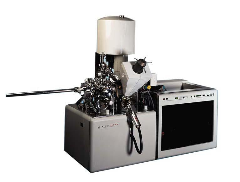
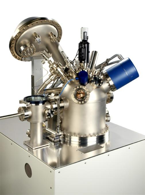
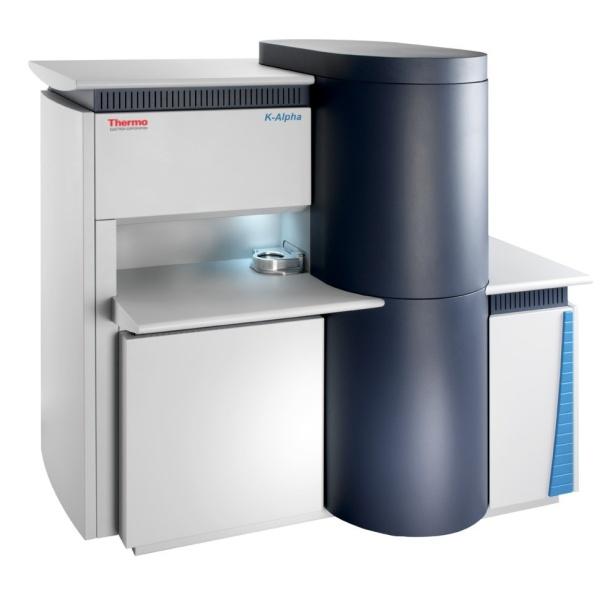
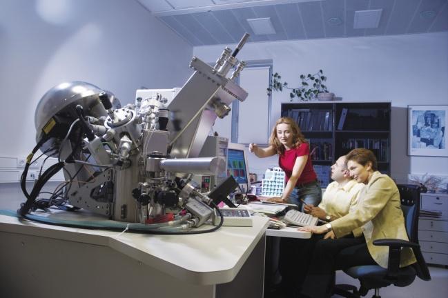
8 Examples of XPS spectrometers 8


9 Instrument: Kratos Axis Ultra DLD Analyser e - Detector e - Monochromator X-ray source X-ray source Sample 9
 Sputter profiles Mapping possible up to full size of sample holder ISS included Target applications Thickness measurements Surface")
10 Instrument: Theta Probe Spectroscopy Source-defined small area XPS 15 µm to 400 µm Snapshot spectrum acquisition Up to 112 channels Faster serial mapping Faster profiling Unique parallel ARXPS with up to 96 channels Large samples (70 mm x 70 mm x 25 mm) Sputter profiles Mapping possible up to full size of sample holder ISS included Target applications Thickness measurements Surface modification, plasma & chemical Self assembly Nanotechnology Ultra thin film technologies Shallow interfaces 10
11 Sample requirements Has to withstand high vacuum ( 10-7 Torr). Has to withstand irradiation by X-rays Sample surface must be clean! Reasonably sized. 11
12 XPS Depth of Analysis The probability that a photoelectron will escape from the sample without losing energy is regulated by the Beer-Lambert law: Where λ e is the photoelectron inelastic mean free path Attenuation length (λ) 0.9 IMFP IMFP: The average distance an electron with a given energy travels between successive inelastic collisions 12
13 Primary structure Features of the XPS spectrum - Core level photoelectron peaks (atom excitation) - Valence band spectra - CCC, CCV, CVV Auger peaks (atom de-excitation) Secondary structure - X-ray satellites and ghosts - Shake up and shake off satellites - Plasmon loss features - Background (slope) 13
14 x 10 4 Auger peaks XPS spectrum ITO In 3s In 3s Sn 3p In 3p Sn 3d O 1s In 3d Photoelectron peaks CPS Sn MNN In MNN In/Sn 4s 20 O KLL C 1s In/Sn 4p Binding Energy (ev) 14
15 Peak width (ΔE) ΔE = (ΔE n2 + ΔE p2 + ΔE a2 ) 1/2 Gaussian broadening: Natural width X-ray source contribution Analyser contribution -Instrumental: There is no perfectly resolving spectrometer nor a perfectly monochromatic X-ray source. -Sample For semiconductor surfaces in particular, variations in the defect density across the surface will lead to variations in the band bending and, thus, the work function will vary from point to point. This variation in surface potential produces a broadening of the XPS peaks. -Excitation process such as the shake-up/shake-off processes or vibrational broadening. Lorentzian broadening. The core-hole that the incident photon creates has a particular lifetime (τ) which is dependent on how quickly the hole is filled by an electron from another shell. From Heisenberg s uncertainty principle, the finite lifetime will produce a broadening of the peak. Γ=h/τ Intrinsic width of the same energy level should increase with increasing atomic number 15
16 Chemical shift ΔE (i) = kδq + ΔV M ΔR Initial state contribution final state contribution Δq: changes in valence charge ΔV M : Coulomb interaction between the photoelectron (i) and the surrounding charged atoms. ΔR: relaxation energy change arising from the response of the atomic environment (local electronic structure) to the screening of the core hole. 16


17 Chemical shift - Growth of ITO on p c-si Intensity arbitrary units Si In oxide Sn oxide Si 2p In 3d 5/2 Sn 3d 5/2 3/2 In 3/2 SiO x 1.5 nm 1.5 nm 1.5 nm 0.5 nm BHF 15 sec o C 3.0 nm Sn 3.0 nm 0.5 nm 0.5 nm Binding Energy (ev) 17
18 Quantification Unlike AES, SIMS, EDX, WDX there are little in the way of matrix effects to worry about in XPS. We can use either theoretical or empirical cross sections, corrected for transmission function of the analyser. In principle the following equation can be used: I = J ρ σ K λ I is the electron intensity J is the photon flux, ρ is the concentration of the atom or ion in the solid, σ s is the cross-section for photoelectron production (which depends on the element and energy being considered), K is a term which covers instrumental factors, λ is the electron attenuation length. In practice atomic sensitivity factors (F) are often used: [A] atomic % = {(IA/FA)/Σ(I/F)} Various compilations are available. 18
19 Chemical shift 19

20 Spin-Orbit Coupling/Splitting Ti oxide 2p 2p 3/2 Arbitrary Units 2p 1/2 The intensity of the peaks is given by the degeneracy g J = 2j Binding Energy (ev) Spin-orbit coupling/ splitting: final state effect for orbitals with orbital angular momentum l> 0. A magnetic interaction between an electron s spin and its orbital angular momentum. Example Ti. Upon photoemission an electron from the p orbital is removed - remaining electron can adopt one of two configurations: a spin-up (s=+1/2) or spin-down (s=-1/2) state. If no spin-orbit interaction these two states would have equal energy (degenerated states). spin-orbit coupling lifts the degeneracy To realise that we need to consider the quantum number, j, the total angular momentum quantum number. j=l + s where s is the spin quantum number (±½). For a p orbital j=1/2 or 3/2. Thus the final state of the system may be either p1/2 or p3/2 and this gives rise to a splitting of the core-level into a doublet as shown in the figure above. Spin-orbit coupling is described for light elements by the Russell-Saunders (LS) coupling approximation and by the j-j coupling approximation for heavier elements 20
21 Plasmons They describe the interaction (inelastic scattering) of the PE with the plasma oscillation of the outer shell (valence band) electrons Plasmons in their quantum mechanical description are pseudoparticles with energy E p =hω ω = (ne 2 /ε 0 m) 1/2 /2π n =valence electron density, e, m electron charge and mass ε 0 =dielectric constant of vacuum Pure elements Mo-Si-Al Compound 21
22 Peak asymmetry Zn Arbitrary Units ZnO Binding Energy (ev) ZnO Zn Arbitrary Units Binding Energy (ev) Peak asymmetry in metals caused by small energy electron-hole excitations near E F of metal


23 Depth profile with ion sputtering SnO 2 Sn Use of an ion gun to erode the sample surface and re-analyse Enables layered structures to be investigated Investigations of interfaces Depth resolution improved by: Low beam energies Small ion beam sizes Sample rotation Depth 23
 λ=attenuation length (λ 0.9 IMFP) λ=538α A /E A2 +0.41α A (α A E A ) 0.")
24 Angle Resolved XPS (ARXPS) for non-destructive depth profile OH oxide I (d) = I o* exp(-d/λ) RT θ I (d) = I o* exp(-d/λcos θ) surface Substrate Film Arbitrary Units AR bulk Binding Energy (ev) λ=attenuation length (λ 0.9 IMFP) λ=538α A /E A α A (α A E A ) 0.5 (α A3 volume of atom, E A electron energy) 24
25 XPS-Check list Depth of analysis ~ 5nm All elements except H and He Readily quantified (limit ca. 0.1 at%) All materials (vacuum compatible) Chemical/electronic state information -Identification of chemical states -Reflection of electronic changes to the atomic potential Compositional depth profiling by -ARXPS (ultra thin film <10 nm), -change of the excitation energy -choose of different spectral areas -sputtering Ultra thin film thickness measurement Analysis area mm 2 to 10 micrometres 25
 d: SiOx film thickness λ Si :inelastic mean free path for Si, Θ: the angle of emission, R: the Si 2p")
26 Interfacial studies of Al 2 O 3 deposited on 4H-SiC(0001) Avice, Diplas, Thøgersen, Christensen, Grossner, Svensson, Nilsen, Fjellvåg, Watts Appl. Physics Letters, 2007;91, 52907, Surface & Interface Analysis,2008;40,822 d=λ Si cosθ ln(1+r/r ) d: SiOx film thickness λ Si :inelastic mean free path for Si, Θ: the angle of emission, R: the Si 2p intensity ratios ISiox/ISiC, R the Si 2p intensity ratios I Siox/I SiC where I is the intensity from an infinitely thick substrate. R =(σ Si,SiO 2. λ Si,SiO 2 ) / (σ Si, Si. λ Si,Si ) where σ Si,SiO2 and λ Si,SiO2 are the number of Si atoms per SiO 2 unit volume and the inelastic mean free path respectively The σ Si,SiO2 / σ Si,Si ratio is given by σ Si,SiO2 / (σ Si,Si = (D SiO2. F Si ) / D Si. F SiO2 where D is the density of the material and F the formula weight. Si 4+ Si 3+ SiC/Si 2+ Si + Si 0 Al 2p plasmon contribution Ar 1273 K 60 mins Ar 1273 K 30 mins Ar 1273 K 15 mins, N2/H2 873 K 30 mins N2/H2 873 K 15 mins as-grown For the calculations we also assumed that the Si 2p photoelectrons from both SiC and Si oxide film will be attenuated by the same amount as they travel through the Al2O3 film therefore, their intensity ratio will reflect the attenuation of the Si 2p electrons coming from the SiC through the Si oxide film. Al 2 O 3 From XPS SiO x d= 1nm at RT, d=3nm at 1273 K SiC 26
 Thin-film stack on glass Mo and Zn oxide layer form electrical contacts p-type CIGS film (sunlight absorber) and n-type CdS film form p-n junction Excellent efficiency Acknowledgement:")
 XPS solution XPS sputter depth profiling Elemental and composition information as a function of depth Identify chemical gradients within layers Investigate chemistry at layer")
27 CIGS solar cell Introduction 3 SEM of a Cu(In,Ga)Se 2 solar cell (cross-section) and its mode of operation CIGS solar cell Energy/environmental application Solar cells based on Cu(In, Ga)Se 2 (CIGS) Thin-film stack on glass Mo and Zn oxide layer form electrical contacts p-type CIGS film (sunlight absorber) and n-type CdS film form p-n junction Excellent efficiency Acknowledgement: Thermo Electron Corporation Low cost compared to thicker silicon-based solar cells Practical problem Controlling film composition and interfacial chemistry between layers (affects electrical properties) XPS solution XPS sputter depth profiling Elemental and composition information as a function of depth Identify chemical gradients within layers Investigate chemistry at layer interfaces 27


28 CIGS solar cell CIGS solar cell Mo Depth profile of CIGS film stack Depth profile of CIFS film stack Demonstrates standardless quantification of XPS Excellent quantification agreement between XPS and Rutherford BackScattering (RBS) Both techniques show cross-over of In and Ga close to 1.6µm depth XPS tool is able to analyze product solar cell device Zn Se O CdS In Cu C Ga Sputter depth profile of CIGS film stack Rutherford BackScatter profile of CIGS film stack 28 Acknowledgement: Thermo Electron Corporation


29 Elemental distribution and oxygen deficiency of magnetron sputtered ITO films A. Thøgersen, M.Rein, E. Monakhov, J. Mayandi, S. Diplas JOURNAL OF APPLIED PHYSICS 109, (2011) 29
X-ray photoelectron spectroscopy - An introduction
 X-ray photoelectron spectroscopy - An introduction Spyros Diplas SINTEF Materials & Chemistry, Sector of Materials and Nanotechnology, Department of Materials Physics-Oslo & Centre of Materials Science
IV. Surface analysis for chemical state, chemical composition
 IV. Surface analysis for chemical state, chemical composition Probe beam Detect XPS Photon (X-ray) Photoelectron(core level electron) UPS Photon (UV) Photoelectron(valence level electron) AES electron
Birck Nanotechnology Center XPS: X-ray Photoelectron Spectroscopy ESCA: Electron Spectrometer for Chemical Analysis
 Birck Nanotechnology Center XPS: X-ray Photoelectron Spectroscopy ESCA: Electron Spectrometer for Chemical Analysis Dmitry Zemlyanov Birck Nanotechnology Center, Purdue University Outline Introduction
An Introduction to Auger Electron Spectroscopy
 An Introduction to Auger Electron Spectroscopy Spyros Diplas MENA3100 SINTEF Materials & Chemistry, Department of Materials Physics & Centre of Materials Science and Nanotechnology, Department of Chemistry,
X-Ray Photoelectron Spectroscopy (XPS)-2
-2") X-Ray Photoelectron Spectroscopy (XPS)-2 Louis Scudiero http://www.wsu.edu/~scudiero; 5-2669 Fulmer 261A Electron Spectroscopy for Chemical Analysis (ESCA) The 3 step model: 1.Optical excitation 2.Transport
X-Ray Photoelectron Spectroscopy (XPS)-2 Louis Scudiero http://www.wsu.edu/~scudiero; 5-2669 Fulmer 261A Electron Spectroscopy for Chemical Analysis (ESCA) The 3 step model: 1.Optical excitation 2.Transport
Electron Spectroscopy
 Electron Spectroscopy Photoelectron spectroscopy is based upon a single photon in/electron out process. The energy of a photon is given by the Einstein relation : E = h ν where h - Planck constant ( 6.62
Introduction to X-ray Photoelectron Spectroscopy (XPS) XPS which makes use of the photoelectric effect, was developed in the mid-1960
 XPS which makes use of the photoelectric effect, was developed in the mid-1960") Introduction to X-ray Photoelectron Spectroscopy (XPS) X-ray Photoelectron Spectroscopy (XPS), also known as Electron Spectroscopy for Chemical Analysis (ESCA) is a widely used technique to investigate
Introduction to X-ray Photoelectron Spectroscopy (XPS) X-ray Photoelectron Spectroscopy (XPS), also known as Electron Spectroscopy for Chemical Analysis (ESCA) is a widely used technique to investigate
X-Ray Photoelectron Spectroscopy (XPS)-2
-2") X-Ray Photoelectron Spectroscopy (XPS)-2 Louis Scudiero http://www.wsu.edu/~pchemlab ; 5-2669 Fulmer 261A Electron Spectroscopy for Chemical Analysis (ESCA) The 3 step model: 1.Optical excitation 2.Transport
X-Ray Photoelectron Spectroscopy (XPS)-2 Louis Scudiero http://www.wsu.edu/~pchemlab ; 5-2669 Fulmer 261A Electron Spectroscopy for Chemical Analysis (ESCA) The 3 step model: 1.Optical excitation 2.Transport
Lecture 5. X-ray Photoemission Spectroscopy (XPS)
") Lecture 5 X-ray Photoemission Spectroscopy (XPS) 5. Photoemission Spectroscopy (XPS) 5. Principles 5.2 Interpretation 5.3 Instrumentation 5.4 XPS vs UV Photoelectron Spectroscopy (UPS) 5.5 Auger Electron
Lecture 5 X-ray Photoemission Spectroscopy (XPS) 5. Photoemission Spectroscopy (XPS) 5. Principles 5.2 Interpretation 5.3 Instrumentation 5.4 XPS vs UV Photoelectron Spectroscopy (UPS) 5.5 Auger Electron
X-ray Photoelectron Spectroscopy (XPS)
") X-ray Photoelectron Spectroscopy (XPS) As part of the course Characterization of Catalysts and Surfaces Prof. Dr. Markus Ammann Paul Scherrer Institut markus.ammann@psi.ch Resource for further reading:
X-ray Photoelectron Spectroscopy (XPS) As part of the course Characterization of Catalysts and Surfaces Prof. Dr. Markus Ammann Paul Scherrer Institut markus.ammann@psi.ch Resource for further reading:
Auger Electron Spectroscopy
 Auger Electron Spectroscopy Auger Electron Spectroscopy is an analytical technique that provides compositional information on the top few monolayers of material. Detect all elements above He Detection
Methods of surface analysis
 Methods of surface analysis Nanomaterials characterisation I RNDr. Věra Vodičková, PhD. Surface of solid matter: last monoatomic layer + absorbed monolayer physical properties are effected (crystal lattice
Photoelectron Peak Intensities in Solids
 Photoelectron Peak Intensities in Solids Electronic structure of solids Photoelectron emission through solid Inelastic scattering Other excitations Intrinsic and extrinsic Shake-up, shake-down and shake-off
Lecture 17 Auger Electron Spectroscopy
 Lecture 17 Auger Electron Spectroscopy Auger history cloud chamber Although Auger emission is intense, it was not used until 1950 s. Evolution of vacuum technology and the application of Auger Spectroscopy
X-Ray Photoelectron Spectroscopy (XPS) Prof. Paul K. Chu
 Prof. Paul K. Chu") X-Ray Photoelectron Spectroscopy (XPS) Prof. Paul K. Chu X-ray Photoelectron Spectroscopy Introduction Qualitative analysis Quantitative analysis Charging compensation Small area analysis and XPS imaging
X-Ray Photoelectron Spectroscopy (XPS) Prof. Paul K. Chu X-ray Photoelectron Spectroscopy Introduction Qualitative analysis Quantitative analysis Charging compensation Small area analysis and XPS imaging
5) Surface photoelectron spectroscopy. For MChem, Spring, Dr. Qiao Chen (room 3R506) University of Sussex.
 Surface photoelectron spectroscopy. For MChem, Spring, Dr. Qiao Chen (room 3R506) University of Sussex.") For MChem, Spring, 2009 5) Surface photoelectron spectroscopy Dr. Qiao Chen (room 3R506) http://www.sussex.ac.uk/users/qc25/ University of Sussex Today s topics 1. Element analysis with XPS Binding energy,
For MChem, Spring, 2009 5) Surface photoelectron spectroscopy Dr. Qiao Chen (room 3R506) http://www.sussex.ac.uk/users/qc25/ University of Sussex Today s topics 1. Element analysis with XPS Binding energy,
Photon Interaction. Spectroscopy
 Photon Interaction Incident photon interacts with electrons Core and Valence Cross Sections Photon is Adsorbed Elastic Scattered Inelastic Scattered Electron is Emitted Excitated Dexcitated Stöhr, NEXAPS
Electron Spettroscopies
 Electron Spettroscopies Spettroscopy allows to characterize a material from the point of view of: chemical composition, electronic states and magnetism, electronic, roto-vibrational and magnetic excitations.
X-Ray Photoelectron Spectroscopy (XPS) Auger Electron Spectroscopy (AES)
 Auger Electron Spectroscopy (AES)") X-Ray Photoelectron Spectroscopy (XPS) Auger Electron Spectroscopy (AES) XPS X-ray photoelectron spectroscopy (XPS) is one of the most used techniques to chemically characterize the surface. Also known
X-Ray Photoelectron Spectroscopy (XPS) Auger Electron Spectroscopy (AES) XPS X-ray photoelectron spectroscopy (XPS) is one of the most used techniques to chemically characterize the surface. Also known
X- ray Photoelectron Spectroscopy and its application in phase- switching device study
 X- ray Photoelectron Spectroscopy and its application in phase- switching device study Xinyuan Wang A53073806 I. Background X- ray photoelectron spectroscopy is of great importance in modern chemical and
Lecture 20 Auger Electron Spectroscopy
 Lecture 20 Auger Electron Spectroscopy Auger history cloud chamber Although Auger emission is intense, it was not used until 1950 s. Evolution of vacuum technology and the application of Auger Spectroscopy
Dr. Tim Nunney Thermo Fisher Scientific, East Grinstead, UK Dr. Nick Bulloss Thermo Fisher Scientific, Madison, WI, USA Dr. Harry Meyer III Oak Ridge
 Dr. Tim Nunney Thermo Fisher Scientific, East Grinstead, UK Dr. Nick Bulloss Thermo Fisher Scientific, Madison, WI, USA Dr. Harry Meyer III Oak Ridge National Laboratory, TN, USA Introduction New materials
Auger Electron Spectroscopy Overview
 Auger Electron Spectroscopy Overview Also known as: AES, Auger, SAM 1 Auger Electron Spectroscopy E KLL = E K - E L - E L AES Spectra of Cu EdN(E)/dE Auger Electron E N(E) x 5 E KLL Cu MNN Cu LMM E f E
5.8 Auger Electron Spectroscopy (AES)
") 5.8 Auger Electron Spectroscopy (AES) 5.8.1 The Auger Process X-ray and high energy electron bombardment of atom can create core hole Core hole will eventually decay via either (i) photon emission (x-ray
5.8 Auger Electron Spectroscopy (AES) 5.8.1 The Auger Process X-ray and high energy electron bombardment of atom can create core hole Core hole will eventually decay via either (i) photon emission (x-ray
Lecture 12 Multiplet splitting
 Lecture 12 Multiplet splitting Multiplet splitting Atomic various L and S terms Both valence and core levels Rare earths Transition metals Paramagnetic free molecules Consider 3s level emission from Mn2+
MS482 Materials Characterization ( 재료분석 ) Lecture Note 4: XRF
 Lecture Note 4: XRF") 2016 Fall Semester MS482 Materials Characterization ( 재료분석 ) Lecture Note 4: XRF Byungha Shin Dept. of MSE, KAIST 1 Course Information Syllabus 1. Overview of various characterization techniques (1 lecture)
2016 Fall Semester MS482 Materials Characterization ( 재료분석 ) Lecture Note 4: XRF Byungha Shin Dept. of MSE, KAIST 1 Course Information Syllabus 1. Overview of various characterization techniques (1 lecture)
MSE 321 Structural Characterization
 Auger Spectroscopy Auger Electron Spectroscopy (AES) Scanning Auger Microscopy (SAM) Incident Electron Ejected Electron Auger Electron Initial State Intermediate State Final State Physical Electronics
Advanced Lab Course. X-Ray Photoelectron Spectroscopy 1 INTRODUCTION 1 2 BASICS 1 3 EXPERIMENT Qualitative analysis Chemical Shifts 7
 Advanced Lab Course X-Ray Photoelectron Spectroscopy M210 As of: 2015-04-01 Aim: Chemical analysis of surfaces. Content 1 INTRODUCTION 1 2 BASICS 1 3 EXPERIMENT 3 3.1 Qualitative analysis 6 3.2 Chemical
Theta Probe: A tool for characterizing ultra thin films and self assembled monolayers using parallel angle resolved XPS (ARXPS)
") Theta Probe: A tool for characterizing ultra thin films and self assembled monolayers using parallel angle resolved XPS (ARXPS) C. E. Riley, P. Mack, T. S. Nunney and R. G. White Thermo Fisher Scientific
Theta Probe: A tool for characterizing ultra thin films and self assembled monolayers using parallel angle resolved XPS (ARXPS) C. E. Riley, P. Mack, T. S. Nunney and R. G. White Thermo Fisher Scientific
Auger Electron Spectroscopy (AES)
") 1. Introduction Auger Electron Spectroscopy (AES) Silvia Natividad, Gabriel Gonzalez and Arena Holguin Auger Electron Spectroscopy (Auger spectroscopy or AES) was developed in the late 1960's, deriving
1. Introduction Auger Electron Spectroscopy (AES) Silvia Natividad, Gabriel Gonzalez and Arena Holguin Auger Electron Spectroscopy (Auger spectroscopy or AES) was developed in the late 1960's, deriving
Auger Electron Spectroscopy (AES) Prof. Paul K. Chu
 Prof. Paul K. Chu") Auger Electron Spectroscopy (AES) Prof. Paul K. Chu Auger Electron Spectroscopy Introduction Principles Instrumentation Qualitative analysis Quantitative analysis Depth profiling Mapping Examples The Auger
Auger Electron Spectroscopy (AES) Prof. Paul K. Chu Auger Electron Spectroscopy Introduction Principles Instrumentation Qualitative analysis Quantitative analysis Depth profiling Mapping Examples The Auger
MS482 Materials Characterization ( 재료분석 ) Lecture Note 2: UPS
 Lecture Note 2: UPS") 2016 Fall Semester MS482 Materials Characterization ( 재료분석 ) Lecture Note 2: UPS Byungha Shin Dept. of MSE, KAIST 1 Course Information Syllabus 1. Overview of various characterization techniques (1 lecture)
2016 Fall Semester MS482 Materials Characterization ( 재료분석 ) Lecture Note 2: UPS Byungha Shin Dept. of MSE, KAIST 1 Course Information Syllabus 1. Overview of various characterization techniques (1 lecture)
Auger Electron Spectrometry. EMSE-515 F. Ernst
 Auger Electron Spectrometry EMSE-515 F. Ernst 1 Principle of AES electron or photon in, electron out radiation-less transition Auger electron electron energy properties of atom 2 Brief History of Auger
8.6 Relaxation Processes
 CHAPTER 8. INNER SHELLS 175 Figure 8.17: Splitting of the 3s state in Fe which is missing in Zn. Refs. [12,13]. be aligned parallel or antiparallel with the spins of the 3d electrons of iron. 13 Thus we
XPS & Scanning Auger Principles & Examples
 XPS & Scanning Auger Principles & Examples Shared Research Facilities Lunch Talk Contact info: dhu Pujari & Han Zuilhof Lab of rganic Chemistry Wageningen University E-mail: dharam.pujari@wur.nl Han.Zuilhof@wur.nl
Ultraviolet Photoelectron Spectroscopy (UPS)
") Ultraviolet Photoelectron Spectroscopy (UPS) Louis Scudiero http://www.wsu.edu/~scudiero www.wsu.edu/~scudiero; ; 5-26695 scudiero@wsu.edu Photoemission from Valence Bands Photoelectron spectroscopy is
Ultraviolet Photoelectron Spectroscopy (UPS) Louis Scudiero http://www.wsu.edu/~scudiero www.wsu.edu/~scudiero; ; 5-26695 scudiero@wsu.edu Photoemission from Valence Bands Photoelectron spectroscopy is
Name: (a) What core levels are responsible for the three photoelectron peaks in Fig. 1?
 What core levels are responsible for the three photoelectron peaks in Fig. 1?") Physics 243A--Surface Physics of Materials: Spectroscopy Final Examination December 16, 2014 (3 problems, 100 points total, open book, open notes and handouts) Name: [1] (50 points), including Figures
Physics 243A--Surface Physics of Materials: Spectroscopy Final Examination December 16, 2014 (3 problems, 100 points total, open book, open notes and handouts) Name: [1] (50 points), including Figures
Lecture 11 Surface Characterization of Biomaterials in Vacuum
 1 Lecture 11 Surface Characterization of Biomaterials in Vacuum The structure and chemistry of a biomaterial surface greatly dictates the degree of biocompatibility of an implant. Surface characterization
Auger Electron Spectroscopy *
 OpenStax-CNX module: m43546 1 Auger Electron Spectroscopy * Amanda M. Goodman Andrew R. Barron This work is produced by OpenStax-CNX and licensed under the Creative Commons Attribution License 3.0 1 Basic
QUESTIONS AND ANSWERS
 QUESTIONS AND ANSWERS (1) For a ground - state neutral atom with 13 protons, describe (a) Which element this is (b) The quantum numbers, n, and l of the inner two core electrons (c) The stationary state
Lecture 22 Ion Beam Techniques
 Lecture 22 Ion Beam Techniques Schroder: Chapter 11.3 1/44 Announcements Homework 6/6: Will be online on later today. Due Wednesday June 6th at 10:00am. I will return it at the final exam (14 th June).
Photoemission Spectroscopy
 FY13 Experimental Physics - Auger Electron Spectroscopy Photoemission Spectroscopy Supervisor: Per Morgen SDU, Institute of Physics Campusvej 55 DK - 5250 Odense S Ulrik Robenhagen,
MS482 Materials Characterization ( 재료분석 ) Lecture Note 5: RBS
 Lecture Note 5: RBS") 2016 Fall Semester MS482 Materials Characterization ( 재료분석 ) Lecture Note 5: RBS Byungha Shin Dept. of MSE, KAIST 1 Course Information Syllabus 1. Overview of various characterization techniques (1 lecture)
2016 Fall Semester MS482 Materials Characterization ( 재료분석 ) Lecture Note 5: RBS Byungha Shin Dept. of MSE, KAIST 1 Course Information Syllabus 1. Overview of various characterization techniques (1 lecture)
Energy Spectroscopy. Excitation by means of a probe
 Energy Spectroscopy Excitation by means of a probe Energy spectral analysis of the in coming particles -> XAS or Energy spectral analysis of the out coming particles Different probes are possible: Auger
PHOTOELECTRON SPECTROSCOPY (PES)
") PHOTOELECTRON SPECTROSCOPY (PES) NTRODUCTON Law of Photoelectric effect Albert Einstein, Nobel Prize 1921 Kaiser-Wilhelm-nstitut (now Max-Planck- nstitut) für Physik Berlin, Germany High-resolution electron
PHOTOELECTRON SPECTROSCOPY (PES) NTRODUCTON Law of Photoelectric effect Albert Einstein, Nobel Prize 1921 Kaiser-Wilhelm-nstitut (now Max-Planck- nstitut) für Physik Berlin, Germany High-resolution electron
Lecture 10. Transition probabilities and photoelectric cross sections
 Lecture 10 Transition probabilities and photoelectric cross sections TRANSITION PROBABILITIES AND PHOTOELECTRIC CROSS SECTIONS Cross section = = Transition probability per unit time of exciting a single
The Benefit of Wide Energy Range Spectrum Acquisition During Sputter Depth Profile Measurements
 The Benefit of Wide Energy Range Spectrum Acquisition During Sputter Depth Profile Measurements Uwe Scheithauer, 82008 Unterhaching, Germany E-Mail: scht.uhg@googlemail.com Internet: orcid.org/0000-0002-4776-0678;
The Use of Synchrotron Radiation in Modern Research
 The Use of Synchrotron Radiation in Modern Research Physics Chemistry Structural Biology Materials Science Geochemical and Environmental Science Atoms, molecules, liquids, solids. Electronic and geometric
Lecture 7 Chemical/Electronic Structure of Glass
 Lecture 7 Chemical/Electronic Structure of Glass Syllabus Topic 6. Electronic spectroscopy studies of glass structure Fundamentals and Applications of X-ray Photoelectron Spectroscopy (XPS) a.k.a. Electron
Lecture 23 X-Ray & UV Techniques
 Lecture 23 X-Ray & UV Techniques Schroder: Chapter 11.3 1/50 Announcements Homework 6/6: Will be online on later today. Due Wednesday June 6th at 10:00am. I will return it at the final exam (14 th June).
Application of Surface Analysis for Root Cause Failure Analysis
 Application of Surface Analysis for Root Cause Failure Analysis David A. Cole Evans Analytical Group East Windsor, NJ Specialists in Materials Characterization Outline Introduction X-Ray Photoelectron
Secondary Ion Mass Spectrometry (SIMS)
") CHEM53200: Lecture 10 Secondary Ion Mass Spectrometry (SIMS) Major reference: Surface Analysis Edited by J. C. Vickerman (1997). 1 Primary particles may be: Secondary particles can be e s, neutral species
CHEM53200: Lecture 10 Secondary Ion Mass Spectrometry (SIMS) Major reference: Surface Analysis Edited by J. C. Vickerman (1997). 1 Primary particles may be: Secondary particles can be e s, neutral species
Extraction of Depth Information from ARXPS Data
 The world leader in serving science Extraction of Depth Information from ARXPS Data John Wolstenholme Theta Probe Features X-ray monochromator with spot size from 15 µm to 4 µm Real time angle resolved
X-Ray Photoelectron Spectroscopy (XPS)
") X-Ray Photoelectron Spectroscopy (XPS) Louis Scudiero http://www.wsu.edu/~scudiero; 5-2669 Electron Spectroscopy for Chemical Analysis (ESCA) The basic principle of the photoelectric effect was enunciated
X-Ray Photoelectron Spectroscopy (XPS) Louis Scudiero http://www.wsu.edu/~scudiero; 5-2669 Electron Spectroscopy for Chemical Analysis (ESCA) The basic principle of the photoelectric effect was enunciated
Solid Surfaces, Interfaces and Thin Films
 Hans Lüth Solid Surfaces, Interfaces and Thin Films Fifth Edition With 427 Figures.2e Springer Contents 1 Surface and Interface Physics: Its Definition and Importance... 1 Panel I: Ultrahigh Vacuum (UHV)
ToF-SIMS or XPS? Xinqi Chen Keck-II
 ToF-SIMS or XPS? Xinqi Chen Keck-II 1 Time of Flight Secondary Ion Mass Spectrometry (ToF-SIMS) Not ToF MS (laser, solution) X-ray Photoelectron Spectroscopy (XPS) 2 3 Modes of SIMS 4 Secondary Ion Sputtering
Chemical Analysis in TEM: XEDS, EELS and EFTEM. HRTEM PhD course Lecture 5
 Chemical Analysis in TEM: XEDS, EELS and EFTEM HRTEM PhD course Lecture 5 1 Part IV Subject Chapter Prio x-ray spectrometry 32 1 Spectra and mapping 33 2 Qualitative XEDS 34 1 Quantitative XEDS 35.1-35.4
Reduced preferential sputtering of TiO 2 (and Ta 2 O 5 ) thin films through argon cluster ion bombardment.
 thin films through argon cluster ion bombardment.") NATIOMEM Reduced preferential sputtering of TiO 2 (and Ta 2 O 5 ) thin films through argon cluster ion bombardment. R. Grilli *, P. Mack, M.A. Baker * * University of Surrey, UK ThermoFisher Scientific
NATIOMEM Reduced preferential sputtering of TiO 2 (and Ta 2 O 5 ) thin films through argon cluster ion bombardment. R. Grilli *, P. Mack, M.A. Baker * * University of Surrey, UK ThermoFisher Scientific
MSE 321 Structural Characterization
 Auger Spectroscopy Auger Electron Spectroscopy (AES) Scanning Auger Microscopy (SAM) Incident Electron Ejected Electron Auger Electron Initial State Intermediate State Final State Physical Electronics
The design of an integrated XPS/Raman spectroscopy instrument for co-incident analysis
 The design of an integrated XPS/Raman spectroscopy instrument for co-incident analysis Tim Nunney The world leader in serving science 2 XPS Surface Analysis XPS +... UV Photoelectron Spectroscopy UPS He(I)
1 Introduction COPYRIGHTED MATERIAL. 1.1 HowdoweDefinetheSurface?
 1 Introduction JOHN C. VICKERMAN Manchester Interdisciplinary Biocentre, School of Chemical Engineering and Analytical Science, The University of Manchester, Manchester, UK The surface behaviour of materials
X-Ray Photoelectron Spectroscopy: Theory and Practice
 X-Ray Photoelectron Spectroscopy: Theory and Practice PHYS-581 (Fall 2010) Contact Information for EMS in RRC-East Alan Nicholls, PhD Director of Research Service Facility - Electron Microscopy Research
X-ray Spectroscopy. Interaction of X-rays with matter XANES and EXAFS XANES analysis Pre-edge analysis EXAFS analysis
 X-ray Spectroscopy Interaction of X-rays with matter XANES and EXAFS XANES analysis Pre-edge analysis EXAFS analysis Element specific Sensitive to low concentrations (0.01-0.1 %) Why XAS? Applicable under
Inelastic soft x-ray scattering, fluorescence and elastic radiation
 Inelastic soft x-ray scattering, fluorescence and elastic radiation What happens to the emission (or fluorescence) when the energy of the exciting photons changes? The emission spectra (can) change. One
Photoelectron spectroscopy Instrumentation. Nanomaterials characterization 2
 Photoelectron spectroscopy Instrumentation Nanomaterials characterization 2 RNDr. Věra V Vodičkov ková,, PhD. Photoelectron Spectroscopy general scheme Impact of X-ray emitted from source to the sample
Surface analysis techniques
 Experimental methods in physics Surface analysis techniques 3. Ion probes Elemental and molecular analysis Jean-Marc Bonard Academic year 10-11 3. Elemental and molecular analysis 3.1.!Secondary ion mass
Photoelectron Spectroscopy
 Stefan Hüfner Photoelectron Spectroscopy Principles and Applications Third Revised and Enlarged Edition With 461 Figures and 28 Tables JSJ Springer ... 1. Introduction and Basic Principles 1 1.1 Historical
MS482 Materials Characterization ( 재료분석 ) Lecture Note 5: RBS. Byungha Shin Dept. of MSE, KAIST
 Lecture Note 5: RBS. Byungha Shin Dept. of MSE, KAIST") 2015 Fall Semester MS482 Materials Characterization ( 재료분석 ) Lecture Note 5: RBS Byungha Shin Dept. of MSE, KAIST 1 Course Information Syllabus 1. Overview of various characterization techniques (1 lecture)
2015 Fall Semester MS482 Materials Characterization ( 재료분석 ) Lecture Note 5: RBS Byungha Shin Dept. of MSE, KAIST 1 Course Information Syllabus 1. Overview of various characterization techniques (1 lecture)
Applications of XPS, AES, and TOF-SIMS
 Applications of XPS, AES, and TOF-SIMS Scott R. Bryan Physical Electronics 1 Materials Characterization Techniques Microscopy Optical Microscope SEM TEM STM SPM AFM Spectroscopy Energy Dispersive X-ray
Lecture 3: Optical Properties of Insulators, Semiconductors, and Metals. 5 nm
 Metals Lecture 3: Optical Properties of Insulators, Semiconductors, and Metals 5 nm Course Info Next Week (Sept. 5 and 7) no classes First H/W is due Sept. 1 The Previous Lecture Origin frequency dependence
Core Level Spectroscopies
 Core Level Spectroscopies Spectroscopies involving core levels are element-sensitive, and that makes them very useful for understanding chemical bonding, as well as for the study of complex materials.
ATOMIC STRUCTURE, ELECTRONS, AND PERIODICITY
 ATOMIC STRUCTURE, ELECTRONS, AND PERIODICITY All matter is made of atoms. There are a limited number of types of atoms; these are the elements. (EU 1.A) Development of Atomic Theory Atoms are so small
Half-Integer Quantum Conductance States
 Supporting Information A 50 mv Cu/SiO /W Memristor with Half-Integer Quantum Conductance States S. R. Nandakumar, Marie Minvielle, Saurabh Nagar, Catherine Dubourdieu, and Bipin Rajendran, Department of
X-ray Photoemission Spectroscopy (XPS - Ma4)
") Master Laboratory Report X-ray Photoemission Spectroscopy (XPS - Ma4) Supervisor: Andrew Britton Students: Dachi Meurmishvili, Muhammad Khurram Riaz and Martin Borchert Date: November 17th 2016 1 Contents
Master Laboratory Report X-ray Photoemission Spectroscopy (XPS - Ma4) Supervisor: Andrew Britton Students: Dachi Meurmishvili, Muhammad Khurram Riaz and Martin Borchert Date: November 17th 2016 1 Contents
Interaction of particles with matter - 2. Silvia Masciocchi, GSI and University of Heidelberg SS2017, Heidelberg May 3, 2017
 Interaction of particles with matter - 2 Silvia Masciocchi, GSI and University of Heidelberg SS2017, Heidelberg May 3, 2017 Energy loss by ionization (by heavy particles) Interaction of electrons with
Surface Analysis - The Principal Techniques
 Surface Analysis - The Principal Techniques Edited by John C. Vickerman Surface Analysis Research Centre, Department of Chemistry UMIST, Manchester, UK JOHN WILEY & SONS Chichester New York Weinheim Brisbane
Review of Optical Properties of Materials
 Review of Optical Properties of Materials Review of optics Absorption in semiconductors: qualitative discussion Derivation of Optical Absorption Coefficient in Direct Semiconductors Photons When dealing
Lecture 10. Transition probabilities and photoelectric cross sections
 Lecture 10 Transition probabilities and photoelectric cross sections TRANSITION PROBABILITIES AND PHOTOELECTRIC CROSS SECTIONS Cross section = σ = Transition probability per unit time of exciting a single
X-Ray Photoelectron Spectroscopy (XPS)
") X-Ray Photoelectron Spectroscopy (XPS) Louis Scudiero http://www.wsu.edu/~scudiero; 5-2669 Fulmer 261A Electron Spectroscopy for Chemical Analysis (ESCA) The basic principle of the photoelectric effect
X-Ray Photoelectron Spectroscopy (XPS) Louis Scudiero http://www.wsu.edu/~scudiero; 5-2669 Fulmer 261A Electron Spectroscopy for Chemical Analysis (ESCA) The basic principle of the photoelectric effect
Secondary Ion Mass Spectrometry (SIMS) Thomas Sky
 Thomas Sky") 1 Secondary Ion Mass Spectrometry (SIMS) Thomas Sky Depth (µm) 2 Characterization of solar cells 0,0 1E16 1E17 1E18 1E19 1E20 0,2 0,4 0,6 0,8 1,0 1,2 P Concentration (cm -3 ) Characterization Optimization
1 Secondary Ion Mass Spectrometry (SIMS) Thomas Sky Depth (µm) 2 Characterization of solar cells 0,0 1E16 1E17 1E18 1E19 1E20 0,2 0,4 0,6 0,8 1,0 1,2 P Concentration (cm -3 ) Characterization Optimization
Skoog Chapter 6 Introduction to Spectrometric Methods
 Skoog Chapter 6 Introduction to Spectrometric Methods General Properties of Electromagnetic Radiation (EM) Wave Properties of EM Quantum Mechanical Properties of EM Quantitative Aspects of Spectrochemical
Interaction X-rays - Matter
 Interaction X-rays - Matter Pair production hν > M ev Photoelectric absorption hν MATTER hν Transmission X-rays hν' < hν Scattering hν Decay processes hν f Compton Thomson Fluorescence Auger electrons
Electron Rutherford Backscattering, a versatile tool for the study of thin films
 Electron Rutherford Backscattering, a versatile tool for the study of thin films Maarten Vos Research School of Physics and Engineering Australian National University Canberra Australia Acknowledgements:
Ma5: Auger- and Electron Energy Loss Spectroscopy
 Ma5: Auger- and Electron Energy Loss Spectroscopy 1 Introduction Electron spectroscopies, namely Auger electron- and electron energy loss spectroscopy are utilized to determine the KLL spectrum and the
Auger Analyses Using Low Angle Incident Electrons
 Auger Analyses Using Low Angle Incident Electrons Kenichi Tsutsumi, Yuji agasawa and Toyohiko Tazawa Electron ptics Division, JEL Ltd. Introduction Auger Electron Spectroscopy (AES) is widely used, as
Chemical analysis of surfaces and organic thin films by means of XPS
 Chemical analysis of surfaces and organic thin films by means of XPS X-ray photoelectron spectroscopy The photoelectric effect Wilhelm Hallwachs (1886), Albert Einstein (1905) und Ernest Rutherford (1914)
Fig 1: Auger Electron Generation (a) Step 1 and (b) Step 2
 Step 1 and (b) Step 2") Auger Electron Spectroscopy (AES) Physics of AES: Auger Electrons were discovered in 1925 but were used in surface analysis technique in 1968. Auger Electron Spectroscopy (AES) is a very effective method
Auger Electron Spectroscopy (AES) Physics of AES: Auger Electrons were discovered in 1925 but were used in surface analysis technique in 1968. Auger Electron Spectroscopy (AES) is a very effective method
The Inclusion of Impurities in Graphene Grown on Silicon Carbide
 The Inclusion of Impurities in Graphene Grown on Silicon Carbide Sara Rothwell May 23, 2013 Goal: Experimentally Fabricate Doped Graphene Procedure: 1. Introduce dopant in substrate ImplantaEon NO Process
An Introduction to Diffraction and Scattering. School of Chemistry The University of Sydney
 An Introduction to Diffraction and Scattering Brendan J. Kennedy School of Chemistry The University of Sydney 1) Strong forces 2) Weak forces Types of Forces 3) Electromagnetic forces 4) Gravity Types
ATOMIC STRUCTURE, ELECTRONS, AND PERIODICITY
 ATOMIC STRUCTURE, ELECTRONS, AND PERIODICITY All matter is made of atoms. There are a limited number of types of atoms; these are the elements. (EU 1.A) Development of Atomic Theory Atoms are so small
Characterization of Secondary Emission Materials for Micro-Channel Plates. S. Jokela, I. Veryovkin, A. Zinovev
 Characterization of Secondary Emission Materials for Micro-Channel Plates S. Jokela, I. Veryovkin, A. Zinovev Secondary Electron Yield Testing Technique We have incorporated XPS, UPS, Ar-ion sputtering,
Vacuum Science and Technology in Accelerators
 Vacuum Science and Technology in Accelerators Lectures are the members of ASTeC Vacuum Science Group: Oleg Malyshev (Lectures 1,6) Keith Middleman (Lectures 2,3) Joe Herbert (Lecture 4) Reza Valizadeh
Practical Surface Analysis
 Practical Surface Analysis SECOND EDITION Volume 1 Auger and X-ray Photoelectron Spectroscopy Edited by D. BRIGGS ICI PLC, Wilton Materials Research Centre, Wilton, Middlesbrough, Cleveland, UK and M.
Chap. 3. Elementary Quantum Physics
 Chap. 3. Elementary Quantum Physics 3.1 Photons - Light: e.m "waves" - interference, diffraction, refraction, reflection with y E y Velocity = c Direction of Propagation z B z Fig. 3.1: The classical view
Gaetano L Episcopo. Scanning Electron Microscopy Focus Ion Beam and. Pulsed Plasma Deposition
 Gaetano L Episcopo Scanning Electron Microscopy Focus Ion Beam and Pulsed Plasma Deposition Hystorical background Scientific discoveries 1897: J. Thomson discovers the electron. 1924: L. de Broglie propose
Reflection = EM strikes a boundary between two media differing in η and bounces back
 Reflection = EM strikes a boundary between two media differing in η and bounces back Incident ray θ 1 θ 2 Reflected ray Medium 1 (air) η = 1.00 Medium 2 (glass) η = 1.50 Specular reflection = situation
4. How can fragmentation be useful in identifying compounds? Permits identification of branching not observed in soft ionization.
 Homework 9: Chapters 20-21 Assigned 12 April; Due 17 April 2006; Quiz on 19 April 2006 Chap. 20 (Molecular Mass Spectroscopy) Chap. 21 (Surface Analysis) 1. What are the types of ion sources in molecular
A Beginners Guide to XPS
 A Beginners Guide to XPS XPS Instrumentation Figure 1: Schematic of an XPS instrument. Photoemission occurs when photon energy is transferred to electrons within bound-states of atoms causing the electron
Spectroscopy at nanometer scale
 Spectroscopy at nanometer scale 1. Physics of the spectroscopies 2. Spectroscopies for the bulk materials 3. Experimental setups for the spectroscopies 4. Physics and Chemistry of nanomaterials Various
ECE Semiconductor Device and Material Characterization
 ECE 4813 Semiconductor Device and Material Characterization Dr. Alan Doolittle School of Electrical and Computer Engineering Georgia Institute of Technology As with all of these lecture slides, I am indebted