Dr. Tim Nunney Thermo Fisher Scientific, East Grinstead, UK Dr. Nick Bulloss Thermo Fisher Scientific, Madison, WI, USA Dr. Harry Meyer III Oak Ridge
|
|
|
- Dina Sparks
- 5 years ago
- Views:
Transcription


1 Dr. Tim Nunney Thermo Fisher Scientific, East Grinstead, UK Dr. Nick Bulloss Thermo Fisher Scientific, Madison, WI, USA Dr. Harry Meyer III Oak Ridge National Laboratory, TN, USA


2 Introduction New materials create new characterization challenges Full characterization requires a variety of experimental techniques 2
3 Introduction Techniques need to be chosen that provide complimentary information Elemental and chemical composition Molecular fingerprinting Composition with increasing depth Surface structure Morphology XPS Surface Analysis Microanalysis 3

4 Introduction to X-ray Microanalysis In an electron column, electrons are accelerated through an electric field, acquiring kinetic energy. The energy is transferred to the sample Yields a variety of signals for analysis 4

5 EDS Basic Overview Energy Dispersive X-Ray Spectroscopy (EDX / EDS) Analysis of elemental content of micro-volumes using non-destructive techniques. Based on inner electron transitions between inner atomic shells. Energetic electron from an electron column dislodges an orbital electron. Electron from a higher energy shell fills the vacancy, losing energy in the process. The lost energy appears as emitted radiation of energy (characteristic X-Ray). 5

6 Electron Beam & Sample Interaction Interaction Volume The volume in which the primary electrons interact with a sample As electrons interact with the sample, they are scattered and spread. 6


7 Properties of X-Rays The relationship between Energy, Frequency, and Wavelength may be expressed by one formula E is the Energy of the radiation is the Wavelength of the radiation F is the Frequency of the radiation c is the speed of light 3 x cm/second h is Planck s constant x ev-sec = x erg-sec 7
")
 Collect the full range of")

8 Detectors Energy-dispersive detectors (EDS) Wavelength-dispersive detectors (WDS) Collect the full range of x-ray energies simultaneously Collect one element at a time via a diffracting crystal 8
 Thin films using XPS in combination with sputter profiling Surface (1 nm) 3 atomic")
9 Definition of a surface XPS surface analysis What is a surface? XPS measures Surfaces using XPS and angle resolved XPS Ultra-thin films using XPS and angle resolved XPS (ARXPS) Thin films using XPS in combination with sputter profiling Surface (1 nm) 3 atomic layers The modified layer is often far too thin to be characterized with most techniques. The extreme surface sensitivity of XPS ensures that only the top few nanometers of the sample are analyzed. Bulk Ultra-thin film (1 to 10 nm) 3-30 atomic layers Thin Film (10 nm to 2µm) atomic layers Note: Approximate layer thickness only. Actual values depend upon materials 9

 Analysis of insulating samples Ion gun")

10 XPS instrumentation UHV System Ultra-high vacuum keeps surfaces clean Allows longer photoelectron path length X-ray source Typically Al Ka radiation Monochromated using quartz crystal Low energy electron flood gun Low energy e - (and possibly Ar + ) Analysis of insulating samples Ion gun Typically noble gas ions Sample cleaning Depth profiling Electron transfer lens Flood gun Hemispherical analyser Detector Ion gun Mono crystal X-ray source 10
 Kinetic energy, KE, of photoelectrons is")
11 Basic XPS theory X-rays Photoelectron ejected Binding Kinetic Energy (ev) NaCl Surface is composed of atoms Electrons surround the nucleus of an atom, occupying orbitals at different energies Surface is irradiated with X-rays from a photon source X-rays cause electrons to be ejected (photoelectrons) Kinetic energy, KE, of photoelectrons is measured by an analyser The binding energy, BE, of the electrons is deduced from the kinetic energy and photon energy BE = h -KE Binding energy depends upon Element Orbital from which electron was ejected Chemical state of the element 11
12 Surface analysis and XPS O Elemental identification Which elements are present? Elemental identification Can detect all elements except for H Elemental quantification How much of an element is present? Detection limit >0.05% for most elements Allows determination of stoichiometry Zn 1200 Zn Fe F Ca C Cl S P Element At% P 0.29 S 0.29 Cl 0.22 C Ca O F 1.50 Fe 6.74 Zn 3.03 Mg 0.12 Binding energy / ev Elemental identification of tribology sample 12
13 Surface analysis and XPS Poly(ethylene terephthalate), PET Carbon O C C O C C O O n Elemental identification Which elements are present? Can detect all elements except for H Elemental quantification How much of an element is present? Detection limit >0.05% for most elements Allows determination of stoichiometry Chemical state identification and quantification Bonding states for each element Chemical structure Chemical state identification Binding energy / ev High energy resolution spectroscopy
14 Surface analysis and XPS Poly(ethylene terephthalate), PET Oxygen O C C O C C O O n Elemental identification Which elements are present? Can detect all elements except for H Elemental quantification How much of an element is present? Detection limit >0.05% for most elements Allows determination of stoichiometry Chemical state identification and quantification Bonding states for each element Chemical structure Chemical state identification Binding energy / ev High energy resolution spectroscopy
15 Case Study 1: Membrane electrode assembly
 High conversion efficiency and low/zero pollution Low operating temperature and relatively quick start-up Membrane Electrode")
 sample preparation to allow imaging of nanoscale layers Quantitative elemental and chemical state mapping")
16 MEA fuel cell Introduction Schematic of polymer electrolyte membrane Pt/C Nafion K-Alpha optical image of ULAMprepared MEA fuel cell MEA fuel cell Energy/environmental application Fuel cells for clean conversion of hydrogen 1 Proton exchange membrane fuel cell (PEMFC) High conversion efficiency and low/zero pollution Low operating temperature and relatively quick start-up Membrane Electrode Assembly (MEA) is important component of PEMFC Active layer of platinum/carbon black catalyst with polymeric adjacent layers Practical problem Diffusion of Pt into adjacent polymer layers would reduce Pt/C catalytic effect Solution XPS imaging of sample ULAM (ultra low angle microtomy) sample preparation to allow imaging of nanoscale layers Quantitative elemental and chemical state mapping 16 1 Korean J Chem Eng, 23(4), (2006)
 consists of layers microns thick Thin Pt/C")


17 MEA fuel cell Chemical analysis of Nafion Backscatter image of cross-section of MEA fuel cell component Anode Anode Membrane Cathode Membrane Data points MEA fuel cell Chemical analysis of Nafion Membrane Electrode Assembly (MEA) consists of layers microns thick Thin Pt/C layers around a thicker Nafion layer Nafion is an effective proton exchange membrane Permits hydrogen ion transport while preventing electron conduction Requirement to analyze profile of Pt in Nafion layer Layers are too thick for XPS sputter profiling Not enough data points per layer with standard cross-sectioning Use ultra-low angle microtomy to create crosssection with layers on micron scale 2 Enables XPS mapping and imaging analysis Data points Cathode Backscatter image of ULAM-prepared MEA fuel cell component 17 2 Journal of Materials Science 40 (2005)
18 MEA fuel cell Chemical analysis of Nafion Pt/C Pt/C Nafion ULAM-prepared MEA fuel cell Nafion MEA fuel cell Chemical analysis of Nafion XPS can distinguish carbon bonding states Epoxy (used in making the ULAM cross-section) C-C, C-O and C=O bonding observed Nafion (part of the MEA) CF 2 bonding observed Surface contamination of Nafion gives additional C-C and C-O peaks Epoxy 18


 Pt detected in catalytically active layer At% 80.00 70.00 60.00 Element 50.")
19 MEA fuel cell Elemental quantification of MEA-ULAM sample Pt/C Nafion MEA fuel cell Elemental quantification of MEA-ULAM sample XPS can elementally quantify small areas on a sample Quantification of Pt/C, Nafion and Epoxy zones below Elemental quantification of MEA-ULAM sample ULAM-prepared MEA fuel cell Fluorine observed in Pt/C zones Nafion intentionally mixed with Pt/C during manufacture of catalyst layer Sulfur detected in all regions, principally in Nafion and Pt/C zones XPS is able to detect elements at low concentration (S<0.5at% in Pt/C zone) Pt detected in catalytically active layer At% Element At% Pt S 0.44 C O F Atomic concentration of elements in Pt/C layer 0.00 Pt (x50) S (x50) C O F Element Nafion Pt/C Epoxy 19


20 MEA fuel cell Large area XPS mapping No Pt in Nafion zone Pt in catalytically active layers MEA fuel cell Large area XPS mapping Possible to quantify elements/chemical states over a wide sample area Map of Pt/C and Nafion zones shown below, overlaid on optical image of MEA-ULAM sample Linescan from map confirms no large scale diffusion of Pt 0% Pt in Nafion, in agreement with spectroscopic result on previous slide Quantified Pt at% linescan taken from large area XPS map Pt/C Nafion Pt/C Pt/C Linescan from mapping data Pt/C Nafion Principal components phase map of MEA sample Large area XPS map of Pt / Nafion layers and interfaces in ULAM-MEA fuel cell sample 20


21 Membrane Electrode Assembly Analyses performed at 10kV on a FESEM Pt/C Nafion Spectral Image net count maps (background subtracted) 21

22 Membrane Electrode Assembly Linescan analyses (50 points) Pt Si C Pt F No apparent migration from the Pt/C electrode into the Nafion 22
23 Case Study 2: Thin film solar cell
Se 2 solar-cell absorbers acquired by various techniques. In: M. Luysberg, K. Tillmann, T. Weirich (Eds.")
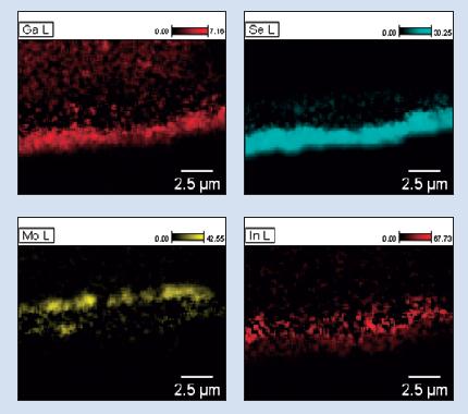
24 Delaminated CIGS solar cell 3 SEM of a Cu(In,Ga)Se 2 solar cell (cross-section) and its mode of operation 3 D. Abou-Ras et al. Elemental distribution profiles across Cu(In,Ga)Se 2 solar-cell absorbers acquired by various techniques. In: M. Luysberg, K. Tillmann, T. Weirich (Eds.), EMC 2008, Vol 1: Instrumentation and Methods, Proceedings of the 14th European Microscopy Congress 2008, Aachen, Germany, September 1-5, 2008 (Springer, 2008) p Energy/environmental application Solar cells based on Cu(In, Ga)Se 2 (CIGS) Thin-film stack on glass (or in this case steel) Mo and Zn oxide layer form electrical contacts p-type CIGS film (sunlight absorber) and n-type CdS film form p-n junction Excellent efficiency Low cost compared to thicker silicon-based solar cells Practical problem Delamination of device Controlling film composition and interfacial chemistry between layers (affects electrical properties) Solution EDS imaging of good & delaminated areas High resolution elemental information XPS imaging & sputter depth profiling Elemental and composition information as a function of depth Identify delamination layer 24
25 Delaminated CIGS solar cell EDS Point Analysis Delamination zone Some of the CIGS material had delaminated from the substrate. Measurements were taken from the three distinct areas of the sample: (1 & 2) the top layers of the sample (3) the metallic surface electrical contact material (4) the underlying metallic substrate. 25

26 Delaminated CIGS solar cell EDS Point Analysis 26
27 Delaminated CIGS solar cell EDS Point Analysis Locations 1 and 2 on the film are the same material consisting of a majority of In and Se with a small amount of Cu and a small amount of Ga. Only small amounts of Zn, O, Cd and S are measured due to the thin nature of these layers. Location 3 on the metallic contact layer is silver. Location 4 where the film is removed shows the base Mo substrate that the layers are grown on. 27
28 Delaminated CIGS solar cell XPS Point Analysis XPS point analysis at the same locations as the EDS analysis 28
29 Delaminated CIGS solar cell XPS Elemental analysis Se3d Counts / s Ag3d C1s Mo3d In3d 1 & 2 Zn2p3 O1s Sn3d5 4 Ga2p3 3 Red spectrum is average of points 1 & Binding Energy (ev) 29
30 Area 1 XPS Chemical analysis 3.40E+04 Sn3d Scan 1.80E+05 In3d Scan 3.20E E+05 Counts / s 3.00E E E E E+04 SnO Element Counts / s 1.40E E E E E E+04 Element InOx 2.00E E E E Binding Energy (ev) Binding Energy (ev) 6.00E+04 O1s Scan 7000 C1s Scan Counts / s 5.00E E E E+04 Metal CO3 Metal oxide Counts / s carbonate C-C or C-H carbide Cl2s (Metal ClO4) Chemical state analysis suggests that points 1 & 2 are indium-tin-oxide (ITO) 1.00E Binding Energy (ev) Binding Energy (ev) 30
 Counts / s 1.40E+05 1.20E+05 1.00E+05 8.00E+04 6.00E+04 4.00E+04 2.")
31 Area 3 XPS Chemical analysis 3000 S2p Scan 1.40E+04 C1s Scan 1.60E+05 Ag3d Scan Counts / s Metal SO4 organic SO2 Metal SO3 Element Metal S Counts / s 1.20E E E E E+03 carbonate C-C or C-H carbide Cl2s (Metal ClO4) Counts / s 1.40E E E E E E E+04 Element Ag2O AgO E E Binding Energy (ev) Binding Energy (ev) Binding Energy (ev) 2900 Cl2p Scan 1.50E+04 O1s Scan Counts / s Metal ClO4 Metal Cl Counts / s 1.40E E E+04 Metal CO3 Metal oxide E E Binding Energy (ev) Binding Energy (ev) 31
32 Delaminated CIGS solar cell Point analysis comparison EDS Ga-K Zn-K O-K Cr-K In-L Cd-L Ag-L Mo-L Se-K Fe-K Cu-K Area Area Area Area XPS Ga2p3 Zn2p3 O1s Sn3d5 In3d Ag3d Mo3d Se3d C1s S2p Cl2p Area 1/ Area Area EDS shows the presence of the expected stack components. XPS shows the presence of small contaminants, and the nature of the outer layer. 32

33 Delaminated CIGS solar cell XPS Mapping 33


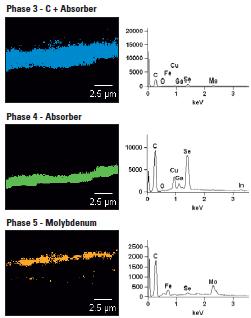
34 Delaminated CIGS solar cell XPS Phase Analysis Phase 1 Phase 2 Phase 3 Phase 4 Phase 5 Se3d S2p Mo3d C1s Ag3d Cd3d In3d Sn3d O1s A O1s B Zn2p Ga2p

35 CIGS solar cell Cross-section of CIGS film stack Low Magnification A Spectral Imaging mapping analysis was performed at low magnification on the cross-section sample to understand all of the layers that constitute the material. The thickness of all of the layers was approximately 1/3 mm. 35

36 CIGS solar cell Cross-section of CIGS film stack 36

37 CIGS solar cell Cross-section of CIGS film stack 37


38 Delaminated CIGS solar cell XPS Depth Profile 3keV Ar+ ion beam 60s etch time Compucentric rotation Depth scale calibrated to EDS result 38
39 Delaminated CIGS solar cell XPS Depth Profile ITO CIGS Mo Cr Steel Atomic percent (%) ZnO CdS Se3d S2p Mo3d C1s Cd3d5 In3d5 Sn3d5 O1s A O1s B Cr2p3 Fe2p3 Cu2p3 Zn2p3 Ga2p Etch Depth (nm) 39
40 Delaminated CIGS solar cell XPS Depth Profile 1.40E E+04 In3d E+04 Atomic percent (%) Counts / s 8.00E E E E E Binding Energy (ev) Se3d S2p Mo3d C1s Cd3d5 In3d5 Sn3d5 O1s A O1s B Cr2p3 Fe2p3 Cu2p3 Zn2p3 Ga2p Etch Depth (nm) 40
41 Delaminated CIGS solar cell XPS Depth Profile CIGS Mo Cr Steel Atomic percent (%) Se3d S2p Mo3d C1s In3d5 O1s A O1s B Cr2p3 Fe2p Etch Depth (nm) 41
42 Delaminated CIGS solar cell XPS Depth Profile ITO CIGS Mo Cr Steel ZnO CdS 42
43 Delaminated CIGS solar cell XPS Depth Profile CIGS Mo Cr Steel 43

44 Delaminated CIGS solar cell XPS Depth Profile Delamination zone Ga/In gradient Ag contact 44
45 Acknowledgements Oak Ridge National Laboratory (HTML) RJ Lee Group Application specialists in East Grinstead, UK & Madison, USA 45
ToF-SIMS or XPS? Xinqi Chen Keck-II
 ToF-SIMS or XPS? Xinqi Chen Keck-II 1 Time of Flight Secondary Ion Mass Spectrometry (ToF-SIMS) Not ToF MS (laser, solution) X-ray Photoelectron Spectroscopy (XPS) 2 3 Modes of SIMS 4 Secondary Ion Sputtering
Characterizing Materials for Energy Generation Using X-ray Photoelectron Spectroscopy (XPS)
") Characterizing Materials for Energy Generation Using X-ray Photoelectron Spectroscopy (XPS) Tim Nunney* and Richard White Thermo Fisher Scientific, The Birches, Imberhorne Lane, East Grinstead, West Sussex,
Characterizing Materials for Energy Generation Using X-ray Photoelectron Spectroscopy (XPS) Tim Nunney* and Richard White Thermo Fisher Scientific, The Birches, Imberhorne Lane, East Grinstead, West Sussex,
PHI 5000 Versaprobe-II Focus X-ray Photo-electron Spectroscopy
 PHI 5000 Versaprobe-II Focus X-ray Photo-electron Spectroscopy The very basic theory of XPS XPS theroy Surface Analysis Ultra High Vacuum (UHV) XPS Theory XPS = X-ray Photo-electron Spectroscopy X-ray
X-Ray Photoelectron Spectroscopy (XPS) Prof. Paul K. Chu
 Prof. Paul K. Chu") X-Ray Photoelectron Spectroscopy (XPS) Prof. Paul K. Chu X-ray Photoelectron Spectroscopy Introduction Qualitative analysis Quantitative analysis Charging compensation Small area analysis and XPS imaging
X-Ray Photoelectron Spectroscopy (XPS) Prof. Paul K. Chu X-ray Photoelectron Spectroscopy Introduction Qualitative analysis Quantitative analysis Charging compensation Small area analysis and XPS imaging
Introduction to X-ray Photoelectron Spectroscopy (XPS) XPS which makes use of the photoelectric effect, was developed in the mid-1960
 XPS which makes use of the photoelectric effect, was developed in the mid-1960") Introduction to X-ray Photoelectron Spectroscopy (XPS) X-ray Photoelectron Spectroscopy (XPS), also known as Electron Spectroscopy for Chemical Analysis (ESCA) is a widely used technique to investigate
Introduction to X-ray Photoelectron Spectroscopy (XPS) X-ray Photoelectron Spectroscopy (XPS), also known as Electron Spectroscopy for Chemical Analysis (ESCA) is a widely used technique to investigate
Electron probe microanalysis - Electron microprobe analysis EPMA (EMPA) What s EPMA all about? What can you learn?
 What s EPMA all about? What can you learn?") Electron probe microanalysis - Electron microprobe analysis EPMA (EMPA) What s EPMA all about? What can you learn? EPMA - what is it? Precise and accurate quantitative chemical analyses of micron-size
Electron probe microanalysis - Electron microprobe analysis EPMA (EMPA) What s EPMA all about? What can you learn? EPMA - what is it? Precise and accurate quantitative chemical analyses of micron-size
MT Electron microscopy Scanning electron microscopy and electron probe microanalysis
 MT-0.6026 Electron microscopy Scanning electron microscopy and electron probe microanalysis Eero Haimi Research Manager Outline 1. Introduction Basics of scanning electron microscopy (SEM) and electron
Applications of Micro-Area Analysis Used by JPS-9200 X-ray Photoelectron Spectrometer
 Applications of Micro-Area Analysis Used by JPS-9200 X-ray Photoelectron Spectrometer Yoshitoki Iijima Application & Research Center, JEOL Ltd. Introduction Recently, with advances in the development of
Auger Electron Spectroscopy
 Auger Electron Spectroscopy Auger Electron Spectroscopy is an analytical technique that provides compositional information on the top few monolayers of material. Detect all elements above He Detection
Auger Electron Spectroscopy Overview
 Auger Electron Spectroscopy Overview Also known as: AES, Auger, SAM 1 Auger Electron Spectroscopy E KLL = E K - E L - E L AES Spectra of Cu EdN(E)/dE Auger Electron E N(E) x 5 E KLL Cu MNN Cu LMM E f E
X- ray Photoelectron Spectroscopy and its application in phase- switching device study
 X- ray Photoelectron Spectroscopy and its application in phase- switching device study Xinyuan Wang A53073806 I. Background X- ray photoelectron spectroscopy is of great importance in modern chemical and
An Introduction to Auger Electron Spectroscopy
 An Introduction to Auger Electron Spectroscopy Spyros Diplas MENA3100 SINTEF Materials & Chemistry, Department of Materials Physics & Centre of Materials Science and Nanotechnology, Department of Chemistry,
Photoemission Spectroscopy
 FY13 Experimental Physics - Auger Electron Spectroscopy Photoemission Spectroscopy Supervisor: Per Morgen SDU, Institute of Physics Campusvej 55 DK - 5250 Odense S Ulrik Robenhagen,
EDS User School. Principles of Electron Beam Microanalysis
 EDS User School Principles of Electron Beam Microanalysis Outline 1.) Beam-specimen interactions 2.) EDS spectra: Origin of Bremsstrahlung and characteristic peaks 3.) Moseley s law 4.) Characteristic
X-ray photoelectron spectroscopy - An introduction
 X-ray photoelectron spectroscopy - An introduction Spyros Diplas spyros.diplas@sintef.no spyros.diplas@smn.uio.no SINTEF Materials & Chemistry, Materials Physics -Oslo & Centre of Materials Science and
QUESTIONS AND ANSWERS
 QUESTIONS AND ANSWERS (1) For a ground - state neutral atom with 13 protons, describe (a) Which element this is (b) The quantum numbers, n, and l of the inner two core electrons (c) The stationary state
Lecture 5. X-ray Photoemission Spectroscopy (XPS)
") Lecture 5 X-ray Photoemission Spectroscopy (XPS) 5. Photoemission Spectroscopy (XPS) 5. Principles 5.2 Interpretation 5.3 Instrumentation 5.4 XPS vs UV Photoelectron Spectroscopy (UPS) 5.5 Auger Electron
Lecture 5 X-ray Photoemission Spectroscopy (XPS) 5. Photoemission Spectroscopy (XPS) 5. Principles 5.2 Interpretation 5.3 Instrumentation 5.4 XPS vs UV Photoelectron Spectroscopy (UPS) 5.5 Auger Electron
Auger Electron Spectroscopy *
 OpenStax-CNX module: m43546 1 Auger Electron Spectroscopy * Amanda M. Goodman Andrew R. Barron This work is produced by OpenStax-CNX and licensed under the Creative Commons Attribution License 3.0 1 Basic
Auger Electron Spectroscopy (AES) Prof. Paul K. Chu
 Prof. Paul K. Chu") Auger Electron Spectroscopy (AES) Prof. Paul K. Chu Auger Electron Spectroscopy Introduction Principles Instrumentation Qualitative analysis Quantitative analysis Depth profiling Mapping Examples The Auger
Auger Electron Spectroscopy (AES) Prof. Paul K. Chu Auger Electron Spectroscopy Introduction Principles Instrumentation Qualitative analysis Quantitative analysis Depth profiling Mapping Examples The Auger
MT Electron microscopy Scanning electron microscopy and electron probe microanalysis
 MT-0.6026 Electron microscopy Scanning electron microscopy and electron probe microanalysis Eero Haimi Research Manager Outline 1. Introduction Basics of scanning electron microscopy (SEM) and electron
X-ray Photoelectron Spectroscopy/ Electron spectroscopy for chemical analysis (ESCA), By Francis Chindeka
, By Francis Chindeka") X-ray Photoelectron Spectroscopy/ Electron spectroscopy for chemical analysis (ESCA), By Francis Chindeka X-ray photoelectron spectroscopy (XPS) or Electron spectroscopy for chemical analysis (ESCA), Surface
X-ray Photoelectron Spectroscopy/ Electron spectroscopy for chemical analysis (ESCA), By Francis Chindeka X-ray photoelectron spectroscopy (XPS) or Electron spectroscopy for chemical analysis (ESCA), Surface
Gaetano L Episcopo. Scanning Electron Microscopy Focus Ion Beam and. Pulsed Plasma Deposition
 Gaetano L Episcopo Scanning Electron Microscopy Focus Ion Beam and Pulsed Plasma Deposition Hystorical background Scientific discoveries 1897: J. Thomson discovers the electron. 1924: L. de Broglie propose
Auger Electron Spectroscopy (AES)
") 1. Introduction Auger Electron Spectroscopy (AES) Silvia Natividad, Gabriel Gonzalez and Arena Holguin Auger Electron Spectroscopy (Auger spectroscopy or AES) was developed in the late 1960's, deriving
1. Introduction Auger Electron Spectroscopy (AES) Silvia Natividad, Gabriel Gonzalez and Arena Holguin Auger Electron Spectroscopy (Auger spectroscopy or AES) was developed in the late 1960's, deriving
Reduced preferential sputtering of TiO 2 (and Ta 2 O 5 ) thin films through argon cluster ion bombardment.
 thin films through argon cluster ion bombardment.") NATIOMEM Reduced preferential sputtering of TiO 2 (and Ta 2 O 5 ) thin films through argon cluster ion bombardment. R. Grilli *, P. Mack, M.A. Baker * * University of Surrey, UK ThermoFisher Scientific
NATIOMEM Reduced preferential sputtering of TiO 2 (and Ta 2 O 5 ) thin films through argon cluster ion bombardment. R. Grilli *, P. Mack, M.A. Baker * * University of Surrey, UK ThermoFisher Scientific
Spectroscopy on Mars!
 Spectroscopy on Mars! Pathfinder Spirit and Opportunity Real World Friday H2A The Mars Pathfinder: Geological Elemental Analysis On December 4th, 1996, the Mars Pathfinder was launched from earth to begin
Application of Surface Analysis for Root Cause Failure Analysis
 Application of Surface Analysis for Root Cause Failure Analysis David A. Cole Evans Analytical Group East Windsor, NJ Specialists in Materials Characterization Outline Introduction X-Ray Photoelectron
X-Ray Photoelectron Spectroscopy (XPS) Auger Electron Spectroscopy (AES)
 Auger Electron Spectroscopy (AES)") X-Ray Photoelectron Spectroscopy (XPS) Auger Electron Spectroscopy (AES) XPS X-ray photoelectron spectroscopy (XPS) is one of the most used techniques to chemically characterize the surface. Also known
X-Ray Photoelectron Spectroscopy (XPS) Auger Electron Spectroscopy (AES) XPS X-ray photoelectron spectroscopy (XPS) is one of the most used techniques to chemically characterize the surface. Also known
Thermo Scientific K-Alpha + XPS Spectrometer. Fast, powerful and accessible chemical analysis for surface and thin film characterization
 Thermo Scientific K-Alpha + XPS Spectrometer Fast, powerful and accessible chemical analysis for surface and thin film characterization X-ray Photoelectron Spectroscopy Quantitative, chemical identification
MS482 Materials Characterization ( 재료분석 ) Lecture Note 4: XRF
 Lecture Note 4: XRF") 2016 Fall Semester MS482 Materials Characterization ( 재료분석 ) Lecture Note 4: XRF Byungha Shin Dept. of MSE, KAIST 1 Course Information Syllabus 1. Overview of various characterization techniques (1 lecture)
2016 Fall Semester MS482 Materials Characterization ( 재료분석 ) Lecture Note 4: XRF Byungha Shin Dept. of MSE, KAIST 1 Course Information Syllabus 1. Overview of various characterization techniques (1 lecture)
Supporting Information s for
 Supporting Information s for # Self-assembling of DNA-templated Au Nanoparticles into Nanowires and their enhanced SERS and Catalytic Applications Subrata Kundu* and M. Jayachandran Electrochemical Materials
Interfacial Chemistry and Adhesion Phenomena: How to Analyse and How to Optimise
 Interfacial Chemistry and Adhesion Phenomena: How to Analyse and How to Optimise John F Watts Department of Mechanical Engineering Sciences The Role of Surface Analysis in Adhesion Studies Assessing surface
X-ray photoelectron spectroscopy - An introduction
 X-ray photoelectron spectroscopy - An introduction Spyros Diplas SINTEF Materials & Chemistry, Sector of Materials and Nanotechnology, Department of Materials Physics-Oslo & Centre of Materials Science
The design of an integrated XPS/Raman spectroscopy instrument for co-incident analysis
 The design of an integrated XPS/Raman spectroscopy instrument for co-incident analysis Tim Nunney The world leader in serving science 2 XPS Surface Analysis XPS +... UV Photoelectron Spectroscopy UPS He(I)
Advanced Lab Course. X-Ray Photoelectron Spectroscopy 1 INTRODUCTION 1 2 BASICS 1 3 EXPERIMENT Qualitative analysis Chemical Shifts 7
 Advanced Lab Course X-Ray Photoelectron Spectroscopy M210 As of: 2015-04-01 Aim: Chemical analysis of surfaces. Content 1 INTRODUCTION 1 2 BASICS 1 3 EXPERIMENT 3 3.1 Qualitative analysis 6 3.2 Chemical
Application of the GD-Profiler 2 to the PV domain
 Application of the GD-Profiler 2 to the PV domain GD Profiler 2 RF GDOES permits to follow the distribution of the elements as function of depth. This is an ultra fast characterisation technique capable
e - Galvanic Cell 1. Voltage Sources 1.1 Polymer Electrolyte Membrane (PEM) Fuel Cell
 Fuel Cell") Galvanic cells convert different forms of energy (chemical fuel, sunlight, mechanical pressure, etc.) into electrical energy and heat. In this lecture, we are interested in some examples of galvanic cells.
Galvanic cells convert different forms of energy (chemical fuel, sunlight, mechanical pressure, etc.) into electrical energy and heat. In this lecture, we are interested in some examples of galvanic cells.
Methods of surface analysis
 Methods of surface analysis Nanomaterials characterisation I RNDr. Věra Vodičková, PhD. Surface of solid matter: last monoatomic layer + absorbed monolayer physical properties are effected (crystal lattice
MICRO-TOMOGRAPHY AND X-RAY ANALYSIS OF GEOLOGICAL SAMPLES
 THE PUBLISHING HOUSE PROCEEDINGS OF THE ROMANIAN ACADEMY, Series A, OF THE ROMANIAN ACADEMY Volume 18, Number 1/2017, pp. 42 49 MICRO-TOMOGRAPHY AND X-RAY ANALYSIS OF GEOLOGICAL SAMPLES Ion GRUIA University
Overview of X-Ray Fluorescence Analysis
 Overview of X-Ray Fluorescence Analysis AMPTEK, INC., Bedford, MA 01730 Ph: +1 781 275 2242 Fax: +1 781 275 3470 sales@amptek.com 1 What is X-Ray Fluorescence (XRF)? A physical process: Emission of characteristic
Photoelectron spectroscopy Instrumentation. Nanomaterials characterization 2
 Photoelectron spectroscopy Instrumentation Nanomaterials characterization 2 RNDr. Věra V Vodičkov ková,, PhD. Photoelectron Spectroscopy general scheme Impact of X-ray emitted from source to the sample
The Use of Synchrotron Radiation in Modern Research
 The Use of Synchrotron Radiation in Modern Research Physics Chemistry Structural Biology Materials Science Geochemical and Environmental Science Atoms, molecules, liquids, solids. Electronic and geometric
Chemistry Instrumental Analysis Lecture 19 Chapter 12. Chem 4631
 Chemistry 4631 Instrumental Analysis Lecture 19 Chapter 12 There are three major techniques used for elemental analysis: Optical spectrometry Mass spectrometry X-ray spectrometry X-ray Techniques include:
Surface and Interface Characterization of Polymer Films
 Surface and Interface Characterization of Polymer Films Jeff Shallenberger, Evans Analytical Group 104 Windsor Center Dr., East Windsor NJ Copyright 2013 Evans Analytical Group Outline Introduction to
Birck Nanotechnology Center XPS: X-ray Photoelectron Spectroscopy ESCA: Electron Spectrometer for Chemical Analysis
 Birck Nanotechnology Center XPS: X-ray Photoelectron Spectroscopy ESCA: Electron Spectrometer for Chemical Analysis Dmitry Zemlyanov Birck Nanotechnology Center, Purdue University Outline Introduction
Multi-technique photoelectron spectrometer for micro-area spectroscopy and imaging
 Multi-technique photoelectron spectrometer for micro-area spectroscopy and imaging U. Manju, M. Sreemony and A. K. Chakraborty In this note we present the new multipurpose photoelectron spectroscopy facility
X-Ray Photoelectron Spectroscopy (XPS)
") X-Ray Photoelectron Spectroscopy (XPS) Louis Scudiero http://www.wsu.edu/~scudiero; 5-2669 Electron Spectroscopy for Chemical Analysis (ESCA) The basic principle of the photoelectric effect was enunciated
X-Ray Photoelectron Spectroscopy (XPS) Louis Scudiero http://www.wsu.edu/~scudiero; 5-2669 Electron Spectroscopy for Chemical Analysis (ESCA) The basic principle of the photoelectric effect was enunciated
Applications of XPS, AES, and TOF-SIMS
 Applications of XPS, AES, and TOF-SIMS Scott R. Bryan Physical Electronics 1 Materials Characterization Techniques Microscopy Optical Microscope SEM TEM STM SPM AFM Spectroscopy Energy Dispersive X-ray
Chemistry 311: Instrumentation Analysis Topic 2: Atomic Spectroscopy. Chemistry 311: Instrumentation Analysis Topic 2: Atomic Spectroscopy
 Topic 2b: X-ray Fluorescence Spectrometry Text: Chapter 12 Rouessac (1 week) 4.0 X-ray Fluorescence Download, read and understand EPA method 6010C ICP-OES Winter 2009 Page 1 Atomic X-ray Spectrometry Fundamental
MS482 Materials Characterization ( 재료분석 ) Lecture Note 12: Summary. Byungha Shin Dept. of MSE, KAIST
 Lecture Note 12: Summary. Byungha Shin Dept. of MSE, KAIST") 2015 Fall Semester MS482 Materials Characterization ( 재료분석 ) Lecture Note 12: Summary Byungha Shin Dept. of MSE, KAIST 1 Course Information Syllabus 1. Overview of various characterization techniques (1
2015 Fall Semester MS482 Materials Characterization ( 재료분석 ) Lecture Note 12: Summary Byungha Shin Dept. of MSE, KAIST 1 Course Information Syllabus 1. Overview of various characterization techniques (1
A DIVISION OF ULVAC-PHI
 A DIVISION OF ULVAC-PHI X-ray photoelectron spectroscopy (XPS/ESCA) is the most widely used surface analysis technique and has many well established industrial and research applications. XPS provides
HOW TO APPROACH SCANNING ELECTRON MICROSCOPY AND ENERGY DISPERSIVE SPECTROSCOPY ANALYSIS. SCSAM Short Course Amir Avishai
 HOW TO APPROACH SCANNING ELECTRON MICROSCOPY AND ENERGY DISPERSIVE SPECTROSCOPY ANALYSIS SCSAM Short Course Amir Avishai RESEARCH QUESTIONS Sea Shell Cast Iron EDS+SE Fe Cr C Objective Ability to ask the
for XPS surface analysis
 Thermo Scientific Avantage XPS Software Powerful instrument operation and data processing for XPS surface analysis Avantage Software Atomic Concentration (%) 100 The premier software for surface analysis
Spin-resolved photoelectron spectroscopy
 Spin-resolved photoelectron spectroscopy Application Notes Spin-resolved photoelectron spectroscopy experiments were performed in an experimental station consisting of an analysis and a preparation chamber.
Electron Spectroscopy
 Electron Spectroscopy Photoelectron spectroscopy is based upon a single photon in/electron out process. The energy of a photon is given by the Einstein relation : E = h ν where h - Planck constant ( 6.62
X-ray Absorption Spectroscopy
 X-ray Absorption Spectroscopy Nikki Truss November 26, 2012 Abstract In these experiments, some aspects of x-ray absorption spectroscopy were investigated. The x-ray spectrum of molybdenum was recorded
Characterization of Secondary Emission Materials for Micro-Channel Plates. S. Jokela, I. Veryovkin, A. Zinovev
 Characterization of Secondary Emission Materials for Micro-Channel Plates S. Jokela, I. Veryovkin, A. Zinovev Secondary Electron Yield Testing Technique We have incorporated XPS, UPS, Ar-ion sputtering,
ECE Semiconductor Device and Material Characterization
 ECE 4813 Semiconductor Device and Material Characterization Dr. Alan Doolittle School of Electrical and Computer Engineering Georgia Institute of Technology As with all of these lecture slides, I am indebted
Modern Optical Spectroscopy
 Modern Optical Spectroscopy X-Ray Microanalysis Shu-Ping Lin, Ph.D. Institute of Biomedical Engineering E-mail: splin@dragon.nchu.edu.tw Website: http://web.nchu.edu.tw/pweb/users/splin/ Backscattered
X Rays & Crystals. Characterizing Mineral Chemistry & Structure. J.D. Price
 X Rays & Crystals Characterizing Mineral Chemistry & Structure J.D. Price Light - electromagnetic spectrum Wave behavior vs. particle behavior If atoms are on the 10-10 m scale, we need to use sufficiently
X-Ray Photoelectron Spectroscopy (XPS)
") X-Ray Photoelectron Spectroscopy (XPS) Louis Scudiero http://www.wsu.edu/~scudiero; 5-2669 Fulmer 261A Electron Spectroscopy for Chemical Analysis (ESCA) The basic principle of the photoelectric effect
X-Ray Photoelectron Spectroscopy (XPS) Louis Scudiero http://www.wsu.edu/~scudiero; 5-2669 Fulmer 261A Electron Spectroscopy for Chemical Analysis (ESCA) The basic principle of the photoelectric effect
An Introduction to Diffraction and Scattering. School of Chemistry The University of Sydney
 An Introduction to Diffraction and Scattering Brendan J. Kennedy School of Chemistry The University of Sydney 1) Strong forces 2) Weak forces Types of Forces 3) Electromagnetic forces 4) Gravity Types
Fast, Effective XPS Point Analysis of Metal Components
 Application Note: 52297 Fast, Effective XPS Point Analysis of Metal Components Chris Baily and Tim Nunney, Thermo Fisher Scientific, East Grinstead, West Sussex, UK Key Words K-Alpha Auto-Analysis Multi-Spectrum
MS482 Materials Characterization ( 재료분석 ) Lecture Note 2: UPS
 Lecture Note 2: UPS") 2016 Fall Semester MS482 Materials Characterization ( 재료분석 ) Lecture Note 2: UPS Byungha Shin Dept. of MSE, KAIST 1 Course Information Syllabus 1. Overview of various characterization techniques (1 lecture)
2016 Fall Semester MS482 Materials Characterization ( 재료분석 ) Lecture Note 2: UPS Byungha Shin Dept. of MSE, KAIST 1 Course Information Syllabus 1. Overview of various characterization techniques (1 lecture)
Generation of X-Rays in the SEM specimen
 Generation of X-Rays in the SEM specimen The electron beam generates X-ray photons in the beam-specimen interaction volume beneath the specimen surface. Some X-ray photons emerging from the specimen have
Energy Spectroscopy. Excitation by means of a probe
 Energy Spectroscopy Excitation by means of a probe Energy spectral analysis of the in coming particles -> XAS or Energy spectral analysis of the out coming particles Different probes are possible: Auger
X-ray Spectroscopy. Danny Bennett and Maeve Madigan. October 12, 2015
 X-ray Spectroscopy Danny Bennett and Maeve Madigan October 12, 2015 Abstract Various X-ray spectra were obtained, and their properties were investigated. The characteristic peaks were identified for a
Fabrication of a One-dimensional Tube-in-tube Polypyrrole/Tin oxide Structure for Highly Sensitive DMMP Sensor Applications
 Electronic Supplementary Material (ESI) for Journal of Materials Chemistry A. This journal is The Royal Society of Chemistry 2017 Electronic Supplementary Information (ESI) for Fabrication of a One-dimensional
Supporting Information
 Electronic Supplementary Material (ESI) for Nanoscale. This journal is The Royal Society of Chemistry 2014 Engineering Cu 2 O/NiO/Cu 2 MoS 4 Hybrid Photocathode for H 2 Generation in Water Chen Yang, a,b
Chemical Analysis in TEM: XEDS, EELS and EFTEM. HRTEM PhD course Lecture 5
 Chemical Analysis in TEM: XEDS, EELS and EFTEM HRTEM PhD course Lecture 5 1 Part IV Subject Chapter Prio x-ray spectrometry 32 1 Spectra and mapping 33 2 Qualitative XEDS 34 1 Quantitative XEDS 35.1-35.4
X-Ray Photoelectron Spectroscopy (XPS)-2
-2") X-Ray Photoelectron Spectroscopy (XPS)-2 Louis Scudiero http://www.wsu.edu/~scudiero; 5-2669 Fulmer 261A Electron Spectroscopy for Chemical Analysis (ESCA) The 3 step model: 1.Optical excitation 2.Transport
X-Ray Photoelectron Spectroscopy (XPS)-2 Louis Scudiero http://www.wsu.edu/~scudiero; 5-2669 Fulmer 261A Electron Spectroscopy for Chemical Analysis (ESCA) The 3 step model: 1.Optical excitation 2.Transport
Practical Surface Analysis
 Practical Surface Analysis SECOND EDITION Volume 1 Auger and X-ray Photoelectron Spectroscopy Edited by D. BRIGGS ICI PLC, Wilton Materials Research Centre, Wilton, Middlesbrough, Cleveland, UK and M.
PHI. Scanning XPS Microprobe
 PHI Scanning XPS Microprobe Unique Scanning XPS Microprobe X-ray photoelectron spectroscopy (XPS/ESA) is the most widely used surface analysis technique and has many well established industrial and research
Nanostructured Ti 0.7 Mo 0.3 O 2 Support Enhances Electron Transfer to Pt : High-Performance Catalyst for Oxygen Reduction Reaction
 Nanostructured Ti 0.7 Mo 0.3 O 2 Support Enhances Electron Transfer to Pt : High-Performance Catalyst for Oxygen Reduction Reaction Seonbaek Ha Professor : Carlo U. Segre 12. 06. 2013 Department of Chemical
5) Surface photoelectron spectroscopy. For MChem, Spring, Dr. Qiao Chen (room 3R506) University of Sussex.
 Surface photoelectron spectroscopy. For MChem, Spring, Dr. Qiao Chen (room 3R506) University of Sussex.") For MChem, Spring, 2009 5) Surface photoelectron spectroscopy Dr. Qiao Chen (room 3R506) http://www.sussex.ac.uk/users/qc25/ University of Sussex Today s topics 1. Element analysis with XPS Binding energy,
For MChem, Spring, 2009 5) Surface photoelectron spectroscopy Dr. Qiao Chen (room 3R506) http://www.sussex.ac.uk/users/qc25/ University of Sussex Today s topics 1. Element analysis with XPS Binding energy,
Energy Spectroscopy. Ex.: Fe/MgO
 Energy Spectroscopy Spectroscopy gives access to the electronic properties (and thus chemistry, magnetism,..) of the investigated system with thickness dependence Ex.: Fe/MgO Fe O Mg Control of the oxidation
raw materials C V Mn Mg S Al Ca Ti Cr Si G H Nb Na Zn Ni K Co A B C D E F
 Today s advanced batteries require a range of specialized analytical tools to better understand the electrochemical processes that occur during battery cycling. Evans Analytical Group (EAG) offers a wide-range
Chapter 9. Electron mean free path Microscopy principles of SEM, TEM, LEEM
 Chapter 9 Electron mean free path Microscopy principles of SEM, TEM, LEEM 9.1 Electron Mean Free Path 9. Scanning Electron Microscopy (SEM) -SEM design; Secondary electron imaging; Backscattered electron
Atomic Physics. Chapter 6 X ray. Jinniu Hu 24/12/ /20/13
 Atomic Physics Chapter 6 X ray 11/20/13 24/12/2018 Jinniu Hu 1!1 6.1 The discovery of X ray X-rays were discovered in 1895 by the German physicist Wilhelm Roentgen. He found that a beam of high-speed electrons
CHARACTERIZATION of NANOMATERIALS KHP
 CHARACTERIZATION of NANOMATERIALS Overview of the most common nanocharacterization techniques MAIN CHARACTERIZATION TECHNIQUES: 1.Transmission Electron Microscope (TEM) 2. Scanning Electron Microscope
Supporting Information
 Supporting Information Pt Nanoparticles Anchored Molecular Self-Assemblies of DNA: An Extremely Stable and Efficient HER Electrocatalyst with Ultra-Low Pt Content Sengeni Anantharaj, $ Pitchiah E. Karthik,
MS482 Materials Characterization ( 재료분석 ) Lecture Note 5: RBS
 Lecture Note 5: RBS") 2016 Fall Semester MS482 Materials Characterization ( 재료분석 ) Lecture Note 5: RBS Byungha Shin Dept. of MSE, KAIST 1 Course Information Syllabus 1. Overview of various characterization techniques (1 lecture)
2016 Fall Semester MS482 Materials Characterization ( 재료분석 ) Lecture Note 5: RBS Byungha Shin Dept. of MSE, KAIST 1 Course Information Syllabus 1. Overview of various characterization techniques (1 lecture)
Fig. S1 The Structure of RuCE(Left) and RuCA (Right)
 and RuCA (Right)") Supporting information Fabrication of CZTS and CZTSSe photocathode CZTS photocathode was fabricated by sulfurization of a stacked film containing Cu, Zn and Sn. The stacked film was fabricated on Mo coated
Supporting information Fabrication of CZTS and CZTSSe photocathode CZTS photocathode was fabricated by sulfurization of a stacked film containing Cu, Zn and Sn. The stacked film was fabricated on Mo coated
XPS & Scanning Auger Principles & Examples
 XPS & Scanning Auger Principles & Examples Shared Research Facilities Lunch Talk Contact info: dhu Pujari & Han Zuilhof Lab of rganic Chemistry Wageningen University E-mail: dharam.pujari@wur.nl Han.Zuilhof@wur.nl
Supplementary Information for. Silver Nanoparticles Embedded Anti-microbial Paints Based on Vegetable Oil
 Supplementary Information for Silver Nanoparticles Embedded Anti-microbial Paints Based on Vegetable Oil Ashavani Kumar #, Praveen Kumar Vemula #, Pulickel M. Ajayan, George John * Department of Chemistry,
XPS Depth Profiling of Epitaxial Graphene Intercalated with FeCl 3
 XPS Depth Profiling of Epitaxial Graphene Intercalated with FeCl 3 Mahdi Ibrahim Maynard H. Jackson High School Atlanta, GA. Faculty Advisor: Dr. Kristin Shepperd Research Group: Prof. Edward Conrad School
Theta Probe: A tool for characterizing ultra thin films and self assembled monolayers using parallel angle resolved XPS (ARXPS)
") Theta Probe: A tool for characterizing ultra thin films and self assembled monolayers using parallel angle resolved XPS (ARXPS) C. E. Riley, P. Mack, T. S. Nunney and R. G. White Thermo Fisher Scientific
Theta Probe: A tool for characterizing ultra thin films and self assembled monolayers using parallel angle resolved XPS (ARXPS) C. E. Riley, P. Mack, T. S. Nunney and R. G. White Thermo Fisher Scientific
XPS Surface Characterization of Disposable Laboratory Gloves and the Transfer of Glove Components to Other Surfaces
 Application Note: 52287 XPS Surface Characterization of Disposable Laboratory Gloves and the Transfer of Glove Components to Other Surfaces Brian R. Strohmeier, Thermo Fisher Scientific, Madison, WI, USA
IV. Surface analysis for chemical state, chemical composition
 IV. Surface analysis for chemical state, chemical composition Probe beam Detect XPS Photon (X-ray) Photoelectron(core level electron) UPS Photon (UV) Photoelectron(valence level electron) AES electron
Bonds in molecules are formed by the interactions between electrons.
 CHEM 2060 Lecture 6: Electrostatic Interactions L6-1 PART TWO: Electrostatic Interactions In the first section of this course, we were more concerned with structural aspects of molecules. In this section
ABC s of Electrochemistry series Materials Characterization techniques: SEM and EDS Ana María Valenzuela-Muñiz November 3, 2011
 ABC s of Electrochemistry series Materials Characterization techniques: SEM and EDS Ana María Valenzuela-Muñiz November 3, 2011 CEER, Department of Chemical and Biomolecular Engineering Outline Introduction
Cross Section of Proton Exchange Membrane Fuel Cell
 PEMFC Electrodes 1 Cross Section of Proton Exchange Membrane Fuel Cell Anode Cathode 2 Typical PEMFC Electrodes: - Anode Hydrogen Oxidation - Pt Ru / C - Cathode Oxygen reduction - Pt / C Pt is alloyed
A DIVISION OF ULVAC-PHI. Quantera II. Scanning XPS Microprobe
 A DIVISION OF ULVAC-PHI Quantera II Scanning XPS Microprobe X-ray Photoelectron Spectroscopy (XPS/ESCA) is the most widely used surface analysis technique and has many well established industrial and
X-ray photoelectron spectroscopic characterization of molybdenum nitride thin films
 Korean J. Chem. Eng., 28(4), 1133-1138 (2011) DOI: 10.1007/s11814-011-0036-2 INVITED REVIEW PAPER X-ray photoelectron spectroscopic characterization of molybdenum nitride thin films Jeong-Gil Choi Department
Transparent Electrode Applications
 Transparent Electrode Applications LCD Solar Cells Touch Screen Indium Tin Oxide (ITO) Zinc Oxide (ZnO) - High conductivity - High transparency - Resistant to environmental effects - Rare material (Indium)
X-RAY SPECTRA. Theory:
 12 Oct 18 X-ray.1 X-RAY SPECTRA In this experiment, a number of measurements involving x-rays will be made. The spectrum of x-rays emitted from a molybdenum target will be measured, and the experimental
Surface Chemistry and Reaction Dynamics of Electron Beam Induced Deposition Processes
 Surface Chemistry and Reaction Dynamics of Electron Beam Induced Deposition Processes e -? 2 nd FEBIP Workshop Thun, Switzerland 2008 Howard Fairbrother Johns Hopkins University Baltimore, MD, USA Outline
Secondary Ion Mass Spectroscopy (SIMS)
") Secondary Ion Mass Spectroscopy (SIMS) Analyzing Inorganic Solids * = under special conditions ** = semiconductors only + = limited number of elements or groups Analyzing Organic Solids * = under special
Secondary Ion Mass Spectroscopy (SIMS) Analyzing Inorganic Solids * = under special conditions ** = semiconductors only + = limited number of elements or groups Analyzing Organic Solids * = under special
Chapter Six: X-Rays. 6.1 Discovery of X-rays
 Chapter Six: X-Rays 6.1 Discovery of X-rays In late 1895, a German physicist, W. C. Roentgen was working with a cathode ray tube in his laboratory. He was working with tubes similar to our fluorescent
Electronics Supplementary Information for. Manab Kundu, Cheuk Chi Albert Ng, Dmitri Y. Petrovykh and Lifeng Liu*
 Electronics Supplementary Information for Nickel foam supported mesoporous MnO 2 nanosheet arrays with superior lithium storage performance Manab Kundu, Cheuk Chi Albert Ng, Dmitri Y. Petrovykh and Lifeng
Photoelectron Spectroscopy. Xiaozhe Zhang 10/03/2014
 Photoelectron Spectroscopy Xiaozhe Zhang 10/03/2014 A conception last time remain Secondary electrons are electrons generated as ionization products. They are called 'secondary' because they are generated